WO2009133781A1 - フィールド機器 - Google Patents
フィールド機器 Download PDFInfo
- Publication number
- WO2009133781A1 WO2009133781A1 PCT/JP2009/057845 JP2009057845W WO2009133781A1 WO 2009133781 A1 WO2009133781 A1 WO 2009133781A1 JP 2009057845 W JP2009057845 W JP 2009057845W WO 2009133781 A1 WO2009133781 A1 WO 2009133781A1
- Authority
- WO
- WIPO (PCT)
- Prior art keywords
- current
- power supply
- unit
- field device
- control element
- Prior art date
- Legal status (The legal status is an assumption and is not a legal conclusion. Google has not performed a legal analysis and makes no representation as to the accuracy of the status listed.)
- Ceased
Links
Images

Classifications
-
- G—PHYSICS
- G05—CONTROLLING; REGULATING
- G05B—CONTROL OR REGULATING SYSTEMS IN GENERAL; FUNCTIONAL ELEMENTS OF SUCH SYSTEMS; MONITORING OR TESTING ARRANGEMENTS FOR SUCH SYSTEMS OR ELEMENTS
- G05B9/00—Safety arrangements
- G05B9/02—Safety arrangements electric
-
- G—PHYSICS
- G01—MEASURING; TESTING
- G01R—MEASURING ELECTRIC VARIABLES; MEASURING MAGNETIC VARIABLES
- G01R19/00—Arrangements for measuring currents or voltages or for indicating presence or sign thereof
-
- G—PHYSICS
- G08—SIGNALLING
- G08C—TRANSMISSION SYSTEMS FOR MEASURED VALUES, CONTROL OR SIMILAR SIGNALS
- G08C19/00—Electric signal transmission systems
- G08C19/02—Electric signal transmission systems in which the signal transmitted is magnitude of current or voltage
Definitions
- This invention relates to a field device that adjusts the value of a current flowing through a two-wire transmission line according to a measured value.
- the original measurement and control functions are usually performed continuously, while the secondary functions operate at a fixed or non-fixed period in response to a command from the CPU, and the other functions are not operated. ing. That is, the secondary function is operated only when necessary by a command from the CPU.
- Fig. 4 shows the configuration of the main part of a conventional 2-wire field device.
- reference numeral 100A denotes a field device
- reference numeral 200A denotes a host device (monitoring device) connected to the field device 100A via a two-wire transmission line AL (AL1, AL2).
- AL two-wire transmission line
- the field device 100A is a differential pressure / pressure transmitter.
- the field device 100A includes a sensor unit 1A that generates an analog signal corresponding to the magnitude of the pressure or differential pressure, an A / D converter 2A that converts the analog signal from the sensor unit 1A into a digital signal, A CPU 3A that samples a digital signal output from the A / D converter 2A to obtain a measured value of pressure / differential pressure, and a digital current value obtained by the CPU 3A within a predetermined current range (4 to 20 mA).
- the communication unit 5A for outputting the analog signal output from the D / A converter 4A to the two-wire transmission line AL, and the two-wire transmission line AL
- a voltage regulator (first power supply unit) 6A that generates a stable DC voltage V1 (DC 6.5V) as a first power source based on the obtained current of 4 to 20 mA, and this voltage level Provided between the voltage regulator 7A, the alarm drive circuit 8A, and the voltage regulator 7A and the alarm drive circuit 8A, which generates a stable DC voltage V2 (DC3V) as a second power supply upon receiving the power supply from the regulator 6A.
- the changeover switch 9A, the ROM 10A, and the RAM 11A are provided.
- the CPU 3A operates in response to the supply of power from the voltage regulator 7A, and operates according to the program stored in the ROM 10A while accessing the RAM 11A.
- the ROM 10A in addition to the measurement value processing program that samples the digital signal from the A / D converter 2A, obtains the measurement value of the pressure / differential pressure, and notifies the monitoring device 200A of the measurement value, an abnormality occurring in the own device is detected.
- a changeover switch control program for turning on the changeover switch 9A is stored.
- the measurement value calculation unit 3A1 and the changeover switch control unit 3A2 are shown as functional blocks in the CPU 3A. However, the measurement value calculation unit 3A1 and the changeover switch control unit 3A2 are processing functions according to a program in the CPU 3A. Realized.
- the alarm driving circuit 8 is a contact output circuit using a photocoupler having a light emitting part and a light receiving part.
- the changeover switch 9A when the changeover switch 9A is turned on, the current from the voltage regulator 7A flows as a drive current to the light emitting portion of the alarm drive circuit (photocoupler) 8A, and the light from the light emitting portion that emits light in response to this drive current. Is received by the light receiving unit, the contact output on the light receiving unit side is turned on, and the alarm circuit 300A provided outside is activated.
- the reason why the alarm driving circuit 8A is a photocoupler is to ensure electrical insulation of input and output so that noise that affects the processing operation of the CPU 3A does not occur.
- the alarm drive circuit 8A requires a current of 1 mA or more as a drive current to the light emitting portion of the photocoupler. Therefore, when a high performance CPU is used as the CPU 3A, the CPU 3A is driven. The power to do is insufficient.
- the present invention has been made to solve such a problem, and its purpose is to provide a secondary function that operates only when necessary without degrading the performance of the original processing function. It is to provide a field device that can work.
- the present invention provides a current value adjusting means for adjusting a value of a current flowing through a two-wire transmission line according to a measured value, and a first power source from the current flowing through the transmission line.
- a load circuit provided in a current shunting path to the control circuit, and if necessary, control the element state of the current control element in the processing unit and supply a current to the second power supply unit flowing through the supply path.
- Current control element control means is provided for diverting the shunt passage by an amount necessary for the operation of the load circuit.
- the processing unit controls the element state of the current control element as necessary, and distributes the current to the second power supply unit flowing through the supply passage by an amount necessary for the operation of the load circuit. To divert. That is, when it is not necessary to activate a secondary function, the current flowing through the supply passage is sent to the second power supply unit without being divided into the branch passage.
- the processing unit controls the element state of the current control element and diverts the current flowing through the supply passage to the shunt passage. At this time, the current to be diverted to the diversion passage is set to an amount necessary for operation of the load circuit. The current shunted in the shunt passage is sent to the second power supply unit through the load circuit.
- the merging current of the current from the supply passage and the current from the shunt passage is supplied to the second power supply unit.
- the amount of current supplied to the second power supply unit is the same as that in the case where it is not necessary to activate the secondary function, there is no shortage of power supplied to the processing unit.
- a secondary function that operates only when necessary can be activated without degrading the performance of the original processing function.
- a current control element is provided in a current supply path from the first power supply section to the second power supply section, and a current shunt path from the first power supply section to the second power supply section is provided. Is provided with a load circuit, the element state of the current control element is controlled in the processing unit as necessary, and the current to the second power supply unit flowing through the supply passage is distributed in an amount necessary for the operation of the load circuit.
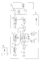
- FIG. 1 is a block diagram showing a main part of an embodiment of a field device according to the present invention.
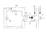
- FIG. 2 is a diagram showing a main part of a circuit example when an FET is used as a current control element in this field device.
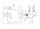
- FIG. 3 is a diagram showing a main part of a circuit example in the case where an alarm driving circuit is used as the pulse output circuit of the counter circuit in this field device.
- FIG. 4 is a block diagram showing a configuration of a main part of a conventional two-wire field device.
- FIG. 1 is a block diagram showing a main part of an embodiment of a field device according to the present invention.
- 100 is a field device according to the present invention
- 200 is a host device (monitoring device) connected to the field device 100 via a two-wire transmission line L (L1, L2).
- L two-wire transmission line
- the field device 100 is a differential pressure / pressure transmitter.
- the field device 100 includes a sensor unit 1 that generates an analog signal corresponding to the magnitude of pressure or differential pressure, an A / D converter 2 that converts the analog signal from the sensor unit 1 into a digital signal, A CPU 3 that samples a digital signal output from the A / D converter 2 to obtain a measured value of pressure / differential pressure, and a digital current value obtained by the CPU 3 within a predetermined current range (4 to 20 mA).
- a D / A converter 4 for converting to an analog signal
- a communication unit 5 for outputting an analog signal output from the D / A converter 4 to a two-wire transmission line L, and a two-wire transmission line L
- a voltage regulator (first power supply unit) 6 that generates a stable DC voltage V1 (DC6.5V) as a first power source based on the obtained current of 4 to 20 mA, and supply of power from the voltage regulator 6
- a voltage regulator 7 to generate stable DC voltage V2 to (DC3V) as the second power receiving, alarm driving circuit 8, and a ROM 10, a RAM 11, a current control element 12.
- the field device 100 is greatly different from the conventional field device 100A in that a current control element 12 is provided in a current supply path LA from the voltage regulator 6 to the voltage regulator 7, and a voltage regulator 7 from the voltage regulator 6 is provided.
- a current control element 12 is provided in a current supply path LA from the voltage regulator 6 to the voltage regulator 7, and a voltage regulator 7 from the voltage regulator 6 is provided.
- an alarm drive circuit 8 is provided in the current diversion path LB, and that the element state of the current control element 12 is controlled by the CPU 3 as necessary.
- the current control element 12 for example, a MOS-FET, J-type FET, bipolar transistor, variable resistance element or the like is used.
- a case where a variable resistance element is used as the current control element 12 is shown for easy understanding.
- the CPU 3 controls the resistance value of the current control element 12 as the element state of the current control element 12.
- the CPU 3 operates in response to the supply of power from the voltage regulator 7, and operates according to the program stored in the ROM 10 while accessing the RAM 11.
- the ROM 10 has its own program as a program specific to this embodiment.
- a current control element control program for detecting an abnormality occurring in the device and controlling the resistance value of the current control element 12 is stored.
- the measurement value calculation unit 3-1 and the current control element control unit 3-3 are shown as functional blocks in the CPU 3, but the measurement value calculation unit 3-1 and the current control element control unit 3- 3 is realized as a processing function according to a program in the CPU 3.
- the alarm driving circuit 8 is a contact output circuit using a photocoupler having a light emitting part and a light receiving part.
- the current control element control unit 3-3 sets the resistance value of the current control element 12 to zero. Thereby, the current IA flowing through the supply passage LA is sent to the voltage regulator 7 without being divided into the branch passage LB.
- IB 0.
- the current control element control unit 3-3 controls the resistance value of the current control element 12, and sets the supply path LB.
- the flowing current is divided into the diversion passage LB.
- the current IB to be diverted to the diversion passage LB is set to an amount necessary for the operation of the alarm driving circuit 8.
- the alarm drive circuit 8 requires a current of 1 mA or more as a drive current to the light emitting part of the photocoupler.
- the current control element control unit 3-3 restricts the current IA flowing through the supply path LA by adjusting the resistance value of the current control element 12, and a part of the current IA that has been flowing through the supply path LA until then is shunted.
- the drive current required for the operation of the alarm drive circuit 8 is secured as the shunt current IB.
- the shunt current IB flows as a drive current to the light emitting part of the alarm drive circuit (photocoupler) 8, and the light from the light emitting part that emits light in response to this drive current is received by the light receiving part, and contact output on the light receiving part side Is turned on, and the alarm circuit 300 provided outside operates.
- the shunt current IB supplied to the alarm driving circuit 8 is sent to the voltage regulator 7 through the light emitting unit of the alarm driving circuit 8.
- the voltage regulator 7 is supplied with a combined current of the current IA from the supply passage LA and the current IB from the shunt passage LB.
- the amount of current supplied to the voltage regulator 7 is the same as when the alarm drive circuit 8 does not need to be operated, so that the power supplied to the CPU 3 is not insufficient.
- the alarm driving circuit 8 can be operated without degrading the performance of the CPU 3 (without degrading the performance of the original processing function).
- the CPU 3 controls the resistance value of the current control element 12 as necessary, and diverts the current IA to the voltage regulator 7 flowing through the supply passage LA into the shunt passage LB.
- the control of the resistance value of the current control element 12 is permitted when it is determined that the current operation IA to the voltage regulator 7 flowing through the supply passage LA is not affected even if the current IA is divided into the branch passage LB. You may do it.
- a current control element control permission unit 3-2 for permitting control of the resistance value of the current control element 12 is provided.
- the alarm drive circuit 8 is operated by diverting the current IA to the voltage regulator 7 flowing through the supply path LA to the diversion path LB, the power supply fluctuations occur and the processing operation in the CPU 3 is affected.
- the control of the resistance value of the current control element 12 is prohibited by detecting this in advance. As a result, the alarm driving circuit 8 can be operated without affecting the original processing function of the CPU 3.
- FIG. 2 shows a main part of a circuit example when an FET is used as the current control element 12.
- D1 is a light emitting diode provided as a light emitting part of the alarm driving circuit 8
- FT1 is a phototransistor provided as a light receiving part of the alarm driving circuit 8
- the phototransistor FT1 is a power supply 301 of the alarm circuit 300 and an alarm. It is inserted and connected in a series circuit connecting a load 302 such as a lamp.
- the alarm driving circuit 8 is a photocoupler, but it goes without saying that the alarm drive circuit 8 is not limited to a photocoupler.
- the alarm drive circuit 8 includes an input unit that operates upon receiving the supply of the current IB from the shunt path LB, and an output unit that is turned on by the operation of the input unit.
- the input unit and the output unit are electrically connected.
- the alarm driving circuit 8 is used as the contact output circuit of the alarm circuit 300.
- the alarm driving circuit 8 is used as the pulse output circuit of the counter circuit 400 including the counter 401. You may make it use. Further, an alarm lamp may be provided in place of the alarm drive circuit 8, or an alarm buzzer may be provided.
- the processing unit that performs a predetermined operation upon receiving power supply from the voltage regulator 7 is the CPU 3.
- the processing unit is not necessarily a CPU, and may be a hardware circuit having a similar processing function. Good.
- the field device of the present invention can be used in various fields such as process control as a field device that adjusts the value of a current flowing through a two-wire transmission line according to a measured value.
Landscapes
- Physics & Mathematics (AREA)
- General Physics & Mathematics (AREA)
- Engineering & Computer Science (AREA)
- Automation & Control Theory (AREA)
- Arrangements For Transmission Of Measured Signals (AREA)
- Control Of Voltage And Current In General (AREA)
- Emergency Alarm Devices (AREA)
Abstract
Description
副次的な機能を働かせる必要がない場合、すなわちアラーム駆動回路8を作動させる必要がない場合、電流制御素子制御部3-3は、電流制御素子12の抵抗値を0とする。これにより、供給通路LAを流れている電流IAは、分流通路LBに分流されずに、電圧レギュレータ7に送られる。ここで、分流通路LBを流れる電流をIBとすると、IB=0とされる。
副次的な機能を働かせる必要がある場合、すなわちアラーム駆動回路8を作動させる必要がある場合、電流制御素子制御部3-3は、電流制御素子12の抵抗値を制御し、供給通路LBを流れている電流を分流通路LBに分流させる。この際、分流通路LBへ分流する電流IBは、アラーム駆動回路8の動作に必要な量とする。
Claims (4)
- 2線式の伝送路を流れる電流の値を計測値に応じて調整する電流値調整手段と、
前記伝送路を流れる電流から第1の電源を生成する第1の電源部と、
この第1の電源部からの電源の供給を受けて第2の電源を生成する第2の電源部と、
この第2の電源部からの電源の供給を受けて所定の処理動作を行う処理部と、
前記第1の電源部からの前記第2の電源部への電流の供給通路に設けられた電流制御素子と、
前記第1の電源部からの前記第2の電源部への電流の分流通路に設けられた負荷回路とを備え、
前記処理部は、
必要に応じて前記電流制御素子の素子状態を制御し、前記供給通路を流れている前記第2の電源部への電流を前記負荷回路の動作に必要な量だけ前記分流通路に分流させる電流制御素子制御手段
を備えることを特徴とするフィールド機器。 - 請求項1に記載されたフィールド機器において、
前記処理部は、
前記所定の処理動作として前記伝送路に流れる電流の値を計測値に応じて調整する処理動作を含む処理を行う中央演算処理装置である
ことを特徴とするフィールド機器。 - 請求項1に記載されたフィールド機器において、
前記処理部は、
前記供給通路を流れている前記第2の電源部への電流を前記分流通路に分流させても自己の処理動作に影響がないと判断した場合に前記電流制御素子の素子状態の制御を許可する手段
を備えることを特徴とするフィールド機器。 - 請求項1に記載されたフィールド機器において、
前記負荷回路は、
前記分流通路からの電流の供給を受けて動作する入力部と、この入力部の動作によってオンとされる出力部とを備え、前記入力部と前記出力部とが電気的に絶縁された絶縁型スイッチである
ことを特徴とするフィールド機器。
Priority Applications (4)
| Application Number | Priority Date | Filing Date | Title |
|---|---|---|---|
| US12/989,686 US8872486B2 (en) | 2008-04-28 | 2009-04-20 | Field instrument having a current control element |
| KR1020107019619A KR101085331B1 (ko) | 2008-04-28 | 2009-04-20 | 필드 기기 |
| CN2009801148323A CN102016741B (zh) | 2008-04-28 | 2009-04-20 | 现场仪表 |
| EP09738718.7A EP2284637B1 (en) | 2008-04-28 | 2009-04-20 | Field instrument |
Applications Claiming Priority (2)
| Application Number | Priority Date | Filing Date | Title |
|---|---|---|---|
| JP2008116859A JP5222015B2 (ja) | 2008-04-28 | 2008-04-28 | フィールド機器 |
| JP2008-116859 | 2008-04-28 |
Publications (1)
| Publication Number | Publication Date |
|---|---|
| WO2009133781A1 true WO2009133781A1 (ja) | 2009-11-05 |
Family
ID=41254998
Family Applications (1)
| Application Number | Title | Priority Date | Filing Date |
|---|---|---|---|
| PCT/JP2009/057845 Ceased WO2009133781A1 (ja) | 2008-04-28 | 2009-04-20 | フィールド機器 |
Country Status (6)
| Country | Link |
|---|---|
| US (1) | US8872486B2 (ja) |
| EP (1) | EP2284637B1 (ja) |
| JP (1) | JP5222015B2 (ja) |
| KR (1) | KR101085331B1 (ja) |
| CN (1) | CN102016741B (ja) |
| WO (1) | WO2009133781A1 (ja) |
Families Citing this family (85)
| Publication number | Priority date | Publication date | Assignee | Title |
|---|---|---|---|---|
| JP5865669B2 (ja) * | 2011-10-21 | 2016-02-17 | アズビル株式会社 | 光電スイッチ |
| US9679712B2 (en) * | 2012-10-16 | 2017-06-13 | Delta Systems, Inc. | Switch assembly and method of using same |
| DE102013103454A1 (de) * | 2013-04-08 | 2014-10-09 | Endress + Hauser Gmbh + Co. Kg | Messumformerspeisegerät, System zum Einsatz in der Automatisierungstechnik, sowie Verfahren zum Bedienen eines solchen Systems |
| US11397492B2 (en) | 2015-06-22 | 2022-07-26 | Sigmasense, Llc. | Enhanced mutual capacitance touch screen display with shape detection and methods for use therewith |
| US10664098B2 (en) | 2015-06-22 | 2020-05-26 | Sigmasense, Llc. | Channel driver circuit |
| US11907484B2 (en) | 2015-06-22 | 2024-02-20 | Sigmasense, Llc. | Function and orientation identification for input/output (I/O) operative touch sensor device (TSD) |
| KR101948453B1 (ko) | 2015-07-06 | 2019-02-14 | 시그마센스, 엘엘씨. | 내부 압력 기울기 회전을 갖는 펜 시스템 |
| US12194344B2 (en) | 2016-08-18 | 2025-01-14 | Sigmasense, Llc. | Plurality of layers of pressure sensors within a foot force detection system |
| US12207703B2 (en) | 2016-08-18 | 2025-01-28 | Sigmasense, Llc. | Shoe to shoe communication within a foot force detection system |
| US12226674B2 (en) | 2016-08-18 | 2025-02-18 | Sigmasense, Llc. | Power harvesting in a foot force detection system |
| US12225979B2 (en) | 2016-08-18 | 2025-02-18 | Sigmasense, Llc. | Variable sampling rate within a foot force detection system |
| US12181352B2 (en) | 2021-06-03 | 2024-12-31 | Sigmasense, Llc. | Insole XYZ force detection system |
| US12446798B2 (en) | 2016-08-18 | 2025-10-21 | Sigmasense, Llc. | Personal monitoring system for monitoring body conditions using e-field communications |
| US12121773B2 (en) | 2016-08-18 | 2024-10-22 | Sigmasense, Llc. | Personal athlete monitoring system |
| US10838530B2 (en) | 2017-09-15 | 2020-11-17 | Sigmasense, Llc. | Touchscreen display with concurrent touch and display operations |
| US11822358B2 (en) | 2018-08-27 | 2023-11-21 | Sigmasense, Llc. | Drive-sense circuit to determine effects of different electrical characteristics on load |
| US12007421B2 (en) | 2018-08-27 | 2024-06-11 | Sigmasense, Llc. | Load sensing circuit employing sink and sense configuration |
| US11550426B2 (en) | 2018-08-27 | 2023-01-10 | Sigmasense, Llc. | Sensor monitoring system |
| US11635396B2 (en) | 2018-08-27 | 2023-04-25 | Sigmasense, Llc. | Sensing device with drive sense circuit and particle sensor and methods for use therewith |
| US11429226B2 (en) | 2018-08-27 | 2022-08-30 | Sigmasense, Llc. | Analog-digital drive sense circuit |
| US11003205B2 (en) | 2019-02-04 | 2021-05-11 | Sigmasense, Llc. | Receive analog to digital circuit of a low voltage drive circuit data communication system |
| US11644860B2 (en) | 2018-08-27 | 2023-05-09 | Sigmasense, Llc. | Configuring a programmable drive sense unit |
| US10554215B1 (en) | 2019-03-26 | 2020-02-04 | Sigmasense, Llc. | Analog to digital conversion circuit with very narrow bandpass digital filtering |
| US11914812B2 (en) | 2018-08-27 | 2024-02-27 | Sigmasense, Llc. | Current reference operative drive-sense circuit (DSC) |
| US11099032B2 (en) * | 2018-08-27 | 2021-08-24 | Sigmasense, Llc. | Drive sense circuit with drive-sense line |
| US10895867B2 (en) | 2018-08-27 | 2021-01-19 | Sigmasense, Llc. | Analog world interfacing for automated systems |
| US10908718B2 (en) | 2018-09-14 | 2021-02-02 | Sigmasense, Llc. | Large touch screen display with integrated electrodes |
| US11899867B2 (en) | 2018-09-14 | 2024-02-13 | Sigmasense, Llc. | Touch screen display with touchless gestures and methods for use therewith |
| US10845985B2 (en) | 2018-09-14 | 2020-11-24 | Sigmasense, Llc. | Identification in touch systems |
| US11875005B2 (en) | 2018-09-14 | 2024-01-16 | Sigmasense, Llc. | Touch screen display with touchless indications and methods for use therewith |
| US11372510B2 (en) | 2018-11-02 | 2022-06-28 | Sigmasense, Llc. | Multi-conductor touch system |
| US10852857B2 (en) | 2018-11-19 | 2020-12-01 | Sigmasense, Llc. | Frequency diverse e-pen for touch sensor and e-pen systems |
| US10935585B2 (en) | 2018-11-19 | 2021-03-02 | Sigmasense, Llc. | Drive sense circuit with transient suppression |
| US10996728B2 (en) | 2019-01-04 | 2021-05-04 | Sigmasense, Llc. | Power supply signal conditioning system based on drive-sense circuit (DSC) processing |
| US10915483B2 (en) | 2019-01-14 | 2021-02-09 | Sigmasense, Llc. | Low voltage drive circuit with variable oscillating characteristics and methods for use therewith |
| US10831690B2 (en) | 2019-01-14 | 2020-11-10 | Sigmasense, Llc. | Channel allocation among low voltage drive circuits |
| US10671034B1 (en) | 2019-03-18 | 2020-06-02 | Sigmasense, Llc. | Motor drive input adaptation with in-line drive-sense circuit |
| US11061082B2 (en) | 2019-03-18 | 2021-07-13 | Sigmasense, Llc. | Single line hall effect sensor drive and sense |
| US12046214B2 (en) | 2019-03-22 | 2024-07-23 | Sigmasense, Llc. | Display controller with row enable based on drive settle detection |
| US11029782B2 (en) | 2019-05-03 | 2021-06-08 | Sigmasense, Llc. | Light emitting diode (LED) touch display circuit |
| US11056930B2 (en) | 2019-05-31 | 2021-07-06 | Sigmasense, Llc. | Wireless power transfer and communications |
| US10756578B1 (en) | 2019-05-31 | 2020-08-25 | Sigmasense, Llc. | Wireless power transfer with in-line sensing and control |
| US11131714B2 (en) | 2019-05-31 | 2021-09-28 | Sigmasense, Llc. | Battery monitoring and characterization during charging |
| US11126297B2 (en) | 2019-06-10 | 2021-09-21 | Sigmasense, Llc. | Electronic pen with ring-back and other functionalities |
| US11216133B2 (en) | 2019-06-10 | 2022-01-04 | Sigmasense, Llc. | Device for use with a touch screen |
| US11555687B2 (en) | 2019-08-08 | 2023-01-17 | Sigmasense, Llc. | Capacitive imaging glove |
| US10976837B2 (en) | 2019-08-20 | 2021-04-13 | Sigmasense, Llc. | User input passive device for use with an interactive display device |
| US10908641B1 (en) | 2019-10-09 | 2021-02-02 | Sigmasense, Llc. | Display generated data transmission from user device to touchscreen via user |
| US11221980B2 (en) | 2019-10-31 | 2022-01-11 | Sigmasense, Llc. | Low voltage drive circuit operable to convey data via a bus |
| US11190205B2 (en) | 2019-11-08 | 2021-11-30 | Sigmasense, Llc. | Single-ended direct interface dual DAC feedback photo-diode sensor |
| US11133811B2 (en) | 2019-11-08 | 2021-09-28 | Sigmasense, Llc. | High resolution analog to digital converter (ADC) with improved bandwidth |
| US11709189B2 (en) | 2019-11-08 | 2023-07-25 | Sigmasense, Llc. | Two-element high accuracy impedance sensing circuit with increased signal to noise ratio (SNR) |
| US10862492B1 (en) | 2019-11-08 | 2020-12-08 | Sigmasense, Llc. | Current operative analog to digital converter (ADC) |
| US12352713B2 (en) | 2019-12-30 | 2025-07-08 | Sigmasense, Llc. | Organic and/or inorganic material test system using differential drive-sense circuits |
| US11935397B2 (en) | 2019-12-30 | 2024-03-19 | Sigmasense, Llc. | Organic and inorganic test system |
| US11216109B2 (en) | 2020-01-07 | 2022-01-04 | Sigmasense, Llc. | Drive-sense control for extended sensor panels |
| US11221704B2 (en) | 2020-02-05 | 2022-01-11 | Sigmasense, Llc. | Screen-to-screen communication via touch sense elements |
| US11079888B1 (en) | 2020-02-18 | 2021-08-03 | Sigmasense, Llc. | Sensitivity region of interest processing (ROIP) for input/output (I/O) operative touch sensor device (TSD) |
| US11144160B1 (en) | 2020-03-30 | 2021-10-12 | Sigmasense, Llc. | Three-dimensional data reduction method and system |
| US11182038B2 (en) | 2020-04-08 | 2021-11-23 | Sigmasense, Llc. | Encoded data pattern touchscreen sensing system |
| US11340995B2 (en) | 2020-05-21 | 2022-05-24 | Sigmasense, Llc. | Integrated circuit with programmable input/output module |
| US11504535B2 (en) | 2020-06-03 | 2022-11-22 | Sigmasense, Llc. | Pacemaker operative to deliver impulses of pace signal and sense cardiac response via single conductor of pacemaker lead |
| US11439812B2 (en) | 2020-06-03 | 2022-09-13 | Sigmasense, Llc. | Array operative to perform distributed/patterned sensing and/or stimulation across patient bodily section |
| US11304002B2 (en) | 2020-08-12 | 2022-04-12 | Sigmasense, Llc. | Single transducer audio in/out device |
| US11374587B1 (en) | 2021-02-25 | 2022-06-28 | Sigmasense, Llc. | Batteryless wireless sensor system |
| US20220342513A1 (en) | 2021-04-23 | 2022-10-27 | Sigmasense, Llc. | Processing z-direction pressure indication of a passive pen |
| US11575850B2 (en) | 2021-05-28 | 2023-02-07 | Sigmasense, Llc. | Imaging device with drive-sense circuit(s) and methods for use therewith |
| US11575851B2 (en) | 2021-05-28 | 2023-02-07 | Sigmasense, Llc. | Handheld communication device with drive-sense circuit based imaging array and methods for use therewith |
| US12085618B2 (en) | 2021-06-01 | 2024-09-10 | Sigmasense, Llc. | Battery serving network with multiple loads with individual voltage sensing at each load |
| US12360641B2 (en) | 2021-06-28 | 2025-07-15 | Sigmasense, Llc. | System for detecting and validating multiuser interaction with interface elements via perimeter sensors |
| US12373070B2 (en) | 2021-06-28 | 2025-07-29 | Sigmasense, Llc. | System for detecting and validating multiuser interaction with interface elements via signaling through users bodies |
| US11679678B2 (en) | 2021-06-28 | 2023-06-20 | Sigmasense, Llc. | Vehicle system for detecting and visually conveying vehicle button interaction |
| US11733818B2 (en) | 2021-07-19 | 2023-08-22 | Sigmasense, Llc. | Identifying capacitively coupled devices |
| US11556298B1 (en) | 2021-07-30 | 2023-01-17 | Sigmasense, Llc | Generation and communication of user notation data via an interactive display device |
| US11592874B1 (en) | 2021-08-04 | 2023-02-28 | Sigmasense, Llc. | Touch sensing in a flexible/foldable touch screen display |
| US11797139B2 (en) | 2021-09-21 | 2023-10-24 | Sigmasense, Llc. | Fingerprint scanning device incorporating drive-sense circuitry |
| US11435864B1 (en) | 2021-09-28 | 2022-09-06 | Sigmasense, Llc. | Differential touch screen display |
| US11709563B2 (en) | 2021-10-26 | 2023-07-25 | Sigmasense, Llc. | Touch-based device with interlaced electrode grids |
| US12271550B2 (en) | 2022-04-28 | 2025-04-08 | Sigmasense, Llc. | Multi-frequency character transmission and detection |
| US12360630B2 (en) | 2022-06-03 | 2025-07-15 | Sigmasense, Llc. | Touch sensor device with differentiated priority sensing region |
| US12175039B2 (en) | 2022-07-13 | 2024-12-24 | Sigmasense, Llc. | Touch icon offset based on touch data samples |
| US11740752B1 (en) | 2022-07-13 | 2023-08-29 | Sigmasense, Llc. | Device with signal generator |
| US12050740B2 (en) | 2022-11-29 | 2024-07-30 | Sigmasense, Llc. | Passive device with compressible pressure assembly for Z-direction capacitance detection |
| US12135852B1 (en) | 2023-04-28 | 2024-11-05 | Sigmasense, Llc. | Spatial filtering a touch signal of a touch screen display |
| US12541267B2 (en) | 2023-04-28 | 2026-02-03 | Sigmasense, Llc. | Touch sensor noise prediction and cancellation |
Citations (3)
| Publication number | Priority date | Publication date | Assignee | Title |
|---|---|---|---|---|
| JPH11183575A (ja) | 1997-12-17 | 1999-07-09 | Fuji Electric Co Ltd | フィールド機器の電池寿命予測方法 |
| JP2004151941A (ja) * | 2002-10-30 | 2004-05-27 | Yamatake Corp | フィールド機器 |
| JP2006323661A (ja) * | 2005-05-19 | 2006-11-30 | Yamatake Corp | 2線式フィールド機器および異常通知制御方法 |
Family Cites Families (12)
| Publication number | Priority date | Publication date | Assignee | Title |
|---|---|---|---|---|
| JP2707465B2 (ja) * | 1989-06-29 | 1998-01-28 | スタンレー電気株式会社 | インバータ装置 |
| JP3299556B2 (ja) | 1991-09-19 | 2002-07-08 | 株式会社日立製作所 | フィールド計器用コミュニケータ |
| US6822764B1 (en) * | 1996-04-23 | 2004-11-23 | Ricoh Company, Ltd. | Communication terminal with an energy saving capability |
| CA2347890C (en) * | 1998-11-03 | 2008-02-19 | Ametek, Inc. | High efficiency power supply for a two-wire loop powered device |
| US6684340B1 (en) * | 1999-10-07 | 2004-01-27 | Endress + Hauser Gmbh + Co. | Measuring instrument having two pairs of lines connected to two indentical pairs of terminals, via which signal current flows through one pair and supply current flows through the other pair |
| US6535161B1 (en) * | 2000-11-28 | 2003-03-18 | Mcewan Technologies, Llc | Loop powered radar rangefinder |
| US6930956B2 (en) * | 2002-01-18 | 2005-08-16 | Siemens Milltronics Process Instruments, Inc. | Current loop control circuit for a time of flight ranging system |
| EP1668324B1 (en) | 2003-09-30 | 2012-06-27 | Micro Motion, Inc. | Two-wire bus instrument |
| KR100619899B1 (ko) * | 2004-08-31 | 2006-09-12 | 엘지전자 주식회사 | 휴대단말기의 전력증폭기 전원 고속 스위칭 장치 및 방법 |
| DE102004063735A1 (de) | 2004-12-29 | 2006-07-20 | Endress + Hauser Flowtec Ag | Von einer externen elektrischen Energieversorgung gespeiste Feldgerät-Elektronik |
| US8000841B2 (en) * | 2005-12-30 | 2011-08-16 | Rosemount Inc. | Power management in a process transmitter |
| JP4869797B2 (ja) * | 2006-06-08 | 2012-02-08 | 三菱電機株式会社 | 接近検知システム |
-
2008
- 2008-04-28 JP JP2008116859A patent/JP5222015B2/ja active Active
-
2009
- 2009-04-20 CN CN2009801148323A patent/CN102016741B/zh active Active
- 2009-04-20 EP EP09738718.7A patent/EP2284637B1/en active Active
- 2009-04-20 KR KR1020107019619A patent/KR101085331B1/ko active Active
- 2009-04-20 WO PCT/JP2009/057845 patent/WO2009133781A1/ja not_active Ceased
- 2009-04-20 US US12/989,686 patent/US8872486B2/en not_active Expired - Fee Related
Patent Citations (3)
| Publication number | Priority date | Publication date | Assignee | Title |
|---|---|---|---|---|
| JPH11183575A (ja) | 1997-12-17 | 1999-07-09 | Fuji Electric Co Ltd | フィールド機器の電池寿命予測方法 |
| JP2004151941A (ja) * | 2002-10-30 | 2004-05-27 | Yamatake Corp | フィールド機器 |
| JP2006323661A (ja) * | 2005-05-19 | 2006-11-30 | Yamatake Corp | 2線式フィールド機器および異常通知制御方法 |
Non-Patent Citations (1)
| Title |
|---|
| See also references of EP2284637A4 |
Also Published As
| Publication number | Publication date |
|---|---|
| JP5222015B2 (ja) | 2013-06-26 |
| EP2284637A4 (en) | 2017-06-28 |
| CN102016741B (zh) | 2013-08-14 |
| EP2284637A1 (en) | 2011-02-16 |
| US20110043183A1 (en) | 2011-02-24 |
| KR101085331B1 (ko) | 2011-11-23 |
| US8872486B2 (en) | 2014-10-28 |
| KR20100111741A (ko) | 2010-10-15 |
| JP2009266066A (ja) | 2009-11-12 |
| EP2284637B1 (en) | 2019-09-04 |
| CN102016741A (zh) | 2011-04-13 |
Similar Documents
| Publication | Publication Date | Title |
|---|---|---|
| JP5222015B2 (ja) | フィールド機器 | |
| GB2462776A (en) | Power converters with rate of change monitoring for fault prediction and/or detection | |
| JP2002297246A5 (ja) | ||
| US20090140749A1 (en) | Device for Measuring a Load Current | |
| WO2009142100A1 (ja) | ハイサイドドライバ | |
| JP6476835B2 (ja) | 信号変換装置 | |
| JP5656713B2 (ja) | フィールド機器 | |
| CN101351687A (zh) | 具有电能管理功能的过程变送器及其电能管理方法 | |
| US10484052B2 (en) | Method and device for transmitting electrical power and/or signals between a wall and a leaf pivotable relative thereto | |
| US4794372A (en) | Two-wire DC signal telemetering system | |
| CN102568388B (zh) | 双线过程装置的动态功率控制 | |
| CA2458869C (en) | Two wire output/power mechanism for remote devices | |
| CA2933993A1 (en) | Device for measuring voltage across a remote load | |
| US20160154045A1 (en) | Sensor circuit, vehicle and method therefor | |
| KR20110066163A (ko) | 센서 시스템용 제어 장치, 센서 시스템 및 센서 시스템에서의 신호 전달 방법 | |
| US7982597B2 (en) | Device for detecting current-impressed signals in security systems | |
| JP2007124136A5 (ja) | ||
| EP2733564B1 (en) | Two-wire transmitter starter circuit and two-wire transmitter including the same | |
| AU2010291310B2 (en) | Excitation device for an electric machine comprising a superconducting load | |
| JP2010123025A (ja) | フィールド機器 | |
| CN102187180B (zh) | 过程自动化现场设备 | |
| JP2012053819A (ja) | 2線式伝送器 | |
| JP2011049925A (ja) | 電源タップ、端末装置及び通信システム | |
| ATE342530T1 (de) | Diagnosefähiges netzgerät | |
| CN112636786A (zh) | 现场设备耦合装置和现场设备 |
Legal Events
| Date | Code | Title | Description |
|---|---|---|---|
| WWE | Wipo information: entry into national phase |
Ref document number: 200980114832.3 Country of ref document: CN |
|
| 121 | Ep: the epo has been informed by wipo that ep was designated in this application |
Ref document number: 09738718 Country of ref document: EP Kind code of ref document: A1 |
|
| ENP | Entry into the national phase |
Ref document number: 20107019619 Country of ref document: KR Kind code of ref document: A |
|
| WWE | Wipo information: entry into national phase |
Ref document number: 12989686 Country of ref document: US |
|
| NENP | Non-entry into the national phase |
Ref country code: DE |
|
| WWE | Wipo information: entry into national phase |
Ref document number: 2009738718 Country of ref document: EP |