WO2009136586A1 - 有機電界発光素子用化合物及び有機電界発光素子 - Google Patents
有機電界発光素子用化合物及び有機電界発光素子 Download PDFInfo
- Publication number
- WO2009136586A1 WO2009136586A1 PCT/JP2009/058451 JP2009058451W WO2009136586A1 WO 2009136586 A1 WO2009136586 A1 WO 2009136586A1 JP 2009058451 W JP2009058451 W JP 2009058451W WO 2009136586 A1 WO2009136586 A1 WO 2009136586A1
- Authority
- WO
- WIPO (PCT)
- Prior art keywords
- group
- compound
- organic
- layer
- ring
- Prior art date
- Legal status (The legal status is an assumption and is not a legal conclusion. Google has not performed a legal analysis and makes no representation as to the accuracy of the status listed.)
- Ceased
Links
- GTJPJGVPTUXBBI-UHFFFAOYSA-N CC1=[O]COC(C)=C1 Chemical compound CC1=[O]COC(C)=C1 GTJPJGVPTUXBBI-UHFFFAOYSA-N 0.000 description 1
Images

Classifications
-
- H—ELECTRICITY
- H10—SEMICONDUCTOR DEVICES; ELECTRIC SOLID-STATE DEVICES NOT OTHERWISE PROVIDED FOR
- H10K—ORGANIC ELECTRIC SOLID-STATE DEVICES
- H10K50/00—Organic light-emitting devices
-
- C—CHEMISTRY; METALLURGY
- C07—ORGANIC CHEMISTRY
- C07F—ACYCLIC, CARBOCYCLIC OR HETEROCYCLIC COMPOUNDS CONTAINING ELEMENTS OTHER THAN CARBON, HYDROGEN, HALOGEN, OXYGEN, NITROGEN, SULFUR, SELENIUM OR TELLURIUM
- C07F9/00—Compounds containing elements of Groups 5 or 15 of the Periodic Table
- C07F9/02—Phosphorus compounds
- C07F9/547—Heterocyclic compounds, e.g. containing phosphorus as a ring hetero atom
- C07F9/553—Heterocyclic compounds, e.g. containing phosphorus as a ring hetero atom having one nitrogen atom as the only ring hetero atom
- C07F9/572—Five-membered rings
- C07F9/5728—Five-membered rings condensed with carbocyclic rings or carbocyclic ring systems
-
- C—CHEMISTRY; METALLURGY
- C07—ORGANIC CHEMISTRY
- C07F—ACYCLIC, CARBOCYCLIC OR HETEROCYCLIC COMPOUNDS CONTAINING ELEMENTS OTHER THAN CARBON, HYDROGEN, HALOGEN, OXYGEN, NITROGEN, SULFUR, SELENIUM OR TELLURIUM
- C07F9/00—Compounds containing elements of Groups 5 or 15 of the Periodic Table
- C07F9/02—Phosphorus compounds
- C07F9/547—Heterocyclic compounds, e.g. containing phosphorus as a ring hetero atom
- C07F9/6558—Heterocyclic compounds, e.g. containing phosphorus as a ring hetero atom containing at least two different or differently substituted hetero rings neither condensed among themselves nor condensed with a common carbocyclic ring or ring system
- C07F9/65583—Heterocyclic compounds, e.g. containing phosphorus as a ring hetero atom containing at least two different or differently substituted hetero rings neither condensed among themselves nor condensed with a common carbocyclic ring or ring system each of the hetero rings containing nitrogen as ring hetero atom
-
- C—CHEMISTRY; METALLURGY
- C09—DYES; PAINTS; POLISHES; NATURAL RESINS; ADHESIVES; COMPOSITIONS NOT OTHERWISE PROVIDED FOR; APPLICATIONS OF MATERIALS NOT OTHERWISE PROVIDED FOR
- C09K—MATERIALS FOR MISCELLANEOUS APPLICATIONS, NOT PROVIDED FOR ELSEWHERE
- C09K11/00—Luminescent materials, e.g. electroluminescent or chemiluminescent
- C09K11/06—Luminescent materials, e.g. electroluminescent or chemiluminescent containing organic luminescent materials
-
- H—ELECTRICITY
- H05—ELECTRIC TECHNIQUES NOT OTHERWISE PROVIDED FOR
- H05B—ELECTRIC HEATING; ELECTRIC LIGHT SOURCES NOT OTHERWISE PROVIDED FOR; CIRCUIT ARRANGEMENTS FOR ELECTRIC LIGHT SOURCES, IN GENERAL
- H05B33/00—Electroluminescent light sources
- H05B33/12—Light sources with substantially two-dimensional [2D] radiating surfaces
- H05B33/14—Light sources with substantially two-dimensional [2D] radiating surfaces characterised by the chemical or physical composition or the arrangement of the electroluminescent material, or by the simultaneous addition of the electroluminescent material in or onto the light source
-
- H—ELECTRICITY
- H10—SEMICONDUCTOR DEVICES; ELECTRIC SOLID-STATE DEVICES NOT OTHERWISE PROVIDED FOR
- H10K—ORGANIC ELECTRIC SOLID-STATE DEVICES
- H10K85/00—Organic materials used in the body or electrodes of devices covered by this subclass
- H10K85/60—Organic compounds having low molecular weight
- H10K85/649—Aromatic compounds comprising a hetero atom
- H10K85/657—Polycyclic condensed heteroaromatic hydrocarbons
- H10K85/6572—Polycyclic condensed heteroaromatic hydrocarbons comprising only nitrogen in the heteroaromatic polycondensed ring system, e.g. phenanthroline or carbazole
-
- C—CHEMISTRY; METALLURGY
- C09—DYES; PAINTS; POLISHES; NATURAL RESINS; ADHESIVES; COMPOSITIONS NOT OTHERWISE PROVIDED FOR; APPLICATIONS OF MATERIALS NOT OTHERWISE PROVIDED FOR
- C09K—MATERIALS FOR MISCELLANEOUS APPLICATIONS, NOT PROVIDED FOR ELSEWHERE
- C09K2211/00—Chemical nature of organic luminescent or tenebrescent compounds
- C09K2211/10—Non-macromolecular compounds
- C09K2211/1018—Heterocyclic compounds
- C09K2211/1025—Heterocyclic compounds characterised by ligands
- C09K2211/1044—Heterocyclic compounds characterised by ligands containing two nitrogen atoms as heteroatoms
-
- H—ELECTRICITY
- H10—SEMICONDUCTOR DEVICES; ELECTRIC SOLID-STATE DEVICES NOT OTHERWISE PROVIDED FOR
- H10K—ORGANIC ELECTRIC SOLID-STATE DEVICES
- H10K2101/00—Properties of the organic materials covered by group H10K85/00
- H10K2101/10—Triplet emission
-
- H—ELECTRICITY
- H10—SEMICONDUCTOR DEVICES; ELECTRIC SOLID-STATE DEVICES NOT OTHERWISE PROVIDED FOR
- H10K—ORGANIC ELECTRIC SOLID-STATE DEVICES
- H10K50/00—Organic light-emitting devices
- H10K50/10—OLEDs or polymer light-emitting diodes [PLED]
- H10K50/11—OLEDs or polymer light-emitting diodes [PLED] characterised by the electroluminescent [EL] layers
Definitions
- the present invention relates to a novel compound for organic electroluminescence device and an organic electroluminescence device using the same (hereinafter referred to as organic EL device).
- an organic electroluminescent element has a light emitting layer and a pair of counter electrodes sandwiching the layer as the simplest structure. That is, in an organic EL element, when an electric field is applied between both electrodes, electrons are injected from the cathode, holes are injected from the anode, and these are recombined in the light emitting layer to emit light. .
- CBP 4,4′-bis (9-carbazolyl) biphenyl
- CBP tris (2-phenylpyridine) iridium complex
- Ir (ppy) 3 which is a green phosphorescent light emitting material
- CBP is inferior to the hole transport ability
- the balance of charges in the light emitting layer is lost, and excess holes flow out to the cathode side, resulting in a decrease in luminous efficiency due to a decrease in recombination probability in the light emitting layer.
- the recombination region of the light emitting layer is limited to a narrow region near the interface on the cathode side, the electron transport with a low energy level of the lowest excited triplet state with respect to Ir (ppy) 3 such as Alq3 is low.
- the luminous efficiency may be lowered due to the transfer of triplet excitation energy from the dopant to the electron transport material.
- TAZ 3-phenyl-4- (1'-naphthyl) -5-phenyl-1,2,4-triazole
- NPB 4,4'-bis (N- (1-naphthyl) -N-phenylamino) biphenyl
- Patent Documents 4, 5 and 6 disclose the use of a certain kind of indolocarbazole compound for the organic EL element, and Patent Documents 7 and 8 use a certain kind of phosphoroxide compound for the organic EL element.
- Patent Documents 4, 5 and 6 disclose the use of a certain kind of indolocarbazole compound for the organic EL element
- Patent Documents 7 and 8 use a certain kind of phosphoroxide compound for the organic EL element.
- Patent Documents 4, 5 and 6 disclose the use of a certain kind of indolocarbazole compound for the organic EL element
- Patent Documents 7 and 8 use a certain kind of phosphoroxide compound for the organic EL element.
- a compound for an organic EL device having better performance.
- An object of this invention is to provide the practically useful organic EL element which has high efficiency and high drive stability in view of the said present condition, and a compound suitable for it.
- the present invention relates to an organic EL device using a specific indolocarbazole skeleton compound.
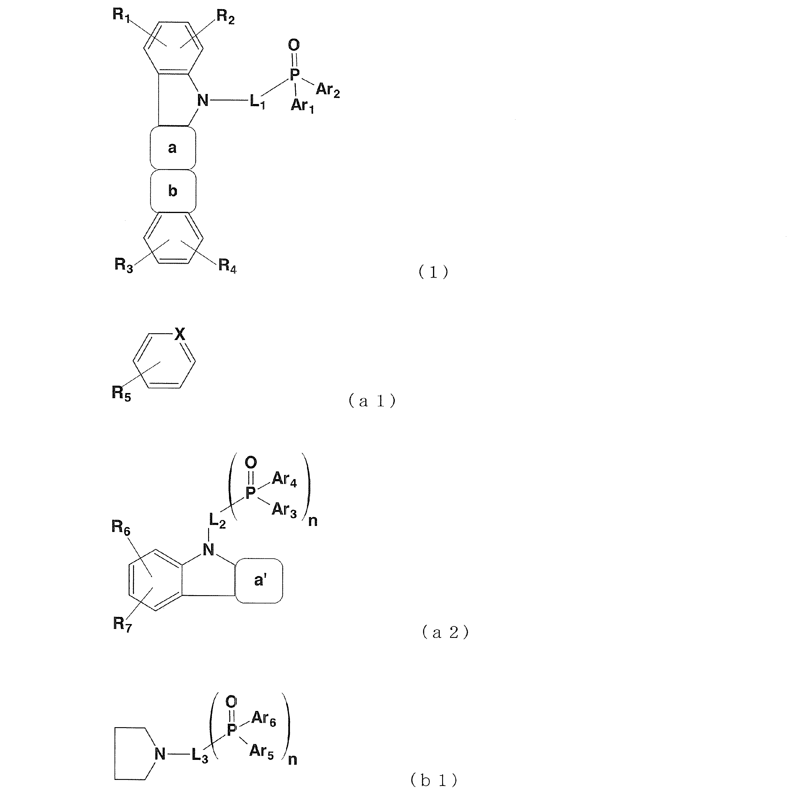
- the compound for organic electroluminescent elements of the present invention is represented by the following general formula (1).
- the ring a represents an aromatic ring or a heterocyclic ring represented by the formula (a1) or (a2) fused with two adjacent rings
- the ring a ′ is a formula (a1) fused with three adjacent rings.
- An aromatic ring or a heterocyclic ring represented by Ring b represents a heterocycle represented by the formula (b1) fused with two adjacent rings.
- X independently represents CR or N.
- Ar 1 to Ar 6 independently represent a substituted or unsubstituted aromatic hydrocarbon group or aromatic heterocyclic group.
- R and R 1 to R 7 are independently hydrogen, alkyl group, aralkyl group, alkenyl group, alkynyl group, cyano group, dialkylamino group, diarylamino group, diaralkylamino group, amino group, nitro group, acyl group, An alkoxycarbonyl group, a carboxyl group, an alkoxyl group, an alkylsulfonyl group, a haloalkyl group, a hydroxyl group, an amide group, a substituted or unsubstituted aromatic hydrocarbon group or an aromatic heterocyclic group, and when two of them are adjacent, They may combine to form a condensed ring.
- L 1 to L 3 each independently represent a linking group composed of a direct bond or a substituted or unsubstituted aromatic hydrocarbon group or aromatic heterocyclic group.
- n represents an integer of 0 or 1.
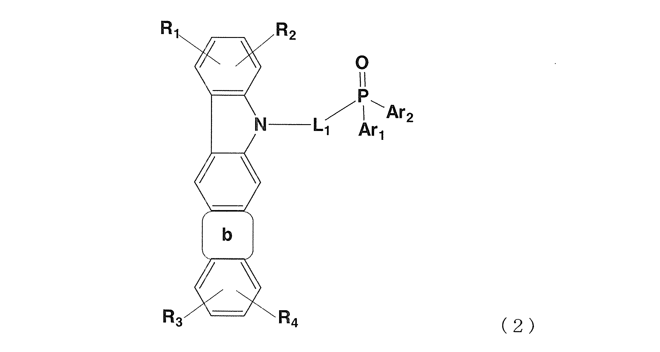
- the compound for organic electroluminescence device represented by the general formula (1) includes a compound represented by the following general formula (2), and the compound represented by the general formula (2) includes the following general formula (3).
- the ring b, Ar 1 , Ar 2 , Ar 5 , Ar 6 , R 1 to R 4 , L 1 , L 3 are the ring b, Ar 1 , Ar 2 , Ar 5 , Ar in the general formula (1). 6 , R 1 to R 4 , L 1 and L 3 have the same meaning.
- Ar 1 , Ar 2 , Ar 5 , Ar 6 , R 1 to R 4 , L 1 , L 3 , n are Ar 1 , Ar 2 , Ar 5 , Ar 6 , R 1 in the general formula (1).
- ⁇ Has the same meaning as R 4 , L 1 , L 3 , n.
- the present invention also relates to an organic electroluminescence device having an organic layer containing the above compound for organic electroluminescence device.
- the organic layer is at least one layer selected from a light emitting layer, a hole transport layer, a hole injection layer, an electron transport layer, an electron injection layer and a hole blocking element layer.
- the light emitting layer is an organic electroluminescent device comprising a phosphorescent dopant and a compound for an organic electroluminescent device represented by the general formula (1), (2) or (3) as a host material. is there.
- the compound for an organic EL device of the present invention is represented by the above general formula (1).
- a compound represented by the general formula (1) there is a compound represented by the above general formula (2).
- a compound represented by the said General formula (3) as a preferable compound of a compound represented by General formula (2).
- the compound represented by the general formula (1) typically has an indolocarbazole skeleton in which a carbazole ring and an indole ring are condensed. N of the carbazole ring is bonded to P ⁇ O directly or through a linking group, and P ⁇ O has a structure bonded to two Ar.
- the ring a represents an aromatic ring or a heterocyclic ring represented by the formula (a1) or (a2) fused with two adjacent rings.
- ring a is a heterocyclic ring represented by formula (a2)
- ring a ′ is condensed with an adjacent ring.
- Ring a ′ represents an aromatic ring or a heterocyclic ring represented by the formula (a1).
- X represents CR or N.
- R represents a group similar to R 1 to R 7 but is preferably hydrogen.
- Ring b represents a heterocycle represented by the formula (b1) that is condensed with two adjacent rings.
- General formula (2) and general formula (3) have a structure in which one or both of ring a and ring b in general formula (1) are specified. And the symbol same as the symbol used by General formula (1) has the same meaning. Therefore, general formula (2) and general formula (3) are understood from the description of general formula (1).
- the formulas (a1) and (a2), Ar 1 to Ar 6 represent a substituted or unsubstituted aromatic hydrocarbon group or a substituted or unsubstituted aromatic heterocyclic group.
- the unsubstituted aromatic hydrocarbon group include monovalent groups formed by removing one hydrogen atom from benzene, naphthalene, anthracene, phenanthrene, indene and the like, and more preferably a phenyl group, naphthyl. Groups.
- unsubstituted aromatic heterocyclic group examples include thiophene, thiazole, furan, oxazole, pyran, pyrrole, imidazole, pyrazole, isothiazole, isoxazole, furazane, triazole, pyridine, pyrazine, pyrimidine, pyridazine, triazine.
- L 1 to L 3 each independently represents a direct bond, a divalent linking group composed of a substituted or unsubstituted aromatic hydrocarbon group or a substituted or unsubstituted aromatic heterocyclic group, or a monovalent group.
- n is 0, L 2 or L 3 is a monovalent group, but L 2 , L 3 , and L 1 in other cases are divalent linking groups.
- the unsubstituted aromatic hydrocarbon group are monovalent or divalent formed by removing one or two hydrogen atoms from benzene, naphthalene, anthracene, phenanthrene, indene, biphenyl, terphenyl, quaterphenyl.
- unsubstituted aromatic heterocyclic group examples include thiophene, thiazole, furan, oxazole, pyran, pyrrole, imidazole, pyrazole, isothiazole, isoxazole, furazane, triazole, pyridine, pyrazine, pyrimidine, pyridazine, triazine.
- R 1 to R 7 are independently hydrogen, alkyl group, aralkyl group, alkenyl group, alkynyl group, cyano group, dialkylamino group, diarylamino group, diaralkylamino group, amino group, nitro group, acyl group, alkoxycarbonyl A group, a carboxyl group, an alkoxyl group, an alkylsulfonyl group, a haloalkyl group, a hydroxyl group, an amide group, a substituted or unsubstituted aromatic hydrocarbon group or an aromatic heterocyclic group; When two of them are adjacent, they may combine with each other to form a condensed ring.
- R 1 to R 7 are alkyl groups
- the carbon number is preferably 1 to 6, and when they are alkenyl groups or alkynyl groups, the carbon number is preferably 2 to 6, and the aralkyl group is In some cases, the carbon number is preferably 7 to 13, and in the case of a substituted or unsubstituted aromatic hydrocarbon group or aromatic heterocyclic group, the carbon number is preferably 3 to 15.
- the carbon number is preferably 2 to 10, and in the case of a diarylamino group or a diaralkylamino group alkyl, the carbon number is preferably 6 to 20, and an acyl group
- the carbon number is preferably 2 to 10
- the carbon number is preferably 1 to 6.
- a preferable substituent is a carbon number of 1 Alkyl group having 6 to 6 carbon atoms, alkoxy group having 1 to 6 carbon atoms, aryloxy group having 6 to 12 carbon atoms, alkylthio group, substituted amino group, acetyl group, phenyl group, biphenylyl group, terphenylyl group, naphthyl group, pyridyl group, Examples include pyrimidyl group, triazyl group, imidazolyl group, thienyl group, carbazolyl group and the like.
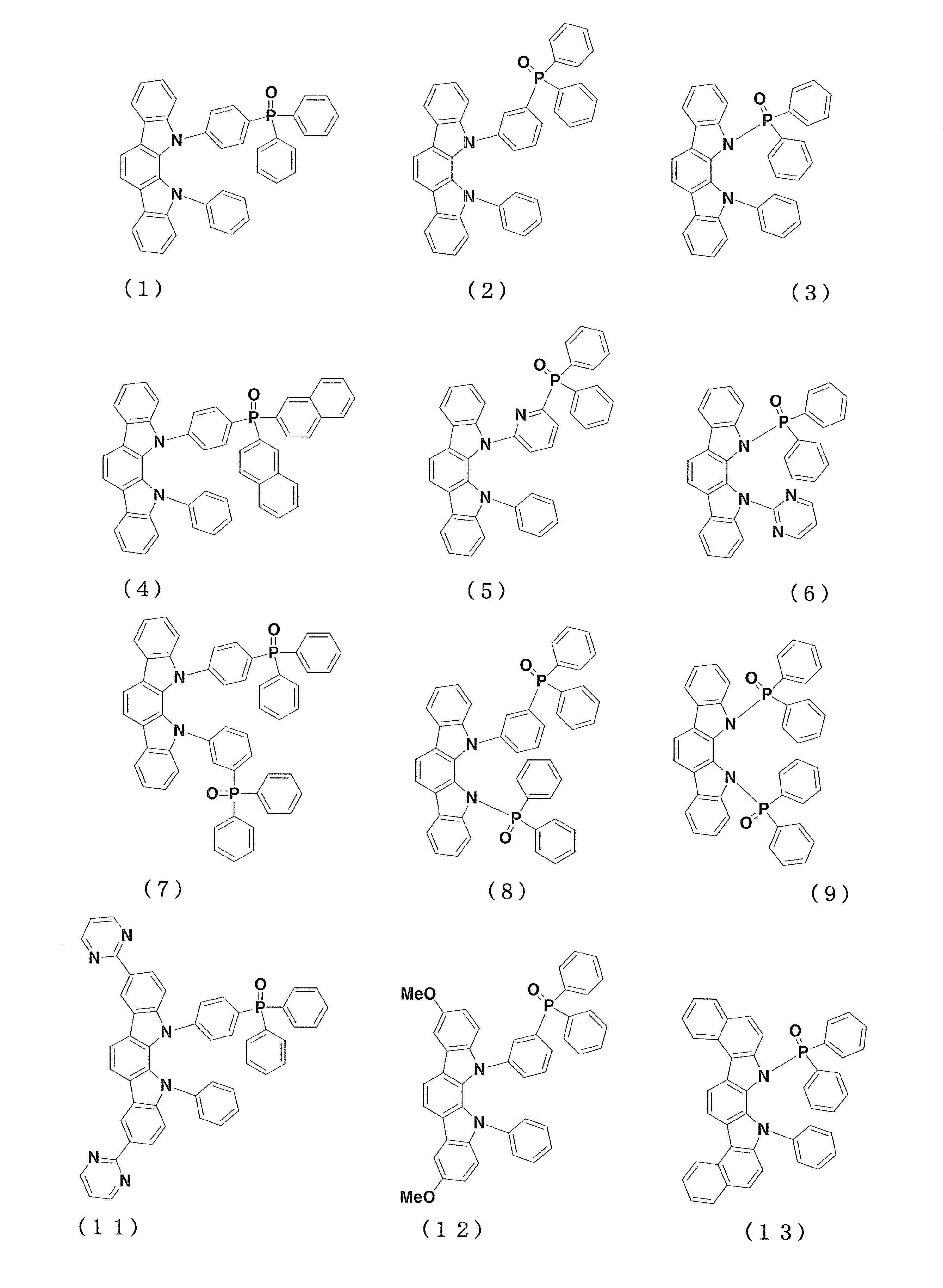
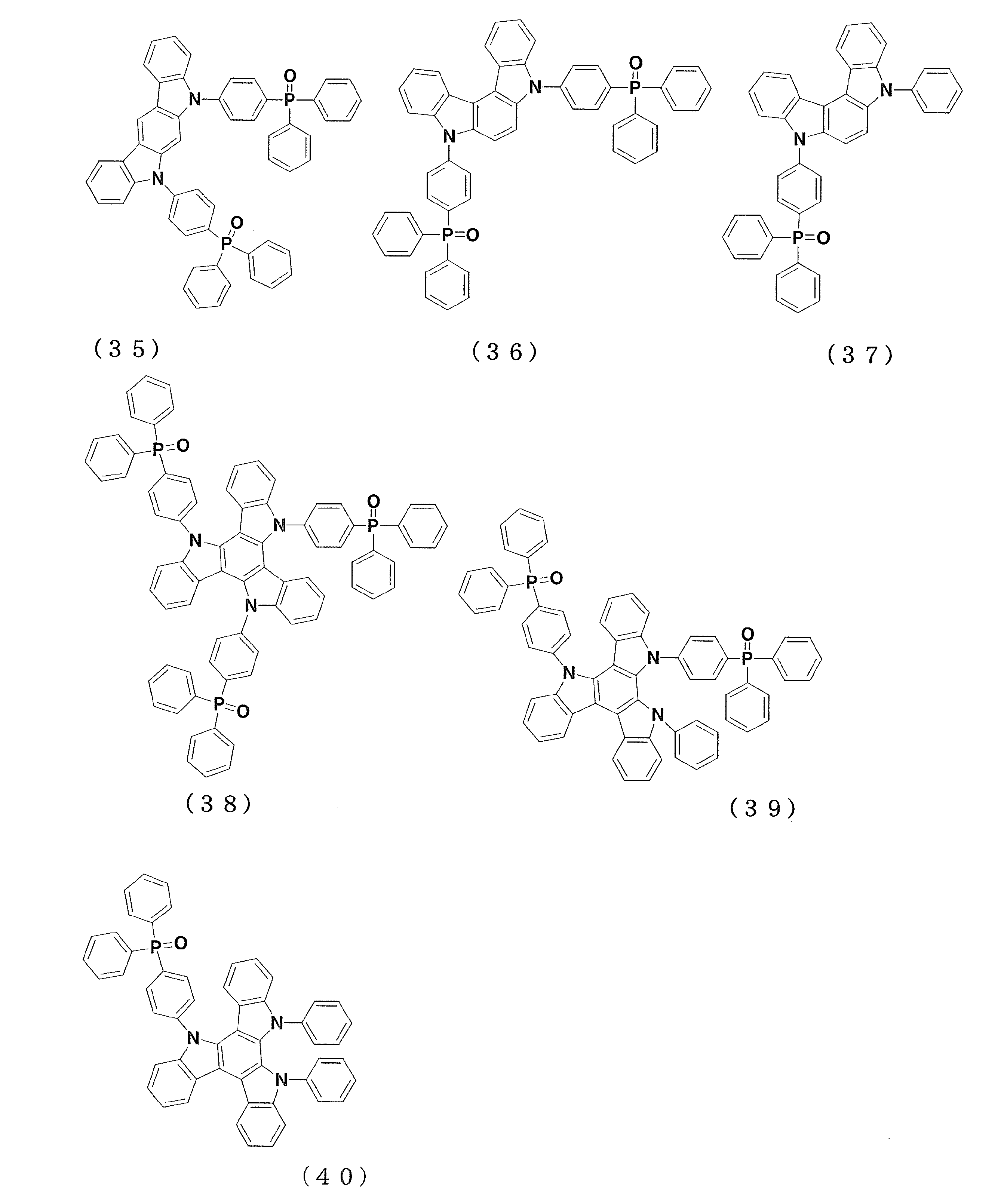
- preferred compounds include the compounds represented by the general formulas (2) and (3). Since the compound represented by the general formula (1) is a concept including the compounds represented by the above general formulas (2) and (3), these are represented by the compounds represented by the general formula (1). May be explained.
- the compound for an organic EL device of the present invention can be easily produced by a known method.
- the compound represented by the general formula (1) can be produced by the following reaction formula with reference to the synthesis example shown in Synlett, 2005, No. 1, p42-48.
- the compound for an organic electroluminescence device of the present invention gives an excellent organic electroluminescence device by being contained in the organic layer of the organic EL device.
- it may be contained in at least one organic layer selected from a light emitting layer, a hole transport layer, an electron transport layer and a hole blocking element layer. More preferably, it may be contained as a host material of a light emitting layer containing a phosphorescent dopant.
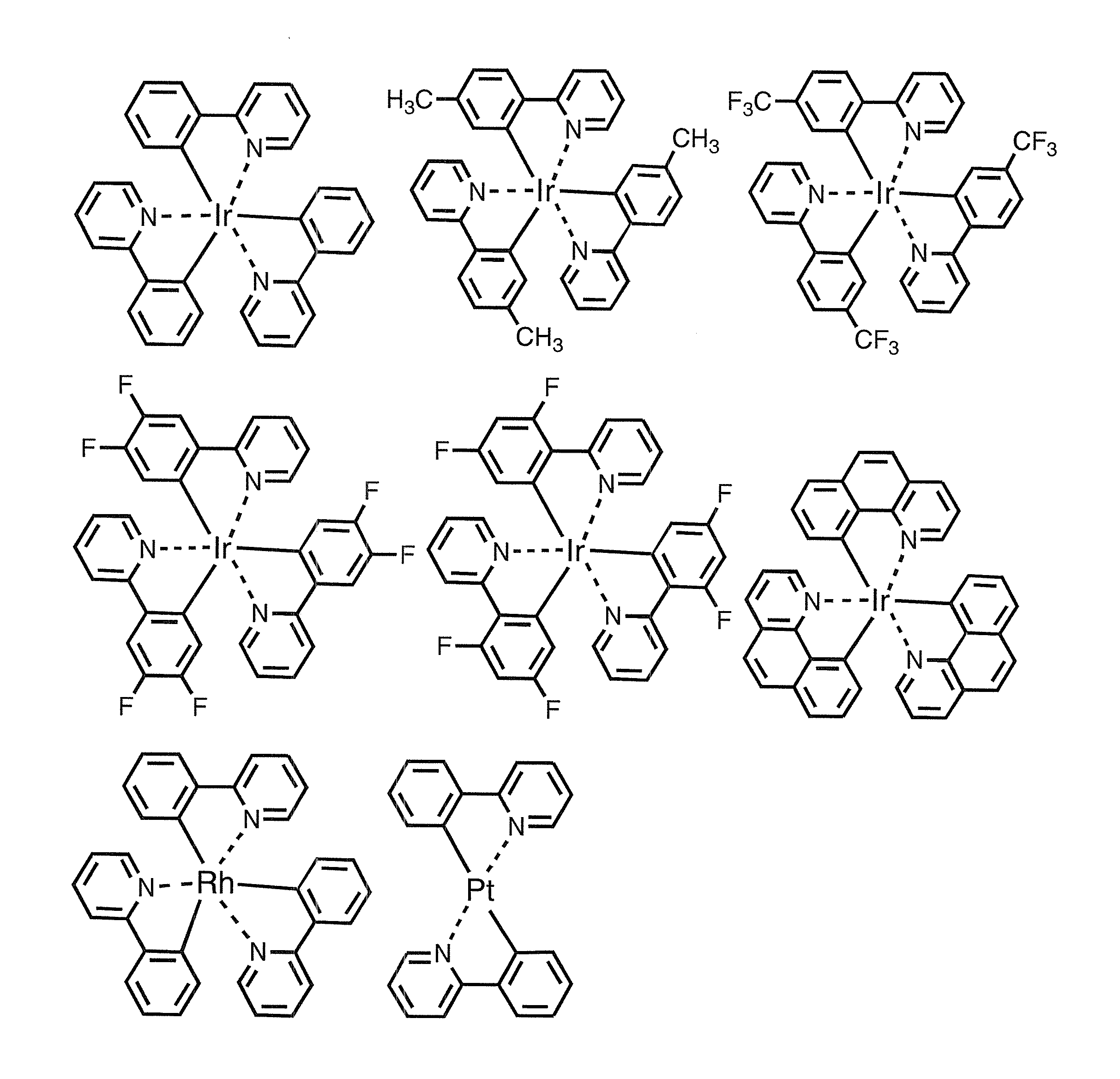
- the phosphorescent dopant material in the light emitting layer preferably contains an organometallic complex containing at least one metal selected from ruthenium, rhodium, palladium, silver, rhenium, osmium, iridium, platinum and gold.
- organometallic complexes are known in the above-mentioned patent documents and the like, and these can be selected and used.
- Preferable phosphorescent dopants include complexes such as Ir (ppy) 3 having a noble metal element such as Ir as a central metal, complexes such as Ir (bt) 2 ⁇ acac3, and complexes such as PtOEt3. Specific examples of these complexes are shown below, but are not limited to the following compounds.
- the amount of the phosphorescent dopant contained in the light emitting layer is 1 to 20% by weight, preferably 5 to 10% by weight.
- the compound of the present invention is used as the host material, and the amount contained in the light emitting layer is 50% by weight or more, preferably 80 to 95% by weight.
- the structure of the organic EL element of the present invention will be described with reference to the drawings.
- the structure of the organic EL element of the present invention is not limited to the illustrated one.
- FIG. 1 is a cross-sectional view schematically showing a structural example of a general organic EL element used in the present invention.
- 1 represents a substrate
- 2 represents an anode
- 3 represents a hole injection layer
- 4 represents a hole transport layer
- 5 represents a light emitting layer
- 6 represents an electron transport layer
- 7 represents a cathode.
- the organic EL device of the present invention has a substrate, an anode, a light emitting layer and a cathode as essential layers, but it is preferable to have a hole injecting and transporting layer and an electron injecting and transporting layer in layers other than the essential layers, and further emit light. It is preferable to have a hole blocking layer between the layer and the electron injecting and transporting layer.
- the hole injection / transport layer means either or both of a hole injection layer and a hole transport layer
- the electron injection / transport layer means either or both of an electron injection layer and an electron transport layer.
- the substrate 1 serves as a support for the organic EL element, and quartz, a glass plate, a metal plate, a metal foil, a plastic film, a sheet, or the like is used.
- a glass plate is preferable.
- the anode 2 plays a role of hole injection into the hole injection layer 3.
- the anode 2 is usually a metal such as aluminum, gold, silver, nickel, palladium, or platinum, a metal oxide such as indium and / or tin oxide (ITO), a metal halide such as copper iodide, or carbon black.
- a metal such as aluminum, gold, silver, nickel, palladium, or platinum
- a metal oxide such as indium and / or tin oxide (ITO)
- ITO indium and / or tin oxide
- metal halide such as copper iodide
- carbon black carbon black
- the light-emitting layer 5 is injected between the electrodes to which an electric field is applied, from the anode 2 to move through the hole transport layer 4 and from the cathode 7 to move through the electron transport layer 6. It is formed of a luminescent substance that emits light when excited by recombination.
- the light emitting layer 5 preferably includes a host material made of a dopant material that is a light emitting substance and the compound for an organic EL element.
- the cathode 7 serves to inject electrons into the light emitting layer 5 through the electron transport layer 6.
- the material used as the cathode 7 is preferably a metal having a low work function in order to efficiently inject electrons, and an appropriate metal such as tin, magnesium, indium, calcium, cesium, aluminum, silver, or an alloy thereof is used. Used. Specific examples include a magnesium-silver alloy, a magnesium-indium alloy, and an aluminum-lithium alloy.
- the hole injection layer 3, the hole transport layer 4, and the electron transport layer 6 are arbitrary organic layers, but the hole injection layer 3 has an efficiency of injecting holes from the anode 2 into the hole transport layer 4.
- the hole transport layer 4 and the electron transport layer 6 serve to move holes and electrons to the light emitting layer 5, respectively.
- an electron injection layer can be provided between the cathode 7 and the electron transport layer 6. The materials used for these layers are known.
- the hole injection material examples include phthalocyanine compounds such as copper phthalocyanine (CuPC), organic compounds such as polyaniline and polythiophene, and metal oxides such as vanadium oxide, ruthenium oxide, and molybdenum oxide.
- phthalocyanine compounds such as copper phthalocyanine (CuPC)
- organic compounds such as polyaniline and polythiophene
- metal oxides such as vanadium oxide, ruthenium oxide, and molybdenum oxide.
- hole transport materials include triazole derivatives, oxadiazole derivatives, imidazole derivatives, polyarylalkane derivatives, pyrazoline derivatives and pyrazolone derivatives, phenylenediamine derivatives, arylamine derivatives such as NPB, amino-substituted chalcone derivatives, oxazole derivatives, styrylanthracene.
- Derivatives, fluorenone derivatives, hydrazone derivatives, stilbene derivatives, silazane derivatives, aniline copolymers, conductive polymer oligomers, particularly thiophene oligomers, and the like can be given.
- Electron transport materials include metal complexes such as Alq3, metal complexes of 10-hydroxybenzo [h] quinoline, oxadiazole derivatives, distyrylbiphenyl derivatives, silole derivatives, 3- or 5-hydroxyflavone metal complexes, benzoxazole metals Complex, benzothiazole metal complex, trisbenzimidazolylbenzenequinoxaline compound, phenanthroline derivative, 2-t-butyl-9,10-N, N′-dicyanoanthraquinonediimine, n-type hydrogenated amorphous silicon carbide, n-type sulfide Examples include zinc and n-type zinc selenide.
- metal complexes such as Alq3, metal complexes of 10-hydroxybenzo [h] quinoline, oxadiazole derivatives, distyrylbiphenyl derivatives, silole derivatives, 3- or 5-hydroxyflavone metal complexes, benzoxazole metals
- the organic EL element of the present invention can be applied to any of a single element, an element having a structure arranged in an array, and a structure in which an anode and a cathode are arranged in an XY matrix.
- the light emitting layer contains a compound having a specific skeleton and a phosphorescent light emitting dopant, so that the light emitting efficiency is higher than that of a conventional device using light emission from a singlet state and driving.
- a device with greatly improved stability can be obtained, and excellent performance can be exhibited in application to full-color or multi-color panels.
- the filtrate was transferred to a 2000 ml separatory funnel and separated into an organic layer and an aqueous layer.
- the organic layer was washed with 500 ml of water three times, and then the obtained organic layer was dehydrated with magnesium sulfate. After magnesium sulfate was filtered off once, the solvent was distilled off under reduced pressure. Thereafter, the residue was purified by column chromatography to obtain 13.7 g (41.2 mmol, yield 40.6%) of white solid A.
- the resulting white solid A is 11-phenylindolo [2,3-a] carbazole.
- reaction solution was gradually added to 1500 g of stirring water, and the precipitated crystals were collected by filtration.
- the crystals collected by filtration were reslurried twice with 300 g of water, and the filtrate was dried under reduced pressure. 16.2 g (0.030 mol, yield 80.0%) of pale yellowish white powder was obtained.
- 120 g of chloroform was added and stirred for 1 hour, and the crystals were collected by filtration. Thereafter, the obtained organic layer was dehydrated with magnesium sulfate, and after magnesium sulfate was filtered off, the solvent was distilled off under reduced pressure.
- Example 2 an organic EL element having a configuration in which an electron injection layer was added was prepared. Each thin film was laminated at a vacuum degree of 4.0 ⁇ 10 ⁇ 4 Pa by a vacuum deposition method on a glass substrate on which an anode made of ITO having a thickness of 150 nm was formed. First, copper phthalocyanine (CuPC) was formed to a thickness of 20 nm on ITO as a hole injection layer. Next, NPB was formed to a thickness of 40 nm as a hole transport layer.
- CuPC copper phthalocyanine
- compound 3 as a host material of the light emitting layer and Ir (ppy) 3 as a dopant were co-deposited from different vapor deposition sources to form a light emitting layer having a thickness of 35 nm.
- concentration of Ir (ppy) 3 was 7.0 wt%.
- Alq3 was formed to a thickness of 40 nm as an electron transport layer.
- lithium fluoride (LiF) was formed to a thickness of 0.5 nm as an electron injection layer on the electron transport layer.
- aluminum (Al) was formed as an electrode to a thickness of 170 nm, and an organic EL element was produced.
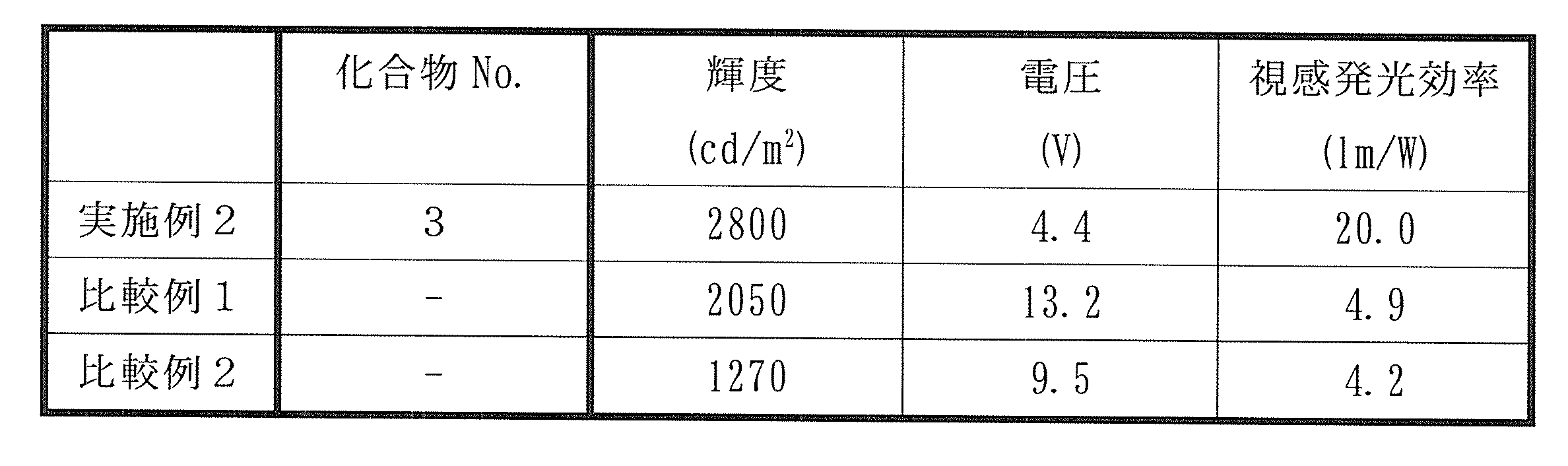
- the organic EL element had light emission characteristics as shown in Table 1.
- Table 1 the luminance, voltage, and luminous efficiency show values at 10 mA / cm 2 .
- the maximum wavelength of the device emission spectrum was 517 nm, indicating that light emission from Ir (ppy) 3 was obtained.
- Comparative Example 1 An organic EL device was produced in the same manner as in Example 2 except that HMTPD was used as the hole transport layer and TAZ was used as the host material of the light emitting layer.
- Table 1 the luminance, voltage, and luminous efficiency show values at 10 mA / cm 2 .
- the maximum wavelength of the device emission spectrum was 517 nm, indicating that light emission from Ir (ppy) 3 was obtained.
- Comparative Example 2 An organic EL device was produced in the same manner as in Example 2 except that TAZ was used as the host material for the light emitting layer. The maximum wavelength of the device emission spectrum was 517 nm, indicating that light emission from Ir (ppy) 3 was obtained.
- the organic EL element of the present invention can emit light with high luminance and high efficiency at a low voltage.
- the organic EL device according to the present invention is a flat panel display (for example, for OA computers or wall-mounted televisions), an in-vehicle display device, a light source utilizing characteristics of a mobile phone display or a surface light emitter (for example, a light source of a copying machine, a liquid crystal). It can be applied to backlight sources for displays and instruments, display panels, and indicator lights, and its technical value is great.
Landscapes
- Chemical & Material Sciences (AREA)
- Organic Chemistry (AREA)
- Engineering & Computer Science (AREA)
- Materials Engineering (AREA)
- Health & Medical Sciences (AREA)
- Life Sciences & Earth Sciences (AREA)
- Biochemistry (AREA)
- General Health & Medical Sciences (AREA)
- Molecular Biology (AREA)
- Physics & Mathematics (AREA)
- Spectroscopy & Molecular Physics (AREA)
- Optics & Photonics (AREA)
- Electroluminescent Light Sources (AREA)
Abstract
Description








APCI-MS, m/z 533 [M+H]+、融点258℃。
図1において、電子注入層を追加した構成の有機EL素子を作成した。膜厚150nmのITOからなる陽極が形成されたガラス基板上に、各薄膜を真空蒸着法にて、真空度4.0×10⁻⁴ Paで積層させた。まず、ITO 上に正孔注入層として、銅フタロシアニン(CuPC) を 20 nm の厚さに形成した。次に、正孔輸送層として NPB を 40 nm の厚さに形成した。次に、正孔輸送層上に、発光層のホスト材料として化合物3と、ドーパントとしてIr(ppy)3とを異なる蒸着源から、共蒸着し、35nmの厚さに発光層を形成した。この時、Ir(ppy)3の濃度は7.0 wt%であった。次に、電子輸送層としてAlq3を40nmの厚さに形成した。更に、電子輸送層上に、電子注入層としてフッ化リチウム(LiF)を0.5nmの厚さに形成した。最後に、電子注入層上に、電極としてアルミニウム(Al)を170nmの厚さに形成し、有機EL素子を作成した。
正孔輸送層としてHMTPDを用い、発光層のホスト材料としてTAZを用いた以外は実施例2と同様にして有機EL素子を作成した。表1において、輝度、電圧及び発光効率は、10mA/cm2での値を示す。なお、素子発光スペクトルの極大波長は517 nmであり、Ir(ppy)3からの発光が得られていることがわかった。
発光層のホスト材料として、TAZを用いた以外は実施例2と同様にして有機EL素子を作成した。なお、素子発光スペクトルの極大波長は517 nmであり、Ir(ppy)3からの発光が得られていることがわかった。
Claims (8)
- 下記一般式(1)で示される有機電界発光素子用化合物。
ここで、環aは、2つの隣接環と縮合する式(a1)又は(a2)で表される芳香環又は複素環を示し、環a'は、3つの隣接環と縮合する式(a1)で表される芳香環又は複素環を示し、環bは、2つの隣接環と縮合する式(b1)で表される複素環を示す。Xは独立に、CR又はNを示す。Ar1~Ar6は独立に、置換若しくは未置換の芳香族炭化水素基又は芳香族複素環基を示す。R及びR1~R7は独立に、水素、アルキル基、アラルキル基、アルケニル基、アルキニル基、シアノ基、ジアルキルアミノ基、ジアリールアミノ基、ジアラルキルアミノ基、アミノ基、ニトロ基、アシル基、アルコキシカルボニル基、カルボキシル基、アルコキシル基、アルキルスルホニル基、ハロアルキル基、水酸基、アミド基、置換若しくは未置換の芳香族炭化水素基又は芳香族複素環基を示し、そのうちの二つが隣接する場合、互いに結合して環を形成してもよい。L1~L3は独立に直接結合、又は置換若しくは未置換の芳香族炭化水素基若しくは芳香族複素環基を表す。nは独立に、0又は1の整数を表す。
- 下記一般式(2)で示される請求項1に記載の有機電界発光素子用化合物。
ここで、環b、Ar1、Ar2、R1~R4、及びL1は、一般式(1)の環b、Ar1、Ar2、R1~R4、及びL1と同じ意味を有する。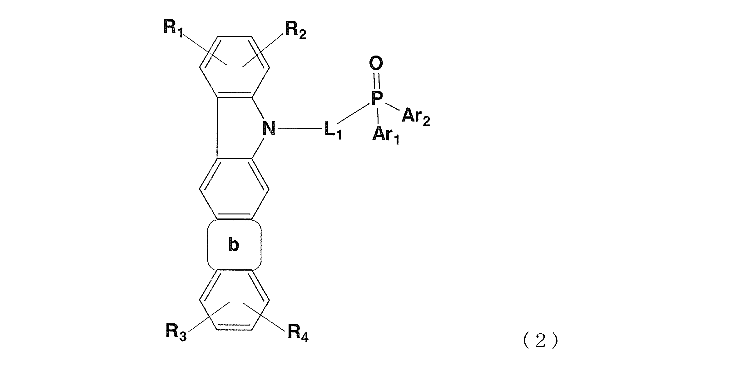
- 下記一般式(3)で示される請求項1に記載の有機電界発光素子用化合物。
ここで、Ar1、Ar2、Ar5、Ar6、R1~R4、L1、L3、及びnは、一般式(1)のAr1、Ar2、Ar5、Ar6、R1~R4、L1、L3、及びnと同じ意味を有する。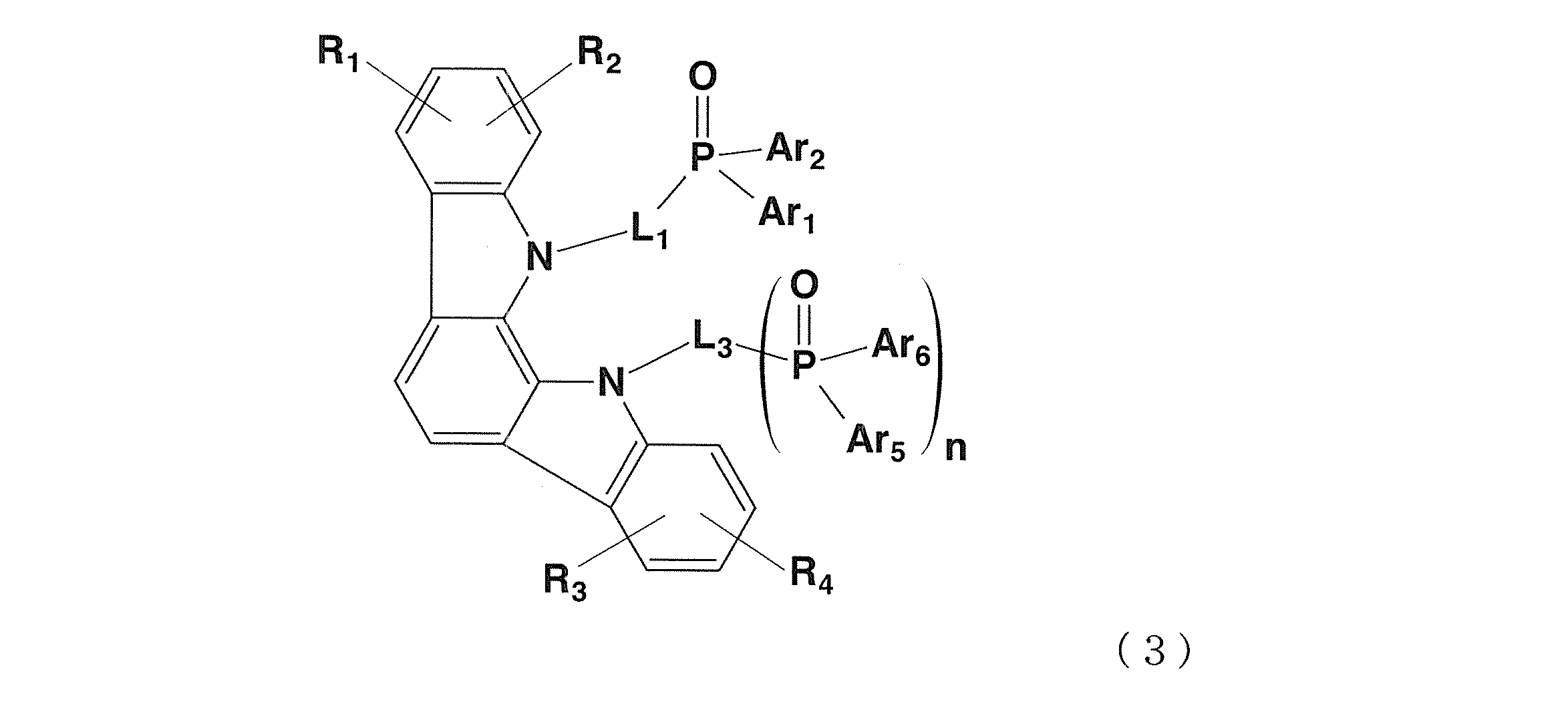
- 一般式(1)において、Ar1~Ar6が独立して、置換若しくは未置換のフェニル基、又は置換若しくは未置換の炭素数2~5の芳香族複素環基である請求項1に記載の有機電解発光素子用化合物。
- 一般式(1)において、R1~R5が独立して、水素、置換若しくは未置換の炭素数5~18の芳香族炭化水素基又は炭素数3~17の芳香族複素環基である請求項1に記載の有機電解発光素子用化合物。
- 請求項1~5のいずれかに記載の有機電界発光素子用化合物を含む有機層を有する有機電界発光素子。
- 有機電界発光素子用化合物を含む有機層が、発光層、正孔輸送層、正孔注入層、電子輸送層、電子注入層及び正孔阻止素子層から選ばれる少なくとも一つの層である請求項6に記載の有機電界発光素子。
- 有機電界発光素子用化合物を含む有機層が発光層であり、該発光層が燐光発光性ドーパントと該有機電界発光素子用化合物をホスト材料として含有する請求項6に記載の有機電界発光素子。
Priority Applications (4)
| Application Number | Priority Date | Filing Date | Title |
|---|---|---|---|
| US12/991,167 US8703302B2 (en) | 2008-05-08 | 2009-04-30 | Indolocarbazole derivative with aromatic phosphne oxide group for organic electroluminescent device and organic electroluminescent device containing same |
| EP09742710.8A EP2293357B1 (en) | 2008-05-08 | 2009-04-30 | Compound for organic electroluminescent device and organic electroluminescent device |
| JP2010511061A JP5200099B2 (ja) | 2008-05-08 | 2009-04-30 | 有機電界発光素子用化合物及び有機電界発光素子 |
| CN2009801164326A CN102017221B (zh) | 2008-05-08 | 2009-04-30 | 有机场致发光元件用化合物及有机场致发光元件 |
Applications Claiming Priority (2)
| Application Number | Priority Date | Filing Date | Title |
|---|---|---|---|
| JP2008-122060 | 2008-05-08 | ||
| JP2008122060 | 2008-05-08 |
Publications (1)
| Publication Number | Publication Date |
|---|---|
| WO2009136586A1 true WO2009136586A1 (ja) | 2009-11-12 |
Family
ID=41264641
Family Applications (1)
| Application Number | Title | Priority Date | Filing Date |
|---|---|---|---|
| PCT/JP2009/058451 Ceased WO2009136586A1 (ja) | 2008-05-08 | 2009-04-30 | 有機電界発光素子用化合物及び有機電界発光素子 |
Country Status (7)
| Country | Link |
|---|---|
| US (1) | US8703302B2 (ja) |
| EP (1) | EP2293357B1 (ja) |
| JP (1) | JP5200099B2 (ja) |
| KR (1) | KR101571114B1 (ja) |
| CN (1) | CN102017221B (ja) |
| TW (1) | TWI457417B (ja) |
| WO (1) | WO2009136586A1 (ja) |
Cited By (6)
| Publication number | Priority date | Publication date | Assignee | Title |
|---|---|---|---|---|
| WO2010098386A1 (ja) * | 2009-02-27 | 2010-09-02 | 新日鐵化学株式会社 | 有機電界発光素子 |
| WO2014024856A1 (ja) * | 2012-08-07 | 2014-02-13 | 国立大学法人九州大学 | 有機エレクトロルミネッセンス素子、並びに、それに用いる化合物、キャリア輸送材料およびホスト材料 |
| JP2015120702A (ja) * | 2009-03-20 | 2015-07-02 | ローム・アンド・ハース・エレクトロニック・マテリアルズ・コリア・リミテッド | 新規有機電界発光化合物およびこれを使用する有機電界発光素子 |
| JP2015528445A (ja) * | 2012-08-17 | 2015-09-28 | ドゥーサン コーポレイション | 新規な化合物及びこれを含む有機電界発光素子 |
| KR101753485B1 (ko) | 2014-10-27 | 2017-07-04 | 주식회사 엘지화학 | 화합물 및 이를 포함하는 유기 발광 소자 |
| JP2018056536A (ja) * | 2016-09-23 | 2018-04-05 | 日本放送協会 | 有機エレクトロルミネッセンス素子 |
Families Citing this family (27)
| Publication number | Priority date | Publication date | Assignee | Title |
|---|---|---|---|---|
| ES2691646T3 (es) | 2005-07-15 | 2018-11-28 | Micell Technologies, Inc. | Revestimientos poliméricos que contienen polvo de fármaco de morfología controlada |
| WO2007011708A2 (en) | 2005-07-15 | 2007-01-25 | Micell Technologies, Inc. | Stent with polymer coating containing amorphous rapamycin |
| CA2996768C (en) | 2006-04-26 | 2020-12-08 | Micell Technologies, Inc. | Coatings containing multiple drugs |
| JP5336382B2 (ja) | 2006-10-23 | 2013-11-06 | ミセル テクノロジーズ、インコーポレイテッド | コーティングの間に基板を荷電するためのホルダー |
| US11426494B2 (en) | 2007-01-08 | 2022-08-30 | MT Acquisition Holdings LLC | Stents having biodegradable layers |
| CN101711137B (zh) | 2007-01-08 | 2014-10-22 | 米歇尔技术公司 | 具有可生物降解层的支架 |
| CN101815540B (zh) | 2007-05-25 | 2015-08-19 | 米歇尔技术公司 | 用于医疗器材涂层的聚合物膜 |
| CA2721832C (en) | 2008-04-17 | 2018-08-07 | Micell Technologies, Inc. | Stents having bioabsorbable layers |
| WO2010009335A1 (en) | 2008-07-17 | 2010-01-21 | Micell Technologies, Inc. | Drug delivery medical device |
| US8834913B2 (en) | 2008-12-26 | 2014-09-16 | Battelle Memorial Institute | Medical implants and methods of making medical implants |
| CN102481195B (zh) | 2009-04-01 | 2015-03-25 | 米歇尔技术公司 | 涂覆支架 |
| EP3366326A1 (en) | 2009-04-17 | 2018-08-29 | Micell Technologies, Inc. | Stents having controlled elution |
| EP2453834A4 (en) | 2009-07-16 | 2014-04-16 | Micell Technologies Inc | MEDICAL DEVICE DISPENSING MEDICINE |
| EP2531140B1 (en) | 2010-02-02 | 2017-11-01 | Micell Technologies, Inc. | Stent and stent delivery system with improved deliverability |
| US8795762B2 (en) | 2010-03-26 | 2014-08-05 | Battelle Memorial Institute | System and method for enhanced electrostatic deposition and surface coatings |
| WO2011133655A1 (en) | 2010-04-22 | 2011-10-27 | Micell Technologies, Inc. | Stents and other devices having extracellular matrix coating |
| WO2012009684A2 (en) | 2010-07-16 | 2012-01-19 | Micell Technologies, Inc. | Drug delivery medical device |
| WO2012166819A1 (en) | 2011-05-31 | 2012-12-06 | Micell Technologies, Inc. | System and process for formation of a time-released, drug-eluting transferable coating |
| US10117972B2 (en) | 2011-07-15 | 2018-11-06 | Micell Technologies, Inc. | Drug delivery medical device |
| US10188772B2 (en) | 2011-10-18 | 2019-01-29 | Micell Technologies, Inc. | Drug delivery medical device |
| CN110269959A (zh) | 2013-03-12 | 2019-09-24 | 脉胜医疗技术公司 | 可生物吸收的生物医学植入物 |
| KR102081689B1 (ko) * | 2013-03-15 | 2020-02-26 | 덕산네오룩스 주식회사 | 유기전기 소자용 화합물, 이를 이용한 유기전기소자 및 그 전자 장치 |
| WO2014186532A1 (en) | 2013-05-15 | 2014-11-20 | Micell Technologies, Inc. | Bioabsorbable biomedical implants |
| CN104610353B (zh) * | 2015-02-06 | 2019-06-21 | 中国科学院福建物质结构研究所 | 一种离子型磷光Au4Ag2配合物及其制备方法和用途 |
| CN104892685B (zh) * | 2015-04-13 | 2018-09-28 | 中国科学院福建物质结构研究所 | 一种离子型磷光PtM2配合物及其制备方法和用途 |
| CN106432238A (zh) * | 2016-09-07 | 2017-02-22 | 西安近代化学研究所 | 一种具有四氮并九环结构的稠环化合物及其制备方法 |
| KR102016737B1 (ko) | 2017-12-29 | 2019-09-02 | 인하대학교 산학협력단 | 삼각형 메쉬 기반 컴퓨터 생성 홀로그램의 제공 장치 및 방법 |
Citations (11)
| Publication number | Priority date | Publication date | Assignee | Title |
|---|---|---|---|---|
| JPS6462650A (en) | 1987-09-03 | 1989-03-09 | Fuji Xerox Co Ltd | Method for polishing surface of electrophotographic sensitive body |
| JPH11144866A (ja) * | 1997-11-05 | 1999-05-28 | Toray Ind Inc | 発光素子 |
| JPH11162650A (ja) * | 1997-10-02 | 1999-06-18 | Xerox Corp | エレクトロルミネセントデバイス |
| JPH11176578A (ja) | 1997-10-02 | 1999-07-02 | Xerox Corp | インドロカルバゾールを用いたエレクトロルミネセントデバイス |
| JP2001313178A (ja) | 2000-04-28 | 2001-11-09 | Pioneer Electronic Corp | 有機エレクトロルミネッセンス素子 |
| JP2002352957A (ja) | 2001-05-23 | 2002-12-06 | Honda Motor Co Ltd | 有機エレクトロルミネッセンス素子 |
| JP2003515897A (ja) | 1999-12-01 | 2003-05-07 | ザ、トラスティーズ オブ プリンストン ユニバーシティ | 有機led用燐光性ドーパントとしての式l2mxの錯体 |
| JP2007109988A (ja) * | 2005-10-17 | 2007-04-26 | Toyo Ink Mfg Co Ltd | 有機エレクトロルミネッセンス素子 |
| JP2007129206A (ja) | 2005-10-04 | 2007-05-24 | Fujifilm Corp | 有機電界発光素子 |
| WO2007063796A1 (ja) | 2005-12-01 | 2007-06-07 | Nippon Steel Chemical Co., Ltd. | 有機電界発光素子 |
| WO2007137725A1 (de) | 2006-05-31 | 2007-12-06 | Merck Patent Gmbh | Neue materialien für organische elektrolumineszenzvorrichtungen |
Family Cites Families (3)
| Publication number | Priority date | Publication date | Assignee | Title |
|---|---|---|---|---|
| WO2006098229A1 (ja) * | 2005-03-15 | 2006-09-21 | Nippon Steel Chemical Co., Ltd. | インドロカルバゾール誘導体を含有する電極活物質 |
| DE102005023437A1 (de) * | 2005-05-20 | 2006-11-30 | Merck Patent Gmbh | Verbindungen für organische elektronische Vorrichtungen |
| WO2007063754A1 (ja) * | 2005-12-01 | 2007-06-07 | Nippon Steel Chemical Co., Ltd. | 有機電界発光素子用化合物及び有機電界発光素子 |
-
2009
- 2009-04-30 WO PCT/JP2009/058451 patent/WO2009136586A1/ja not_active Ceased
- 2009-04-30 JP JP2010511061A patent/JP5200099B2/ja not_active Expired - Fee Related
- 2009-04-30 EP EP09742710.8A patent/EP2293357B1/en not_active Not-in-force
- 2009-04-30 US US12/991,167 patent/US8703302B2/en not_active Expired - Fee Related
- 2009-04-30 KR KR1020107026682A patent/KR101571114B1/ko not_active Expired - Fee Related
- 2009-04-30 CN CN2009801164326A patent/CN102017221B/zh not_active Expired - Fee Related
- 2009-05-06 TW TW098115006A patent/TWI457417B/zh not_active IP Right Cessation
Patent Citations (11)
| Publication number | Priority date | Publication date | Assignee | Title |
|---|---|---|---|---|
| JPS6462650A (en) | 1987-09-03 | 1989-03-09 | Fuji Xerox Co Ltd | Method for polishing surface of electrophotographic sensitive body |
| JPH11162650A (ja) * | 1997-10-02 | 1999-06-18 | Xerox Corp | エレクトロルミネセントデバイス |
| JPH11176578A (ja) | 1997-10-02 | 1999-07-02 | Xerox Corp | インドロカルバゾールを用いたエレクトロルミネセントデバイス |
| JPH11144866A (ja) * | 1997-11-05 | 1999-05-28 | Toray Ind Inc | 発光素子 |
| JP2003515897A (ja) | 1999-12-01 | 2003-05-07 | ザ、トラスティーズ オブ プリンストン ユニバーシティ | 有機led用燐光性ドーパントとしての式l2mxの錯体 |
| JP2001313178A (ja) | 2000-04-28 | 2001-11-09 | Pioneer Electronic Corp | 有機エレクトロルミネッセンス素子 |
| JP2002352957A (ja) | 2001-05-23 | 2002-12-06 | Honda Motor Co Ltd | 有機エレクトロルミネッセンス素子 |
| JP2007129206A (ja) | 2005-10-04 | 2007-05-24 | Fujifilm Corp | 有機電界発光素子 |
| JP2007109988A (ja) * | 2005-10-17 | 2007-04-26 | Toyo Ink Mfg Co Ltd | 有機エレクトロルミネッセンス素子 |
| WO2007063796A1 (ja) | 2005-12-01 | 2007-06-07 | Nippon Steel Chemical Co., Ltd. | 有機電界発光素子 |
| WO2007137725A1 (de) | 2006-05-31 | 2007-12-06 | Merck Patent Gmbh | Neue materialien für organische elektrolumineszenzvorrichtungen |
Non-Patent Citations (4)
| Title |
|---|
| ARCHIV DER PHARMAZIE, 1987, pages 280 - 282 |
| SAPOCHAK L.S. ET AL.: "Inductive Effects of Disphenylphosphoryl Moieties on Carbazole Host Materials: Design Rules for Blue Electrophosphorescent Organic Light-Emitting Devices", J PHYS.CHEM. C, vol. 112, 2008, pages 7989 - 7996, XP008138908 * |
| See also references of EP2293357A4 |
| SYNLETT., no. 1, 2005, pages 42 - 48 |
Cited By (9)
| Publication number | Priority date | Publication date | Assignee | Title |
|---|---|---|---|---|
| WO2010098386A1 (ja) * | 2009-02-27 | 2010-09-02 | 新日鐵化学株式会社 | 有機電界発光素子 |
| JPWO2010098386A1 (ja) * | 2009-02-27 | 2012-09-06 | 新日鐵化学株式会社 | 有機電界発光素子 |
| US8722208B2 (en) | 2009-02-27 | 2014-05-13 | Nippon Steel & Sumikin Chemical Co., Ltd. | Organic electroluminescent device |
| JP2015120702A (ja) * | 2009-03-20 | 2015-07-02 | ローム・アンド・ハース・エレクトロニック・マテリアルズ・コリア・リミテッド | 新規有機電界発光化合物およびこれを使用する有機電界発光素子 |
| WO2014024856A1 (ja) * | 2012-08-07 | 2014-02-13 | 国立大学法人九州大学 | 有機エレクトロルミネッセンス素子、並びに、それに用いる化合物、キャリア輸送材料およびホスト材料 |
| JP2015528445A (ja) * | 2012-08-17 | 2015-09-28 | ドゥーサン コーポレイション | 新規な化合物及びこれを含む有機電界発光素子 |
| US9837618B2 (en) | 2012-08-17 | 2017-12-05 | Doosan Corporation | Compound and organic electroluminescence device including thesame |
| KR101753485B1 (ko) | 2014-10-27 | 2017-07-04 | 주식회사 엘지화학 | 화합물 및 이를 포함하는 유기 발광 소자 |
| JP2018056536A (ja) * | 2016-09-23 | 2018-04-05 | 日本放送協会 | 有機エレクトロルミネッセンス素子 |
Also Published As
| Publication number | Publication date |
|---|---|
| US8703302B2 (en) | 2014-04-22 |
| JP5200099B2 (ja) | 2013-05-15 |
| TW201005072A (en) | 2010-02-01 |
| US20110057184A1 (en) | 2011-03-10 |
| CN102017221A (zh) | 2011-04-13 |
| EP2293357A4 (en) | 2013-08-28 |
| EP2293357A1 (en) | 2011-03-09 |
| KR20110007233A (ko) | 2011-01-21 |
| TWI457417B (zh) | 2014-10-21 |
| CN102017221B (zh) | 2013-01-02 |
| EP2293357B1 (en) | 2014-12-10 |
| JPWO2009136586A1 (ja) | 2011-09-08 |
| KR101571114B1 (ko) | 2015-11-23 |
Similar Documents
| Publication | Publication Date | Title |
|---|---|---|
| JP5200099B2 (ja) | 有機電界発光素子用化合物及び有機電界発光素子 | |
| JP4819181B2 (ja) | 有機電界発光素子用化合物及び有機電界発光素子 | |
| JP5215481B2 (ja) | 有機電界発光素子 | |
| JP4593631B2 (ja) | 有機電界発光素子用化合物及び有機電界発光素子 | |
| JP4870245B2 (ja) | 燐光発光素子用材料及びこれを用いた有機電界発光素子 | |
| KR101005160B1 (ko) | 유기 전계 발광 소자용 화합물 및 유기 전계 발광 소자 | |
| JP5399418B2 (ja) | 有機電界発光素子 | |
| CN102918134B (zh) | 有机电致发光化合物和使用该化合物的有机电致发光器件 | |
| CN103098253B (zh) | 有机电致发光元件 | |
| JP5421242B2 (ja) | 有機電界発光素子用化合物及びこれを用いた有機電界発光素子 | |
| JPWO2010113726A1 (ja) | 燐光発光素子用材料及びこれを用いた有機電界発光素子 | |
| JPWO2011081061A1 (ja) | 有機電界発光素子 | |
| JPWO2010113761A1 (ja) | 有機電界発光素子 |
Legal Events
| Date | Code | Title | Description |
|---|---|---|---|
| WWE | Wipo information: entry into national phase |
Ref document number: 200980116432.6 Country of ref document: CN |
|
| 121 | Ep: the epo has been informed by wipo that ep was designated in this application |
Ref document number: 09742710 Country of ref document: EP Kind code of ref document: A1 |
|
| WWE | Wipo information: entry into national phase |
Ref document number: 2010511061 Country of ref document: JP |
|
| WWE | Wipo information: entry into national phase |
Ref document number: 12991167 Country of ref document: US |
|
| NENP | Non-entry into the national phase |
Ref country code: DE |
|
| WWE | Wipo information: entry into national phase |
Ref document number: 2009742710 Country of ref document: EP |
|
| ENP | Entry into the national phase |
Ref document number: 20107026682 Country of ref document: KR Kind code of ref document: A |