WO2009139153A1 - 半導体部品の製造方法および半導体部品 - Google Patents
半導体部品の製造方法および半導体部品 Download PDFInfo
- Publication number
- WO2009139153A1 WO2009139153A1 PCT/JP2009/002076 JP2009002076W WO2009139153A1 WO 2009139153 A1 WO2009139153 A1 WO 2009139153A1 JP 2009002076 W JP2009002076 W JP 2009002076W WO 2009139153 A1 WO2009139153 A1 WO 2009139153A1
- Authority
- WO
- WIPO (PCT)
- Prior art keywords
- circuit board
- semiconductor component
- manufacturing
- component according
- flux activity
- Prior art date
- Legal status (The legal status is an assumption and is not a legal conclusion. Google has not performed a legal analysis and makes no representation as to the accuracy of the status listed.)
- Ceased
Links
Images


Classifications
-
- H—ELECTRICITY
- H10—SEMICONDUCTOR DEVICES; ELECTRIC SOLID-STATE DEVICES NOT OTHERWISE PROVIDED FOR
- H10W—GENERIC PACKAGES, INTERCONNECTIONS, CONNECTORS OR OTHER CONSTRUCTIONAL DETAILS OF DEVICES COVERED BY CLASS H10
- H10W90/00—Package configurations
- H10W90/701—Package configurations characterised by the relative positions of pads or connectors relative to package parts
-
- C—CHEMISTRY; METALLURGY
- C09—DYES; PAINTS; POLISHES; NATURAL RESINS; ADHESIVES; COMPOSITIONS NOT OTHERWISE PROVIDED FOR; APPLICATIONS OF MATERIALS NOT OTHERWISE PROVIDED FOR
- C09J—ADHESIVES; NON-MECHANICAL ASPECTS OF ADHESIVE PROCESSES IN GENERAL; ADHESIVE PROCESSES NOT PROVIDED FOR ELSEWHERE; USE OF MATERIALS AS ADHESIVES
- C09J163/00—Adhesives based on epoxy resins; Adhesives based on derivatives of epoxy resins
-
- H—ELECTRICITY
- H10—SEMICONDUCTOR DEVICES; ELECTRIC SOLID-STATE DEVICES NOT OTHERWISE PROVIDED FOR
- H10W—GENERIC PACKAGES, INTERCONNECTIONS, CONNECTORS OR OTHER CONSTRUCTIONAL DETAILS OF DEVICES COVERED BY CLASS H10
- H10W74/00—Encapsulations, e.g. protective coatings
- H10W74/01—Manufacture or treatment
- H10W74/012—Manufacture or treatment of encapsulations on active surfaces of flip-chip devices, e.g. forming underfills
-
- H—ELECTRICITY
- H10—SEMICONDUCTOR DEVICES; ELECTRIC SOLID-STATE DEVICES NOT OTHERWISE PROVIDED FOR
- H10W—GENERIC PACKAGES, INTERCONNECTIONS, CONNECTORS OR OTHER CONSTRUCTIONAL DETAILS OF DEVICES COVERED BY CLASS H10
- H10W74/00—Encapsulations, e.g. protective coatings
- H10W74/10—Encapsulations, e.g. protective coatings characterised by their shape or disposition
- H10W74/111—Encapsulations, e.g. protective coatings characterised by their shape or disposition the semiconductor body being completely enclosed
- H10W74/129—Encapsulations, e.g. protective coatings characterised by their shape or disposition the semiconductor body being completely enclosed forming a chip-scale package [CSP]
-
- H—ELECTRICITY
- H10—SEMICONDUCTOR DEVICES; ELECTRIC SOLID-STATE DEVICES NOT OTHERWISE PROVIDED FOR
- H10W—GENERIC PACKAGES, INTERCONNECTIONS, CONNECTORS OR OTHER CONSTRUCTIONAL DETAILS OF DEVICES COVERED BY CLASS H10
- H10W74/00—Encapsulations, e.g. protective coatings
- H10W74/10—Encapsulations, e.g. protective coatings characterised by their shape or disposition
- H10W74/15—Encapsulations, e.g. protective coatings characterised by their shape or disposition on active surfaces of flip-chip devices, e.g. underfills
-
- H—ELECTRICITY
- H05—ELECTRIC TECHNIQUES NOT OTHERWISE PROVIDED FOR
- H05K—PRINTED CIRCUITS; CASINGS OR CONSTRUCTIONAL DETAILS OF ELECTRIC APPARATUS; MANUFACTURE OF ASSEMBLAGES OF ELECTRICAL COMPONENTS
- H05K2201/00—Indexing scheme relating to printed circuits covered by H05K1/00
- H05K2201/10—Details of components or other objects attached to or integrated in a printed circuit board
- H05K2201/10227—Other objects, e.g. metallic pieces
- H05K2201/10378—Interposers
-
- H—ELECTRICITY
- H05—ELECTRIC TECHNIQUES NOT OTHERWISE PROVIDED FOR
- H05K—PRINTED CIRCUITS; CASINGS OR CONSTRUCTIONAL DETAILS OF ELECTRIC APPARATUS; MANUFACTURE OF ASSEMBLAGES OF ELECTRICAL COMPONENTS
- H05K2201/00—Indexing scheme relating to printed circuits covered by H05K1/00
- H05K2201/10—Details of components or other objects attached to or integrated in a printed circuit board
- H05K2201/10613—Details of electrical connections of non-printed components, e.g. special leads
- H05K2201/10621—Components characterised by their electrical contacts
- H05K2201/10674—Flip chip
-
- H—ELECTRICITY
- H05—ELECTRIC TECHNIQUES NOT OTHERWISE PROVIDED FOR
- H05K—PRINTED CIRCUITS; CASINGS OR CONSTRUCTIONAL DETAILS OF ELECTRIC APPARATUS; MANUFACTURE OF ASSEMBLAGES OF ELECTRICAL COMPONENTS
- H05K3/00—Apparatus or processes for manufacturing printed circuits
- H05K3/0011—Working of insulating substrates or insulating layers
- H05K3/0044—Mechanical working of the substrate, e.g. drilling or punching
- H05K3/0052—Depaneling, i.e. dividing a panel into circuit boards; Working of the edges of circuit boards
-
- H—ELECTRICITY
- H10—SEMICONDUCTOR DEVICES; ELECTRIC SOLID-STATE DEVICES NOT OTHERWISE PROVIDED FOR
- H10P—GENERIC PROCESSES OR APPARATUS FOR THE MANUFACTURE OR TREATMENT OF DEVICES COVERED BY CLASS H10
- H10P72/00—Handling or holding of wafers, substrates or devices during manufacture or treatment thereof
- H10P72/70—Handling or holding of wafers, substrates or devices during manufacture or treatment thereof for supporting or gripping
- H10P72/74—Handling or holding of wafers, substrates or devices during manufacture or treatment thereof for supporting or gripping using temporarily an auxiliary support
- H10P72/7402—Wafer tapes, e.g. grinding or dicing support tapes
-
- H—ELECTRICITY
- H10—SEMICONDUCTOR DEVICES; ELECTRIC SOLID-STATE DEVICES NOT OTHERWISE PROVIDED FOR
- H10P—GENERIC PROCESSES OR APPARATUS FOR THE MANUFACTURE OR TREATMENT OF DEVICES COVERED BY CLASS H10
- H10P72/00—Handling or holding of wafers, substrates or devices during manufacture or treatment thereof
- H10P72/70—Handling or holding of wafers, substrates or devices during manufacture or treatment thereof for supporting or gripping
- H10P72/74—Handling or holding of wafers, substrates or devices during manufacture or treatment thereof for supporting or gripping using temporarily an auxiliary support
- H10P72/7416—Handling or holding of wafers, substrates or devices during manufacture or treatment thereof for supporting or gripping using temporarily an auxiliary support used during dicing or grinding
- H10P72/742—Handling or holding of wafers, substrates or devices during manufacture or treatment thereof for supporting or gripping using temporarily an auxiliary support used during dicing or grinding involving stretching of the auxiliary support post dicing
-
- H—ELECTRICITY
- H10—SEMICONDUCTOR DEVICES; ELECTRIC SOLID-STATE DEVICES NOT OTHERWISE PROVIDED FOR
- H10W—GENERIC PACKAGES, INTERCONNECTIONS, CONNECTORS OR OTHER CONSTRUCTIONAL DETAILS OF DEVICES COVERED BY CLASS H10
- H10W70/00—Package substrates; Interposers; Redistribution layers [RDL]
- H10W70/01—Manufacture or treatment
- H10W70/05—Manufacture or treatment of insulating or insulated package substrates, or of interposers, or of redistribution layers
-
- H—ELECTRICITY
- H10—SEMICONDUCTOR DEVICES; ELECTRIC SOLID-STATE DEVICES NOT OTHERWISE PROVIDED FOR
- H10W—GENERIC PACKAGES, INTERCONNECTIONS, CONNECTORS OR OTHER CONSTRUCTIONAL DETAILS OF DEVICES COVERED BY CLASS H10
- H10W72/00—Interconnections or connectors in packages
- H10W72/01—Manufacture or treatment
- H10W72/012—Manufacture or treatment of bump connectors, dummy bumps or thermal bumps
- H10W72/01221—Manufacture or treatment of bump connectors, dummy bumps or thermal bumps using local deposition
- H10W72/01225—Manufacture or treatment of bump connectors, dummy bumps or thermal bumps using local deposition in solid form, e.g. by using a powder or by stud bumping
-
- H—ELECTRICITY
- H10—SEMICONDUCTOR DEVICES; ELECTRIC SOLID-STATE DEVICES NOT OTHERWISE PROVIDED FOR
- H10W—GENERIC PACKAGES, INTERCONNECTIONS, CONNECTORS OR OTHER CONSTRUCTIONAL DETAILS OF DEVICES COVERED BY CLASS H10
- H10W72/00—Interconnections or connectors in packages
- H10W72/01—Manufacture or treatment
- H10W72/012—Manufacture or treatment of bump connectors, dummy bumps or thermal bumps
- H10W72/01271—Cleaning, e.g. oxide removal or de-smearing
-
- H—ELECTRICITY
- H10—SEMICONDUCTOR DEVICES; ELECTRIC SOLID-STATE DEVICES NOT OTHERWISE PROVIDED FOR
- H10W—GENERIC PACKAGES, INTERCONNECTIONS, CONNECTORS OR OTHER CONSTRUCTIONAL DETAILS OF DEVICES COVERED BY CLASS H10
- H10W72/00—Interconnections or connectors in packages
- H10W72/01—Manufacture or treatment
- H10W72/013—Manufacture or treatment of die-attach connectors
- H10W72/01331—Manufacture or treatment of die-attach connectors using blanket deposition
- H10W72/01333—Manufacture or treatment of die-attach connectors using blanket deposition in liquid form, e.g. spin coating, spray coating or immersion coating
-
- H—ELECTRICITY
- H10—SEMICONDUCTOR DEVICES; ELECTRIC SOLID-STATE DEVICES NOT OTHERWISE PROVIDED FOR
- H10W—GENERIC PACKAGES, INTERCONNECTIONS, CONNECTORS OR OTHER CONSTRUCTIONAL DETAILS OF DEVICES COVERED BY CLASS H10
- H10W72/00—Interconnections or connectors in packages
- H10W72/01—Manufacture or treatment
- H10W72/0198—Manufacture or treatment batch processes
-
- H—ELECTRICITY
- H10—SEMICONDUCTOR DEVICES; ELECTRIC SOLID-STATE DEVICES NOT OTHERWISE PROVIDED FOR
- H10W—GENERIC PACKAGES, INTERCONNECTIONS, CONNECTORS OR OTHER CONSTRUCTIONAL DETAILS OF DEVICES COVERED BY CLASS H10
- H10W72/00—Interconnections or connectors in packages
- H10W72/071—Connecting or disconnecting
- H10W72/072—Connecting or disconnecting of bump connectors
- H10W72/07231—Techniques
- H10W72/07232—Compression bonding, e.g. thermocompression bonding
-
- H—ELECTRICITY
- H10—SEMICONDUCTOR DEVICES; ELECTRIC SOLID-STATE DEVICES NOT OTHERWISE PROVIDED FOR
- H10W—GENERIC PACKAGES, INTERCONNECTIONS, CONNECTORS OR OTHER CONSTRUCTIONAL DETAILS OF DEVICES COVERED BY CLASS H10
- H10W72/00—Interconnections or connectors in packages
- H10W72/071—Connecting or disconnecting
- H10W72/072—Connecting or disconnecting of bump connectors
- H10W72/07231—Techniques
- H10W72/07236—Soldering or alloying
-
- H—ELECTRICITY
- H10—SEMICONDUCTOR DEVICES; ELECTRIC SOLID-STATE DEVICES NOT OTHERWISE PROVIDED FOR
- H10W—GENERIC PACKAGES, INTERCONNECTIONS, CONNECTORS OR OTHER CONSTRUCTIONAL DETAILS OF DEVICES COVERED BY CLASS H10
- H10W72/00—Interconnections or connectors in packages
- H10W72/071—Connecting or disconnecting
- H10W72/072—Connecting or disconnecting of bump connectors
- H10W72/07251—Connecting or disconnecting of bump connectors characterised by changes in properties of the bump connectors during connecting
-
- H—ELECTRICITY
- H10—SEMICONDUCTOR DEVICES; ELECTRIC SOLID-STATE DEVICES NOT OTHERWISE PROVIDED FOR
- H10W—GENERIC PACKAGES, INTERCONNECTIONS, CONNECTORS OR OTHER CONSTRUCTIONAL DETAILS OF DEVICES COVERED BY CLASS H10
- H10W72/00—Interconnections or connectors in packages
- H10W72/071—Connecting or disconnecting
- H10W72/073—Connecting or disconnecting of die-attach connectors
- H10W72/07331—Connecting techniques
- H10W72/07337—Connecting techniques using a polymer adhesive, e.g. an adhesive based on silicone or epoxy
- H10W72/07338—Connecting techniques using a polymer adhesive, e.g. an adhesive based on silicone or epoxy hardening the adhesive by curing, e.g. thermosetting
-
- H—ELECTRICITY
- H10—SEMICONDUCTOR DEVICES; ELECTRIC SOLID-STATE DEVICES NOT OTHERWISE PROVIDED FOR
- H10W—GENERIC PACKAGES, INTERCONNECTIONS, CONNECTORS OR OTHER CONSTRUCTIONAL DETAILS OF DEVICES COVERED BY CLASS H10
- H10W72/00—Interconnections or connectors in packages
- H10W72/071—Connecting or disconnecting
- H10W72/073—Connecting or disconnecting of die-attach connectors
- H10W72/07331—Connecting techniques
- H10W72/07337—Connecting techniques using a polymer adhesive, e.g. an adhesive based on silicone or epoxy
- H10W72/07339—Connecting techniques using a polymer adhesive, e.g. an adhesive based on silicone or epoxy hardening the adhesive by cooling, e.g. thermoplastics
-
- H—ELECTRICITY
- H10—SEMICONDUCTOR DEVICES; ELECTRIC SOLID-STATE DEVICES NOT OTHERWISE PROVIDED FOR
- H10W—GENERIC PACKAGES, INTERCONNECTIONS, CONNECTORS OR OTHER CONSTRUCTIONAL DETAILS OF DEVICES COVERED BY CLASS H10
- H10W72/00—Interconnections or connectors in packages
- H10W72/20—Bump connectors, e.g. solder bumps or copper pillars; Dummy bumps; Thermal bumps
- H10W72/241—Dispositions, e.g. layouts
- H10W72/242—Dispositions, e.g. layouts relative to the surface, e.g. recessed, protruding
-
- H—ELECTRICITY
- H10—SEMICONDUCTOR DEVICES; ELECTRIC SOLID-STATE DEVICES NOT OTHERWISE PROVIDED FOR
- H10W—GENERIC PACKAGES, INTERCONNECTIONS, CONNECTORS OR OTHER CONSTRUCTIONAL DETAILS OF DEVICES COVERED BY CLASS H10
- H10W72/00—Interconnections or connectors in packages
- H10W72/20—Bump connectors, e.g. solder bumps or copper pillars; Dummy bumps; Thermal bumps
- H10W72/251—Materials
- H10W72/252—Materials comprising solid metals or solid metalloids, e.g. PbSn, Ag or Cu
-
- H—ELECTRICITY
- H10—SEMICONDUCTOR DEVICES; ELECTRIC SOLID-STATE DEVICES NOT OTHERWISE PROVIDED FOR
- H10W—GENERIC PACKAGES, INTERCONNECTIONS, CONNECTORS OR OTHER CONSTRUCTIONAL DETAILS OF DEVICES COVERED BY CLASS H10
- H10W72/00—Interconnections or connectors in packages
- H10W72/20—Bump connectors, e.g. solder bumps or copper pillars; Dummy bumps; Thermal bumps
- H10W72/29—Bond pads specially adapted therefor
-
- H—ELECTRICITY
- H10—SEMICONDUCTOR DEVICES; ELECTRIC SOLID-STATE DEVICES NOT OTHERWISE PROVIDED FOR
- H10W—GENERIC PACKAGES, INTERCONNECTIONS, CONNECTORS OR OTHER CONSTRUCTIONAL DETAILS OF DEVICES COVERED BY CLASS H10
- H10W72/00—Interconnections or connectors in packages
- H10W72/30—Die-attach connectors
- H10W72/321—Structures or relative sizes of die-attach connectors
- H10W72/325—Die-attach connectors having a filler embedded in a matrix
-
- H—ELECTRICITY
- H10—SEMICONDUCTOR DEVICES; ELECTRIC SOLID-STATE DEVICES NOT OTHERWISE PROVIDED FOR
- H10W—GENERIC PACKAGES, INTERCONNECTIONS, CONNECTORS OR OTHER CONSTRUCTIONAL DETAILS OF DEVICES COVERED BY CLASS H10
- H10W72/00—Interconnections or connectors in packages
- H10W72/30—Die-attach connectors
- H10W72/351—Materials of die-attach connectors
- H10W72/352—Materials of die-attach connectors comprising metals or metalloids, e.g. solders
-
- H—ELECTRICITY
- H10—SEMICONDUCTOR DEVICES; ELECTRIC SOLID-STATE DEVICES NOT OTHERWISE PROVIDED FOR
- H10W—GENERIC PACKAGES, INTERCONNECTIONS, CONNECTORS OR OTHER CONSTRUCTIONAL DETAILS OF DEVICES COVERED BY CLASS H10
- H10W72/00—Interconnections or connectors in packages
- H10W72/30—Die-attach connectors
- H10W72/351—Materials of die-attach connectors
- H10W72/353—Materials of die-attach connectors not comprising solid metals or solid metalloids, e.g. ceramics
- H10W72/354—Materials of die-attach connectors not comprising solid metals or solid metalloids, e.g. ceramics comprising polymers
-
- H—ELECTRICITY
- H10—SEMICONDUCTOR DEVICES; ELECTRIC SOLID-STATE DEVICES NOT OTHERWISE PROVIDED FOR
- H10W—GENERIC PACKAGES, INTERCONNECTIONS, CONNECTORS OR OTHER CONSTRUCTIONAL DETAILS OF DEVICES COVERED BY CLASS H10
- H10W72/00—Interconnections or connectors in packages
- H10W72/851—Dispositions of multiple connectors or interconnections
- H10W72/853—On the same surface
- H10W72/856—Bump connectors and die-attach connectors
-
- H—ELECTRICITY
- H10—SEMICONDUCTOR DEVICES; ELECTRIC SOLID-STATE DEVICES NOT OTHERWISE PROVIDED FOR
- H10W—GENERIC PACKAGES, INTERCONNECTIONS, CONNECTORS OR OTHER CONSTRUCTIONAL DETAILS OF DEVICES COVERED BY CLASS H10
- H10W72/00—Interconnections or connectors in packages
- H10W72/90—Bond pads, in general
- H10W72/921—Structures or relative sizes of bond pads
- H10W72/923—Bond pads having multiple stacked layers
-
- H—ELECTRICITY
- H10—SEMICONDUCTOR DEVICES; ELECTRIC SOLID-STATE DEVICES NOT OTHERWISE PROVIDED FOR
- H10W—GENERIC PACKAGES, INTERCONNECTIONS, CONNECTORS OR OTHER CONSTRUCTIONAL DETAILS OF DEVICES COVERED BY CLASS H10
- H10W72/00—Interconnections or connectors in packages
- H10W72/90—Bond pads, in general
- H10W72/951—Materials of bond pads
- H10W72/952—Materials of bond pads comprising metals or metalloids, e.g. PbSn, Ag or Cu
Definitions
- the present invention relates to a method for manufacturing a semiconductor component and a semiconductor component.
- An object of the present invention is to provide a semiconductor component manufacturing method capable of improving the productivity of semiconductor components.
- Such an object is achieved by the present invention described in the following (1) to (17).
- the circuit board is formed with an opening through which the resin layer having the flux activity oozes when the semiconductor wafer and the circuit board are bonded.
- Production method (3)
- the resin layer having the flux activity is a film, The method of manufacturing a semiconductor component according to (1) or (2), wherein, in the bonding step, the semiconductor wafer and the circuit board are bonded in a state where the film is attached to the functional surface of the semiconductor wafer. .
- the resin layer having the flux activity is a film, The semiconductor component according to (1) or (2), wherein, in the bonding step, the semiconductor wafer and the circuit board are bonded in a state where the film is attached to the surface of the circuit board having the solder bumps. Manufacturing method.
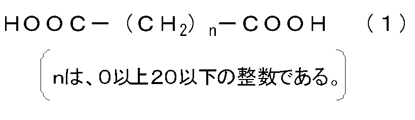
- the method for producing a semiconductor component according to (12), wherein the compound having the flux activity is represented by the following formula (1).
- the semiconductor component manufacturing method and semiconductor component of the present invention will be described.
- the method of manufacturing a semiconductor component according to the present invention includes a step of preparing a semiconductor wafer having a protruding electrode formed on a functional surface, and a circuit board having solder bumps on one side and electrode pads on the other side. And providing a resin layer having flux activity between the semiconductor wafer and the circuit board, and penetrating through the resin layer having flux activity and contacting the bump electrode and the solder bump with the semiconductor wafer A bonding step of bonding the circuit board to obtain a bonded body, a step of applying a solder material to the electrode pads of the bonded body, and a step of cutting the bonded body to obtain a plurality of semiconductor components. It is characterized by that. As described above, a plurality of semiconductor components can be efficiently produced by performing a dicing process or the like after collectively laminating with a circuit board at a semiconductor wafer level.
- FIG. 1 is a cross-sectional view showing a state where protruding electrodes are formed on the functional surface of a semiconductor wafer.
- a semiconductor wafer 1 having a plurality of protruding electrodes 12 formed on the functional surface 11 side of the semiconductor wafer 1 is prepared.
- the protruding electrode 12 include a gold bump, a copper bump or a copper post, a solder bump, and the like.
- a gold bump capable of sharpening the tip is preferable. Thereby, bondability can be improved.
- the pitch (distance between the centers) of such protruding electrodes 12 is currently about 50 to 300 ⁇ m, but is not limited to this, and it is possible to cope with even a narrower pitch (hereinafter, “ “To” represents an upper limit and a lower limit unless otherwise specified).
- a circuit board 2 having a solder bump 21 on one side and an electrode pad 22 on the other side is prepared.
- the circuit board 2 is not particularly limited, and any of a rigid circuit board and a flexible circuit board can be used. However, it is preferable to use a flexible circuit board from the viewpoint of forming vias at a narrow pitch or from an economical viewpoint.
- solder bumps 21 are formed in the vias of the support base material 23.
- a wiring pattern 24 is formed on the support base material 23. Further, one surface of the support base material 23 is covered with a solder resist 25.
- the electrode pads 22 serve as input / output terminals for a mother board, a module substrate, etc., for example, the pitch between the electrode pads 22 is currently often handled as 0.3 to 0.8 mm, but is not limited thereto. Even narrow pitches can be handled.
- the electrode pad 22 is preferably subjected to nickel / gold plating rather than copper stripping from the viewpoint of suppressing metal diffusion and metal compound generation.
- FIG. 7A shows the layout of the functional surface 11 of the semiconductor wafer 1.
- FIG. 7B shows a layout of the joint portion 26 (functional surface) of the circuit board 2.
- the layout of the functional surface 11 and the layout of the joint portion 26 have the same arrangement pattern.
- the arrangement pattern is not particularly limited, but is an array.
- a plurality of protruding electrodes are formed on the functional surface 11.
- a plurality of solder bumps are formed on one side of the joint 26, and a plurality of electrode pads (not shown) are formed on the other side.
- the opening 30 is formed so as to surround the joint portion 26 of the circuit board 2.
- openings 30 are formed on the four sides of the joint portion 26, respectively. That is, four openings 30 are formed substantially parallel to the upper, lower, left and right sides of the joint portion 26.
- two openings 30 are formed substantially parallel to the upper and lower sides of the joint portion 26. The opening 30 penetrates from the front surface to the back surface of the circuit board 2.
- the circuit board 2 is provided with the opening 30 that can exude the resin layer 13 having flux activity when the semiconductor wafer 1 and the circuit board 2 are bonded. Is preferable (FIGS. 7C and 7D).
- the resin layer 13 component having excessive flux activity can be guided to ooze out to the position of the opening 30.
- each opening 30 is formed on a dicing line. That is, the plurality of openings 30 that are substantially parallel to the upper side of the joint portion 26 are formed to be parallel to the upper side direction of the joint portion 26. For this reason, the opening part 30 can be deleted in the case of dicing. That is, the resin layer 13 component having flux activity that has oozed out from the opening 30 can be removed without wiping. Therefore, the number of processes as a whole can be reduced. That is, the productivity of semiconductor components can be improved.
- a plurality of openings 30 may be continuously formed on one side of the joint portion 26. Moreover, as shown in FIG.7 (c), it is preferable that the four opening parts 30 are formed with respect to the one junction part 26. As shown in FIG. The more openings 30 with respect to one joint portion 26, the more efficiently the resin layer 13 component having flux activity can be oozed out. Thereby, the position shift of the protruding electrode 12 and the solder bump 21 can be further reduced.
- the shape of the opening 30 is not particularly limited.
- the shape of the opening 30 viewed from the direction perpendicular to the substrate can be a rectangle.
- strength uniformly is desirable, and the opening area should just be an area into which resin can fully flow.
- the width of the opening 30 in the dicing direction may be the same as the length of the side of the joint 26 or may be smaller than the length of the side. Also.
- the width of the opening 30 in the direction orthogonal to the dicing direction is not particularly limited, but can be, for example, substantially the same as the dicing width.
- the thermal expansion coefficient in the substrate plane direction is not particularly limited, but is preferably 10 [ppm / K] or less, and particularly preferably 4 to 8 [ppm / K].
- the thermal expansion coefficient is within the above range, the batch connectivity is particularly excellent.
- the coefficient of thermal expansion in the plane direction of the board is not particularly limited, but is preferably 15 [ppm / K] or less, and particularly preferably 5 to 12 [ppm / K].
- the thermal expansion coefficient is within the above range, the batch connectivity is particularly excellent.
- the circuit board 2 may have a plurality of (single) circuit boards 51 attached to the support 5. Thereby, the circuit board 2 and the semiconductor wafer 1 can be bonded to a predetermined position, and a plurality of semiconductor components can be obtained by performing a dicing process or the like later.
- a resin layer 13 having flux activity is applied and laminated so as to cover the plurality of protruding electrodes 12 of the semiconductor wafer 1 (FIG. 3). Thereby, it becomes possible to solder-connect the protruding electrode 12 and the solder bump 21 without flux treatment.
- the resin layer 13 having flux activity is disposed on the semiconductor wafer 1 side, and the film of the resin layer 13 having flux activity is disposed.
- the present invention is not limited to this, and the circuit board 2 (the circuit board 2 You may arrange
- the resin composition constituting the resin layer 13 having flux activity contains, for example, a resin capable of crosslinking reaction and a compound having flux activity.
- the resin capable of crosslinking reaction include those classified into so-called thermosetting resins such as epoxy resins, oxetane resins, phenol resins, (meth) acrylate resins, unsaturated polyester resins, diallyl phthalate resins, and maleimide resins.
- thermoplastic resin having a functional group such as a carboxyl group or an epoxy group can also be exemplified as the resin capable of crosslinking reaction of the present invention.
- an epoxy resin excellent in curability and storage stability, heat resistance, moisture resistance, and chemical resistance of a cured product is preferably used.
- epoxy resin either an epoxy resin that is solid at room temperature or an epoxy resin that is liquid at room temperature may be used. Further, an epoxy resin that is solid at room temperature and an epoxy resin that is liquid at room temperature may be used in combination. Thereby, the design freedom of the melting behavior of the resin layer 13 can be further increased.
- the epoxy resin that is solid at room temperature is not particularly limited, and is novolak such as bisphenol A type epoxy resin, bisphenol S type epoxy resin, bisphenol type epoxy resin, phenol novolac type epoxy resin, cresol novolac type epoxy resin, etc.
- the epoxy resin that is solid at room temperature preferably includes a trifunctional epoxy resin and a cresol novolac epoxy resin that are solid at room temperature. Thereby, the moisture resistance reliability of the obtained semiconductor component can be improved.
- the epoxy resin that is liquid at room temperature is not particularly limited, and is bisphenol A type epoxy resin, bisphenol F type epoxy resin, bisphenol A nuclear hydrogenated type epoxy resin, 4-t-butylcatechol type epoxy resin, naphthalene. Type epoxy resin and the like.
- the content of the resin capable of crosslinking reaction is preferably 25% by weight or more and 75% by weight or less, and particularly preferably 45% by weight or more and 70% by weight or less of the entire resin composition. When the content is within the above range, good curability can be obtained, and good melting behavior can be designed.
- the compound having the flux activity is not particularly limited as long as it has an effect of removing the metal oxide film by heating or the like.
- an organic acid such as an active rosin or an organic compound having a carboxy group, an amine, a phenol, an alcohol, an azine, or the like may have a flux activity by itself or promote a flux activity.
- the compound having the flux activity includes a compound having at least one carboxyl group and / or phenolic hydroxyl group in the molecule, which may be liquid or solid.
- examples of the compound having flux activity include divalent carboxylic acids.
- Examples of the compound containing a carboxyl group include aliphatic acid anhydrides, alicyclic acid anhydrides, aromatic acid anhydrides, aliphatic carboxylic acids, and aromatic carboxylic acids.
- Examples of the flux compound having a phenolic hydroxyl group include phenols.
- aliphatic acid anhydride examples include succinic anhydride, polyadipic acid anhydride, polyazeline acid anhydride, polysebacic acid anhydride, and the like.
- Examples of the alicyclic acid anhydride include methyltetrahydrophthalic anhydride, methylhexahydrophthalic anhydride, methylhymic anhydride, hexahydrophthalic anhydride, tetrahydrophthalic anhydride, trialkyltetrahydrophthalic anhydride, methylcyclohexene dicarboxylic acid.
- An acid anhydride etc. are mentioned.
- aromatic acid anhydride examples include phthalic anhydride, trimellitic anhydride, pyromellitic anhydride, benzophenone tetracarboxylic anhydride, ethylene glycol bistrimellitate, glycerol tris trimellitate, and the like.
- Examples of the aliphatic carboxylic acid include compounds represented by the following formula (1).
- the compound represented by the formula (1) is 3 or more in the formula (1), It is preferably 10 or less, particularly preferably 4 or more and 8 or less.
- aliphatic carboxylic acids include formic acid, acetic acid, propionic acid, butyric acid, valeric acid, caproic acid pivalate, caprylic acid, lauric acid, myristic acid, palmitic acid, stearic acid, acrylic acid, methacrylic acid, crotonic acid, Examples include oleic acid, fumaric acid, maleic acid, oxalic acid, malonic acid, and oxalic acid.
- aromatic carboxylic acid examples include benzoic acid, phthalic acid, isophthalic acid, terephthalic acid, hemimellitic acid, trimellitic acid, trimesic acid, merophanic acid, platnic acid, pyromellitic acid, merit acid, triyl acid, and xylyl acid.
- Hemelic acid mesitylene acid, prenylic acid, toluic acid, cinnamic acid, salicylic acid, 2,3-dihydroxybenzoic acid, 2,4-dihydroxybenzoic acid, gentisic acid (2,5-dihydroxybenzoic acid), 2,6 -Dihydroxybenzoic acid, 3,5-dihydroxybenzoic acid, gallic acid (3,4,5-trihydroxybenzoic acid), 1,4-dihydroxy-2-naphthoic acid, 3,5-dihydroxy-2-naphthoic acid Naphthoic acid derivatives such as phenolphthalin; diphenolic acid and the like.
- Examples of the compound having a phenolic hydroxyl group include phenol, o-cresol, 2,6-xylenol, p-cresol, m-cresol, o-ethylphenol, 2,4-xylenol, 2,5 xylenol, m-ethyl.
- the compound which has such flux activity is a hardening
- the reliability can be further improved.
- the curing agent having this flux activity for example, at least two phenolic hydroxyl groups that can be added to a resin capable of crosslinking reaction such as an epoxy resin in one molecule, and a flux action on a metal oxide film, Examples thereof include compounds having at least one carboxyl group directly bonded to an aromatic group in one molecule.
- Benzoic acid derivatives such as acids (3,4,5-trihydroxybenzoic acid); 1,4-dihydroxy-2-naphthoic acid, 3,5-dihydroxy-2-naphthoic acid, 3,7-dihydroxy-2-naphthoic acid Naphthoic acid derivatives such as acids; phenolphthaline; and diphenolic acid.
- These compounds having flux activity may be used alone or in combination of two or more.
- the content of the compound having the flux activity is not particularly limited, but is preferably 1% by weight or more and 30% by weight or less of the entire resin composition, and particularly 5% by weight or more and 25% by weight or less. Is preferred. If the content is less than the lower limit, the effect of flux activity may be insufficient, and if the content exceeds the upper limit, a resin capable of crosslinking reaction and a compound having unreacted flux activity may remain, May cause migration. Further, when the content is within the above range, the oxide film on the surface of the copper foil is reduced, and a good bond having high strength can be obtained.
- the resin composition is not particularly limited, but may contain a curing agent.
- the curing agent include phenols, amines, and thiols.
- an epoxy resin is used as a resin capable of crosslinking reaction, good reactivity with the epoxy resin, low dimensional change upon curing, and appropriate physical properties after curing (for example, heat resistance, moisture resistance, etc.) are obtained.
- phenols are preferably used.
- the phenols are not particularly limited, but are preferably bifunctional or more in view of the physical properties after the adhesive layer 2 is cured.
- Examples include bisphenol A, tetramethylbisphenol A, diallyl bisphenol A, biphenol, bisphenol F, diallyl bisphenol F, trisphenol, tetrakisphenol, phenol novolacs, cresol novolacs, etc., but melt viscosity, reaction with epoxy resin
- phenol novolacs and cresol novolacs can be preferably used.
- the content is not particularly limited, but from the viewpoint of surely curing the crosslinkable resin, it is preferably 5% by weight or more of the total resin composition, 10 weight% or more is preferable. Moreover, if epoxy resin and unreacted phenol novolak remain, it causes migration. Therefore, in order not to remain as a residue, the content is preferably 30% by weight or less, and particularly preferably 25% by weight or less, based on the entire resin composition.
- the content of the phenol novolac resin may be defined by an equivalent ratio with respect to the epoxy resin.
- the equivalent ratio of phenol novolac to epoxy resin is preferably 0.5 or more and 1.2 or less, particularly preferably 0.6 or more and 1.1 or less, and most preferably 0.7 or more and 0.98 or less. Is preferred.
- Examples of other curing agents include imidazole compounds and phosphorus compounds.
- Examples of the imidazole compound include imidazole, 2-methylimidazole, 2-undecylimidazole, 2-heptadecylimidazole, 1,2-dimethylimidazole, 2-ethyl-4-methylimidazole, 2-phenylimidazole, and 2-phenylimidazole.
- imidazole compounds it is preferable to use an imidazole compound having a melting point of 150 ° C. or higher. Thereby, it becomes easy to aim at coexistence with hardening of the resin layer 13, and a flux function. That is, if the melting point of the imidazole compound is too low, the oxide film of the solder bump 21 is removed, and the resin layer 13 is cured before the solder bump 21 and the bump electrode 12 are metal-bonded, resulting in unstable connection. And the case where the preservability of the resin layer 13 falls can be suppressed. Examples of the imidazole compound having a melting point of 150 ° C.
- the content is not particularly limited, but is preferably 0.005% by weight or more and 10% by weight or less of the entire resin composition, particularly 0.01% by weight or more, 5% by weight or less is preferable.
- the function as a curing catalyst of resin which can perform a crosslinking reaction can be exhibited more effectively, and the sclerosis
- the melt viscosity of the resin is not too high at the temperature at which the solder melts, and a good solder joint structure is obtained.
- the preservability of the resin layer 13 can be further improved.
- Examples of the phosphorus compound include triphenylphosphine; a molecular compound of a tetra-substituted phosphonium and a polyfunctional phenol compound; a molecular compound of a tetra-substituted phosphonium, a proton donor, and a trialkoxysilane compound.
- a molecular compound of tetra-substituted phosphonium and a polyfunctional phenol compound, and a tetra-substituted compound which are excellent in rapid curing of the resin layer 13, corrosiveness to an aluminum pad of a semiconductor element, and storage stability of the resin layer 13.
- a molecular compound of phosphonium, a proton donor, and a trialkoxysilane compound is particularly preferable.
- the resin composition is not particularly limited, but may include a film-forming resin different from the resin capable of crosslinking reaction.
- the film-forming resin include phenoxy resin, polyester resin, polyurethane resin, polyimide resin, siloxane-modified polyimide resin, polybutadiene, polypropylene, styrene-butadiene-styrene copolymer, styrene-ethylene-butylene-styrene copolymer, Polyacetal resin, polyvinyl butyral resin, polyvinyl acetal resin, butyl rubber, chloroprene rubber, polyamide resin, acrylonitrile-butadiene copolymer, acrylonitrile-butadiene-acrylic acid copolymer, acrylonitrile-butadiene-styrene copolymer, polyvinyl acetate, nylon Acrylic rubber or the like can be used. These may be used alone or in combination of two or more.
- a phenoxy resin having a number average molecular weight of 5000 to 15000 is preferable.
- the fluidity of the resin layer 13 before curing can be suppressed, and the interlayer thickness can be made uniform.
- the skeleton of the phenoxy resin include, but are not limited to, bisphenol A type, bisphenol F type, and biphenyl skeleton type.
- a phenoxy resin having a saturated water absorption rate of 1% or less is preferable because foaming, peeling, and the like can be suppressed even at high temperatures during bonding and solder mounting.
- a resin having a nitrile group, an epoxy group, a hydroxyl group, or a carboxyl group may be used for the purpose of improving adhesiveness or compatibility with other resins.
- acrylic rubber can be used as the film-forming resin.
- acrylic rubber it is possible to improve film formation stability when the film-like resin layer 13 is produced.
- the elastic modulus of the resin layer 13 can be reduced and the residual stress between the adherend and the resin layer 13 can be reduced, the adhesion to the adherend can be improved.
- the acrylic rubber is preferably a (meth) acrylic acid ester copolymer containing a monomer unit having an epoxy group, a hydroxyl group, a carboxyl group, a nitrile group or the like.
- monomers used in such a (meth) acrylic acid ester copolymer include glycidyl (meth) acrylate having a glycidyl group, (meth) acrylate having a hydroxyl group, (meth) acrylate having a carboxyl group, and a nitrile group. Examples include (meth) acrylonitrile.
- the content of the monomer unit having a carboxyl group in the copolymer is further improved in terms of improving the adhesion to the adherend.
- it is 0.5% by weight or more, preferably 1% by weight or more of the entire (meth) acrylic acid ester copolymer.
- the content of the monomer unit having a carboxyl group is, for example, 10% by weight or less, preferably 5% by weight or less, based on the total (meth) acrylate copolymer, from the viewpoint of further improving the storage stability of the resin layer 13. It is.
- the weight average molecular weight of the (meth) acrylic acid ester copolymer is, for example, 1,000 or more and 1,000,000 or less, and preferably 3,000 or more and 900,000 or less. By setting it as the said range, the film formability of the resin layer 13 can further be improved and the fluidity at the time of adhesion
- the weight average molecular weight of the (meth) acrylic acid ester copolymer can be measured, for example, by gel permeation chromatography (GPC).
- GPC gel permeation chromatography
- Examples of measurement conditions include, for example, high-speed GPC SC- manufactured by Tosoh Corporation.
- TSK-GEL GMHXL-L, temperature 40 ° C., and solvent tetrahydrofuran can be used as the column.
- the glass transition temperature of the (meth) acrylic acid ester copolymer is, for example, 0 ° C. or higher, preferably 5 ° C. or higher, from the viewpoint of further improving workability by suppressing the adhesion of the adhesive film from becoming too strong. Further, the glass transition temperature of the (meth) acrylic acid ester copolymer is, for example, 30 ° C. or less, preferably 20 ° C. or less, from the viewpoint of further improving the adhesiveness at a low temperature.
- the glass transition temperature of the (meth) acrylic acid ester copolymer is increased from ⁇ 65 ° C. at a constant load (10 mN) using, for example, a thermomechanical characteristic analyzer (manufactured by Seiko Instruments Inc., TMA / SS6100). It can be measured from the inflection point when pulled while increasing the temperature at a temperature rate of 5 ° C./min.
- the content of the film-forming resin is not particularly limited, but is preferably 5% by weight or more and 50% by weight or less of the entire resin composition.
- a decrease in film formability is suppressed, and an increase in elastic modulus after the resin layer 13 is cured is suppressed. Can be further improved. Moreover, by setting it as the said range, the increase in the melt viscosity of the resin layer 13 is suppressed.
- an inorganic filler examples include silicates such as talc, fired clay, unfired clay, mica, and glass, titanium oxide, alumina, fused silica (fused spherical silica, fused crushed silica), and powders such as crystalline silica.
- Oxides such as calcium carbonate, magnesium carbonate, hydrotalcite, hydroxides such as aluminum hydroxide, magnesium hydroxide, calcium hydroxide, sulfates such as barium sulfate, calcium sulfate, calcium sulfite, or sulfite Examples thereof include salts, borates such as zinc borate, barium metaborate, aluminum borate, calcium borate, and sodium borate, and nitrides such as aluminum nitride, boron nitride, and silicon nitride. These inorganic fillers may be used alone or in combination. Among these, silica powders such as fused silica and crystalline silica are preferable, and spherical fused silica is particularly preferable.
- an inorganic filler in the resin composition, the heat resistance, moisture resistance, strength and the like after the resin composition is cured can be improved, and the peelability of the resin layer 13 can be improved.
- shape of an inorganic filler is not specifically limited, It is preferable that it is a perfect spherical shape, and can provide the resin composition suitable as the resin layer 13 especially without anisotropy by this.
- the average particle size of the inorganic filler is not particularly limited, but is preferably 0.5 ⁇ m or less, particularly preferably 0.01 to 0.45 ⁇ m, and most preferably 0.01 to 0.3 ⁇ m. If the average particle size is too small, the inorganic filler tends to aggregate, resulting in a decrease in strength. On the other hand, if the average particle size is too large, the transparency of the resin layer 13 is decreased, and the alignment mark on the surface of the semiconductor element is reduced. May be difficult to recognize, and it may be difficult to align the semiconductor element and the substrate.
- the content of the inorganic filler is not particularly limited, but is preferably 10 to 60% by weight, particularly preferably 20 to 50% by weight, based on the entire resin composition. If the content of the inorganic filler is too small, the effect of improving the heat resistance, moisture resistance, strength, etc. may be reduced. It may decrease.
- the resin composition may further contain a silane coupling agent.
- a silane coupling agent By setting it as the structure containing a silane coupling agent, the adhesiveness to the to-be-adhered thing of the resin layer 13 can further be improved.
- the silane coupling agent include an epoxy silane coupling agent and an aromatic-containing aminosilane coupling agent. These may be used alone or in combination of two or more.
- the content of the silane coupling agent is not particularly limited, but is preferably 0.01 to 5% by weight of the entire resin composition.
- the resin composition may contain components other than those described above.
- various additives may be appropriately added in order to improve various properties such as resin compatibility, stability, and workability.
- the semiconductor wafer 1 provided with the resin layer 13 having the flux activity and the circuit board 2 are joined via the resin layer 13 having the flux activity so that the protruding electrodes 12 and the solder bumps 21 are in contact with each other.
- the joined body 3 is obtained (FIG. 4).
- the protruding electrode 12 penetrates through the resin layer 13 having a flux activity provided between the semiconductor wafer 1 and the circuit board 2 and comes into contact with the solder bump 21.
- the protruding electrode 12 contacts the solder bump 21 in a state where the protruding electrode 12 and the solder bump 21 are covered with the resin layer 13 having flux activity.
- the bonding conditions are not particularly limited, but after temporarily pressing (connecting) the protruding electrodes 12 and the solder bumps 21 at 25 to 175 ° C. and 0.5 to 5 kgf per unit, the solder portions are bonded.
- 0.1 to 15 kgf per unit is preferable at 200 to 300 ° C. for 1 to 60 seconds.
- 200 to 230 ° C. ⁇ 5 to 180 seconds is preferable.
- the bonding temperature depends on the melting point of the solder type of the solder bump, and the load depends on the number of terminals to be bonded.
- the bump electrode 12 and the solder bump 21 are joined via the resin layer 13 having flux activity, the surface of the solder bump 21 is suppressed from being oxidized (while the surface oxide film is removed). Solder can be connected.
- the resin constituting the resin layer 13 having flux activity by further heating the joined body 3.
- the heating conditions at this time are not particularly limited, but are preferably 120 to 200 ° C. ⁇ 30 to 180 minutes.
- the resin layer 13 having flux activity is cured, so that the gap between the protruding electrodes 12 and the solder bumps 21 is increased. Sealing can improve the connection reliability.
- the resin layer 13 having the flux activity is cured after obtaining the joined body 13.
- the present invention is not limited thereto, and the joined body 13 is cured after the resin layer 13 having the flux activity is cured. You can get it.
- solder material is applied to the electrode pads 22 of the joined body 3.
- solder material for example, a solder ball 4 as shown in FIG. 5 is preferable. This facilitates secondary mounting on another board or the like.
- a method for applying the solder ball 4 include a plating method, a paste printing method, and a ball mounting method.
- the joined body 3 having the solder balls 4 is diced to obtain a plurality of semiconductor components 31.
- dicing is performed by applying a dicing sheet to the surface of the bonded body 3 opposite to the side where the solder balls 4 are applied.
- a dicing sheet to be used what is marketed can be used as it is.
- Example 1 Manufacture of semiconductor wafer having protruding electrodes
- Gold stud bumps were formed on a 70 ⁇ m pitch AL pad on a semiconductor wafer (6 inch diameter, 250 ⁇ m thickness) with a bump bonder by a gold wire board bonding method.
- the gold stud bumps had a bump diameter of 30 to 35 ⁇ m, a bump pedestal of 15 to 20 ⁇ m, and a bump height of 40 to 45 ⁇ m, and the tip remained sharp without any processing such as leveling.
- solder resist is printed and applied, and pre-curing, exposing, developing, and post-curing, so that only the lands that are external connection terminals are exposed, and solder bumps are applied by plating the lands with nickel / gold.
- the flexible circuit board which has this was produced.
- the outer shape processing including the opening was performed with a mold.
- a sheet of a resin layer having flux activity was attached to the functional surface side of the semiconductor wafer described above with a vacuum film laminator ("MVLP-500 / 600-2A", manufactured by Meiki Seisakusho).
- the processing conditions for attaching the sheet of the resin layer having flux activity with a vacuum film laminator were 120 ° C., 0.8 MPa, and 30 seconds.
- seat of the resin layer which has the flux activity affixed on the wafer for semiconductors was 30 micrometers.
- the solder bumps and the gold stud bumps were aligned with each other, and preliminarily thermocompression bonded with a press device (VH1-1758).
- Temporary thermocompression bonding conditions were 150 ° C. and 1.0 MPa.
- metal stud bumps on the wafer and molten solder bumps on the flexible circuit board were formed into metal.
- an electrically connected joined body was obtained.
- Example 2 The circuit board was the same as the example except that the following was used.
- a support base material for a flexible circuit board having solder bumps a substrate to which polyimide having a linear expansion coefficient of 2.5 ppm / K (manufactured by Toyobo) was applied was used.
- Example 3 The circuit board was the same as Example 1 except that a circuit board 51 having a plurality of circuit boards 51 attached to the support 5 as shown in FIG. 6 was used. In this case, one having no opening was used.
- Example 4 The circuit board was the same as Example 1 except that the following was used.
- a copper foil-laminated copper-clad laminate (ELC-4785GS manufactured by Sumitomo Bakelite Co., Ltd., linear expansion coefficient 9 ppm / K) having a thickness of 12 ⁇ m and 30 ⁇ m was applied as a circuit board.
- Example 5 The resin layer having flux activity was the same as that of Example 1 except that the following was used.
- An epoxy resin (NC6000 (epoxy equivalent 200 g / eq, manufactured by Nippon Kayaku Co., Ltd.)) 47.4% by weight as a resin capable of crosslinking reaction, and an acrylate copolymer (butyl acrylate-ethyl acrylate-acrylonitrile) as a film-forming resin -Acrylic acid-hydroxyethyl acrylate copolymer, manufactured by Nagase ChemteX Corporation, SG-708-6, weight average molecular weight: 500,000) 14.6% by weight and acrylic resin (acrylic acid-styrene copolymer, weight) Average molecular weight: 5,500, UC-3900, manufactured by Toagosei Co., Ltd.) 14.6% by weight, solid phenol resin (PR-53647, hydroxyl group equivalent 104 g / OH group, manufactured by Sumitomo Bakelite
- Sebacic acid 6.4% by weight as a flux compound propyltrimethoxysilane (KBM303, manufactured by Shin-Etsu Chemical Co., Ltd.) as a coupling agent 0.4% by weight acrylic polymer (BYK-361N, manufactured by BYK Japan Japan) as a leveling agent 0.1% by weight was dissolved in methyl ethyl ketone to obtain a resin varnish having a resin solid content of 40%, and the obtained varnish was applied to a polyester sheet, appropriately set to a temperature at which the solvent evaporates, and the varnish was dried. Thus, a resin layer sheet having flux activity was obtained.
- KBM303 propyltrimethoxysilane
- acrylic polymer BYK-361N, manufactured by BYK Japan Japan
- Comparative Example 1 As a comparative example, a flip chip CSP (chip size package) was manufactured. A photosensitive polyimide (CRC-8300, manufactured by Sumitomo Bakelite Co., Ltd.) is applied onto a semiconductor wafer (size: 6 inches, thickness 350 ⁇ m) with a spin coater, and the AL pad is opened by exposing, developing and curing the AL pad. Then, the electroless plating of nickel and then the electroless plating of gold were applied to the opening, solder balls were mounted, and dicing into chip sizes.
- CRC-8300 manufactured by Sumitomo Bakelite Co., Ltd.
- a chip having the solder ball mounted thereon and the terminal of the substrate were joined to a rigid substrate (manufactured by Arm Electronics Co., Ltd.) having a terminal at the same position as the solder ball mounted.
- a pre-solder was formed on the terminal on the rigid substrate surface by printing, and the solder oxide film of the upper and lower solders was removed by flux before joining. After the joining, the flux was washed, and a capillary underfill (manufactured by Sumitomo Bakelite Co., Ltd., CRP-4152D) was poured into the gap at the joining portion to be cured.
- Area terminals for mounting on the mounting board are formed on the back side of the rigid board, and the front side terminal and the back side terminal are connected by a copper circuit.
- a flip chip type CSP was obtained by mounting solder balls on the area terminals.
- Comparative Example 2 As a comparative example, a rewiring type wafer level CSP was manufactured. Photosensitive polyimide (CRC-8300, manufactured by Sumitomo Bakelite Co., Ltd.) is coated on a semiconductor wafer (size: 6 inches, thickness 450 ⁇ m) with a spin coater, and the AL pad is exposed, developed and cured to open the AL pad. A titanium film having a thickness of 500 angstroms is formed by titanium sputtering, a copper film having a thickness of 3,000 angstroms is stacked by copper sputtering, a resist is applied, and a chip terminal is connected to an external connection area terminal of the mounting substrate.
- Photosensitive polyimide CRC-8300, manufactured by Sumitomo Bakelite Co., Ltd.
- a titanium film having a thickness of 500 angstroms is formed by titanium sputtering
- a copper film having a thickness of 3,000 angstroms is stacked by copper sputtering
- a resist is applied
- connection reliability was evaluated based on whether or not the obtained semiconductor component could be conducted after a temperature cycle test. Specifically, the connection resistance between the semiconductor element and the substrate was measured with a digital multi-digital multimeter. The measurement was performed both after manufacturing the semiconductor component and after 1,000 cycles of a temperature cycle of -65 ° C for 1 hour and 150 ° C for 1 hour. Each code is as follows. A: Conductivity was obtained with 20/20 semiconductor parts. ⁇ : Conductivity was obtained with 18 to 19/20 semiconductor parts. ⁇ : Conductivity was obtained with 16 to 17/20 semiconductor parts. X: Conductivity was obtained with 16 or less / 20 semiconductor components.
- Reflow crack resistance is obtained by subjecting the obtained semiconductor component to moisture absorption treatment in a constant temperature and humidity chamber at 85 ° C. and 85% relative humidity for 168 hours, and then quickly using a reflow apparatus (Max 260 degrees). 10 sec), and the presence or absence of internal peeling was confirmed with an ultrasonic flaw detector (SAT). The processing was in accordance with JEDEC standards. Each code is as follows. The n number was 20. ⁇ : No internal peeling after treatment ⁇ : Internal peeling after treatment
- Examples 1 to 5 were confirmed to be excellent in productivity.
- the semiconductor components obtained in Examples 1 to 5 were excellent in connection reliability and reflow crack resistance.
Landscapes
- Chemical & Material Sciences (AREA)
- Organic Chemistry (AREA)
- Wire Bonding (AREA)
- Structures Or Materials For Encapsulating Or Coating Semiconductor Devices Or Solid State Devices (AREA)
- Encapsulation Of And Coatings For Semiconductor Or Solid State Devices (AREA)
Abstract
Description
(1)機能面に突起電極が形成された半導体ウエハと、一方面の側に半田バンプを有し他方面の側に電極パッドを有する回路基板と、を用意する工程と、
前記半導体ウエハと前記回路基板と間にフラックス活性を有する樹脂層を設けるとともに、前記フラックス活性を有する樹脂層を突き抜けて前記突起電極と前記半田バンプとが当接するように、前記半導体ウエハと前記回路基板とを接合して接合体を得る接合工程と、
前記接合体の前記電極パッドに半田材を付与する工程と、
前記接合体を切断して複数の半導体部品を得る工程と、を含む、半導体部品の製造方法。
(2)前記回路基板には、前記半導体ウエハと前記回路基板とを接合した際に、前記フラックス活性を有する樹脂層が染み出す開口部が形成されている、(1)に記載の半導体部品の製造方法。
(3)前記フラックス活性を有する樹脂層は、フィルムであり、
前記接合工程おいて、前記フィルムを前記半導体ウエハの前記機能面に貼り付けた状態で、前記半導体ウエハと前記回路基板とを接合する、(1)または(2)に記載の半導体部品の製造方法。
(4)前記フラックス活性を有する樹脂層は、フィルムであり、
前記接合工程おいて、前記フィルムを前記回路基板の前記半田バンプを有する面に貼り付けた状態で、前記半導体ウエハと前記回路基板とを接合する、(1)または(2)に記載の半導体部品の製造方法。
(5)前記回路基板が、フレキシブル回路基板である、(1)または(2)に記載の半導体部品の製造方法。
(6)前記回路基板が、リジッド回路基板である、(1)または(2)に記載の半導体部品の製造方法。
(7)前記フレキシブル回路基板の基板平面方向の熱膨張係数が、10[ppm/K]以下である、(5)に記載の半導体部品の製造方法。
(8)前記フレキシブル回路基板の基板平面方向の熱膨張係数が、4[ppm/K]以上である、(5)に記載の半導体部品の製造方法。
(9)前記リジッド回路基板の基板平面方向の熱膨張係数が、15[ppm/K]以下である、(6)に記載の半導体部品の製造方法。
(10)前記リジッド回路基板の基板平面方向の熱膨張係数が、5[ppm/K]以上である、(6)に記載の半導体部品の製造方法。
(11)前記回路基板は、支持体に複数の回路基板が貼着されてなるものである、(1)または(2)に記載の半導体部品の製造方法。
(12)前記フラックス活性を有する樹脂層は、架橋反応可能な樹脂と、フラックス活性を有する化合物とを含む樹脂組成物で構成されているものである、(1)または(2)に記載の半導体部品の製造方法。
(13)前記フラックス活性を有する化合物は、前記架橋反応可能な樹脂の硬化剤として作用するものである、(12)に記載の半導体部品の製造方法。
(14)前記フラックス活性を有する化合物は、分子中にカルボキシル基またはフェノール性水酸基を、少なくとも1つ以上有する、(12)に記載の半導体部品の製造方法。
(15)前記フラックス活性を有する化合物は、下記式(1)で記載されるものである、(12)に記載の半導体部品の製造方法。

(16)前記半田材が付与された前記電極パッドに、さらにフラックス活性を有する樹脂層を配置するものである、(1)または(2)に記載の半導体部品の製造方法。
(17)(1)または(2)に記載の半導体部品の製造方法で得られた半導体部品。
本発明の半導体部品の製造方法は、機能面に突起電極が形成された半導体ウエハと、一方面の側に半田バンプを有し他方面の側に電極パッドを有する回路基板と、を用意する工程と、上記半導体ウエハと上記回路基板と間にフラックス活性を有する樹脂層を設けるとともに、上記フラックス活性を有する樹脂層を突き抜けて上記突起電極と上記半田バンプとが当接するように、上記半導体ウエハと上記回路基板とを接合して接合体を得る接合工程と、上記接合体の前記電極パッドに半田材を付与する工程と、上記接合体を切断して複数の半導体部品を得る工程と、を含むことを特徴とする。
このように、半導体用ウエハレベルで回路基板と一括積層した後、ダイシング処理等することにより複数の半導体部品を効率良く生産することができるものである。
図1は、半導体ウエハの機能面に突起電極が形成されている状態を示す断面図である。
図1に示すように、半導体用ウエハ1の機能面11側に、複数の突起電極12が形成されている半導体用ウエハ1を用意する。
突起電極12は、例えば金バンプ、バンプの表面にニッケル・金メッキし、更に半田メッキを施した銅バンプもしくは銅ポスト、半田バンプ等を挙げることができる。これらの中でも先端を鋭くすることができる金バンプが好ましい。これにより、接合性を向上することができる。
このような突起電極12同士のピッチ(中心間距離)は、50~300μm程度が現在多く扱われているが、これに限定されず、さらに狭いピッチでも対応することが可能である(以下、「~」は、特に明示しない限り、上限値と下限値を含むことを表す)。
回路基板2としては、特に限定されず、リジッド回路基板、フレキシブル回路基板のいずれを用いることができるが、狭ピッチでのビア形成や経済的な観点でフレキシブル回路基板を用いることが好ましい。
回路基板2の一例としては、図2に示すように、支持基材23のビア内に半田バンプ21が形成されている。この支持基材23上に配線パターン24が形成されている。また、支持基材23の一方面がソルダーレジスト25で覆われている。
電極パッド22は、マザーボードやモジュール基板等への入出力端子となるため、例えば電極パッド22同士のピッチは、0.3~0.8mmが現在多く扱われているが、これに限定されず、さらに狭いピッチでも対応することが可能である。
尚、電極パッド22は銅剥き出しよりも、ニッケル/金メッキを施した方が、金属拡散・金属化合物生成を抑えられる観点から望ましい。
図7(a)は、半導体ウエハ1の機能面11のレイアウトを示す。図7(b)は、回路基板2の接合部26(機能面)のレイアウトを示す。機能面11のレイアウトと接合部26のレイアウトとは、同じ配置パターンとする。配置パターンとしては、特に限定されないが、アレイ状とする。機能面11には、複数の突起電極(図示せず)が形成されている。一方、接合部26の一方面の側に複数の半田バンプ(図示せず)が形成され、他方の面側に複数の電極パッド(図示せず)が形成されている。
このとき、図7(c)(d)に示すように、回路基板2の接合部26を囲むように開口部30が形成されている。図7(c)では、接合部26の4辺に、それぞれ開口部30が形成されている。つまり、接合部26の上下左右の辺に対して略平行に4つの開口部30が形成されている。また、図7(d)では、接合部26の上下の辺に対して略平行に2つの開口部30が形成されている。この開口部30は、回路基板2の表面から裏面を貫通する。
なお、本実施形態では、フラックス活性を有する樹脂層13を半導体用ウエハ1側に、フラックス活性を有する樹脂層13のフィルムを配置したが、これに限定されず、回路基板2(回路基板2の半田バンプ21側の面)にフラックス活性を有する樹脂層13のフィルムを配置しても良い。すなわち、半導体用ウエハ1と回路基板2の間のいずれか一方の面に、フラックス活性を有する樹脂層13のフィルムが貼り付けられた状態で配置されていればよい。
フラックス活性を有する樹脂層13を構成する樹脂組成物は、例えば架橋反応可能な樹脂と、フラックス活性を有する化合物とを含んでいる。
前記架橋反応可能な樹脂としては、例えばエポキシ樹脂、オキセタン樹脂、フェノール樹脂、(メタ)アクリレート樹脂、不飽和ポリエステル樹脂、ジアリルフタレート樹脂、マレイミド樹脂等のいわゆる熱硬化性樹脂に分類されるものに加え、カルボキシル基、エポキシ基等の官能基を有する熱可塑性樹脂等も本発明の架橋反応可能な樹脂として挙げることができる。これらの中でも、硬化性と保存性、硬化物の耐熱性、耐湿性、耐薬品性に優れるエポキシ樹脂が好適に用いられる。
このフラックス活性を有する化合物として、より具体的には分子中にカルボキシル基および/またはフェノール性水酸基を少なくとも1つ以上有する化合物が挙げられ、これは液状であっても固体であっても構わない。たとえば、フラックス活性を有する化合物としては、たとえば、2価のカルボン酸が挙げられる。
他の脂肪族カルボン酸としては、蟻酸、酢酸、プロピオン酸、酪酸、吉草酸、ピバル酸カプロン酸、カプリル酸、ラウリン酸、ミリスチン酸、パルミチン酸、ステアリン酸、アクリル酸、メタクリル酸、クロトン酸、オレイン酸、フマル酸、マレイン酸、シュウ酸、マロン酸、琥珀酸等が挙げられる。
このフラックス活性を有する硬化剤としては、例えば1分子中にエポキシ樹脂等の架橋反応可能な樹脂に付加することができる少なくとも2個のフェノール性水酸基と、金属酸化膜に対してフラックス作用を示す、芳香族に直接結合したカルボキシル基を一分子中に少なくとも1個有する化合物が挙げられる。具体的には、2,3-ジヒドロキシ安息香酸、2,4-ジヒドロキシ安息香酸、ゲンチジン酸(2,5-ジヒドロキシ安息香酸)、2,6-ジヒドロキシ安息香酸、3,4-ジヒドロキシ安息香酸、没食子酸(3,4,5-トリヒドロキシ安息香酸)等の安息香酸誘導体;1,4-ジヒドロキシ-2-ナフトエ酸、3,5-ジヒドロキシ-2-ナフトエ酸、3,7-ジヒドロキシ-2-ナフトエ酸等のナフトエ酸誘導体;フェノールフタリン;およびジフェノール酸等が挙げられる。
これらのフラックス活性を有する化合物は、単独で用いても、2種以上を組み合わせて用いてもよい。
前記硬化剤としては、例えばフェノール類、アミン類、チオール類が挙げられる。架橋反応可能な樹脂としてエポキシ樹脂が用いられる場合、このエポキシ樹脂との良好な反応性、硬化時の低寸法変化および硬化後の適切な物性(例えば、耐熱性、耐湿性等)が得られるという点で、フェノール類が好適に用いられる。
前記イミダゾール化合物としては、例えばイミダゾール、2-メチルイミダゾール、2-ウンデシルイミダゾール、2-ヘプタデシルイミダゾール、1,2-ジメチルイミダゾール、2-エチルー4-メチルイミダゾール、2-フェニルイミダゾール、2-フェニルー-フェニル-4-メチルイミダゾール、1-ベンジル-2-フェニルイミダゾール、1-ベンジル-2-メチルイミダゾール、1-シアノエチル-2-メチルイミダゾール、1-シアノエチル-2-エチル-4-メチルイミダゾール、1-シアノエチル-2-ウンデシルイミダゾール、1-シアノエチル-2-フェニルイミダゾール、1-シアノエチル-2-ウンデシルイミダゾリウムトリメリテイト、1-シアノエチル-2-フェニルイミダゾリウムトリメリテイト、2,4-ジアミノ-6-[2´-メチルイミダゾリル(1´)]-エチル-sトリアジン、2,4-ジアミノ-6-[2´-ウンデシルイミダゾリル(1´)]-エチル-sトリアジン、2,4-ジアミノ-6-[2´-エチル-4-メチルイミダゾリル(1´)]-エチル-sトリアジン、2,4-ジアミノ-6-[2´-メチルイミダゾリル(1´)]-エチル-sトリアジンイソシアヌル酸付加物、2-フェニルイミダゾールイソシアヌル酸付加物、2-メチルイミダゾールイソシアヌル酸付加物、2-フェニルー-フェニル-4,5-ジヒドロキシジメチルイミダゾール、2-フェニル-4-メチル-5-ヒドロキシメチルイミダゾール等が挙げられる。
融点が150℃以上のイミダゾール化合物としては、例えば2-フェニルヒドロキシイミダゾール、2-フェニル-4-メチルヒドロキシイミダゾール、2-フェニル-4-メチルイミダゾール等が挙げられる。なお、イミダゾール化合物の融点の上限に特に制限はなく、例えば樹脂層13の接着温度に応じて適宜設定することができる。
前記フィルム形成性樹脂としては、例えばフェノキシ樹脂、ポリエステル樹脂、ポリウレタン樹脂、ポリイミド樹脂、シロキサン変性ポリイミド樹脂、ポリブタジエン、ポリプロピレン、スチレン-ブタジエン-スチレン共重合体、スチレン-エチレン-ブチレン-スチレン共重合体、ポリアセタール樹脂、ポリビニルブチラール樹脂、ポリビニルアセタール樹脂、ブチルゴム、クロロプレンゴム、ポリアミド樹脂、アクリロニトリル-ブタジエン共重合体、アクリロニトリル-ブタジエン-アクリル酸共重合体、アクリロニトリル-ブタジエン-スチレン共重合体、ポリ酢酸ビニル、ナイロン、アクリルゴム等を用いることができる。これらは、単独で用いても、2種以上を組み合わせて用いてもよい。
フィルム形成性樹脂として、アクリルゴムが用いられる場合、フィルム状の樹脂層13を作製する際の成膜安定性を向上させることができる。また、樹脂層13の弾性率を低下させ、被接着物と樹脂層13間の残留応力を低減することができるため、被接着物に対する密着性を向上させることができる。
接合する条件としては、特に限定されないが、25~175℃、1ユニット当たり0.5~5kgfで突起電極12と半田バンプ21の位置を合わせて仮圧着(接続)をした後、半田部の接合(本接続)を得るために200~300℃×1~60秒間、1ユニット当たり0.1~15kgfが好ましい。特に200~230℃×5~180秒間が好ましい。接合温度は半田バンプの半田種の融点に依存し、荷重は接合する端子数に依存する。
ここで、フラックス活性を有する樹脂層13を介して、突起電極12と半田バンプ21とを接合するので、半田バンプ21の表面が酸化されるのを抑制しながら(表面酸化膜を除去しながら)半田を接続することができるようになる。
この際の加熱条件は、特に限定されないが、120~200℃×30~180分間が好ましく、これにより、フラックス活性を有する樹脂層13が硬化することにより、突起電極12と半田バンプ21の間を封止し、接続信頼性を向上することができる。
なお、本実施形態では、接合体13を得た後、フラックス活性を有する樹脂層13を硬化させたが、これに限定されず、フラックス活性を有する樹脂層13を硬化させた後に接合体13を得る方法でも良い。
半田材としては、例えば図5に示すような半田ボール4が好ましい。これにより、他の基板等への2次実装が容易となる。
半田ボール4を付与する方法としては、例えばメッキ法、ペースト印刷法、ボール搭載法が挙げられる。
なお、ダイシングする前に、接合体3の半田ボール4が付与されている側の面にフラックス活性を有する樹脂層を配置しておくことが好ましい。これにより、2次実装での半田接続が容易となると共に、フラックス処理を省略することができ、生産性や温度サイクル性、落下試験等の2次実装後の信頼性を向上することができる。
ここで、使用するダイシングシートとしては、市販されているものをそのまま用いることができる。
1.突起電極を有する半導体用ウエハの製造
金線ボードボンディング法により、半導体用ウエハ(6inch径、250μm厚さ)上の70μmピッチのALパッドに、バンプボンダーで金スタッドバンプを形成した。金スタッドバンプの形状は、バンプ径30~35μm、バンプ台座が15~20μm、バンプ高さ40~45μmであり、先端はレベリング等の処理を実施しないで鋭角な状態を残した。
銅箔の厚さが12μm、支持基材としてポリイミド(宇部日東社製 BE2508DFF、線膨張係数11ppm/K、厚さ25μm)で構成される銅張板に、レーザー加工により30μm径のビアを形成し、デスミア処理後、半田(Sn-Ag)メッキを施し、ビア内に半田バンプを形成した。
バンプ面を保護した後、銅側にレジストを貼り付け、露光、現像、エッチング、レジスト剥離することで配線パターンを形成した。その後、ソルダーレジストを印刷・塗布し、プレキュア、露光、現像、ポストキュアすることで、外部接続端子であるランドのみが露出した構造になり、ランド部にニッケル/金のメッキを施すことで半田バンプを有するフレキシブル回路基板を作製した。最後に開口部含む外形加工を金型にて実施した。
架橋反応可能な樹脂としてエポキシ樹脂(NC6000、エポキシ当量200g/eq、日本化薬社製)47.0重量%、フィルム形成性樹脂としてアクリル酸エステル共重合体(アクリル酸ブチル-アクリル酸エチル-アクリロニトリル-アクリル酸-アクリル酸ヒドロキシエチル共重合体、ナガセケムテックス社製、SG-708-6、重量平均分子量:500,000)14.6重量%とアクリル樹脂(アクリル酸-スチレン共重合体、重量平均分子量:5,500、UC-3900、東亜合成社製)14.6重量%、硬化剤として固形フェノール樹脂(PR-53647、水酸基当量104g/OH基、住友ベークライト社製)10.3重量%、硬化促進剤としてイミダゾール化合物(2P4MHZ、四国化成工業社製)0.1重量%、フラックス化合物としてフェノールフタリン12.9重量%、カップリング剤としてプロピルトリメトキシシラン(KBM303、信越化学工業社製)0.4量%、レベリング剤としてアクリルポリマー(BYK-361N、ビックケミージャパン社製)0.1重量%をメチルエチルケトンに溶解して樹脂固形分40%の樹脂ワニスを得た。
得られたワニスをポリエステルシート状に塗布し、上記溶剤が揮発する温度に適宜設定し、ワニスを乾燥させることにより、フラックス活性を有する樹脂層のシートを得た。
上述の半導体用ウエハの機能面側に、真空フィルムラミネータ(「MVLP-500/600-2A」、名機製作所製)でフラックス活性を有する樹脂層のシートを貼り付けた。真空フィルムラミネータによりフラックス活性を有する樹脂層のシートを貼り付ける際の処理条件は、120℃、0.8MPa、30秒間とした。半導体用ウエハ上に貼り付けたフラックス活性を有する樹脂層のシートの厚さは30μmであった。
次に、突起電極を有する半導体用ウエハと、半田バンプを有するフレキシブル回路基板の接合については、半田バンプと金スタッドバンプの上下位置を合わせ、プレス装置(VH1-1758)で、仮熱圧着した。仮熱圧着条件は150℃、1.0MPaとした。更に圧力を徐々に開放しながら(0.1MPa以下)、250℃まで加熱することにより、ウエハ上の金スタッドバンプと溶融したフレキシブル回路基板の半田バンプが金属形成した。更に180℃、120分間追加熱することにより、電気的にも接続された接合体(フレキシブル回路基板付きウエハ)が得られた。
得られた半導体用ウエハに半田ボールを搭載し、市販ダイシングシートのカバーフィルムを剥離して、接着フィルム面を6インチ、250μmウエハ厚の裏面に貼り付け、接合体を、ダイシングソー(DISCO製)を用いて、スピンドル回転数30,000rpm、切断速度50mm/secでチップサイズにダイシング(切断)して、複数の半導体部品を得た。
回路基板として、以下のものを用いた以外は、実施例と同様にした。
半田バンプを有するフレキシブル回路基板の支持基材として線膨張係数2.5ppm/Kのポリイミド(東洋紡製)を適用したものを用いた。
回路基板として、図6に示すような支持体5に複数の回路基板51が貼着されてなるものを用いた以外は、実施例1と同様にした。なお、この場合は開口部を有していないものを用いた。
回路基板として、以下のものを用いた以外は、実施例1と同様にした。
回路基板として銅箔の厚さ12μm、30μm厚さガラスクロス入銅張積層板(住友ベークライト社製 ELC-4785GS、線膨張係数9ppm/K)を適用した。
フラックス活性を有する樹脂層として、以下のものを用いた以外は、実施例1と同様にした。
架橋反応可能な樹脂としてエポキシ樹脂(NC6000(エポキシ当量200g/eq、日本化薬社製)47.4重量%、フィルム形成性樹脂としてアクリル酸エステル共重合体(アクリル酸ブチル-アクリル酸エチル-アクリロニトリル-アクリル酸-アクリル酸ヒドロキシエチル共重合体、ナガセケムテックス社製、SG-708-6、重量平均分子量:500,000)14.6重量%とアクリル樹脂(アクリル酸-スチレン共重合体、重量平均分子量:5,500、UC-3900、東亜合成社製)14.6重量%、硬化剤として固形フェノール樹脂(PR-53647、水酸基当量104g/OH基、住友ベークライト社製)16.4重量%、硬化促進剤としてイミダゾール化合物(2P4MHZ、四国化成工業社製)0.1重量%、フラックス化合物としてセバシン酸6.4重量%、カップリング剤としてプロピルトリメトキシシラン(KBM303、信越化学工業社製)0.4量%レベリング剤としてアクリルポリマー(BYK-361N、ビックケミージャパン社製)0.1重量%をメチルエチルケトンに溶解して樹脂固形分40%の樹脂ワニスを得た。得られたワニスをポリエステルシート状に塗布し、上記溶剤が揮発する温度に適宜設定し、ワニスを乾燥させることにより、フラックス活性を有する樹脂層のシートを得た。
比較例としてフリップチップCSP(チップサイズパッケージ)を作製した。
半導体用ウエハ(サイズ:6インチ、厚さ350μm)上に感光性ポリイミド(住友ベークライト社製 CRC-8300)をスピンコータにより、塗布し、ALパッドを露光・現像・硬化することでALパッドが開口させ、開口部にニッケルの無電解メッキ、ついで金の無電解メッキを施し、半田ボールを搭載し、チップサイズにダイシングした。
次に、半田ボールが搭載されたのと同じ位置に端子を有するリジッド基板(アーム電子社製)にフリップチップボンダーを用いて、前述した半田ボールが搭載されたチップと基板の端子を接合した。尚、リジット基板表側の端子にはプレソルダーを印刷により形成し、接合前に上下半田の半田酸化膜をフラックスにより除去した。
接合後、フラックスを洗浄し、接合部のギャップへキャピラリーアンダーフィル(住友ベークライト社製、CRP-4152D)を流し込み、硬化した。リジット基板裏側には実装基板へ実装するためのエリア端子が形成されており、表側端子と裏側の端子は銅の回路で接続されている。エリア端子に半田ボールを搭載することでフリップチップタイプのCSPを得た。
比較例として再配線タイプのウエハレベルCSPを作製した。
半導体用ウエハ(サイズ:6インチ、厚さ450μm)上に感光性ポリイミド(住友ベークライト社製 CRC-8300)をスピンコータにより、塗布し、ALパッドを露光・現像・硬化することでALパッドが開口させ、チタンスパッタリングにより厚さが500オングストロームのチタン膜を形成し、更に銅スパッタリングにより、3,000オングストロームの銅膜を重ねた後、レジストを塗布し、チップの端子から、実装基板の外部接続エリア端子に引き回すための回路パターンを露光、現像処理した後、回路パターン部分のみ銅メッキを施した。その後、レジストを剥離し、銅膜及びチタン膜をエッチング処理することでウエハ上に銅の回路パターンを形成した。更に絶縁層として、感光性ポリイミド(住友ベークライト社製 CRC-3900)をその上再度塗布し、ランドパターンを露光・現像・硬化することで外部端子を形成し、ランド部分をニッケルメッキ、次いで金メッキした後、ランド部分に半田ボールを搭載し、チップサイズにダイシングすることで半導体部品を得た。
比較例1の生産工数を基準(100)として、他の実施例および比較例の生産性を比較した。各符号は、以下の通りである。
◎:比較例1の生産工数を基準(100)として、生産工数が40以上、60未満であった。
○:比較例1の生産工数を基準(100)として、生産工数が60以上、80未満であった。
△:比較例1の生産工数を基準(100)として、生産工数が80以上、100未満であった。
×:比較例1の生産工数を基準(100)として、生産工数が100以上であった。
接続信頼性は、得られた半導体部品を温度サイクル試験後に導通がとれるかどうかで評価した。
具体的には、半導体素子、基板間の接続抵抗を、デジタルマルデジタルマルチメータにより測定した。測定は半導体部品を作製後と、-65℃で1時間および150℃で1時間の温度サイクル1,000サイクル後の両方を測定した。各符号は、以下の通りである。
◎:20/20個の半導体部品で導通が取れた。
○:18~19/20個の半導体部品で導通が取れた。
△:16~17/20の半導体部品で導通が取れた。
×:16以下/20の半導体部品で導通が取れた。
耐リフロークラック性は、得られた半導体部品を85℃、相対湿度85%の恒温恒湿槽にて168時間、吸湿処理した後、速やかにリフロー装置を用いてリフロー処理(Max260度10sec)を行い、超音波探傷機(SAT)にて内部剥離の有無を確認した。尚、処理についてはJEDECの標準に準じた。各符号は、以下の通りである。n数は20とした。
◎:処理後、内部剥離が発生なし
×:処理後、内部剥離発生あり
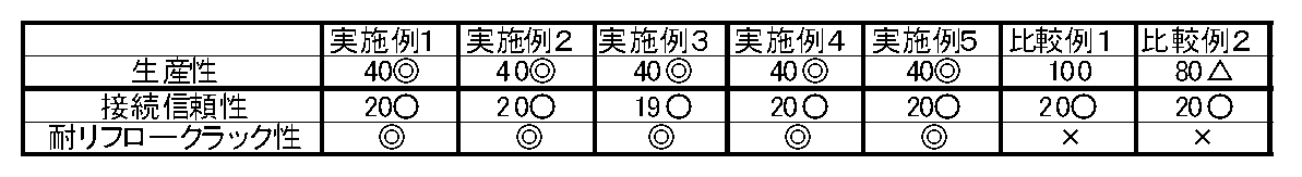
また、実施例1~5で得られた半導体部品は、接続信頼性および耐リフロークラック性にも優れていた。
Claims (17)
- 機能面に突起電極が形成された半導体ウエハと、一方面の側に半田バンプを有し他方面の側に電極パッドを有する回路基板と、を用意する工程と、
前記半導体ウエハと前記回路基板と間にフラックス活性を有する樹脂層を設けるとともに、前記フラックス活性を有する樹脂層を突き抜けて前記突起電極と前記半田バンプとが当接するように、前記半導体ウエハと前記回路基板とを接合して接合体を得る接合工程と、
前記接合体の前記電極パッドに半田材を付与する工程と、
前記接合体を切断して複数の半導体部品を得る工程と、を含む、半導体部品の製造方法。 - 前記回路基板には、前記半導体ウエハと前記回路基板とを接合した際に、前記フラックス活性を有する樹脂層が染み出す開口部が形成されている、請求項1に記載の半導体部品の製造方法。
- 前記フラックス活性を有する樹脂層は、フィルムであり、
前記接合工程おいて、前記フィルムを前記半導体ウエハの前記機能面に貼り付けた状態で、前記半導体ウエハと前記回路基板とを接合する、請求項1または2に記載の半導体部品の製造方法。 - 前記フラックス活性を有する樹脂層は、フィルムであり、
前記接合工程おいて、前記フィルムを前記回路基板の前記半田バンプを有する面に貼り付けた状態で、前記半導体ウエハと前記回路基板とを接合する、請求項1または2に記載の半導体部品の製造方法。 - 前記回路基板が、フレキシブル回路基板である、請求項1または2に記載の半導体部品の製造方法。
- 前記回路基板が、リジッド回路基板である、請求項1または2に記載の半導体部品の製造方法。
- 前記フレキシブル回路基板の基板平面方向の熱膨張係数が、10[ppm/K]以下である、請求項5に記載の半導体部品の製造方法。
- 前記フレキシブル回路基板の基板平面方向の熱膨張係数が、4[ppm/K]以上である、請求項5に記載の半導体部品の製造方法。
- 前記リジッド回路基板の基板平面方向の熱膨張係数が、15[ppm/K]以下である、請求項6に記載の半導体部品の製造方法。
- 前記リジッド回路基板の基板平面方向の熱膨張係数が、5[ppm/K]以上である、請求項6に記載の半導体部品の製造方法。
- 前記回路基板は、支持体に複数の回路基板が貼着されてなるものである、請求項1または2に記載の半導体部品の製造方法。
- 前記フラックス活性を有する樹脂層は、架橋反応可能な樹脂と、フラックス活性を有する化合物とを含む樹脂組成物で構成されているものである、請求項1または2に記載の半導体部品の製造方法。
- 前記フラックス活性を有する化合物は、前記架橋反応可能な樹脂の硬化剤として作用するものである、請求項12に記載の半導体部品の製造方法。
- 前記フラックス活性を有する化合物は、分子中にカルボキシル基またはフェノール性水酸基を、少なくとも1つ以上有する、請求項12に記載の半導体部品の製造方法。
- 前記フラックス活性を有する化合物は、下記式(1)で記載されるものである、請求項12に記載の半導体部品の製造方法。

- 前記半田材が付与された前記電極パッドに、さらにフラックス活性を有する樹脂層を配置するものである、請求項1または2に記載の半導体部品の製造方法。
- 請求項1または2に記載の半導体部品の製造方法で得られた半導体部品。
Priority Applications (4)
| Application Number | Priority Date | Filing Date | Title |
|---|---|---|---|
| US12/990,220 US8247270B2 (en) | 2008-05-16 | 2009-05-13 | Method of manufacturing semiconductor component, and semiconductor component |
| JP2010511881A JP5682308B2 (ja) | 2008-05-16 | 2009-05-13 | 半導体部品の製造方法 |
| EP09746360A EP2296175A4 (en) | 2008-05-16 | 2009-05-13 | METHOD FOR PRODUCING SEMICONDUCTOR COMPONENTS AND SEMICONDUCTOR COMPONENTS |
| CN2009801176535A CN102027584B (zh) | 2008-05-16 | 2009-05-13 | 半导体组件的制造方法和半导体组件 |
Applications Claiming Priority (2)
| Application Number | Priority Date | Filing Date | Title |
|---|---|---|---|
| JP2008-129067 | 2008-05-16 | ||
| JP2008129067 | 2008-05-16 |
Publications (1)
| Publication Number | Publication Date |
|---|---|
| WO2009139153A1 true WO2009139153A1 (ja) | 2009-11-19 |
Family
ID=41318528
Family Applications (1)
| Application Number | Title | Priority Date | Filing Date |
|---|---|---|---|
| PCT/JP2009/002076 Ceased WO2009139153A1 (ja) | 2008-05-16 | 2009-05-13 | 半導体部品の製造方法および半導体部品 |
Country Status (7)
| Country | Link |
|---|---|
| US (1) | US8247270B2 (ja) |
| EP (1) | EP2296175A4 (ja) |
| JP (1) | JP5682308B2 (ja) |
| KR (1) | KR20110010718A (ja) |
| CN (1) | CN102027584B (ja) |
| TW (1) | TW201005814A (ja) |
| WO (1) | WO2009139153A1 (ja) |
Cited By (5)
| Publication number | Priority date | Publication date | Assignee | Title |
|---|---|---|---|---|
| JP2011119731A (ja) * | 2009-11-30 | 2011-06-16 | Numonyx Bv | パッケージと基板または別のパッケージとの間の領域の一部分にアンダーフィル材料を含むパッケージ |
| JP2012023075A (ja) * | 2010-07-12 | 2012-02-02 | Sumitomo Bakelite Co Ltd | 回路基板、半導体装置、回路基板の製造方法および半導体装置の製造方法 |
| WO2012067158A1 (ja) * | 2010-11-18 | 2012-05-24 | 日立化成工業株式会社 | 半導体封止充てん用フィルム状樹脂組成物、半導体装置の製造方法及び半導体装置 |
| JP2014063924A (ja) * | 2012-09-21 | 2014-04-10 | Fujitsu Ltd | 電子デバイスの製造方法 |
| JP2017155160A (ja) * | 2016-03-03 | 2017-09-07 | ナミックス株式会社 | フィルム状樹脂組成物 |
Families Citing this family (9)
| Publication number | Priority date | Publication date | Assignee | Title |
|---|---|---|---|---|
| WO2011132647A1 (ja) * | 2010-04-19 | 2011-10-27 | 日東電工株式会社 | フリップチップ型半導体裏面用フィルム |
| JP5673496B2 (ja) * | 2011-11-07 | 2015-02-18 | 信越化学工業株式会社 | 樹脂組成物、樹脂フィルム及び半導体装置とその製造方法 |
| MY170639A (en) | 2011-11-29 | 2019-08-21 | Mitsubishi Chem Corp | Agglomerated boron nitride particles, composition containing said particles, and three-dimensional integrated circuit having layer comprising said composition |
| TWI463585B (zh) * | 2012-01-03 | 2014-12-01 | 頎邦科技股份有限公司 | 半導體封裝方法及其結構 |
| JP5531188B2 (ja) * | 2012-03-12 | 2014-06-25 | 株式会社弘輝 | フラックス、はんだ組成物および電子回路実装基板の製造方法 |
| JP6024200B2 (ja) * | 2012-05-18 | 2016-11-09 | 富士電機機器制御株式会社 | 表面実装基板への電子部品実装方法 |
| CN104220210B (zh) * | 2012-06-20 | 2017-12-01 | 富士电机株式会社 | 软钎焊用助焊剂及焊料组合物 |
| US9192048B1 (en) * | 2014-06-20 | 2015-11-17 | Avago Technologies General Ip (Singapore) Pte. Ltd. | Bonding pad for printed circuit board and semiconductor chip package using same |
| JP6489274B1 (ja) * | 2018-08-10 | 2019-03-27 | 千住金属工業株式会社 | フラックス組成物、はんだペースト、はんだ接合部及びはんだ接合方法 |
Citations (4)
| Publication number | Priority date | Publication date | Assignee | Title |
|---|---|---|---|---|
| WO1999023696A1 (en) * | 1997-10-30 | 1999-05-14 | Hitachi, Ltd. | Semiconductor device and method for manufacturing the same______ |
| JP2004186629A (ja) * | 2002-12-06 | 2004-07-02 | Matsushita Electric Ind Co Ltd | 半導体装置およびその製造方法 |
| JP2004193497A (ja) * | 2002-12-13 | 2004-07-08 | Nec Electronics Corp | チップサイズパッケージおよびその製造方法 |
| JP2005251880A (ja) * | 2004-03-03 | 2005-09-15 | Sumitomo Bakelite Co Ltd | 半導体装置の製造方法及び半導体装置 |
Family Cites Families (14)
| Publication number | Priority date | Publication date | Assignee | Title |
|---|---|---|---|---|
| EP0791960A3 (en) * | 1996-02-23 | 1998-02-18 | Matsushita Electric Industrial Co., Ltd. | Semiconductor devices having protruding contacts and method for making the same |
| EP1445995B1 (en) * | 1996-12-27 | 2007-02-14 | Matsushita Electric Industrial Co., Ltd. | Method of mounting an electronic component on a circuit board and system for carrying out the method |
| CN1146976C (zh) * | 1997-10-30 | 2004-04-21 | 株式会社日产制作所 | 半导体装置及其制造方法 |
| WO2001047660A1 (en) * | 1999-12-27 | 2001-07-05 | Sumitomo Bakelite Company, Ltd. | Hardening flux, soldering resist, semiconductor package reinforced by hardening flux, semiconductor device and method of producing semiconductor package and semiconductor device |
| TW574739B (en) * | 2001-02-14 | 2004-02-01 | Nitto Denko Corp | Thermosetting resin composition and semiconductor device using the same |
| JP4626839B2 (ja) * | 2001-05-21 | 2011-02-09 | 日本電気株式会社 | 半導体装置の実装方法 |
| JP3866591B2 (ja) * | 2001-10-29 | 2007-01-10 | 富士通株式会社 | 電極間接続構造体の形成方法および電極間接続構造体 |
| JP2004349495A (ja) * | 2003-03-25 | 2004-12-09 | Seiko Epson Corp | 半導体装置、電子デバイス、電子機器および半導体装置の製造方法 |
| US20070145548A1 (en) * | 2003-12-22 | 2007-06-28 | Amkor Technology, Inc. | Stack-type semiconductor package and manufacturing method thereof |
| EP1714316A1 (en) * | 2004-02-11 | 2006-10-25 | Infineon Technologies AG | Semiconductor package with contact support layer and method to produce the package |
| JP3905100B2 (ja) * | 2004-08-13 | 2007-04-18 | 株式会社東芝 | 半導体装置とその製造方法 |
| JP2006093305A (ja) * | 2004-09-22 | 2006-04-06 | Seiko Epson Corp | 電子部品及びその製造方法 |
| US7423096B2 (en) * | 2004-09-29 | 2008-09-09 | Intel Corporation | Underfill of resin and sulfonic acid-releasing thermally cleavable compound |
| US8039305B2 (en) * | 2007-04-27 | 2011-10-18 | Sumitomo Bakelite Company, Ltd. | Method for bonding semiconductor wafers and method for manufacturing semiconductor device |
-
2009
- 2009-05-13 CN CN2009801176535A patent/CN102027584B/zh not_active Expired - Fee Related
- 2009-05-13 EP EP09746360A patent/EP2296175A4/en not_active Withdrawn
- 2009-05-13 US US12/990,220 patent/US8247270B2/en not_active Expired - Fee Related
- 2009-05-13 KR KR1020107024918A patent/KR20110010718A/ko not_active Ceased
- 2009-05-13 WO PCT/JP2009/002076 patent/WO2009139153A1/ja not_active Ceased
- 2009-05-13 JP JP2010511881A patent/JP5682308B2/ja not_active Expired - Fee Related
- 2009-05-15 TW TW098116117A patent/TW201005814A/zh unknown
Patent Citations (4)
| Publication number | Priority date | Publication date | Assignee | Title |
|---|---|---|---|---|
| WO1999023696A1 (en) * | 1997-10-30 | 1999-05-14 | Hitachi, Ltd. | Semiconductor device and method for manufacturing the same______ |
| JP2004186629A (ja) * | 2002-12-06 | 2004-07-02 | Matsushita Electric Ind Co Ltd | 半導体装置およびその製造方法 |
| JP2004193497A (ja) * | 2002-12-13 | 2004-07-08 | Nec Electronics Corp | チップサイズパッケージおよびその製造方法 |
| JP2005251880A (ja) * | 2004-03-03 | 2005-09-15 | Sumitomo Bakelite Co Ltd | 半導体装置の製造方法及び半導体装置 |
Non-Patent Citations (1)
| Title |
|---|
| See also references of EP2296175A4 * |
Cited By (7)
| Publication number | Priority date | Publication date | Assignee | Title |
|---|---|---|---|---|
| JP2011119731A (ja) * | 2009-11-30 | 2011-06-16 | Numonyx Bv | パッケージと基板または別のパッケージとの間の領域の一部分にアンダーフィル材料を含むパッケージ |
| US9374902B2 (en) | 2009-11-30 | 2016-06-21 | Micron Technology, Inc. | Package including an underfill material in a portion of an area between the package and a substrate or another package |
| JP2012023075A (ja) * | 2010-07-12 | 2012-02-02 | Sumitomo Bakelite Co Ltd | 回路基板、半導体装置、回路基板の製造方法および半導体装置の製造方法 |
| WO2012067158A1 (ja) * | 2010-11-18 | 2012-05-24 | 日立化成工業株式会社 | 半導体封止充てん用フィルム状樹脂組成物、半導体装置の製造方法及び半導体装置 |
| JP5344097B2 (ja) * | 2010-11-18 | 2013-11-20 | 日立化成株式会社 | 半導体封止充てん用フィルム状樹脂組成物、半導体装置の製造方法及び半導体装置 |
| JP2014063924A (ja) * | 2012-09-21 | 2014-04-10 | Fujitsu Ltd | 電子デバイスの製造方法 |
| JP2017155160A (ja) * | 2016-03-03 | 2017-09-07 | ナミックス株式会社 | フィルム状樹脂組成物 |
Also Published As
| Publication number | Publication date |
|---|---|
| KR20110010718A (ko) | 2011-02-07 |
| EP2296175A4 (en) | 2012-02-01 |
| TW201005814A (en) | 2010-02-01 |
| EP2296175A1 (en) | 2011-03-16 |
| CN102027584A (zh) | 2011-04-20 |
| US20110037174A1 (en) | 2011-02-17 |
| US8247270B2 (en) | 2012-08-21 |
| JP5682308B2 (ja) | 2015-03-11 |
| JPWO2009139153A1 (ja) | 2011-09-15 |
| CN102027584B (zh) | 2013-03-27 |
Similar Documents
| Publication | Publication Date | Title |
|---|---|---|
| JP5682308B2 (ja) | 半導体部品の製造方法 | |
| JP5182094B2 (ja) | 半導体電子部品及びそれを用いた半導体装置 | |
| JP5417729B2 (ja) | 半導体用フィルム、半導体装置の製造方法および半導体装置 | |
| JP5929934B2 (ja) | ダイシングシート機能付き半導体用フィルムおよび半導体装置 | |
| WO2011033743A1 (ja) | 接着フィルム、多層回路基板、電子部品及び半導体装置 | |
| WO2009099191A1 (ja) | 半導体用フィルム、半導体装置の製造方法および半導体装置 | |
| JP2010010368A (ja) | 半導体装置および半導体装置の製造方法 | |
| WO2011007531A1 (ja) | 電子部品の製造方法および電子部品 | |
| WO2011040442A1 (ja) | 導電接続材料、端子間の接続方法及び接続端子の製造方法 | |
| WO2010073583A1 (ja) | 接着フィルム、多層回路基板、半導体用部品および半導体装置 | |
| JP5445169B2 (ja) | 接着フィルム、半導体装置、多層回路基板および電子部品 | |
| JP5573896B2 (ja) | 半導体用フィルム、半導体装置の製造方法および半導体装置 | |
| JP5842322B2 (ja) | 樹脂組成物、及び電子装置の製造方法 | |
| JP2011151251A (ja) | バックグラインドテープ付き導電接続材料、端子間の接続方法及び電気、電子部品 | |
| JP2011014717A (ja) | 接着フィルム、多層回路基板、電子部品及び半導体装置 | |
| JP2012074636A (ja) | 接合方法、半導体装置、多層回路基板および電子部品 | |
| JP5633214B2 (ja) | 半導体装置の製造方法およびそれを用いてなる半導体装置、並びに電気、電子部品の製造方法およびそれを用いてなる電気、電子部品 | |
| JP2012079880A (ja) | 接着剤、多層回路基板、半導体用部品および半導体装置 | |
| JP5461239B2 (ja) | 半導体装置の製造方法、半導体装置、および電子部品の製造方法および電子部品 | |
| JP2012057109A (ja) | 樹脂組成物、接着フィルム、半導体装置、多層回路基板および電子部品 | |
| JP5263121B2 (ja) | 半導体装置の製造方法および電子部品の製造方法 | |
| JP5353628B2 (ja) | 半導体装置の製造方法 | |
| JP2014090173A (ja) | 接着フィルム、半導体装置、多層回路基板および電子部品 |
Legal Events
| Date | Code | Title | Description |
|---|---|---|---|
| WWE | Wipo information: entry into national phase |
Ref document number: 200980117653.5 Country of ref document: CN |
|
| 121 | Ep: the epo has been informed by wipo that ep was designated in this application |
Ref document number: 09746360 Country of ref document: EP Kind code of ref document: A1 |
|
| WWE | Wipo information: entry into national phase |
Ref document number: 2010511881 Country of ref document: JP |
|
| WWE | Wipo information: entry into national phase |
Ref document number: 12990220 Country of ref document: US |
|
| ENP | Entry into the national phase |
Ref document number: 20107024918 Country of ref document: KR Kind code of ref document: A |
|
| NENP | Non-entry into the national phase |
Ref country code: DE |
|
| WWE | Wipo information: entry into national phase |
Ref document number: 2009746360 Country of ref document: EP |