WO2009139607A2 - 적층형 유기발광소자 - Google Patents
적층형 유기발광소자 Download PDFInfo
- Publication number
- WO2009139607A2 WO2009139607A2 PCT/KR2009/002600 KR2009002600W WO2009139607A2 WO 2009139607 A2 WO2009139607 A2 WO 2009139607A2 KR 2009002600 W KR2009002600 W KR 2009002600W WO 2009139607 A2 WO2009139607 A2 WO 2009139607A2
- Authority
- WO
- WIPO (PCT)
- Prior art keywords
- light emitting
- layer
- electrode
- organic
- type
- Prior art date
- Legal status (The legal status is an assumption and is not a legal conclusion. Google has not performed a legal analysis and makes no representation as to the accuracy of the status listed.)
- Ceased
Links
- 0 CC*(c(*)*1)*(C)c2c1c(*C(*)=C(*)*1)c1c1c2*C(*)=C(*)*1 Chemical compound CC*(c(*)*1)*(C)c2c1c(*C(*)=C(*)*1)c1c1c2*C(*)=C(*)*1 0.000 description 1
Images

Classifications
-
- H—ELECTRICITY
- H10—SEMICONDUCTOR DEVICES; ELECTRIC SOLID-STATE DEVICES NOT OTHERWISE PROVIDED FOR
- H10K—ORGANIC ELECTRIC SOLID-STATE DEVICES
- H10K50/00—Organic light-emitting devices
- H10K50/10—OLEDs or polymer light-emitting diodes [PLED]
- H10K50/11—OLEDs or polymer light-emitting diodes [PLED] characterised by the electroluminescent [EL] layers
- H10K50/125—OLEDs or polymer light-emitting diodes [PLED] characterised by the electroluminescent [EL] layers specially adapted for multicolour light emission, e.g. for emitting white light
-
- H—ELECTRICITY
- H10—SEMICONDUCTOR DEVICES; ELECTRIC SOLID-STATE DEVICES NOT OTHERWISE PROVIDED FOR
- H10K—ORGANIC ELECTRIC SOLID-STATE DEVICES
- H10K50/00—Organic light-emitting devices
-
- C—CHEMISTRY; METALLURGY
- C09—DYES; PAINTS; POLISHES; NATURAL RESINS; ADHESIVES; COMPOSITIONS NOT OTHERWISE PROVIDED FOR; APPLICATIONS OF MATERIALS NOT OTHERWISE PROVIDED FOR
- C09K—MATERIALS FOR MISCELLANEOUS APPLICATIONS, NOT PROVIDED FOR ELSEWHERE
- C09K11/00—Luminescent materials, e.g. electroluminescent or chemiluminescent
- C09K11/06—Luminescent materials, e.g. electroluminescent or chemiluminescent containing organic luminescent materials
-
- H—ELECTRICITY
- H05—ELECTRIC TECHNIQUES NOT OTHERWISE PROVIDED FOR
- H05B—ELECTRIC HEATING; ELECTRIC LIGHT SOURCES NOT OTHERWISE PROVIDED FOR; CIRCUIT ARRANGEMENTS FOR ELECTRIC LIGHT SOURCES, IN GENERAL
- H05B33/00—Electroluminescent light sources
- H05B33/12—Light sources with substantially two-dimensional [2D] radiating surfaces
- H05B33/14—Light sources with substantially two-dimensional [2D] radiating surfaces characterised by the chemical or physical composition or the arrangement of the electroluminescent material, or by the simultaneous addition of the electroluminescent material in or onto the light source
-
- H—ELECTRICITY
- H10—SEMICONDUCTOR DEVICES; ELECTRIC SOLID-STATE DEVICES NOT OTHERWISE PROVIDED FOR
- H10K—ORGANIC ELECTRIC SOLID-STATE DEVICES
- H10K50/00—Organic light-emitting devices
- H10K50/10—OLEDs or polymer light-emitting diodes [PLED]
- H10K50/11—OLEDs or polymer light-emitting diodes [PLED] characterised by the electroluminescent [EL] layers
- H10K50/125—OLEDs or polymer light-emitting diodes [PLED] characterised by the electroluminescent [EL] layers specially adapted for multicolour light emission, e.g. for emitting white light
- H10K50/13—OLEDs or polymer light-emitting diodes [PLED] characterised by the electroluminescent [EL] layers specially adapted for multicolour light emission, e.g. for emitting white light comprising stacked EL layers within one EL unit
- H10K50/131—OLEDs or polymer light-emitting diodes [PLED] characterised by the electroluminescent [EL] layers specially adapted for multicolour light emission, e.g. for emitting white light comprising stacked EL layers within one EL unit with spacer layers between the electroluminescent layers
-
- H—ELECTRICITY
- H10—SEMICONDUCTOR DEVICES; ELECTRIC SOLID-STATE DEVICES NOT OTHERWISE PROVIDED FOR
- H10K—ORGANIC ELECTRIC SOLID-STATE DEVICES
- H10K50/00—Organic light-emitting devices
- H10K50/10—OLEDs or polymer light-emitting diodes [PLED]
- H10K50/14—Carrier transporting layers
- H10K50/15—Hole transporting layers
- H10K50/155—Hole transporting layers comprising dopants
-
- H—ELECTRICITY
- H10—SEMICONDUCTOR DEVICES; ELECTRIC SOLID-STATE DEVICES NOT OTHERWISE PROVIDED FOR
- H10K—ORGANIC ELECTRIC SOLID-STATE DEVICES
- H10K50/00—Organic light-emitting devices
- H10K50/10—OLEDs or polymer light-emitting diodes [PLED]
- H10K50/14—Carrier transporting layers
- H10K50/16—Electron transporting layers
- H10K50/165—Electron transporting layers comprising dopants
-
- C—CHEMISTRY; METALLURGY
- C09—DYES; PAINTS; POLISHES; NATURAL RESINS; ADHESIVES; COMPOSITIONS NOT OTHERWISE PROVIDED FOR; APPLICATIONS OF MATERIALS NOT OTHERWISE PROVIDED FOR
- C09K—MATERIALS FOR MISCELLANEOUS APPLICATIONS, NOT PROVIDED FOR ELSEWHERE
- C09K2211/00—Chemical nature of organic luminescent or tenebrescent compounds
- C09K2211/10—Non-macromolecular compounds
- C09K2211/1003—Carbocyclic compounds
- C09K2211/1011—Condensed systems
-
- C—CHEMISTRY; METALLURGY
- C09—DYES; PAINTS; POLISHES; NATURAL RESINS; ADHESIVES; COMPOSITIONS NOT OTHERWISE PROVIDED FOR; APPLICATIONS OF MATERIALS NOT OTHERWISE PROVIDED FOR
- C09K—MATERIALS FOR MISCELLANEOUS APPLICATIONS, NOT PROVIDED FOR ELSEWHERE
- C09K2211/00—Chemical nature of organic luminescent or tenebrescent compounds
- C09K2211/10—Non-macromolecular compounds
- C09K2211/1003—Carbocyclic compounds
- C09K2211/1014—Carbocyclic compounds bridged by heteroatoms, e.g. N, P, Si or B
-
- C—CHEMISTRY; METALLURGY
- C09—DYES; PAINTS; POLISHES; NATURAL RESINS; ADHESIVES; COMPOSITIONS NOT OTHERWISE PROVIDED FOR; APPLICATIONS OF MATERIALS NOT OTHERWISE PROVIDED FOR
- C09K—MATERIALS FOR MISCELLANEOUS APPLICATIONS, NOT PROVIDED FOR ELSEWHERE
- C09K2211/00—Chemical nature of organic luminescent or tenebrescent compounds
- C09K2211/10—Non-macromolecular compounds
- C09K2211/1018—Heterocyclic compounds
- C09K2211/1025—Heterocyclic compounds characterised by ligands
- C09K2211/1029—Heterocyclic compounds characterised by ligands containing one nitrogen atom as the heteroatom
-
- C—CHEMISTRY; METALLURGY
- C09—DYES; PAINTS; POLISHES; NATURAL RESINS; ADHESIVES; COMPOSITIONS NOT OTHERWISE PROVIDED FOR; APPLICATIONS OF MATERIALS NOT OTHERWISE PROVIDED FOR
- C09K—MATERIALS FOR MISCELLANEOUS APPLICATIONS, NOT PROVIDED FOR ELSEWHERE
- C09K2211/00—Chemical nature of organic luminescent or tenebrescent compounds
- C09K2211/10—Non-macromolecular compounds
- C09K2211/1018—Heterocyclic compounds
- C09K2211/1025—Heterocyclic compounds characterised by ligands
- C09K2211/1044—Heterocyclic compounds characterised by ligands containing two nitrogen atoms as heteroatoms
-
- C—CHEMISTRY; METALLURGY
- C09—DYES; PAINTS; POLISHES; NATURAL RESINS; ADHESIVES; COMPOSITIONS NOT OTHERWISE PROVIDED FOR; APPLICATIONS OF MATERIALS NOT OTHERWISE PROVIDED FOR
- C09K—MATERIALS FOR MISCELLANEOUS APPLICATIONS, NOT PROVIDED FOR ELSEWHERE
- C09K2211/00—Chemical nature of organic luminescent or tenebrescent compounds
- C09K2211/10—Non-macromolecular compounds
- C09K2211/1018—Heterocyclic compounds
- C09K2211/1025—Heterocyclic compounds characterised by ligands
- C09K2211/1088—Heterocyclic compounds characterised by ligands containing oxygen as the only heteroatom
-
- H—ELECTRICITY
- H10—SEMICONDUCTOR DEVICES; ELECTRIC SOLID-STATE DEVICES NOT OTHERWISE PROVIDED FOR
- H10K—ORGANIC ELECTRIC SOLID-STATE DEVICES
- H10K2101/00—Properties of the organic materials covered by group H10K85/00
- H10K2101/30—Highest occupied molecular orbital [HOMO], lowest unoccupied molecular orbital [LUMO] or Fermi energy values
Definitions
- the present invention relates to a stacked organic light emitting device having a low energy barrier for hole injection from an electrode to an organic material layer, a low driving voltage, high efficiency and high brightness, and a method of manufacturing the same.
- the organic light emitting device usually includes two electrodes and an organic material layer interposed between the electrodes.
- the organic light emitting device converts current into visible light by injecting electrons and holes into the organic material layer from two electrodes.
- the organic light emitting device may further include an electron / hole injection layer or an electron / hole transport layer in addition to the organic material layer that converts current into visible light in order to improve performance.
- the interface between the electrode made of metal, metal oxide or conductive polymer and the organic material layer is unstable. Therefore, heat applied from the outside, heat generated internally, or an electric field applied to the device may adversely affect the performance of the device.
- a driving voltage for operating the device may be increased due to a difference in conductive energy level between the electron / hole injection layer or the electron / hole transport layer and another organic material layer adjacent thereto. Therefore, it is important not only to stabilize the interface between the electron / hole injection layer or the electron / hole transport layer and other organic material layers, but also to minimize the energy barrier for injecting electrons / holes from the electrode to the organic material layer.
- Organic light emitting devices have been developed to control energy level differences between two or more electrodes and organic material layers positioned between the electrodes.
- the anode electrode is adjusted to have a Fermi energy level similar to the highest occupied molecular orbital (HOMO) energy level of the hole injection layer, or similar to the Fermi energy level of the anode electrode for the hole injection layer.
- HOMO occupied molecular orbital
- Select a material with a HOMO energy level since the hole injection layer should be selected in consideration of the Fermi energy level of the anode electrode as well as the HOMO energy level of the hole transport layer or the light emitting layer in contact with the hole injection layer, there is a limitation in selecting the material for the hole injection layer. Therefore, in manufacturing an organic light emitting device, a method of controlling the Fermi energy of the anode electrode is generally adopted. However, the material for the positive electrode is limited.
- the performance characteristics of the device having a multilayer organic material layer is known to be greatly affected by the transport capacity of the charge carriers of the organic material layer of each layer.
- the resistive losses in the charge transport layer during operation are related to the conductivity, which has a significant influence on the thermal load of the device as well as the required operating voltage. According to the concentration of the charge carriers in the organic material layer, band bending occurs near the organic material layer and the metal contact point, and thus the contact resistance may be lowered due to the easier injection of the charge carriers.
- An object of the present invention is to provide a stacked organic light emitting device having a high performance and a simplified manufacturing process by lowering an energy barrier for hole injection and improving a charge transport ability of a charge transport organic material.
- the present invention provides a stacked organic light emitting device including a first electrode, a second electrode, and at least two light emitting units positioned between the first electrode and the second electrode, wherein the light emitting unit satisfies the following energy relationship and is connected to an NP junction.
- a stacked organic light emitting device comprising an n- type organic compound layer and a p- type organic compound layer to form a, and between the light emitting unit comprises an n- type doped organic compound layer:
- E nL is the lower unoccupied molecular orbital energy level of the n-type organic compound layer
- E pH is the highest occupied molecular orbital energy level of the p-type organic compound layer.
- each light emitting unit includes an n-type organic compound layer and a p-type organic compound layer forming an NP junction, thereby lowering an energy barrier for hole injection by generating charges at the interface of the NP junction.
- various materials may be used as the electrode material. As a result, not only the device manufacturing process may be simplified, but also the anode and the cathode may be formed of the same material, thereby providing a multilayer organic light emitting device having high brightness.
- an organic light emitting device can be provided.
- the organic light emitting device in the case where the light emitting unit in contact with the second electrode includes an n-type doped organic material layer, not only the hole transport ability but also the electron transport ability is improved, so that the charge in the light emitting region of each light emitting unit is improved. Balancing can be achieved, whereby device performance such as efficiency, brightness, driving voltage, etc. is excellent.
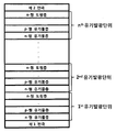
- FIG. 1 is a view showing an organic light emitting device according to an exemplary embodiment of the present invention.
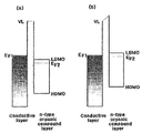
- FIG. 2 respectively show energy levels of the first electrode and the n-type organic compound layer before and after applying the n-type organic compound layer to the first electrode in the organic light emitting diode according to the exemplary embodiment of the present invention. The figure shown.
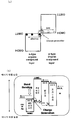
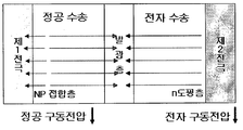
- FIG 3 is a view showing an NP junction formed between an n-type organic compound layer and a p-type organic compound layer in an organic light emitting device according to an exemplary embodiment of the present invention.
- FIG. 4 is a view showing the energy level of the organic light emitting device according to the prior art.
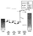
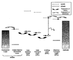
- FIG 5 is a view showing the energy level of the organic light emitting device according to an exemplary embodiment of the present invention.
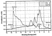
- FIG. 6 is a graph showing UPS (Ultraviolet Photoelectron Spectrum) data of a gold film and a HAT film positioned on the gold film.
- UPS Ultraviolet Photoelectron Spectrum
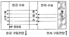
- FIG. 7 is a diagram illustrating the movement of electrons and holes in an organic light emitting device using only NP junction among NP junction and n-type doped organic material application techniques.
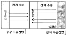
- FIG. 8 is a diagram illustrating the movement of electrons and holes in an organic light emitting device to which only n-type doped organic materials are applied among NP junction and n-type doped organic material application technologies.
- FIG. 9 is a diagram illustrating the movement of electrons and holes in an organic light emitting device to which both NP junction and n-type doped organic material application are applied.
- FIG. 10 is a diagram illustrating electron and hole movement of a stacked organic light emitting device in which two unit organic light emitting devices to which both an NP junction and an n-type doped organic material are applied are stacked.
- the stacked organic light emitting diode includes a first electrode, a second electrode, and at least two light emitting units positioned between the first electrode and the second electrode, wherein the light emitting unit has the following energy.
- An n-type organic compound layer and a p-type organic compound layer satisfying the relationship and forming an NP junction are included, and the n-type doped organic compound layer is included between the light emitting units.
- E nL is the lower unoccupied molecular orbital energy level of the n-type organic compound layer
- E pH is the highest occupied molecular orbital energy level of the p-type organic compound layer.
- NP junctions are formed in each light emitting unit.
- 3 shows an NP junction formed between the n-type organic compound layer and the p-type organic compound layer.
- the n-type organic compound layer preferably has a predetermined LUMO energy level with respect to the HOMO energy level of the p-type organic compound layer. If the HOMO level of the p-type organic material is smaller than the LUMO level of the n-type organic material, spontaneous charge generation may occur. For reference, the smaller the energy level is, the larger the energy value of the electron is. In order for spontaneous charge generation to occur, the HOMO level of the p-type organic material need only be small compared to the LUMO level of the n-type organic material, and the magnitude of the energy difference is not particularly limited.
- the vacuum level (VL) shift at the NP junction interface is possible about 1 eV, and the HOMO level of the p-type organic compound layer is changed to the LUMO level of the n-type organic compound layer under the condition that spontaneous charge can be generated. Compared to the energy level as large as 1 eV in comparison.
- the NP junction is not only physically in contact with the n-type organic compound layer and the p-type organic compound layer, but also must satisfy the above-described energy relationship.
- the charge injection barrier When the charge generating structure is applied to a unit organic light emitting device, the charge injection barrier is lowered to enable low voltage device driving.
- the charge generation layer having the NP junction structure may serve as a connection layer between two units of an organic light emitting diode when the stacked device is implemented to implement a stacked light emitting diode.
- Conventional organic light emitting devices use a method of directly injecting holes from the anode electrode into the HOMO level of the organic material, but in the present invention, the organic material layer is in contact with the anode electrode or the n-type doped organic material layer, and the n-type organic material having a large LUMO level is present.
- N-type and p-type organics were used to form NP junctions.
- charge generation is caused by the NP junction, and the transfer of electrons between the electrode or the n-type doped organic layer and the n-type organic compound layer is performed by LUMO of n-type organic material and n-type doped organic material. To move to the level.
- the n-type organic compound layer forming the NP junction in the light emitting unit in contact with the first electrode is in contact with the first electrode and satisfies the following energy relationship:
- E F1 is the Fermi energy level of the first electrode
- E nL is the lower unoccupied molecular orbital (LUMO) energy level of the n-type organic compound layer.
- the n-type organic compound layer forming the NP junction is preferably in contact with the n-type doped organic material layer.
- the first electrode is in contact with the NP junction structure, more various materials may be used than the material that can be used as the conventional electrode material.
- a material including a metal, a metal oxide, or a conductive polymer and an n-type doped organic material may be used as the first electrode.
- the conductive polymer may include an electrically conductive polymer.
- the first electrode may be formed of the same material as the second electrode.
- the NP junction structure not only functions as an intermediate connector together with the n-type doped organic material layer in the stacked device, but also, when the NP junction is used in each unit light emitting device, it is possible to implement a low voltage long life device. Therefore, when each unit light emitting device includes a charge generating layer having an NP junction structure, when the unit light emitting device including the charge generating layer is simply repeated n times, the stacked light emitting device in which n unit light emitting devices are stacked may be provided. have. As a result, the stacked light emitting device may be formed in a repeating structure of the unit light emitting device without an additional intermediate connection layer, thereby simplifying the process of the stacked device.
- the NP junction is used as the layer in contact with the first electrode, the low voltage driving and long life stacking type devices of the n-type light emitting devices are stacked, compared to the stacked devices having n-1 intermediate connector layers including the NP junctions. Implementation is possible.
- the Fermi level of the first electrode and the LUMO level of the n-type organic compound layer should have a value such that the electrons generated at the NP junction and the electrons of the LUMO level of the n-type organic compound layer in the holes can move to the first electrode.
- the charge transfer due to a change in vacuum level (VL), gap state or dipole formation as free electrons of the first electrode move to the LUMO level of the n-type organic layer at the interface between the first electrode and the n-type organic compound layer. This becomes possible.
- the energy difference between the Fermi level of the first electrode and the LUMO level of the n-type organic compound layer may be more preferably about 0.01 to 4 eV from the viewpoint of material selection. If the energy difference between the LUMO energy level of the n-type organic compound layer and the Fermi energy level of the first electrode is greater than 4 eV, the effect of surface dipole or gap state on the energy barrier of hole injection is Decreases.
- the p-type organic compound layer may include a hole injection layer, a hole transport layer, or a light emitting layer.
- the first electrode may include a conductive layer.
- the conductive layer includes a metal, a metal oxide, or a conductive polymer and an n-type doped organic material.
- the conductive polymer may include an electrically conductive polymer.
- the first electrode may be formed of the same material as the second electrode.
- each light emitting unit may include at least one light emitting layer.
- the organic light emitting device according to the present invention may include an additional organic material layer in addition to the aforementioned organic material layer.
- the organic light emitting device according to the present invention further includes one or more organic material layers, they may be formed of the same material or different materials.
- the organic light emitting diode according to the present invention includes two or more light emitting units between the first electrode and the second electrode, and the light emitting unit satisfies the above-described energy relationship and forms an n-type organic compound layer and p ⁇ . It includes a type organic compound layer, and between the light emitting unit comprises an n- type doped organic material layer. Each of the light emitting units may further include an organic material layer including at least one light emitting layer.
- the first electrode is shown as a lower electrode in FIG. 1, the first electrode is the upper electrode and the second electrode is also included in the present invention.
- the stacked organic light emitting device according to the present invention may include two or three or more light emitting units.
- the number of the laminated structure can be selected as needed, the upper limit of the number is not particularly limited.
- FIG. 2A the first electrode has a Fermi energy level E F1 that is smaller than the LUMO energy level E nL of the n-type organic compound layer.
- the vacuum level VL represents an energy level at which electrons can be drawn out of the first electrode and the n-type organic compound layer.
- the energy barrier for hole injection can be reduced by contacting the first electrode and the n-type organic compound layer.
- the first electrode has a Fermi energy level smaller than the LUMO energy level of the n-type organic compound layer, electrons move from the first electrode to the n-type organic compound layer at the interface between the first electrode and the n-type organic compound layer. Form a gap state. Thus, the energy barrier for electron transport is minimized.
- the stacked organic light emitting device includes an n-type doped organic material layer between the light emitting units.
- the n-type doping may be achieved by doping a suitable donor material to the organic material layer, whereby the density of charge carriers in the organic material layer may be greatly increased, and thus the conductivity of the charge may be greatly increased.
- balancing in the light emitting area of each light emitting unit can be achieved.
- balancing means recombination in the emission region to make the density of the holes and electrons participating in the emission maximized and the same.
- the organic light emitting device according to the present invention can exhibit much better low voltage, high brightness and high efficiency characteristics.
- the energy barrier for hole injection may be greatly lowered by NP junction of the n-type organic compound layer and the p-type organic compound layer.
- hole injection and transport from the first electrode to the light emitting region of the organic light emitting diode can be efficiently performed.
- the organic light emitting device according to the present invention having high hole injection efficiency, when n-type doping of an organic material or an inorganic material to an organic material layer improves electron transport ability, not only holes but also electrons are also present in the light emitting region of the device at a high concentration. Can be reached.
- the organic light emitting device according to the present invention can exhibit a much better low voltage, high brightness and high efficiency characteristics because a plurality of light emitting units are stacked without the insertion of the intermediate conductive layer.
- the light emitting unit in contact with the second electrode further includes an n-type doped organic material layer.
- the n-type doped organic material layer included in the light emitting unit contacting the second electrode may be an electron injection layer, an electron transport layer, or an electron injection and transport layer.
- charge balancing may be more efficiently achieved in the light emitting region of each light emitting unit.
- FIG. 7 is a diagram illustrating electron and hole movement of an organic light emitting diode using only NP junction among NP junction and n-type doped organic layer application techniques.
- the organic light emitting device using only the NP junction improves only the hole injection and transport characteristics, so that the concentration of holes in the light emitting layer is relatively higher than that of electrons. Will be lowered.
- the driving voltage decreases due to the improvement of the hole injection and transport characteristics, but the emission luminance decreases. Therefore, the increase in the emission efficiency, which is a watt ratio expressed by the product of the current voltage to the emission luminance, can be expected. none.
- FIG. 8 is a diagram illustrating electron and hole movement of an organic light emitting diode to which only an n-type doped organic material is applied among NP junction and n-type doped organic layer application technologies.
- the organic light emitting device using only n-type organic material doping among NP junction and n-type doped organic material application technology only electron injection and transport characteristics are improved, so the concentration of electrons in the light emitting layer is relatively higher than that of holes. Balancing is reduced.
- FIG. 9 is a diagram illustrating the movement of electrons and holes in an organic light emitting device to which both an NP junction and an n-type doped organic material layer are applied.
- the NP junction and the n-type doped organic material are used at the same time, the hole injection and transport characteristics of the NP junction and the electron injection and transport characteristics of the n-type doping are improved.
- the concentration of the holes is balanced, a large driving voltage is reduced due to the improvement of the charge injection and transport characteristics of the charge, and the brightness is improved by the balancing of the electrons and the holes. Therefore, it is possible to fabricate an organic light emitting device having high luminous efficiency, which is a Watt ratio expressed by the product of the current voltage to the luminous brightness.
- FIG. 10 illustrates a stacked organic light emitting device in which each light emitting unit includes an NP junction structure, and a first electrode is in contact with the NP junction structure, and an n-doped organic layer is applied as the organic layer between the light emitting units and between the second electrode. The case is illustrated.
- the n-time repeating structure of the unit organic light emitting diodes between the first electrode and the second electrode it is possible to manufacture the stacked high efficiency stacked device stacked n times.
- an organic material or an inorganic material may be used as a material for n-type doping of the n-type doped organic material layer.
- the inorganic materials include alkali metals such as lithium (Li), sodium (Na), potassium (K), rubidium (Rb), cesium (Cs), and the like; Alkaline earth metals such as beryllium (Be), magnesium (Mg), calcium (Ca), strontium (Sr), barium (Ba), and radium (Ra), La, Ce, Pr, Nd, Sm, Eu, Tb, Th, Dy, Ho, Er, Em, Gd, Yb, Lu, Y, Mn Or a metal compound containing at least one of these metals.
- Alkali metals such as lithium (Li), sodium (Na), potassium (K), rubidium (Rb), cesium (Cs), and the like
- Alkaline earth metals such as beryllium (Be), magnesium (Mg), calcium (Ca), strontium (S
- the organic material is cyclopentadiene, cycloheptatriene, six-membered heterocyclic ring or an organic material containing a condensed ring containing these rings, specifically xanthene-based, acridine-based, diphenylamine-based, azine-based, jade
- Organic materials such as photographic, thiazine-based or thioxanthene-based may be used.
- 2,3,5,6-tetrafluoro-7,7,8,8-tetracyanoquinomimethane (F4TCNQ) or the like may be used as the doped organic material.
- the n-type doping concentration is preferably from 0.02 to 50% by volume.
- the thickness of the n-type doped organic material layer is preferably less than 500 GPa, and when used thicker than this, the luminous efficiency may be reduced by absorbing visible light by the n-type doping material. More preferably, less than 100 GPa is preferable.
- the thickness of the n-type doped organic material layer may be formed to 10 ⁇ or more.
- the formation of the n-type doped organic material layer by an organic material or an inorganic material may be made using a method known in the art, and the scope of the present invention is not limited by a specific method.
- an organic salt such as HCl salt of pyronin B
- an organic glucobase which is then doped by evaporation with the organic to be doped under vacuum in which the substrate to form the doped organic layer is present.
- the formed organic material layer can be formed.
- the organic material to be doped such as tetrafluorotetracyanoquinomethane (TCNQ)
- TCNQ tetrafluorotetracyanoquinomethane
- a dopant dimer such as di- (p-methoxyphenylamine) methyl.
- doped to form a doped organic material layer by irradiating with light to oxidize the dimer and transfer electrons to TCNQ.
- a non-charged state such as hydrogenated form
- the organic material in the hydrogenated form can be prepared independently in the absence of the organic material layer to which it is to be doped.
- the organic substance in the hydrogenated form may be prepared by sublimating a salt of the organic substance. If necessary, further purification may be carried out to improve the yield and purity of the organics in the hydrogenated form, and the organics in the hydrogenated form are preferably used in a purified state.
- the organics in hydrogenated form can be injected directly into the doped organic layer, for example by mixed evaporation or continuous evaporation with the organic layer material to be doped.
- Organics in the hydrogenated form are nonionic neutral molecules and thus exhibit almost complete sublimation. Therefore, the sublimation of the organic substance in the hydrogenated form also has the same effect as the evaporation of the organic substance in the hydrogenated form.
- the cation or radical of the organic material may be formed by separating hydrogen, carbon monoxide, nitrogen, or hydroxy radicals from the hydrogenated organic material.
- the separation may be made by light or electron beam irradiation.
- the radiation spectrum used for the irradiation of light is preferably at least partially overlapping with the absorption region of any of the non-charged organics in the hydrogenated form and the organic layer material doped.
- N-type doping may be achieved by transferring electrons from the radicals formed as described above to the doped organic material.
- the hydrogen, carbon monoxide, nitrogen or hydroxy radicals can be separated from cyclopentadiene, cycloheptatriene or 6 membered hetero ring of organic matter.
- electron emission n-type doping takes place by the formation of a 6 pi-aromatic system.
- the electron emission or acceptance is 8 pi-, 10 pi-, 12 pi-, or (2n Pi (n is an integer of 7 or more).
- the organic substance in the hydrogenated form may be a carbinol base or leuco base of a cationic dye.
- Cationic dyes are generally known to have high quantum efficiency with respect to the light output of the organic light emitting device.
- a cationic dye such as rhodamine B, exhibits high luminous quantum efficiency when used as a light emitting dopant in an organic light emitting device.
- xanthene dye As the cationic dye, xanthene dye, acridine dye, diphenylamine dye, azine dye, oxazine dye, thiazine dye or thioxanthene dye may be used, but is not limited thereto.
- compounds that can be converted into cations by separation of functional groups composed of hydrides can also be used as the cationic dye.
- the material of the doped organic material layer is not particularly limited, but an electron injection or transport material may be used.
- a compound having a functional group selected from imidazole group, oxazole group, thiazole group, quinoline and phenanthrosine group can be used.
- the compound having a functional group selected from the imidazole group, the oxazole group and the thiazole group include compounds of the compound of formula 1 or 2 below:
- R 1 to R 4 may be the same or different from each other, and each independently a hydrogen atom; Halogen atom, amino group, nitrile group, nitro group, C 1 ⁇ C 30 alkyl group, C 2 ⁇ C 30 alkenyl group, C 1 ⁇ C 30 alkoxy group, C 3 ⁇ C 30 cycloalkyl group, C 3 ⁇ C A C 1 -C 30 alkyl group substituted or unsubstituted with one or more groups selected from the group consisting of 30 heterocycloalkyl groups, C 5 -C 30 aryl groups and C 2 -C 30 heteroaryl groups; Halogen atom, amino group, nitrile group, nitro group, C 1 ⁇ C 30 alkyl group, C 2 ⁇ C 30 alkenyl group, C 1 ⁇ C 30 alkoxy group, C 3 ⁇ C 30 cycloalkyl group, C 3 ⁇ C A C 3 -C 30 cycloalkyl group substituted or unsubstitute
- X is O, S, NR b or a C 1 -C 7 divalent hydrocarbon group
- A, D and R b each represent a hydrogen atom, a nitrile group (-CN), a nitro group (-NO 2 ), an alkyl of C 1 -C 24 , an aromatic ring of C 5 -C 20 or a substituted hetero atom
- Alkylene comprising an alkylene or hetero atom capable of forming a fused ring with an aromatic ring, a halogen, or an adjacent ring
- a and D may be joined to form an aromatic or heteroaromatic ring
- B is a substituted or unsubstituted alkylene or arylene that connects a plurality of hetero rings to be conjugated or unconjugated as n is 2 or more, and when n is 1, substituted or unsubstituted alkyl or aryl; n is an integer from 1 to 8.
- Examples of the compound of Formula 1 include compounds known from Korean Patent Publication No. 2003-0067773, and examples of the compound of Formula 2 include compounds described in US Pat. No. 5,645,948 and compounds described in WO05 / 097756. Include. The above documents are all incorporated herein by reference.
- the compound of Formula 1 also includes a compound of Formula 3:
- R 5 to R 7 are the same as or different from each other, and are each independently a hydrogen atom, an aliphatic hydrocarbon of C 1 -C 20 , an aromatic ring, an aromatic hetero ring, or an aliphatic or aromatic condensed ring;
- Ar is a direct bond, an aromatic ring, an aromatic hetero ring or an aliphatic or aromatic condensed ring;
- X is O, S or NR a ;
- R a is a hydrogen atom, an aliphatic hydrocarbon of C 1 -C 7 , an aromatic ring or an aromatic hetero ring; Except where R 5 and R 6 are hydrogen at the same time.
- the compound of Formula 2 also includes a compound of Formula 4:
- Z is O, S or NR b ;
- R 8 and R b may form a fused ring with a hydrogen atom, a C 1 -C 24 alkyl, a C 5 -C 20 aromatic ring or a substituted aromatic ring containing a hetero atom, a halogen, or a benzazole ring Alkylene or alkylene containing hetero atoms;
- B is an alkylene, arylene, substituted alkylene, or substituted arylene that connects a plurality of benzazoles to be conjugated or non-conjugated as a connecting unit when n is 2 or more, and when n is 1, substituted or unsubstituted Alkyl or aryl;
- n is an integer from 1 to 8.
- Preferred compounds having imidazole groups include compounds of the following structure:
- Examples of the compound having a quinoline group include compounds represented by the following Chemical Formulas 5 to 11.
- n is an integer from 0 to 9
- m is an integer of 2 or more
- R 9 is an alkyl group such as hydrogen, a methyl group, an ethyl group, a cycloalkyl group such as cyclohexyl, norbornyl, an aralkyl group such as benzyl group, an alkenyl group such as vinyl group, allyl group, cyclopentadienyl group, cyclohexenyl group, etc.
- Alkoxy groups such as cycloalkenyl groups and methoxy groups
- Alkylthio groups in which the oxygen atom of the ether bond of an alkoxy group is substituted by the sulfur atom
- Aryl ether groups such as the phenoxy group, and aryl in which the oxygen atom of the ether bond of the arylether group is substituted by the sulfur atom
- Heterocyclic groups such as aryl groups, such as a thioether group, a phenyl group, a naphthyl group, and a biphenyl group, a furyl group, a thienyl group, an oxazolyl group, a pyridyl group, a quinolyl group, and a carbazolyl group, a halogen, a cyano group, an aldehyde group, and a carbonyl group , Silyl groups such as carboxyl group, ester group, carbamoyl group, amino group,
- Y is a divalent or higher group of the groups of R 9 .
- Examples of the compound having a phenanthrosine group include compounds represented by the following Chemical Formulas 12 to 22, but are not limited thereto.
- n + p is 8 or less
- R ⁇ 10> and R ⁇ 11> are hydrogen, methyl, alkyl groups, such as an ethyl group, cycloalkyl groups, such as cyclohexyl and norbornyl, aralkyl groups, such as benzyl, alkenyl groups, such as a vinyl group and an allyl group, and cyclo Alkyl groups, such as cycloalkenyl groups, such as a pentadienyl group and a cyclohexenyl group, and a methoxy group, Alkylthio group, such as the arylether group, and the arylether group in which the oxygen atom of the ether bond of the alkoxy group was substituted by the sulfur atom, etc.
- Heterocyclic groups such as the aryl group which the oxygen atom of a bond substituted by the sulfur atom, the aryl group, such as a phenyl group, a naphthyl group, and a biphenyl group, a furyl group, a thienyl group, an oxazolyl group, a pyridyl group, a quinolyl group, and a carbazolyl group , Silyl group such as halogen, cyano group, aldehyde group, carbonyl group, carboxyl group, ester group, carbamoyl group, amino group, nitro group and trimethylsilyl group, siloxanyl group which is a group having silicon through ether bond And a ring structure that is formed of a group;
- R 10 is a direct bond or a divalent or more group of the aforementioned groups, and R 11 is the same as when m is 1,
- the substituents may be unsubstituted or substituted, and when n or p is 2 or more, the substituents may be the same or different from each other.
- R 1a to R 8a and R 1b to R 10b each represent a hydrogen atom, a substituted or unsubstituted aryl group having 5 to 60 nuclear atoms, a substituted or unsubstituted pyridyl group, a substituted or unsubstituted qui Nolyl group, substituted or unsubstituted 1-50 alkyl group, bicyclic or unsubstituted cycloalkyl group having 3-50 carbon atoms, substituted or unsubstituted aralkyl group having 6-50 nuclear atoms, substituted or unsubstituted alkoxy group having 1-50 carbon atoms , Substituted or unsubstituted aryloxy group having 5-50 nuclear atoms, substituted or unsubstituted arylthio group having 5-50 nuclear atoms, substituted or unsubstituted alkoxycarbonyl group having 1-50 carbon atoms, substituted or unsubstitute
- d 1 , d 3 to d 10 and g 1 are each a hydrogen or an aromatic or aliphatic hydrocarbon group, m and n are integers of 0 to 2, and p is an integer of 0 to 3.
- the compounds of Formulas 20 and 21 are described in US Patent Publication 2007/0122656, which is incorporated herein by reference in its entirety.
- R 1c to R 6c each represent a hydrogen atom, a substituted or unsubstituted alkyl group, a substituted or unsubstituted aralkyl group, a substituted or unsubstituted aryl group, a substituted or unsubstituted heterocyclic group or a halogen atom, and Ar 1c and Ar 2c is each selected from the following structural formula.
- R 17 to R 23 in the above structural formulas each represent a hydrogen atom, a substituted or unsubstituted alkyl group, a substituted or unsubstituted aralkyl group, a substituted or unsubstituted aryl group, a substituted or unsubstituted heterocyclic group or a halogen atom.
- the compound of formula 22 is described in Japanese Patent Laid-Open No. 2004-107263, which is incorporated by reference in its entirety.
- the stacked organic light emitting device according to the present invention can be manufactured in the above-described structure using a method known in the art.
- the material of each layer and the method of n-type doping are the same as described above, so the detailed description thereof will be omitted.
- 5 is a view illustrating an energy level of an organic light emitting device having one light emitting unit in order to describe an energy level of the stacked organic light emitting device according to an exemplary embodiment of the present invention.
- 5 includes an anode, an n-type organic compound layer, a p-type hole injection layer (HIL), a hole transport layer (HTL), an emission layer (EML), an electron transport layer (ETL), and a cathode.
- HIL hole injection layer
- HTL hole transport layer
- EML emission layer
- ETL electron transport layer
- cathode The energy difference between the LUMO energy level of the n-type organic compound layer and the Fermi energy level of the anode is about 4 eV or less, and the LUMO energy level of the n-type organic compound layer and the HOMO energy level of the p-type hole injection layer are Satisfies the energy relationship.
- the anode may be formed of various conductive materials.
- the anode may be formed of the same material as the cathode.
- an organic light emitting device in which the conductive material has a low work function can be manufactured.
- the hole and electron transporting ability can be improved by the above-described configuration, so that the balancing of holes and electrons can be achieved.
- the electron injection layer made of a material such as LiF is not provided, an electron injection like the LiF layer can be achieved. Better device performance can be achieved than with layers.
- the organic material layer n-doped with alkaline earth metal may contact the second electrode.
- the electron injection layer not including the electron injection layer in the scope of the present invention.
- the present invention can provide a stack type organic light emitting device having high efficiency and high brightness on the same principle as described above.
- the organic light emitting diode since the luminance increases in proportion to the number of organic light emitting diode units stacked under the same driving voltage, the organic light emitting diode may be stacked to obtain a high luminance organic light emitting diode.
- the stacked organic light emitting diode according to the present invention may have an inverted structure in which a cathode, an organic material layer, and an anode are sequentially stacked from below on a substrate. That is, in the stacked organic light emitting diode according to the present invention, when the first electrode is an anode and the second electrode is a cathode, the second electrode is a lower electrode positioned on a substrate, and the first electrode is an upper electrode. Can be.
- the stacked organic light emitting diode according to the present invention may have a normal structure in which an anode, an organic material layer, and a cathode are sequentially stacked from below on a substrate. That is, when the first electrode is an anode and the second electrode is a cathode, the first electrode may be a lower electrode positioned on a substrate, and the second electrode may be an upper electrode.
- each layer constituting the organic light emitting device will be described in detail.
- the materials of each layer described below may be a single material or a mixture of two or more materials.
- the first electrode includes a conductive layer.
- the conductive layer comprises a metal, a metal oxide or a conductive polymer.
- the conductive polymer may include an electrically conductive polymer.
- the first electrode may be formed of various conductive materials. For example, it has a Fermi energy level of about 2 to 5.5 eV. In the conventional organic light emitting device, only materials having a Fermi energy level of 5 to 6 eV can be used as the first electrode, but in the present invention, a material having a Fermi energy level of 2 to 5 eV, particularly a material having 2 to 4 eV, may be used.
- Examples of exemplary conductive materials include carbon, cesium, potassium, lithium, calcium, sodium, magnesium, nironium, indium, aluminum, silver, tantalum, vanadium, chromium, copper, zinc, iron, tungsten, molybdenum, nickel, gold, Other metals and alloys thereof; Zinc oxide, indium oxide, tin oxide, indium tin oxide (ITO), indium zinc oxide and other similar metal oxides; And mixtures of oxides and metals such as ZnO: Al and SnO 2 : Sb.
- the organic light emitting device is a top emission type, not only a transparent material but also an opaque material having excellent light reflectance may be used as the conductive layer. In the case of the back light-emitting organic light emitting device, it should be a transparent material as the first electrode, and if an opaque material is used, it should be formed into a thin film so as to be transparent.
- the surface of the conductive layer may be treated with nitrogen plasma or oxygen plasma.
- the Fermi level of the first electrode due to the plasma treatment is increased during the oxygen plasma treatment, and lowered in the nitrogen plasma treatment.
- the conductivity of the first electrode can be increased, and nitride can be formed on the surface while lowering the surface oxygen concentration, thereby increasing the life of the device.
- the Fermi level of the first electrode is lowered, making it difficult to inject holes, thereby increasing the driving voltage.
- the NP junction structure as in the present invention, even if the Fermi level of the first electrode is lowered, there is no effect on the hole injection characteristics due to the NP junction, so that nitrogen plasma treatment is possible, and thus, a device having a long life and low voltage. Implementation is possible.
- the stacked organic light emitting diode according to the present invention includes two or more light emitting units positioned between the first electrode and the second electrode, and each of the light emitting units includes an n-type organic material layer and a p-type organic material layer forming NP junctions, respectively.
- the stacked organic light emitting diode according to the present invention includes an n-type doped organic material layer between the light emitting units, and if necessary, includes an n-type doped organic material layer as an organic material layer contacting the second electrode.
- the n-type organic compound layer injects holes into the organic compound layer in a low electric field.
- the n-type organic compound layer preferably has a LUMO energy level of about 4 ⁇ 7eV, about 10 -8 cm 2 / Vs ⁇ 1 cm 2 / Vs, preferably about 10 -6 cm 2 / Vs ⁇ 10 -2 It is desirable to have an electron mobility of cm 2 / Vs. If the electron mobility is less than about 10 -8 cm 2 / Vs it is not easy to inject holes. If the electron mobility exceeds 1 cm 2 / Vs, the hole injection becomes more efficient, but such a material is typically a crystalline organic material, so it is difficult to apply to an organic light emitting device using an amorphous organic material.
- the n-type organic compound layer may be formed of a material that can be vacuum deposited or a material that can be thin-film formed by a solution process.
- Specific examples of the n-type organic material include, but are not limited to, 2,3,5,6-tetrafluoro-7,7,8,8-tetracyanoquinomimethane (F4TCNQ), fluorine-substituted 3, 4,9,10-perylenetetracarboxylic dianhydride (PTCDA), cyano-substituted PTCDA, naphthalenetetracarboxylic dianhydride (NTCDA), fluorine-substituted NTCDA, cyano-substituted NTCDA Or a compound of Formula 23:
- R 1 to R 6 each represent hydrogen, a halogen atom, nitrile (-CN), nitro (-NO 2 ), sulfonyl (-SO 2 R), sulfoxide (-SOR), and sulfonamide ( -SO 2 NR), sulfonate (-SO 3 R), trifluoromethyl (-CF 3 ), ester (-COOR), amide (-CONHR or -CONRR '), substituted or unsubstituted straight or branched chain C 1 -C 12 alkoxy, substituted or unsubstituted straight or branched chain C 1 -C 12 alkyl, substituted or unsubstituted aromatic or non-aromatic hetero ring, substituted or unsubstituted aryl, substituted or unsubstituted Mono- or di-arylamine, and substituted or unsubstituted aralkylamine, wherein R and R 'are each substituted or unsubstituted
- the compound of Chemical Formula 23 may be exemplified by the compound of Chemical Formulas 23-1 to 23-6.
- the light emitting units may further include one or more organic material layers including a hole injection layer, a hole transport layer, a light emitting layer, an electron transport layer, and an electron injection layer.
- the hole injection layer or the hole transport layer may be formed of a p-type organic compound layer.
- the p-type hole injection layer or the p-type hole transport layer may form an NP junction with the n-type organic compound layer, and holes formed in the NP junction may be formed through the p-type hole injection layer or the p-type hole transport layer. Transported to the light emitting layer.
- the HOMO energy level of the p-type hole injection layer or the p-type hole transport layer and the LUMO energy level of the n-type organic compound layer satisfy an energy relationship of the following equation.
- E pH -E nL ⁇ 1 eV preferably E pH -E nL ⁇ 0.5 eV
- the p-type hole injection layer or the p-type hole transport layer may include, but is not limited to, an arylamine-based compound, a conductive polymer, or a block copolymer having a conjugated portion and a non-conjugated portion.
- the light emitting layer since hole and electron transfer occur at the same time, the light emitting layer may have both n-type and p-type characteristics.
- the electron transport may be defined as an n-type light emitting layer faster than the hole transport, and the hole transport may be defined as a p-type light emitting layer faster than the electron transport.
- n-type light emitting layer since electron transport is faster than hole transport, light emission occurs near the interface between the hole transport layer and the light emitting layer. Therefore, when the LUMO level of the hole transport layer is higher than the LUMO level of the light emitting layer, it may exhibit better light emission efficiency.
- the n-type light emitting layer is not limited thereto, but may include aluminum tris (8-hydroxyquinoline) (Alq 3 ); 8-hydroxyquinoline beryllium (BAlq); Benzoxazole compound, benzthiazole compound or benzimidazole compound; Polyfluorene-based compounds; Silacyclopentadiene (silole) compounds and the like.
- the hole transport is faster than the electron transport, light emission occurs near the interface between the electron transport layer and the light emitting layer. Therefore, when the HOMO level of the electron transport layer is lower than the HOMO level of the light emitting layer, it may exhibit better light emission efficiency.
- the effect of increasing the luminous efficiency due to the change in the LUMO level of the hole transport layer is smaller than in the case of using the n-type light emitting layer. Therefore, when the p-type light emitting layer is used, an organic light emitting device having an NP junction structure between the n-type organic compound layer and the p-type light emitting layer can be manufactured without using the hole injection layer and the hole transport layer.
- the p-type light emitting layer is not limited thereto, but includes a carbazole compound; Anthracene-based compounds; Polyphenylenevinylene (PPV) -based polymers; Or spiro compounds and the like.
- the electron transport layer material a material having high electron mobility is preferable so that electrons can be well injected from the cathode and transported well to the light emitting layer.
- the electron transport layer is not limited thereto, but may include aluminum tris (8-hydroxyquinoline) (Alq 3); Organic compounds containing Alq 3 structures; Hydroxyflavone-metal complex compounds or silacyclopentadiene (silole) compounds.
- the second electrode material a material having a small work function is generally preferred to facilitate electron injection into the organic material layer.
- the second electrode may include, but is not limited to, metals such as magnesium, calcium, sodium, potassium, titanium, indium, yttrium, lithium, gadolinium, aluminum, silver, tin, and lead or alloys thereof; Multilayer structure materials such as LiF / Al or LiO 2 / Al, and the like.
- the second electrode may be formed of the same material as the first electrode.
- the second electrode or the first electrode may comprise a transparent material.
- Hexanitrile hexaazatriphenylene was used as an organic material of n-type semiconductor properties.
- Ultraviolet photoelectron spectroscopy (UPS) was used to measure the HOMO level of the HAT. This method analyzes the kinetic energy of electrons from the sample when the sample is irradiated with vacuum UV rays (21.20eV) from the He lamp under ultra-vacuum (10 -8 Torr). In this case, the ionization energy, that is, the HOMO level and the Fermi energy level can be determined.
- the kinetic energy of the electrons emitted from the sample is the difference between the vacuum UV energy 21.2 eV and the electron binding energy of the sample to be measured. Therefore, by analyzing the kinetic energy distribution of electrons emitted from the sample it is possible to know the distribution of binding energy in the molecule of the material in the sample. At this time, when the maximum energy value of the kinetic energy of the electron has a minimum binding energy of the sample. This can be used to determine the work function (Fermi energy level) and HOMO level of the sample.
- FIG. 7 shows UPS data from the gold film and the HAT film having a thickness of 20 nm thereon. The following description is made using terms used in H. Ishii, et al., Advanced Materials, 11, 605-625 (1999).
- the binding energy (eV) of the x-axis is a value calculated based on a work function measured in a gold film. That is, in this measurement, the work function of gold was measured as 5.28 eV, which is the value of irradiated light energy (21.20 eV) minus the maximum value of the binding energy (15.92 eV).
- the HAT defined by subtracting the difference between the maximum value (15.21 eV) and the minimum value (3.79 eV) of the binding energy from the light energy irradiated on the HAT deposited on the gold film has a HOMO level of 9.78 eV and a Fermi energy level of 6.02 V to be.
- IZO was sputtered on the substrate to form a 1000 nm thick transparent anode (first electrode), and a vacuum HAT was deposited thereon to form an n-type organic material having a thickness of 500 mW, and thereon, NPB having the following formula
- the vacuum deposition was carried out to form a hole transport layer having a thickness of 400 kPa to form NP junctions.
- BAlq which is a hole blocking layer material of the following formula, was formed thereon to a thickness of 50 kPa.
- An electron transport layer material of the following formula was formed thereon at a thickness of 150 kPa, and 10 wt% of Ca was doped into the electron transport material of the following formula, thereby forming a doped electron transport layer having a thickness of 50 kPa.
- a unit organic light emitting device was manufactured by forming aluminum as a reflective cathode (second electrode) on the doped electron transport layer to a thickness of 1000 ⁇ .
- the device structure is IZO / HAT / NPB / CBP + Ir (ppy) 3 / BAlq / ETL / Ca + ETL / Al.
- the deposition rate of the organic material was maintained at 0.5 ⁇ 1.0 ⁇ / sec, the vacuum during deposition was maintained at about 2 x 10 -7 ⁇ 2 x 10 -8 torr.
- IZO was sputtered on the substrate to form a 1000 nm thick transparent anode (first electrode), and a vacuum HAT was deposited thereon to form an n-type organic material having a thickness of 500 mW, and thereon, NPB having the following formula
- the vacuum deposition was carried out to form a hole transport layer having a thickness of 400 kPa to form NP junctions.
- BAlq which is a hole blocking layer material of the following formula, was formed thereon to a thickness of 50 kPa.
- the electron transport layer material of the following formula is formed thereon to a thickness of 150 kPa, 10 wt% Ca is doped into the electron transport material of the following formula, and the doped electron transport layer is formed to a thickness of 50 kPa, HAT / NPB / CBP + A unit device structure of Ir (ppy) 3 / BAlq / ETL / Ca + ETL was made. Two unit light emitting devices are stacked by forming a HAT / NPB / CBP + Ir (ppy) 3 / BAlq / ETL / Ca + ETL unit device layer on the doped Ca electron transport layer in the same method and thickness as the above method of depositing a unit device.
- the deposition rate of the organic material was maintained at 0.5 ⁇ 1.0 ⁇ / sec, the vacuum degree during deposition was maintained at about 2 x 10 -7 ⁇ 2 x 10 -8 torr.
- a stacked organic light emitting diode was manufactured according to the same method as Example 3 except for using Mg volume 10% instead of Ca as the n-type doped electron transport layer.
- the stacked device structure is IZO / NPB / CBP + Ir (ppy) 3 / BAlq / ETL / Mg + ETL / HAT / NPB / CBP + Ir (ppy) 3 / BAlq / ETL / Mg + ETL / Al.
- the stacked organic device structure is IZO / NPB / CBP + Ir (ppy) 3 / BAlq / ETL / Ca + ETL / HAT / NPB / CBP + Ir (ppy) 3 / BAlq / ETL / Ca + ETL / Al.
- a stacked organic light emitting diode was manufactured according to the same method as Example 2 except for depositing a thickness of the electron transport layer of the light emitting diode at 200 ⁇ s and depositing 15 ⁇ s of LiF on the electron injection layer.
- the stacked organic device structure is IZO / NPB / CBP + Ir (ppy) 3 / BAlq / ETL / Ca + ETL / HAT / NPB / CBP + Ir (ppy) 3 / BAlq / ETL / LiF / Al.
- an efficient organic light emitting device can be manufactured by using a charge generation layer formed by n NP junctions and n n-type doped organic materials in a stacked device in which n unit light emitting devices are stacked.
Landscapes
- Physics & Mathematics (AREA)
- Optics & Photonics (AREA)
- Chemical & Material Sciences (AREA)
- Engineering & Computer Science (AREA)
- Materials Engineering (AREA)
- Organic Chemistry (AREA)
- Electroluminescent Light Sources (AREA)
- Nitrogen Condensed Heterocyclic Rings (AREA)
Abstract
Description


| @10mA/cm2 | 구동 전압(V) | 전류 효율(cd/A) | 파워 효율(lm/W) |
| 실시예 2 | 8.5 | 98 | 36.2 |
| 실시예 3 | 9.3 | 96 | 32.4 |
| 비교예 1 | 4.5 | 52 | 36.3 |
| 비교예 2 | 14.2 | 100 | 22.1 |
| 비교예 3 | 15.2 | 92 | 19.0 |
Claims (17)
- 제 1 전극, 제2 전극, 및 상기 제1 전극과 제2 전극 사이에 위치하는 2 이상의 발광유닛을 포함하는 적층형 유기발광소자에 있어서, 상기 발광유닛은 하기 에너지 관계를 만족하고 NP 접합을 형성하는 n-형 유기물층 및 p-형 유기물층을 포함하고, 상기 발광유닛들 사이에는 n-형 도핑된 유기물층을 포함하는 것을 특징으로 하는 적층형 유기발광소자:EpH - EnL ≤ 1eV상기 식에 있어서, EnL은 상기 n-형 유기물층의 LUMO(lowest unoccupied molecular orbital) 에너지 준위이며, EpH는 상기 p-형 유기물층의 HOMO(highest occupied molecular orbital) 에너지 준위이다.
- 청구항 1에 있어서, 상기 제1 전극과 접하는 발광유닛에서 상기 NP 접합을 형성하는 n-형 유기물층은 상기 제1 전극과 접하고, 하기 에너지 관계를 만족하는 것인 적층형 유기발광소자:0eV < EnL - EF1 ≤ 4eV상기 식에 있어서, EF1은 상기 제1 전극의 페르미 에너지 준위이고, EnL은 상기 n-형 유기물층의 LUMO(lowest unoccupied molecular orbital) 에너지 준위이다.
- 청구항 1에 있어서, 상기 제1 전극과 접하는 발광유닛 이외의 발광유닛에서, 상기 NP 접합을 형성하는 n-형 유기물층은 상기 n-형 도핑된 유기물층과 접하는 것인 적층형 유기발광소자.
- 청구항 1에 있어서, 상기 제2 전극과 접하는 발광유닛은 n-형 도핑된 유기물층을 추가로 포함하는 것인 적층형 유기발광소자.
- 청구항 4에 있어서, 상기 n-형 도핑된 유기물층은 상기 제2 전극에 접하는 것인 적층형 유기발광소자.
- 청구항 1 내지 청구항 4 중 어느 하나의 항에 있어서, 상기 발광유닛들은 각각 적어도 하나의 발광층을 포함하는 것인 적층형 유기발광소자.
- 청구항 1 내지 청구항 4 중 어느 하나의 항에 있어서, 상기 n-형 도핑된 유기물층에 있어서 n-형 도핑 물질은 알칼리 금속, 알칼리 토금속, La, Ce, Pr, Nd, Sm, Eu, Tb, Th, Dy, Ho, Er, Em, Gd, Yb, Lu, Y 및 Mn로 이루어진 군으로부터 선택되는 1 이상의 금속 또는 상기 1 이상의 금속을 포함하는 금속 화합물을 포함하는 것인 적층형 유기발광소자.
- 청구항 1 내지 청구항 4 중 어느 하나의 항에 있어서, 상기 n-형 도핑된 유기물층에 있어서 n-형 도핑 물질은 시클로펜타디엔, 시클로헵타트리엔, 6원 헤테로 고리 또는 이들 고리가 포함된 축합고리를 포함하는 물질인 것인 적층형 유기발광소자.
- 청구항 1 내지 청구항 4 중 어느 하나의 항에 있어서, 상기 n-형 도핑된 유기물층에 있어서 도핑되는 유기물은 이미다졸기, 옥사졸기, 티아졸기, 퀴놀린 및 페난쓰롤린기로부터 선택되는 작용기를 갖는 화합물인 것인 적층형 유기발광소자.
- 청구항 4에 있어서, 상기 제2 전극과 접하는 발광유닛에 포함된 n-형 도핑된 유기물층은 전자 주입층, 전자 수송층 또는 전자 주입 및 수송층인 것인 적층형 유기발광소자.
- 청구항 1 내지 청구항 4 중 어느 하나의 항에 있어서, 상기 p-형 유기물층은 정공 주입층, 정공 수송층, 또는 발광층인 것인 적층형 유기발광소자.
- 청구항 1 내지 청구항 4 중 어느 하나의 항에 있어서, 상기 n-형 유기물층은 4 내지 7 eV의 LUMO 에너지 준위를 갖는 것인 유기발광소자.
- 청구항 1 내지 청구항 4 중 어느 하나의 항에 있어서, 상기 n-형 유기물층은 2,3,5,6-테트라플루오로-7,7,8,8-테트라시아노퀴노디메탄(F4TCNQ), 불소-치환된 3,4,9,10-페릴렌테트라카르복실릭 디안하이드라이드(PTCDA), 시아노-치환된 PTCDA, 나프탈렌테트라카르복실릭 디안하이드라이드(NTCDA), 불소-치환된 NTCDA, 시아노-치환된 NTCDA, 및 하기 화학식 23의 화합물로 이루어진 군에서 선택되는 유기물을 포함하는 것인 적층형 유기발광소자:[화학식 23]
 상기 화학식 23에 있어서, R1 내지 R6은 각각 수소, 할로겐 원자, 니트릴(-CN), 니트로(-NO2), 술포닐(-SO2R), 술폭사이드(-SOR), 술폰아미드(-SO2NR), 술포네이트(-SO3R), 트리플루오로메틸(-CF3), 에스테르(-COOR), 아미드(-CONHR 또는 -CONRR'), 치환 또는 비치환된 직쇄 또는 분지쇄의 C1-C12 알콕시, 치환 또는 비치환된 직쇄 또는 분지쇄 C1-C12의 알킬, 치환 또는 비치환된 방향족 또는 비방향족의 헤테로 고리, 치환 또는 비치환된 아릴, 치환 또는 비치환된 모노- 또는 디-아릴아민, 및 치환 또는 비치환된 아랄킬아민으로 구성된 군에서 선택되며, 상기 R 및 R'는 각각 치환 또는 비치환된 C1-C60의 알킬, 치환 또는 비치환된 아릴 및 치환 또는 비치환된 5-7원 헤테로 고리로 이루어진 군에서 선택된다.
 - 청구항 1 내지 청구항 4 중 어느 하나의 항에 있어서, 상기 제1 전극은 양극이고, 상기 제2 전극은 음극인 것인 적층형 유기발광소자.
- 청구항 1 내지 청구항 4 중 어느 하나의 항에 있어서, 상기 유기발광소자는 기판 상에 음극, 유기물층 및 양극이 순차적으로 형성된 인버티드(inverted) 구조인 것인 적층형 유기발광소자.
- 청구항 1 내지 청구항 4 중 어느 하나의 항에 있어서, 상기 제1 전극과 상기 제2 전극은 동일한 물질로 형성된 것인 적층형 유기발광소자.
- 청구항 1 내지 청구항 4 중 어느 하나의 항에 있어서, 상기 제1 전극 및 상기 제2 전극 중 적어도 하나는 투명 물질을 포함하는 것인 적층형 유기발광소자.
Priority Applications (4)
| Application Number | Priority Date | Filing Date | Title |
|---|---|---|---|
| JP2011509421A JP2011521414A (ja) | 2008-05-16 | 2009-05-15 | 積層型有機発光素子 |
| US12/992,868 US8637854B2 (en) | 2008-05-16 | 2009-05-15 | Stacked organic light emitting diode |
| CN2009801178013A CN102067730A (zh) | 2008-05-16 | 2009-05-15 | 层叠式有机发光二极管 |
| EP09746786.4A EP2299786B1 (en) | 2008-05-16 | 2009-05-15 | Stacked organic light-emitting diode |
Applications Claiming Priority (2)
| Application Number | Priority Date | Filing Date | Title |
|---|---|---|---|
| KR20080045361 | 2008-05-16 | ||
| KR10-2008-0045361 | 2008-05-16 |
Publications (2)
| Publication Number | Publication Date |
|---|---|
| WO2009139607A2 true WO2009139607A2 (ko) | 2009-11-19 |
| WO2009139607A3 WO2009139607A3 (ko) | 2010-02-18 |
Family
ID=41319187
Family Applications (1)
| Application Number | Title | Priority Date | Filing Date |
|---|---|---|---|
| PCT/KR2009/002600 Ceased WO2009139607A2 (ko) | 2008-05-16 | 2009-05-15 | 적층형 유기발광소자 |
Country Status (6)
| Country | Link |
|---|---|
| US (1) | US8637854B2 (ko) |
| EP (1) | EP2299786B1 (ko) |
| JP (2) | JP2011521414A (ko) |
| KR (1) | KR101065912B1 (ko) |
| CN (2) | CN102067730A (ko) |
| WO (1) | WO2009139607A2 (ko) |
Cited By (4)
| Publication number | Priority date | Publication date | Assignee | Title |
|---|---|---|---|---|
| JP2011216861A (ja) * | 2010-04-01 | 2011-10-27 | Samsung Mobile Display Co Ltd | 有機発光ダイオード装置 |
| JP2012028318A (ja) * | 2010-06-25 | 2012-02-09 | Semiconductor Energy Lab Co Ltd | 発光素子、発光装置、ディスプレイ及び電子機器 |
| US20130313531A1 (en) * | 2010-07-09 | 2013-11-28 | Udc Ireland Limited | Organic Electroluminescent Element |
| WO2013180542A1 (ko) * | 2012-05-31 | 2013-12-05 | 주식회사 엘지화학 | 적층형 유기전계발광소자 |
Families Citing this family (42)
| Publication number | Priority date | Publication date | Assignee | Title |
|---|---|---|---|---|
| US9587172B2 (en) | 2008-10-01 | 2017-03-07 | Lg Display Co., Ltd. | Organic light-emitting diode and method of manufacturing the same |
| KR101696481B1 (ko) * | 2010-10-13 | 2017-01-16 | 엘지디스플레이 주식회사 | 유기전계발광소자 및 그 제조방법 |
| KR101221389B1 (ko) * | 2011-02-16 | 2013-01-11 | 경희대학교 산학협력단 | 유기발광다이오드 및 그 제조방법 |
| CN102810644A (zh) * | 2011-06-03 | 2012-12-05 | 海洋王照明科技股份有限公司 | 叠层有机电致发光器件及其制备方法 |
| EP2789027B1 (en) * | 2011-12-06 | 2019-08-14 | Novaled GmbH | Organic photovoltaic device |
| KR101535824B1 (ko) * | 2011-12-16 | 2015-07-13 | 엘지디스플레이 주식회사 | 유기 발광 소자 |
| CN102569660A (zh) * | 2011-12-31 | 2012-07-11 | 昆山维信诺显示技术有限公司 | 一种叠层结构有机电致发光器件 |
| CN104134753A (zh) * | 2011-12-31 | 2014-11-05 | 昆山维信诺显示技术有限公司 | 一种叠层有机电致发光器件 |
| EP2833700A4 (en) | 2012-03-29 | 2015-11-18 | Sony Corp | ORGANIC ELECTROLUMINESCENCE ELEMENT |
| US9978975B2 (en) * | 2012-03-29 | 2018-05-22 | Joled Inc | Organic electroluminescence device |
| CN104488106B (zh) * | 2012-05-25 | 2017-06-09 | 乐金显示有限公司 | 有机发光器件及其制造方法 |
| US9281490B2 (en) * | 2012-05-31 | 2016-03-08 | Lg Chem, Ltd. | Organic electroluminescent device |
| CN104335379B (zh) * | 2012-05-31 | 2016-12-21 | 乐金显示有限公司 | 有机电致发光器件、包含该有机电致发光器件的显示器和照明设备 |
| JP5973661B2 (ja) * | 2012-05-31 | 2016-08-23 | エルジー ディスプレイ カンパニー リミテッド | 有機発光素子 |
| TWI599083B (zh) * | 2012-05-31 | 2017-09-11 | 樂金顯示科技股份有限公司 | 有機電致發光裝置 |
| CN103050631B (zh) * | 2012-11-27 | 2016-05-25 | 昆山维信诺显示技术有限公司 | 一种低电压工作的oled器件 |
| KR20150119431A (ko) | 2013-02-22 | 2015-10-23 | 이데미쓰 고산 가부시키가이샤 | 안트라센 유도체, 유기 일렉트로 루미네선스 소자용 재료, 유기 일렉트로 루미네선스 소자, 및 전자 기기 |
| CN104854724B (zh) * | 2013-06-07 | 2018-09-28 | 乐金显示有限公司 | 有机发光二极管 |
| JP6503363B2 (ja) | 2013-09-17 | 2019-04-17 | エルジー ディスプレイ カンパニー リミテッド | 有機発光素子 |
| KR102081123B1 (ko) * | 2013-10-02 | 2020-02-26 | 엘지디스플레이 주식회사 | 유기 발광 표시 장치 |
| KR102203774B1 (ko) * | 2013-12-31 | 2021-01-18 | 엘지디스플레이 주식회사 | 백색 유기 발광 소자 |
| CN103730586B (zh) * | 2013-12-31 | 2015-12-02 | 京东方科技集团股份有限公司 | 层叠式有机发光二极体及其制备方法 |
| CN103872255A (zh) * | 2014-04-03 | 2014-06-18 | 华映视讯(吴江)有限公司 | 有机发光二极管 |
| KR102354847B1 (ko) * | 2014-12-16 | 2022-01-24 | 엘지디스플레이 주식회사 | 유기발광 표시장치 |
| CN104466023B (zh) | 2014-12-24 | 2017-10-17 | 京东方科技集团股份有限公司 | 层叠式有机发光二极体及其制备方法和显示装置 |
| KR102435038B1 (ko) * | 2015-03-30 | 2022-08-22 | 엘지디스플레이 주식회사 | 유기발광 표시장치 |
| KR101711924B1 (ko) * | 2015-09-17 | 2017-03-03 | 주식회사 엘지화학 | 연료 전지 양극의 성능 평가 방법 및 연료 전지 |
| KR102600474B1 (ko) | 2016-03-10 | 2023-11-13 | 삼성디스플레이 주식회사 | 유기 발광 소자 |
| CN106920886A (zh) * | 2016-04-26 | 2017-07-04 | 广东聚华印刷显示技术有限公司 | 有机电致发光器件及其制备方法 |
| KR102774157B1 (ko) | 2016-05-12 | 2025-02-28 | 삼성디스플레이 주식회사 | 유기 발광 소자 |
| CN106098957B (zh) * | 2016-07-14 | 2019-08-02 | Tcl集团股份有限公司 | 一种qled及其制备方法 |
| CN106207014B (zh) * | 2016-08-22 | 2018-02-13 | 苏州大学 | 一种有机发光器件的制备方法 |
| CN106654033A (zh) | 2016-12-29 | 2017-05-10 | 上海天马有机发光显示技术有限公司 | 一种有机发光显示面板以及电子设备 |
| KR102026428B1 (ko) | 2018-03-13 | 2019-09-27 | 한양대학교 산학협력단 | 복수의 전도성 처리를 포함하는 고전도성 고분자 박막의 제조 방법 |
| CN111162183B (zh) * | 2019-03-15 | 2022-06-10 | 广东聚华印刷显示技术有限公司 | 量子点发光二极管及其制备方法与光源结构 |
| CN111925366B (zh) * | 2019-05-13 | 2024-04-09 | 广东阿格蕾雅光电材料有限公司 | 一种咪唑并氮杂环化合物及其应用 |
| CN113540367B (zh) * | 2020-04-20 | 2023-04-28 | Tcl科技集团股份有限公司 | 量子点发光二极管及其制备方法 |
| CN112164753B (zh) * | 2020-09-28 | 2022-01-11 | 京东方科技集团股份有限公司 | Oled器件及其制备方法、显示基板及显示装置 |
| CN113013344B (zh) * | 2021-02-24 | 2023-09-29 | 京东方科技集团股份有限公司 | 有机电致发光器件及其制备方法 |
| CN113097399B (zh) * | 2021-03-31 | 2023-02-10 | 合肥京东方卓印科技有限公司 | 有机电致发光器件、显示基板和显示装置 |
| KR102910683B1 (ko) * | 2021-12-23 | 2026-01-08 | 엘지디스플레이 주식회사 | 전계 발광 표시 장치 |
| CN114864851B (zh) * | 2022-07-06 | 2022-11-25 | 京东方科技集团股份有限公司 | 有机物、发光器件、叠层发光器件、显示基板及显示装置 |
Citations (11)
| Publication number | Priority date | Publication date | Assignee | Title |
|---|---|---|---|---|
| US4780536A (en) | 1986-09-05 | 1988-10-25 | The Ohio State University Research Foundation | Hexaazatriphenylene hexanitrile and its derivatives and their preparations |
| US5645948A (en) | 1996-08-20 | 1997-07-08 | Eastman Kodak Company | Blue organic electroluminescent devices |
| US6436559B1 (en) | 1999-11-12 | 2002-08-20 | Canon Kabushiki Kaisha | Organic luminescence device |
| US20020158242A1 (en) | 1999-12-31 | 2002-10-31 | Se-Hwan Son | Electronic device comprising organic compound having p-type semiconducting characteristics |
| KR20030067773A (ko) | 2002-01-18 | 2003-08-19 | 주식회사 엘지화학 | 새로운 전자 수송용 물질 및 이를 이용한 유기 발광 소자 |
| JP2004107263A (ja) | 2002-09-19 | 2004-04-08 | Canon Inc | フェナントロリン化合物及びそれを用いた有機発光素子 |
| WO2005097756A1 (ja) | 2004-04-07 | 2005-10-20 | Idemitsu Kosan Co., Ltd. | 含窒素複素環誘導体およびそれを用いた有機エレクトロルミネッセンス素子 |
| JP2007039405A (ja) | 2005-08-05 | 2007-02-15 | Idemitsu Kosan Co Ltd | 含窒素複素環誘導体及びそれを用いた有機エレクトロルミネッセンス素子 |
| KR20070052764A (ko) | 2004-08-23 | 2007-05-22 | 도레이 가부시끼가이샤 | 발광 소자용 재료 및 발광 소자 |
| US20070122656A1 (en) | 2005-11-30 | 2007-05-31 | Eastman Kodak Company | Electroluminescent device containing an anthracene derivative |
| KR20070118711A (ko) | 2000-11-24 | 2007-12-17 | 도레이 가부시끼가이샤 | 발광 소자 재료 및 이를 이용한 발광 소자 |
Family Cites Families (39)
| Publication number | Priority date | Publication date | Assignee | Title |
|---|---|---|---|---|
| WO1996004687A1 (en) * | 1994-08-05 | 1996-02-15 | Hoechst Aktiengesellschaft | Organic light emitting diode using p-n junction |
| JP2824411B2 (ja) * | 1995-08-25 | 1998-11-11 | 株式会社豊田中央研究所 | 有機薄膜発光素子 |
| EP0950254A4 (en) | 1996-12-23 | 2002-11-27 | Univ Princeton | ORGANIC LIGHT-EMITTING COMPONENT WITH A PROTECTIVE LAYER |
| CN1242135A (zh) * | 1996-12-23 | 2000-01-19 | 普林斯顿大学理事会 | 具有反光结构的发光装置 |
| US6352777B1 (en) * | 1998-08-19 | 2002-03-05 | The Trustees Of Princeton University | Organic photosensitive optoelectronic devices with transparent electrodes |
| KR100721656B1 (ko) * | 2005-11-01 | 2007-05-23 | 주식회사 엘지화학 | 유기 전기 소자 |
| JP2001284631A (ja) * | 2000-03-30 | 2001-10-12 | Toshiba Corp | 光検出器及び光検出システム |
| SG142163A1 (en) | 2001-12-05 | 2008-05-28 | Semiconductor Energy Lab | Organic semiconductor element |
| US6872472B2 (en) * | 2002-02-15 | 2005-03-29 | Eastman Kodak Company | Providing an organic electroluminescent device having stacked electroluminescent units |
| JP4287198B2 (ja) * | 2002-11-18 | 2009-07-01 | 出光興産株式会社 | 有機エレクトロルミネッセンス素子 |
| US6936961B2 (en) * | 2003-05-13 | 2005-08-30 | Eastman Kodak Company | Cascaded organic electroluminescent device having connecting units with N-type and P-type organic layers |
| JP4637510B2 (ja) * | 2003-06-13 | 2011-02-23 | 株式会社半導体エネルギー研究所 | 発光素子および発光装置 |
| US7061011B2 (en) * | 2003-11-26 | 2006-06-13 | The Trustees Of Princeton University | Bipolar organic devices |
| JP5167571B2 (ja) * | 2004-02-18 | 2013-03-21 | ソニー株式会社 | 表示素子 |
| EP1727396A4 (en) | 2004-03-19 | 2009-08-26 | Idemitsu Kosan Co | ORGANIC ELECTROLUMINESCENCE ELEMENT |
| US8951645B2 (en) * | 2004-04-09 | 2015-02-10 | Lg Chem, Ltd. | Stacked organic light emitting device having high efficiency and high brightness |
| KR100591795B1 (ko) | 2004-04-22 | 2006-06-23 | (주)케이디티 | 적층형 유기 발광 소자 |
| CN100508238C (zh) * | 2004-05-11 | 2009-07-01 | Lg化学株式会社 | 有机电子器件 |
| JP4461367B2 (ja) * | 2004-05-24 | 2010-05-12 | ソニー株式会社 | 表示素子 |
| JP4785386B2 (ja) | 2005-01-31 | 2011-10-05 | 三洋電機株式会社 | 有機エレクトロルミネッセント素子及び有機エレクトロルミネッセント表示装置 |
| TWI382079B (zh) * | 2004-07-30 | 2013-01-11 | Sanyo Electric Co | 有機電場發光元件及有機電場發光顯示裝置 |
| US7196366B2 (en) * | 2004-08-05 | 2007-03-27 | The Trustees Of Princeton University | Stacked organic photosensitive devices |
| US20070181874A1 (en) * | 2004-12-30 | 2007-08-09 | Shiva Prakash | Charge transport layers and organic electron devices comprising same |
| US7494722B2 (en) * | 2005-02-23 | 2009-02-24 | Eastman Kodak Company | Tandem OLED having an organic intermediate connector |
| KR101155910B1 (ko) * | 2005-03-16 | 2012-06-20 | 삼성에스디아이 주식회사 | 개질 기능을 갖는 스택 및 이를 포함하는 연료 전지 시스템 |
| US8057916B2 (en) * | 2005-04-20 | 2011-11-15 | Global Oled Technology, Llc. | OLED device with improved performance |
| US7728517B2 (en) * | 2005-05-20 | 2010-06-01 | Lg Display Co., Ltd. | Intermediate electrodes for stacked OLEDs |
| US7531959B2 (en) * | 2005-06-29 | 2009-05-12 | Eastman Kodak Company | White light tandem OLED display with filters |
| TWI321968B (en) | 2005-07-15 | 2010-03-11 | Lg Chemical Ltd | Organic light meitting device and method for manufacturing the same |
| US20090066227A1 (en) * | 2005-12-20 | 2009-03-12 | Canon Kabushiki Kaisha | Organic light-emitting device |
| JP4673279B2 (ja) * | 2005-12-20 | 2011-04-20 | 三星モバイルディスプレイ株式會社 | 有機発光表示素子及びその製造方法 |
| DE602006001930D1 (de) * | 2005-12-23 | 2008-09-04 | Novaled Ag | tur von organischen Schichten |
| US8680693B2 (en) * | 2006-01-18 | 2014-03-25 | Lg Chem. Ltd. | OLED having stacked organic light-emitting units |
| JP5064482B2 (ja) * | 2006-03-14 | 2012-10-31 | エルジー・ケム・リミテッド | 高効率の有機発光素子およびその製造方法 |
| JP2007258237A (ja) | 2006-03-20 | 2007-10-04 | Univ Nagoya | 有機積層構造材料の構造安定化方法とその利用 |
| US7911135B2 (en) * | 2006-11-29 | 2011-03-22 | Semiconductor Energy Laboratory Co., Ltd. | Light-emitting element, light emitting device, electronic appliance, and method of manufacturing the same |
| TWI500196B (zh) * | 2007-04-30 | 2015-09-11 | Lg Chemical Ltd | 有機發光裝置及其製造方法 |
| US7955719B2 (en) * | 2008-01-30 | 2011-06-07 | Global Oled Technology Llc | Tandem OLED device with intermediate connector |
| US8603642B2 (en) * | 2009-05-13 | 2013-12-10 | Global Oled Technology Llc | Internal connector for organic electronic devices |
-
2009
- 2009-05-15 WO PCT/KR2009/002600 patent/WO2009139607A2/ko not_active Ceased
- 2009-05-15 EP EP09746786.4A patent/EP2299786B1/en active Active
- 2009-05-15 JP JP2011509421A patent/JP2011521414A/ja active Pending
- 2009-05-15 CN CN2009801178013A patent/CN102067730A/zh active Pending
- 2009-05-15 US US12/992,868 patent/US8637854B2/en active Active
- 2009-05-15 CN CN201510250679.4A patent/CN104882555B/zh active Active
- 2009-05-18 KR KR1020090042920A patent/KR101065912B1/ko active Active
-
2014
- 2014-09-19 JP JP2014191749A patent/JP5927655B2/ja active Active
Patent Citations (11)
| Publication number | Priority date | Publication date | Assignee | Title |
|---|---|---|---|---|
| US4780536A (en) | 1986-09-05 | 1988-10-25 | The Ohio State University Research Foundation | Hexaazatriphenylene hexanitrile and its derivatives and their preparations |
| US5645948A (en) | 1996-08-20 | 1997-07-08 | Eastman Kodak Company | Blue organic electroluminescent devices |
| US6436559B1 (en) | 1999-11-12 | 2002-08-20 | Canon Kabushiki Kaisha | Organic luminescence device |
| US20020158242A1 (en) | 1999-12-31 | 2002-10-31 | Se-Hwan Son | Electronic device comprising organic compound having p-type semiconducting characteristics |
| KR20070118711A (ko) | 2000-11-24 | 2007-12-17 | 도레이 가부시끼가이샤 | 발광 소자 재료 및 이를 이용한 발광 소자 |
| KR20030067773A (ko) | 2002-01-18 | 2003-08-19 | 주식회사 엘지화학 | 새로운 전자 수송용 물질 및 이를 이용한 유기 발광 소자 |
| JP2004107263A (ja) | 2002-09-19 | 2004-04-08 | Canon Inc | フェナントロリン化合物及びそれを用いた有機発光素子 |
| WO2005097756A1 (ja) | 2004-04-07 | 2005-10-20 | Idemitsu Kosan Co., Ltd. | 含窒素複素環誘導体およびそれを用いた有機エレクトロルミネッセンス素子 |
| KR20070052764A (ko) | 2004-08-23 | 2007-05-22 | 도레이 가부시끼가이샤 | 발광 소자용 재료 및 발광 소자 |
| JP2007039405A (ja) | 2005-08-05 | 2007-02-15 | Idemitsu Kosan Co Ltd | 含窒素複素環誘導体及びそれを用いた有機エレクトロルミネッセンス素子 |
| US20070122656A1 (en) | 2005-11-30 | 2007-05-31 | Eastman Kodak Company | Electroluminescent device containing an anthracene derivative |
Non-Patent Citations (2)
| Title |
|---|
| I-I. ISHII ET AL., ADVANCED MATERIALS, vol. 11, 1999, pages 605 - 625 |
| See also references of EP2299786A4 |
Cited By (6)
| Publication number | Priority date | Publication date | Assignee | Title |
|---|---|---|---|---|
| JP2011216861A (ja) * | 2010-04-01 | 2011-10-27 | Samsung Mobile Display Co Ltd | 有機発光ダイオード装置 |
| JP2012028318A (ja) * | 2010-06-25 | 2012-02-09 | Semiconductor Energy Lab Co Ltd | 発光素子、発光装置、ディスプレイ及び電子機器 |
| US20130313531A1 (en) * | 2010-07-09 | 2013-11-28 | Udc Ireland Limited | Organic Electroluminescent Element |
| US10431749B2 (en) * | 2010-07-09 | 2019-10-01 | Udc Ireland Limited | Organic electroluminescent element |
| WO2013180542A1 (ko) * | 2012-05-31 | 2013-12-05 | 주식회사 엘지화학 | 적층형 유기전계발광소자 |
| US9269919B2 (en) | 2012-05-31 | 2016-02-23 | Lg Chem, Ltd. | Stacked organic light emitting diode |
Also Published As
| Publication number | Publication date |
|---|---|
| JP5927655B2 (ja) | 2016-06-01 |
| WO2009139607A3 (ko) | 2010-02-18 |
| JP2011521414A (ja) | 2011-07-21 |
| EP2299786B1 (en) | 2014-03-26 |
| CN102067730A (zh) | 2011-05-18 |
| CN104882555A (zh) | 2015-09-02 |
| EP2299786A4 (en) | 2011-08-03 |
| US8637854B2 (en) | 2014-01-28 |
| CN104882555B (zh) | 2018-11-30 |
| KR101065912B1 (ko) | 2011-09-19 |
| EP2299786A2 (en) | 2011-03-23 |
| US20110079774A1 (en) | 2011-04-07 |
| KR20090119746A (ko) | 2009-11-19 |
| JP2015053267A (ja) | 2015-03-19 |
Similar Documents
| Publication | Publication Date | Title |
|---|---|---|
| WO2009139607A2 (ko) | 적층형 유기발광소자 | |
| KR102277303B1 (ko) | 신규한 유기화합물 및 상기 유기화합물을 포함하는 유기전계 발광소자 | |
| WO2009091231A2 (ko) | 유기발광소자 및 이의 제조 방법 | |
| TWI586014B (zh) | 包含多層電洞傳輸層之有機發光二極體及包含該有機發光二極體之平面顯示裝置 | |
| WO2013036044A2 (ko) | 유기 발광 소자 재료 및 이를 이용한 유기 발광 소자 | |
| WO2015099481A1 (ko) | 유기 전계 발광 소자 | |
| WO2013180503A1 (ko) | 유기발광소자 | |
| WO2013154342A1 (ko) | 엑시플렉스를 형성하는 공동 호스트를 포함하는 유기 발광 소자, 이를 포함하는 조명 기구와 디스플레이 장치 | |
| WO2010039009A2 (ko) | 유기발광소자 및 이의 제조방법 | |
| WO2013051875A2 (ko) | 유기 발광 소자 및 이의 제조방법 | |
| WO2016064102A1 (ko) | 유기 전계 발광 소자 | |
| WO2021230451A1 (ko) | 유기 전계 발광 소자 | |
| WO2016068585A1 (ko) | 유기 전계 발광 소자 | |
| WO2017052225A1 (ko) | 유기 발광 소자 | |
| WO2011081286A2 (ko) | 신규한 유기광전소자용 화합물 및 이를 포함하는 유기광전소자 | |
| WO2019045252A1 (ko) | 유기 전계 발광 소자 | |
| WO2010056070A2 (ko) | 저전압 구동 유기발광소자 및 이의 제조 방법 | |
| WO2019240546A1 (ko) | 페로브스카이트 전하 수송층을 포함하는 발광 소자 및 이의 제조방법 | |
| WO2013180539A1 (ko) | 유기전계발광소자 | |
| WO2013180540A1 (ko) | 유기전계발광소자 | |
| WO2014123369A1 (ko) | 신규한 화합물 및 이를 이용한 유기 전자 소자 | |
| WO2013176521A1 (ko) | 유기발광소자 및 이의 제조방법 | |
| WO2021054640A1 (ko) | 유기 전계 발광 소자 | |
| WO2016148382A1 (ko) | 유기 발광 소자 | |
| WO2021172842A1 (ko) | 색 순도가 향상된 페로브스카이트 화합물의 제조방법 및 이를 포함하는 페로브스카이트 광전 소자 |
Legal Events
| Date | Code | Title | Description |
|---|---|---|---|
| WWE | Wipo information: entry into national phase |
Ref document number: 200980117801.3 Country of ref document: CN |
|
| 121 | Ep: the epo has been informed by wipo that ep was designated in this application |
Ref document number: 09746786 Country of ref document: EP Kind code of ref document: A2 |
|
| WWE | Wipo information: entry into national phase |
Ref document number: 12992868 Country of ref document: US Ref document number: 2011509421 Country of ref document: JP |
|
| NENP | Non-entry into the national phase |
Ref country code: DE |
|
| WWE | Wipo information: entry into national phase |
Ref document number: 2009746786 Country of ref document: EP |