WO2009145058A1 - 薄膜太陽電池のスクライブ装置 - Google Patents
薄膜太陽電池のスクライブ装置 Download PDFInfo
- Publication number
- WO2009145058A1 WO2009145058A1 PCT/JP2009/058931 JP2009058931W WO2009145058A1 WO 2009145058 A1 WO2009145058 A1 WO 2009145058A1 JP 2009058931 W JP2009058931 W JP 2009058931W WO 2009145058 A1 WO2009145058 A1 WO 2009145058A1
- Authority
- WO
- WIPO (PCT)
- Prior art keywords
- substrate
- solar cell
- scribe
- head
- thin film
- Prior art date
- Legal status (The legal status is an assumption and is not a legal conclusion. Google has not performed a legal analysis and makes no representation as to the accuracy of the status listed.)
- Ceased
Links
Images

Classifications
-
- H—ELECTRICITY
- H10—SEMICONDUCTOR DEVICES; ELECTRIC SOLID-STATE DEVICES NOT OTHERWISE PROVIDED FOR
- H10P—GENERIC PROCESSES OR APPARATUS FOR THE MANUFACTURE OR TREATMENT OF DEVICES COVERED BY CLASS H10
- H10P72/00—Handling or holding of wafers, substrates or devices during manufacture or treatment thereof
- H10P72/04—Apparatus for manufacture or treatment
- H10P72/0428—Apparatus for mechanical treatment or grinding or cutting
-
- B—PERFORMING OPERATIONS; TRANSPORTING
- B28—WORKING CEMENT, CLAY, OR STONE
- B28D—WORKING STONE OR STONE-LIKE MATERIALS
- B28D1/00—Working stone or stone-like materials, e.g. brick, concrete or glass, not provided for elsewhere; Machines, devices, tools therefor
- B28D1/22—Working stone or stone-like materials, e.g. brick, concrete or glass, not provided for elsewhere; Machines, devices, tools therefor by cutting, e.g. incising
- B28D1/225—Working stone or stone-like materials, e.g. brick, concrete or glass, not provided for elsewhere; Machines, devices, tools therefor by cutting, e.g. incising for scoring or breaking, e.g. tiles
-
- B—PERFORMING OPERATIONS; TRANSPORTING
- B28—WORKING CEMENT, CLAY, OR STONE
- B28D—WORKING STONE OR STONE-LIKE MATERIALS
- B28D5/00—Fine working of gems, jewels, crystals, e.g. of semiconductor material; apparatus or devices therefor
-
- H—ELECTRICITY
- H10—SEMICONDUCTOR DEVICES; ELECTRIC SOLID-STATE DEVICES NOT OTHERWISE PROVIDED FOR
- H10F—INORGANIC SEMICONDUCTOR DEVICES SENSITIVE TO INFRARED RADIATION, LIGHT, ELECTROMAGNETIC RADIATION OF SHORTER WAVELENGTH OR CORPUSCULAR RADIATION
- H10F19/00—Integrated devices, or assemblies of multiple devices, comprising at least one photovoltaic cell covered by group H10F10/00, e.g. photovoltaic modules
- H10F19/30—Integrated devices, or assemblies of multiple devices, comprising at least one photovoltaic cell covered by group H10F10/00, e.g. photovoltaic modules comprising thin-film photovoltaic cells
- H10F19/31—Integrated devices, or assemblies of multiple devices, comprising at least one photovoltaic cell covered by group H10F10/00, e.g. photovoltaic modules comprising thin-film photovoltaic cells having multiple laterally adjacent thin-film photovoltaic cells deposited on the same substrate
- H10F19/33—Patterning processes to connect the photovoltaic cells, e.g. laser cutting of conductive or active layers
-
- H—ELECTRICITY
- H10—SEMICONDUCTOR DEVICES; ELECTRIC SOLID-STATE DEVICES NOT OTHERWISE PROVIDED FOR
- H10F—INORGANIC SEMICONDUCTOR DEVICES SENSITIVE TO INFRARED RADIATION, LIGHT, ELECTROMAGNETIC RADIATION OF SHORTER WAVELENGTH OR CORPUSCULAR RADIATION
- H10F71/00—Manufacture or treatment of devices covered by this subclass
-
- Y—GENERAL TAGGING OF NEW TECHNOLOGICAL DEVELOPMENTS; GENERAL TAGGING OF CROSS-SECTIONAL TECHNOLOGIES SPANNING OVER SEVERAL SECTIONS OF THE IPC; TECHNICAL SUBJECTS COVERED BY FORMER USPC CROSS-REFERENCE ART COLLECTIONS [XRACs] AND DIGESTS
- Y02—TECHNOLOGIES OR APPLICATIONS FOR MITIGATION OR ADAPTATION AGAINST CLIMATE CHANGE
- Y02E—REDUCTION OF GREENHOUSE GAS [GHG] EMISSIONS, RELATED TO ENERGY GENERATION, TRANSMISSION OR DISTRIBUTION
- Y02E10/00—Energy generation through renewable energy sources
- Y02E10/50—Photovoltaic [PV] energy
-
- Y—GENERAL TAGGING OF NEW TECHNOLOGICAL DEVELOPMENTS; GENERAL TAGGING OF CROSS-SECTIONAL TECHNOLOGIES SPANNING OVER SEVERAL SECTIONS OF THE IPC; TECHNICAL SUBJECTS COVERED BY FORMER USPC CROSS-REFERENCE ART COLLECTIONS [XRACs] AND DIGESTS
- Y10—TECHNICAL SUBJECTS COVERED BY FORMER USPC
- Y10T—TECHNICAL SUBJECTS COVERED BY FORMER US CLASSIFICATION
- Y10T83/00—Cutting
- Y10T83/02—Other than completely through work thickness
- Y10T83/0304—Grooving
Definitions
- the present invention relates to a scribing apparatus for a thin-film solar cell that can accurately perform a scribing process on a thin film on the surface of the thin-film solar cell.
- FIG. 1 is a schematic diagram showing a manufacturing process of a CIGS thin film solar cell.
- a Mo electrode layer 2 to be a plus-side lower electrode is formed on an SLG (soda lime glass) substrate 1 by sputtering, and a groove L for lower electrode separation is formed by scribing.
- a light absorption layer 3 made of a compound semiconductor (CIGS) thin film is formed on the Mo electrode layer 2, and a buffer layer 4 made of a ZnS thin film or the like for heterojunction is formed on the CBD.
- a film is formed by (chemical bath deposition) method, and an insulating layer 5 made of ZnO thin film or the like is formed thereon by sputtering, and a Mo electrode is formed by scribing at a position spaced apart from the groove L for separating the lower electrode in the lateral direction.
- An interelectrode contact groove M1 reaching the layer 2 is formed.
- a transparent electrode layer 6 that is an upper electrode made of a ZnO: Al thin film or the like is formed on the insulating layer 5, and is used for electrode separation that reaches the lower Mo electrode layer 2 by scribing.
- a groove M2 is formed.
- the shape of the blade tip is a conical needle having a predetermined taper, and the surface to be crimped to the substrate is flattened to increase the contact area.
- the tip is cut like this. Therefore, while the thin film can be peeled relatively stably, there is a problem that the thin film is easily peeled irregularly and it is difficult to perform the scribing process with high accuracy.
- This invention is made
- a scribing device for a thin film solar cell is attached to a tip along a support means for supporting a substrate of a thin film solar cell and a scribe line on one surface of the substrate.
- a scribing head that presses the cutting edge, and a moving means for relatively moving the substrate and the scribing head, and the scribing head and the substrate move relative to each other to move one surface of the substrate.
- a scribing device for a thin-film solar cell that forms a scribe line in the scribing head, wherein the tip shape of the cutting edge of the scribing head has a cylindrical shape, and the moving direction of the scribing head substantially coincides with the center line direction of the cylindrical shape. As described above, the cutting edge is arranged.
- the scribe head and the substrate are relatively moved so as to press the cutting edge along the scribe line on one side of the substrate of the thin film solar cell.
- the scribe head may be fixed and the substrate may be moved, or conversely, the substrate may be stopped and the scribe head may be moved, or both may be moved.
- the tip of the scribing head has a cylindrical shape, and the cutting edge is disposed so that the relative movement direction substantially coincides with the center line direction of the cylindrical shape. Since the tip shape of the scribing head blade tip is cylindrical, when the blade tip is pressed against the substrate surface and moved relatively, the pressing force against the thin film on the surface moves from the center where the blade tip first contacts the substrate.
- the line width of the scribe line can be easily adjusted by increasing or decreasing the cylindrical radius of the blade edge and the pressing force of the blade edge.
- the scribing apparatus for a thin-film solar cell according to the second invention is characterized in that, in the first invention, at least a cutting edge of the scribe head is made of a cemented carbide.
- the cutting edge of the scribing head is formed of a cemented carbide, the cutting edge has a long life and little deformation, so that it is possible to perform scribing with high accuracy over a long period of time.
- the tip shape of the cutting edge of the scribe head is a cylindrical shape. Therefore, when the cutting edge is pressed against the substrate surface and moved relatively, the pressing force against the thin film on the surface causes the cutting edge to first contact the substrate. Since it gradually decreases from the central portion in a direction substantially perpendicular to the moving direction, the pressing force changes smoothly at the boundary where the thin film peels and does not change rapidly. Therefore, there is little possibility of unintended large peeling at the boundary portion, and the thin film can be peeled along a desired scribe line.
- the line width of the scribe line can be easily adjusted by increasing or decreasing the cylindrical radius of the blade edge and the pressing force of the blade edge.
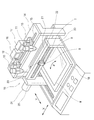
- FIG. 2 is a schematic diagram showing a configuration of a scribing device for a thin-film solar cell according to an embodiment of the present invention.
- the scribing device for a thin-film solar cell according to the present embodiment includes a table 18 that can move in a substantially horizontal direction (Y direction) and that can rotate 90 degrees and an angle ⁇ . I have.
- a bridge 19 composed of support pillars 20 on both sides of the table 18 and a guide bar 21 extending in the X direction is provided so as to straddle the table 18.
- the holder support 23 can move along the guide 22 formed on the guide bar 21, and moves in the X direction by the rotation of the motor 24.
- the holder support 23 is provided with a scribe head 7.
- a holder 9 for holding a cutting edge 8 for scribing the thin film surface of the solar cell substrate W placed on the table 18 is provided below the scribe head 7. It is provided.
- the cameras 10 and 11 are placed on the pedestals 12 and 13 that can move in the X direction and the Y direction.
- the bases 12 and 13 move along a guide 15 provided on a support base 14 extending in the X direction.
- the cameras 10 and 11 can be moved up and down by manual operation, and the focus of imaging can be adjusted. Images captured by the cameras 10 and 11 are displayed on the monitors 16 and 17.
- An alignment mark for specifying the position is described on the surface of the solar cell substrate W placed on the table 18, and the position of the solar cell substrate W is captured by imaging the alignment mark with the cameras 10 and 11. Adjust. Specifically, the alignment marks on the surface of the solar cell substrate W placed on the table 18 are imaged by the cameras 10 and 11, and the position of the alignment mark is specified. Based on the position of the specified alignment mark, a direction shift at the time of placing the solar cell substrate W is detected, and the table 18 is corrected by rotating it by a predetermined angle ⁇ .
- the scribe head 7 is lowered and moved in the X direction with the blade edge 8 pressed against the surface of the solar cell substrate W, so that the surface of the solar cell substrate W is moved. Scribing in the X direction.
- the same operation is performed with the table 18 rotated 90 degrees.
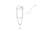
- FIG. 3 is a perspective view showing a configuration of a cutting edge of a conventional scribing device for a thin film solar cell.
- the blade edge 8 ′ has a cylindrical shape and has a tapered shape with a predetermined taper at the tip portion. Further, the tip portion is cut in a direction substantially perpendicular to the cylindrical center line so as to secure a surface area for peeling the thin film of the solar cell substrate W, and the tip portion has a truncated cone shape. That is, the cross-sectional shape is circular with a radius r1 in the cylindrical portion, whereas the cross-sectional shape is circular with a radius r2 smaller than the radius r1 at the tip of the truncated cone-shaped portion.
- the scribing process is performed by moving the scribing head 7 in the Y direction relatively along the planned scribing line while pressing the blade edge 8 ′ having such a shape against the thin film on the surface of the solar cell substrate W.
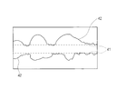
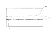
- FIG. 4 is a schematic view showing a scribe line formation state when a conventional cutting edge 8 'is used. As shown in FIG. 4, when the conventional cutting edge 8 ′ is used, although the scribe line 41 indicated by the broken line can be maintained, excessively peeled portions are scattered.
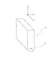
- FIG. 5 is a perspective view showing the configuration of the cutting edge 8 of the scribing device for a thin-film solar cell according to the present embodiment.
- the tip 8 of the scribing device 8 has a so-called cylindrical shape at the tip. That is, the cross-sectional shape of the cutting edge 8 on the surface orthogonal to the X direction is a semicircular shape having a radius R at the tip portion, and the scribe head 7 is pressed while pressing the cutting edge 8 against the thin film on the surface of the solar cell substrate W. Scribing is performed by relatively moving in the X direction.
- FIG. 6 is a schematic diagram showing a scribe line formation state when the cutting edge 8 according to the present embodiment is used.
- the scribe line 41 indicated by the broken line can be traced more accurately, and the excessively peeled portion is also significantly reduced.
- the cutting edge 8 has a cylindrical shape, when the cutting edge 8 is pressed against the solar cell substrate W and moved relatively, the pressing force on the thin film on the surface increases from the center of the cutting edge toward the outside of the cutting edge. This is because the pressing force changes smoothly at the boundary where the thin film peels because it gradually decreases. Therefore, unintentional large peeling does not occur at the boundary portion, and the thin film can be peeled along a desired scribe line.
- the line width of the scribe line can be easily adjusted. That is, since the cutting edge 8 has a cylindrical shape, by increasing or decreasing the semicircular radius R which is a cross-sectional shape in a plane orthogonal to the X direction of the cutting edge 8 and by increasing or decreasing the pressing force of the cutting edge 8 A scribe line can be formed with a desired line width.
- the material of the cutting edge 8 of the scribe head 7 may be diamond (single crystal diamond, sintered diamond (PCD), etc.) or a cemented carbide.
- diamond single crystal diamond, sintered diamond (PCD), etc.
- PCD sintered diamond
- cemented carbide When the cutting edge 8 is formed of cemented carbide, it is possible to cause the same peeling with a lower pressing force than when formed with diamond, and the scribe line width can be adjusted widely. .
- the scribing process is executed by moving the scribe head 7 in the X direction.
- the scribe head 7 may be moved in the X direction and the Y direction while the solar cell substrate W is fixed, or only the solar cell substrate W is moved in the X direction and the Y direction without moving the scribe head 7. You may let them.
- the attachment direction of the blade edge 8 may be changed so that the blade edge 8 is relatively moved in the direction of the line where the tip of the cylindrical blade edge 8 contacts the solar cell substrate W.
Landscapes
- Engineering & Computer Science (AREA)
- Mechanical Engineering (AREA)
- Mining & Mineral Resources (AREA)
- Photovoltaic Devices (AREA)
- Processing Of Stones Or Stones Resemblance Materials (AREA)
Abstract
Description
19 ブリッジ
20 支持柱
21 ガイドバー
22 ガイド
23 ホルダ支持体
9 ホルダ
W 太陽電池基板
7 スクライブヘッド
8 刃先
Claims (2)
- 薄膜太陽電池の基板を支持する支持手段と、
前記基板の一方の面のスクライブ予定ラインに沿って、先端に装着されている刃先を押圧するスクライブヘッドと、
前記基板と前記スクライブヘッドとを相対的に移動させる移動手段と
を備え、
前記スクライブヘッドと前記基板とが相対的に移動することで前記基板の一方の面にスクライブラインを形成する薄膜太陽電池のスクライブ装置であって、
前記スクライブヘッドは、前記刃先の先端形状がシリンドリカル形状であり、相対的に移動する移動方向がシリンドリカル形状の中心線方向と略一致するように前記刃先を配設してあることを特徴とする薄膜太陽電池のスクライブ装置。 - 前記スクライブヘッドの少なくとも刃先は、超硬合金からなることを特徴とする請求項1記載の薄膜太陽電池のスクライブ装置。
Priority Applications (5)
| Application Number | Priority Date | Filing Date | Title |
|---|---|---|---|
| EP20090754566 EP2284871B1 (en) | 2008-05-26 | 2009-05-13 | Scribe apparatus for thin film solar cell |
| CN2009801190161A CN102047392A (zh) | 2008-05-26 | 2009-05-13 | 薄膜太阳电池的划线装置 |
| US12/994,649 US20110126688A1 (en) | 2008-05-26 | 2009-05-13 | Scribing apparatus for thin film solar cell |
| JP2010514430A JP5369099B2 (ja) | 2008-05-26 | 2009-05-13 | 薄膜太陽電池のスクライブ装置 |
| KR1020107026295A KR101193929B1 (ko) | 2008-05-26 | 2009-05-13 | 박막 태양전지의 스크라이브 장치 |
Applications Claiming Priority (2)
| Application Number | Priority Date | Filing Date | Title |
|---|---|---|---|
| JP2008-136865 | 2008-05-26 | ||
| JP2008136865 | 2008-05-26 |
Publications (1)
| Publication Number | Publication Date |
|---|---|
| WO2009145058A1 true WO2009145058A1 (ja) | 2009-12-03 |
Family
ID=41376942
Family Applications (1)
| Application Number | Title | Priority Date | Filing Date |
|---|---|---|---|
| PCT/JP2009/058931 Ceased WO2009145058A1 (ja) | 2008-05-26 | 2009-05-13 | 薄膜太陽電池のスクライブ装置 |
Country Status (7)
| Country | Link |
|---|---|
| US (1) | US20110126688A1 (ja) |
| EP (1) | EP2284871B1 (ja) |
| JP (1) | JP5369099B2 (ja) |
| KR (1) | KR101193929B1 (ja) |
| CN (1) | CN102047392A (ja) |
| TW (1) | TWI417260B (ja) |
| WO (1) | WO2009145058A1 (ja) |
Cited By (9)
| Publication number | Priority date | Publication date | Assignee | Title |
|---|---|---|---|---|
| JP2011142236A (ja) * | 2010-01-08 | 2011-07-21 | Mitsuboshi Diamond Industrial Co Ltd | 薄膜太陽電池用の溝加工ツール及びその角度規制構造 |
| JP2011155151A (ja) * | 2010-01-27 | 2011-08-11 | Mitsuboshi Diamond Industrial Co Ltd | 薄膜太陽電池用スクライブ装置 |
| JP2011155150A (ja) * | 2010-01-27 | 2011-08-11 | Mitsuboshi Diamond Industrial Co Ltd | 溝加工ツール及びこれを用いた薄膜太陽電池の溝加工方法 |
| JP2011238672A (ja) * | 2010-05-07 | 2011-11-24 | Mitsuboshi Diamond Industrial Co Ltd | ツールホルダおよびこれを用いたスクライブ装置 |
| JP2012046385A (ja) * | 2010-08-27 | 2012-03-08 | Mitsubishi Chemical Holdings Corp | 光水分解用電極、光水分解用電極の製造方法、および、水分解方法 |
| EP2469586A1 (en) | 2010-12-24 | 2012-06-27 | Mitsuboshi Diamond Industrial Co., Ltd. | Patterning device |
| JP2013042153A (ja) * | 2009-02-24 | 2013-02-28 | Mitsuboshi Diamond Industrial Co Ltd | 集積型薄膜太陽電池の溝加工方法 |
| JP2016213317A (ja) * | 2015-05-08 | 2016-12-15 | 三星ダイヤモンド工業株式会社 | 薄膜太陽電池の加工装置、および、薄膜太陽電池の加工方法 |
| JP2016213258A (ja) * | 2015-04-30 | 2016-12-15 | 三星ダイヤモンド工業株式会社 | 薄膜太陽電池の加工装置、および、薄膜太陽電池の加工方法 |
Families Citing this family (2)
| Publication number | Priority date | Publication date | Assignee | Title |
|---|---|---|---|---|
| CN102593256B (zh) * | 2012-03-02 | 2014-07-09 | 江苏宇天港玻新材料有限公司 | 一体化cigs薄膜太阳能电池生产设备及其生产方法 |
| CN106206858A (zh) * | 2016-09-05 | 2016-12-07 | 北京四方创能光电科技有限公司 | 一种薄膜太阳能电池i‑v测试前制作多个子电池的划线装置 |
Citations (6)
| Publication number | Priority date | Publication date | Assignee | Title |
|---|---|---|---|---|
| US4057184A (en) * | 1975-09-19 | 1977-11-08 | Ppg Industries, Inc. | Method of scoring glass using a scoring wheel having an arcuate scoring surface |
| JPS6316439U (ja) * | 1986-07-18 | 1988-02-03 | Sanyo Electric Co | |
| JP2002094089A (ja) | 2000-09-11 | 2002-03-29 | Honda Motor Co Ltd | 化合物薄膜太陽電池の製造方法 |
| WO2003040049A1 (fr) * | 2001-11-08 | 2003-05-15 | Sharp Kabushiki Kaisha | Procede et dispositif destines a diviser un substrat de verre, panneau a cristaux liquides et dispositif de fabrication de panneau a cristaux liquides |
| JP2004115356A (ja) | 2002-09-26 | 2004-04-15 | Honda Motor Co Ltd | メカニカルスクライブ装置 |
| JP2007145681A (ja) * | 2005-11-30 | 2007-06-14 | Optrex Corp | 切断刃および切断方法 |
Family Cites Families (12)
| Publication number | Priority date | Publication date | Assignee | Title |
|---|---|---|---|---|
| US3902042A (en) * | 1973-02-21 | 1975-08-26 | Adolph E Goldfarb | Electrically heated tool for cutting designs in a surface |
| US4224854A (en) * | 1978-09-01 | 1980-09-30 | Malacheski Joseph J | Sheet cutting and scoring device and method |
| GB8301710D0 (en) * | 1983-01-21 | 1983-02-23 | Protocol Eng Ltd | Production of lines of separation in sheet & c member |
| DE4135573A1 (de) * | 1990-11-28 | 1992-06-04 | Fein C & E | Verfahren und vorrichtung zum einbringen von oberflaechenkanaelen in plattenmaterial aus weichem werkstoff und verwendung einer vorrichtung |
| US5647265A (en) * | 1993-06-30 | 1997-07-15 | The United States Of America As Represented By The Secretary Of The Navy | Tool and system for machining a round strand |
| EP0786347B1 (en) * | 1995-12-26 | 2003-05-14 | Canon Kabushiki Kaisha | A method for manufacturing a liquid jet recording head, a liquid jet recording head manufactured by such method, and a liquid jet recording apparatus having such head mounted thereon |
| EP0841131A1 (de) * | 1996-11-07 | 1998-05-13 | Bullmer Spezialmaschinen GmbH | Schneidvorrichtung mit Hubregelung |
| JP2000315809A (ja) * | 1999-03-04 | 2000-11-14 | Matsushita Electric Ind Co Ltd | 集積型薄膜太陽電池の製造方法およびパターニング装置 |
| WO2002022296A2 (en) * | 2000-09-11 | 2002-03-21 | Allison Advanced Development Company | Mechanically grooved sheet and method of manufacture |
| JP4885111B2 (ja) * | 2001-11-08 | 2012-02-29 | シャープ株式会社 | 液晶パネル及び液晶パネル製造装置 |
| CN101232982B (zh) * | 2005-05-30 | 2012-03-21 | 三星钻石工业株式会社 | 脆性材料基板分割装置及分割方法 |
| GB2439962B (en) * | 2006-06-14 | 2008-09-24 | Exitech Ltd | Process and apparatus for laser scribing |
-
2009
- 2009-05-13 KR KR1020107026295A patent/KR101193929B1/ko not_active Expired - Fee Related
- 2009-05-13 US US12/994,649 patent/US20110126688A1/en not_active Abandoned
- 2009-05-13 JP JP2010514430A patent/JP5369099B2/ja not_active Expired - Fee Related
- 2009-05-13 EP EP20090754566 patent/EP2284871B1/en not_active Not-in-force
- 2009-05-13 WO PCT/JP2009/058931 patent/WO2009145058A1/ja not_active Ceased
- 2009-05-13 CN CN2009801190161A patent/CN102047392A/zh active Pending
- 2009-05-14 TW TW98115986A patent/TWI417260B/zh not_active IP Right Cessation
Patent Citations (6)
| Publication number | Priority date | Publication date | Assignee | Title |
|---|---|---|---|---|
| US4057184A (en) * | 1975-09-19 | 1977-11-08 | Ppg Industries, Inc. | Method of scoring glass using a scoring wheel having an arcuate scoring surface |
| JPS6316439U (ja) * | 1986-07-18 | 1988-02-03 | Sanyo Electric Co | |
| JP2002094089A (ja) | 2000-09-11 | 2002-03-29 | Honda Motor Co Ltd | 化合物薄膜太陽電池の製造方法 |
| WO2003040049A1 (fr) * | 2001-11-08 | 2003-05-15 | Sharp Kabushiki Kaisha | Procede et dispositif destines a diviser un substrat de verre, panneau a cristaux liquides et dispositif de fabrication de panneau a cristaux liquides |
| JP2004115356A (ja) | 2002-09-26 | 2004-04-15 | Honda Motor Co Ltd | メカニカルスクライブ装置 |
| JP2007145681A (ja) * | 2005-11-30 | 2007-06-14 | Optrex Corp | 切断刃および切断方法 |
Non-Patent Citations (1)
| Title |
|---|
| See also references of EP2284871A4 |
Cited By (12)
| Publication number | Priority date | Publication date | Assignee | Title |
|---|---|---|---|---|
| JP2013042153A (ja) * | 2009-02-24 | 2013-02-28 | Mitsuboshi Diamond Industrial Co Ltd | 集積型薄膜太陽電池の溝加工方法 |
| JP5269183B2 (ja) * | 2009-02-24 | 2013-08-21 | 三星ダイヤモンド工業株式会社 | 溝加工ツールおよびこれを用いた薄膜太陽電池のスクライブ装置 |
| JP2011142236A (ja) * | 2010-01-08 | 2011-07-21 | Mitsuboshi Diamond Industrial Co Ltd | 薄膜太陽電池用の溝加工ツール及びその角度規制構造 |
| JP2011155151A (ja) * | 2010-01-27 | 2011-08-11 | Mitsuboshi Diamond Industrial Co Ltd | 薄膜太陽電池用スクライブ装置 |
| JP2011155150A (ja) * | 2010-01-27 | 2011-08-11 | Mitsuboshi Diamond Industrial Co Ltd | 溝加工ツール及びこれを用いた薄膜太陽電池の溝加工方法 |
| KR101251896B1 (ko) * | 2010-01-27 | 2013-04-08 | 미쓰보시 다이야몬도 고교 가부시키가이샤 | 박막 태양 전지용 스크라이브 장치 |
| JP2011238672A (ja) * | 2010-05-07 | 2011-11-24 | Mitsuboshi Diamond Industrial Co Ltd | ツールホルダおよびこれを用いたスクライブ装置 |
| JP2012046385A (ja) * | 2010-08-27 | 2012-03-08 | Mitsubishi Chemical Holdings Corp | 光水分解用電極、光水分解用電極の製造方法、および、水分解方法 |
| EP2469586A1 (en) | 2010-12-24 | 2012-06-27 | Mitsuboshi Diamond Industrial Co., Ltd. | Patterning device |
| JP2012146948A (ja) * | 2010-12-24 | 2012-08-02 | Mitsuboshi Diamond Industrial Co Ltd | パターニング装置 |
| JP2016213258A (ja) * | 2015-04-30 | 2016-12-15 | 三星ダイヤモンド工業株式会社 | 薄膜太陽電池の加工装置、および、薄膜太陽電池の加工方法 |
| JP2016213317A (ja) * | 2015-05-08 | 2016-12-15 | 三星ダイヤモンド工業株式会社 | 薄膜太陽電池の加工装置、および、薄膜太陽電池の加工方法 |
Also Published As
| Publication number | Publication date |
|---|---|
| TWI417260B (zh) | 2013-12-01 |
| TW201000414A (en) | 2010-01-01 |
| KR101193929B1 (ko) | 2012-10-23 |
| EP2284871A1 (en) | 2011-02-16 |
| JPWO2009145058A1 (ja) | 2011-10-06 |
| JP5369099B2 (ja) | 2013-12-18 |
| US20110126688A1 (en) | 2011-06-02 |
| CN102047392A (zh) | 2011-05-04 |
| EP2284871A4 (en) | 2011-05-11 |
| KR20100134784A (ko) | 2010-12-23 |
| EP2284871B1 (en) | 2012-10-10 |
Similar Documents
| Publication | Publication Date | Title |
|---|---|---|
| JP5369099B2 (ja) | 薄膜太陽電池のスクライブ装置 | |
| JP5351998B2 (ja) | 集積型薄膜太陽電池の溝加工方法 | |
| JP5308892B2 (ja) | 集積型薄膜太陽電池の製造装置 | |
| JP2004115356A (ja) | メカニカルスクライブ装置 | |
| WO2010103947A1 (ja) | 薄膜太陽電池用の溝加工ツール | |
| JP5357580B2 (ja) | 溝加工ツールおよびこれを用いた薄膜太陽電池の溝加工方法 | |
| KR101512705B1 (ko) | 홈 가공 툴 및 이것을 이용한 박막 태양 전지의 홈 가공 방법 그리고 홈 가공 장치 | |
| JP2015126205A (ja) | 溝加工ツール並びにこの溝加工ツールを取り付けたスクライブ装置 | |
| HK1153571A (en) | Scribe apparatus for thin film solar cell | |
| JP5369011B2 (ja) | 溝加工ツール及びこれを用いた薄膜太陽電池の溝加工方法 | |
| JP2020107798A (ja) | 溝加工ツールおよびこれを用いた薄膜太陽電池の溝加工方法ならびに溝加工装置 | |
| JP2020107799A (ja) | 溝加工ツールおよびこれを用いた薄膜太陽電池の溝加工方法ならびに溝加工装置 | |
| JP2020107795A (ja) | 溝加工ツールおよびこれを用いた薄膜太陽電池の溝加工方法ならびに溝加工装置 | |
| JP2020107796A (ja) | 溝加工ツールおよびこれを用いた薄膜太陽電池の溝加工方法ならびに溝加工装置 | |
| JP2020107800A (ja) | 溝加工ツールおよびこれを用いた薄膜太陽電池の溝加工方法ならびに溝加工装置 | |
| JP2020107797A (ja) | 溝加工ツールおよびこれを用いた薄膜太陽電池の溝加工方法ならびに溝加工装置 |
Legal Events
| Date | Code | Title | Description |
|---|---|---|---|
| WWE | Wipo information: entry into national phase |
Ref document number: 200980119016.1 Country of ref document: CN |
|
| 121 | Ep: the epo has been informed by wipo that ep was designated in this application |
Ref document number: 09754566 Country of ref document: EP Kind code of ref document: A1 |
|
| WWE | Wipo information: entry into national phase |
Ref document number: 2010514430 Country of ref document: JP |
|
| WWE | Wipo information: entry into national phase |
Ref document number: 2009754566 Country of ref document: EP |
|
| ENP | Entry into the national phase |
Ref document number: 20107026295 Country of ref document: KR Kind code of ref document: A |
|
| NENP | Non-entry into the national phase |
Ref country code: DE |
|
| WWE | Wipo information: entry into national phase |
Ref document number: 12994649 Country of ref document: US |