WO2009145179A1 - 多層フレキシブルプリント配線板の接着層形成用の樹脂組成物 - Google Patents
多層フレキシブルプリント配線板の接着層形成用の樹脂組成物 Download PDFInfo
- Publication number
- WO2009145179A1 WO2009145179A1 PCT/JP2009/059591 JP2009059591W WO2009145179A1 WO 2009145179 A1 WO2009145179 A1 WO 2009145179A1 JP 2009059591 W JP2009059591 W JP 2009059591W WO 2009145179 A1 WO2009145179 A1 WO 2009145179A1
- Authority
- WO
- WIPO (PCT)
- Prior art keywords
- resin
- component
- weight
- wiring board
- flexible printed
- Prior art date
- Legal status (The legal status is an assumption and is not a legal conclusion. Google has not performed a legal analysis and makes no representation as to the accuracy of the status listed.)
- Ceased
Links
Classifications
-
- C—CHEMISTRY; METALLURGY
- C09—DYES; PAINTS; POLISHES; NATURAL RESINS; ADHESIVES; COMPOSITIONS NOT OTHERWISE PROVIDED FOR; APPLICATIONS OF MATERIALS NOT OTHERWISE PROVIDED FOR
- C09J—ADHESIVES; NON-MECHANICAL ASPECTS OF ADHESIVE PROCESSES IN GENERAL; ADHESIVE PROCESSES NOT PROVIDED FOR ELSEWHERE; USE OF MATERIALS AS ADHESIVES
- C09J163/00—Adhesives based on epoxy resins; Adhesives based on derivatives of epoxy resins
-
- C—CHEMISTRY; METALLURGY
- C08—ORGANIC MACROMOLECULAR COMPOUNDS; THEIR PREPARATION OR CHEMICAL WORKING-UP; COMPOSITIONS BASED THEREON
- C08G—MACROMOLECULAR COMPOUNDS OBTAINED OTHERWISE THAN BY REACTIONS ONLY INVOLVING UNSATURATED CARBON-TO-CARBON BONDS
- C08G73/00—Macromolecular compounds obtained by reactions forming a linkage containing nitrogen with or without oxygen or carbon in the main chain of the macromolecule, not provided for in groups C08G12/00 - C08G71/00
- C08G73/06—Polycondensates having nitrogen-containing heterocyclic rings in the main chain of the macromolecule
- C08G73/10—Polyimides; Polyester-imides; Polyamide-imides; Polyamide acids or similar polyimide precursors
- C08G73/14—Polyamide-imides
-
- C—CHEMISTRY; METALLURGY
- C09—DYES; PAINTS; POLISHES; NATURAL RESINS; ADHESIVES; COMPOSITIONS NOT OTHERWISE PROVIDED FOR; APPLICATIONS OF MATERIALS NOT OTHERWISE PROVIDED FOR
- C09J—ADHESIVES; NON-MECHANICAL ASPECTS OF ADHESIVE PROCESSES IN GENERAL; ADHESIVE PROCESSES NOT PROVIDED FOR ELSEWHERE; USE OF MATERIALS AS ADHESIVES
- C09J179/00—Adhesives based on macromolecular compounds obtained by reactions forming in the main chain of the macromolecule a linkage containing nitrogen, with or without oxygen, or carbon only, not provided for in groups C09J161/00 - C09J177/00
- C09J179/04—Polycondensates having nitrogen-containing heterocyclic rings in the main chain; Polyhydrazides; Polyamide acids or similar polyimide precursors
- C09J179/08—Polyimides; Polyester-imides; Polyamide-imides; Polyamide acids or similar polyimide precursors
-
- H—ELECTRICITY
- H05—ELECTRIC TECHNIQUES NOT OTHERWISE PROVIDED FOR
- H05K—PRINTED CIRCUITS; CASINGS OR CONSTRUCTIONAL DETAILS OF ELECTRIC APPARATUS; MANUFACTURE OF ASSEMBLAGES OF ELECTRICAL COMPONENTS
- H05K3/00—Apparatus or processes for manufacturing printed circuits
- H05K3/46—Manufacturing multilayer circuits
- H05K3/4611—Manufacturing multilayer circuits by laminating two or more circuit boards
- H05K3/4626—Manufacturing multilayer circuits by laminating two or more circuit boards characterised by the insulating layers or materials
- H05K3/4635—Manufacturing multilayer circuits by laminating two or more circuit boards characterised by the insulating layers or materials laminating flexible circuit boards using additional insulating adhesive materials between the boards
-
- H—ELECTRICITY
- H05—ELECTRIC TECHNIQUES NOT OTHERWISE PROVIDED FOR
- H05K—PRINTED CIRCUITS; CASINGS OR CONSTRUCTIONAL DETAILS OF ELECTRIC APPARATUS; MANUFACTURE OF ASSEMBLAGES OF ELECTRICAL COMPONENTS
- H05K3/00—Apparatus or processes for manufacturing printed circuits
- H05K3/46—Manufacturing multilayer circuits
- H05K3/4644—Manufacturing multilayer circuits by building the multilayer layer by layer, i.e. build-up multilayer circuits
- H05K3/4652—Adding a circuit layer by laminating a metal foil or a preformed metal foil pattern
- H05K3/4655—Adding a circuit layer by laminating a metal foil or a preformed metal foil pattern by using a laminate characterized by the insulating layer
-
- C—CHEMISTRY; METALLURGY
- C08—ORGANIC MACROMOLECULAR COMPOUNDS; THEIR PREPARATION OR CHEMICAL WORKING-UP; COMPOSITIONS BASED THEREON
- C08L—COMPOSITIONS OF MACROMOLECULAR COMPOUNDS
- C08L2203/00—Applications
- C08L2203/20—Applications use in electrical or conductive gadgets
-
- C—CHEMISTRY; METALLURGY
- C08—ORGANIC MACROMOLECULAR COMPOUNDS; THEIR PREPARATION OR CHEMICAL WORKING-UP; COMPOSITIONS BASED THEREON
- C08L—COMPOSITIONS OF MACROMOLECULAR COMPOUNDS
- C08L2666/00—Composition of polymers characterized by a further compound in the blend, being organic macromolecular compounds, natural resins, waxes or and bituminous materials, non-macromolecular organic substances, inorganic substances or characterized by their function in the composition
- C08L2666/02—Organic macromolecular compounds, natural resins, waxes or and bituminous materials
- C08L2666/14—Macromolecular compounds according to C08L59/00 - C08L87/00; Derivatives thereof
- C08L2666/20—Macromolecular compounds having nitrogen in the main chain according to C08L75/00 - C08L79/00; Derivatives thereof
-
- C—CHEMISTRY; METALLURGY
- C08—ORGANIC MACROMOLECULAR COMPOUNDS; THEIR PREPARATION OR CHEMICAL WORKING-UP; COMPOSITIONS BASED THEREON
- C08L—COMPOSITIONS OF MACROMOLECULAR COMPOUNDS
- C08L2666/00—Composition of polymers characterized by a further compound in the blend, being organic macromolecular compounds, natural resins, waxes or and bituminous materials, non-macromolecular organic substances, inorganic substances or characterized by their function in the composition
- C08L2666/02—Organic macromolecular compounds, natural resins, waxes or and bituminous materials
- C08L2666/14—Macromolecular compounds according to C08L59/00 - C08L87/00; Derivatives thereof
- C08L2666/22—Macromolecular compounds not provided for in C08L2666/16 - C08L2666/20
-
- C—CHEMISTRY; METALLURGY
- C08—ORGANIC MACROMOLECULAR COMPOUNDS; THEIR PREPARATION OR CHEMICAL WORKING-UP; COMPOSITIONS BASED THEREON
- C08L—COMPOSITIONS OF MACROMOLECULAR COMPOUNDS
- C08L63/00—Compositions of epoxy resins; Compositions of derivatives of epoxy resins
-
- C—CHEMISTRY; METALLURGY
- C08—ORGANIC MACROMOLECULAR COMPOUNDS; THEIR PREPARATION OR CHEMICAL WORKING-UP; COMPOSITIONS BASED THEREON
- C08L—COMPOSITIONS OF MACROMOLECULAR COMPOUNDS
- C08L79/00—Compositions of macromolecular compounds obtained by reactions forming in the main chain of the macromolecule a linkage containing nitrogen with or without oxygen or carbon only, not provided for in groups C08L61/00 - C08L77/00
- C08L79/04—Polycondensates having nitrogen-containing heterocyclic rings in the main chain; Polyhydrazides; Polyamide acids or similar polyimide precursors
- C08L79/08—Polyimides; Polyester-imides; Polyamide-imides; Polyamide acids or similar polyimide precursors
-
- H—ELECTRICITY
- H05—ELECTRIC TECHNIQUES NOT OTHERWISE PROVIDED FOR
- H05K—PRINTED CIRCUITS; CASINGS OR CONSTRUCTIONAL DETAILS OF ELECTRIC APPARATUS; MANUFACTURE OF ASSEMBLAGES OF ELECTRICAL COMPONENTS
- H05K1/00—Printed circuits
- H05K1/02—Details
- H05K1/03—Use of materials for the substrate
- H05K1/0393—Flexible materials
-
- H—ELECTRICITY
- H05—ELECTRIC TECHNIQUES NOT OTHERWISE PROVIDED FOR
- H05K—PRINTED CIRCUITS; CASINGS OR CONSTRUCTIONAL DETAILS OF ELECTRIC APPARATUS; MANUFACTURE OF ASSEMBLAGES OF ELECTRICAL COMPONENTS
- H05K2201/00—Indexing scheme relating to printed circuits covered by H05K1/00
- H05K2201/01—Dielectrics
- H05K2201/0104—Properties and characteristics in general
- H05K2201/012—Flame-retardant; Preventing of inflammation
-
- H—ELECTRICITY
- H05—ELECTRIC TECHNIQUES NOT OTHERWISE PROVIDED FOR
- H05K—PRINTED CIRCUITS; CASINGS OR CONSTRUCTIONAL DETAILS OF ELECTRIC APPARATUS; MANUFACTURE OF ASSEMBLAGES OF ELECTRICAL COMPONENTS
- H05K2201/00—Indexing scheme relating to printed circuits covered by H05K1/00
- H05K2201/01—Dielectrics
- H05K2201/0137—Materials
- H05K2201/0154—Polyimide
-
- H—ELECTRICITY
- H05—ELECTRIC TECHNIQUES NOT OTHERWISE PROVIDED FOR
- H05K—PRINTED CIRCUITS; CASINGS OR CONSTRUCTIONAL DETAILS OF ELECTRIC APPARATUS; MANUFACTURE OF ASSEMBLAGES OF ELECTRICAL COMPONENTS
- H05K2201/00—Indexing scheme relating to printed circuits covered by H05K1/00
- H05K2201/03—Conductive materials
- H05K2201/0332—Structure of the conductor
- H05K2201/0335—Layered conductors or foils
- H05K2201/0358—Resin coated copper [RCC]
-
- H—ELECTRICITY
- H05—ELECTRIC TECHNIQUES NOT OTHERWISE PROVIDED FOR
- H05K—PRINTED CIRCUITS; CASINGS OR CONSTRUCTIONAL DETAILS OF ELECTRIC APPARATUS; MANUFACTURE OF ASSEMBLAGES OF ELECTRICAL COMPONENTS
- H05K3/00—Apparatus or processes for manufacturing printed circuits
- H05K3/38—Improvement of the adhesion between the insulating substrate and the metal
- H05K3/386—Improvement of the adhesion between the insulating substrate and the metal by the use of an organic polymeric bonding layer, e.g. adhesive
-
- H—ELECTRICITY
- H05—ELECTRIC TECHNIQUES NOT OTHERWISE PROVIDED FOR
- H05K—PRINTED CIRCUITS; CASINGS OR CONSTRUCTIONAL DETAILS OF ELECTRIC APPARATUS; MANUFACTURE OF ASSEMBLAGES OF ELECTRICAL COMPONENTS
- H05K3/00—Apparatus or processes for manufacturing printed circuits
- H05K3/46—Manufacturing multilayer circuits
- H05K3/4644—Manufacturing multilayer circuits by building the multilayer layer by layer, i.e. build-up multilayer circuits
- H05K3/4652—Adding a circuit layer by laminating a metal foil or a preformed metal foil pattern
Definitions
- the invention according to the present application includes a resin composition for forming an adhesive layer of a multilayer flexible printed wiring board, a resin varnish obtained from the resin composition, a resin-coated copper foil in which a resin layer is formed with the resin varnish, and the resin-coated copper.
- the present invention relates to a foil manufacturing method and a multilayer flexible printed wiring board.
- the printed wiring board is roughly classified into a plate-like rigid rigid board and a flexible printed wiring board having bendability.
- the rigid wiring board can be easily multi-layered, and the size of the substrate has been reduced by increasing the number of layers early.
- the flexible printed wiring board is also required to be miniaturized, as described in Patent Document 1, multilayering similar to the rigid printed wiring board is required.
- the multilayer flexible printed wiring board disclosed in Patent Document 1 is an inner layer positioned on a laminated boundary surface by bonding an inner layer substrate on which a circuit pattern is formed and another inner layer substrate or a metal foil via a bonding sheet.
- a bonding sheet is used for the purpose of forming a resin layer as a buffer layer for flattening unevenness due to a circuit pattern.
- This bonding sheet has been known to be made of a resin mainly composed of an epoxy resin or an acrylic resin.
- the resin layer formed using this bonding sheet has a problem that it is not rigid and has low mechanical strength and is brittle.
- thermosetting adhesive sheet for flexible printed wiring boards that is less likely to cause powdering of the adhesive resin during processing and is easy to mold.
- This thermosetting adhesive sheet for flexible printed wiring boards comprises a base material which is a woven fabric or a non-woven fabric and an adhesive resin composition, and the adhesive resin composition comprises (A) two or more epoxy groups in one molecule.
- C epoxy It contains a resin curing agent (however, the weight ratio of the epoxy resin (A) to the thermoplastic resin (B) is 20:80 to 70:30).
- Patent Document 3 discloses a multilayer rigid flexible wiring board in which a first flexible substrate is used as a core material, and a rigid substrate is laminated on the core material via a coverlay, and an adhesive function is provided instead of the coverlay.
- a multilayer rigid flexible wiring board characterized by using a flexible insulating material is disclosed, and the use of a resin film with an adhesive for the flexible insulating material is disclosed.
- the multilayer rigid flexible wiring board disclosed in Patent Document 3 is manufactured by combining a raw material for manufacturing a rigid printed wiring board and a raw material for manufacturing a flexible printed wiring board, and using the flexible printed wiring board as a core material, A flexible part and a rigid part are formed integrally. For example, an example is also shown in FIG. At this time, it is necessary to protect the conductor circuits formed on both surfaces of the flexible printed wiring board used for the core material. In such a case, the surface of the core material is usually covered with a cover lay film, but in the invention disclosed in Patent Document 3, the cover lay film can be omitted by covering with the above-described resin layer.
- a halogen-free epoxy resin composition or the like as disclosed in Patent Document 4 as a flexible resin having flexibility.
- the epoxy resin composition at this time is imparted with flame retardancy by the phosphorus-containing compound, and is given flexibility by adding a crosslinked rubber, a polyvinyl acetal resin, or the like.
- acrylonitrile butadiene rubber (NBR), SBR, BR, IR, EPM, EPDM, CR, butyl rubber, urethane rubber, silicone rubber, polysulfide rubber, hydrogenated nitrile rubber are elastomer components.
- Polyether special rubber, fluoro rubber, tetrafluoroethylene propylene rubber, acrylic rubber, epichlorohydrin rubber, propylene oxide rubber, ethylene vinyl acetate copolymer, ethylene acrylic rubber and the like are disclosed.
- the bonding sheet disclosed in Patent Document 1 is mainly composed of an epoxy resin or an acrylic resin, and the resin layer formed using this bonding sheet is not rigid and has a low mechanical strength and is brittle. Therefore, it has been difficult to use in a multilayer flexible printed wiring board that requires repeated bending operations. Further, when a bonding sheet is used, it is necessary to once form a resin sheet, so that there is a limit to reducing the thickness. As a result, as long as the bonding sheet is used, there is a limit to reducing the thickness of the multilayer flexible printed wiring board.
- Patent Document 2 Even if the resin composition disclosed in Patent Document 2 is used for forming a resin layer that does not include a skeleton material such as a woven fabric or a non-woven fabric, when a thermoplastic resin such as a phenoxy resin is used in combination with an epoxy resin, the resin layer after curing lacks flexibility, cannot follow the expansion / contraction behavior with other insulating layer constituting materials when multilayered, and causes problems such as cracks in the cured resin layer.
- a resin film with an adhesive disclosed in Patent Document 3 and a halogen-free epoxy resin composition disclosed in Patent Document 4 are used as conventional multilayer flexible printed wiring boards as described in Patent Document 1 and Patent Document 2. Even if it is considered to be diverted to the resin layer forming material, the cured adhesive layer is hard and brittle, so lacks flexibility, and expands and contracts with other insulating layer constituent materials when multilayered Cannot be followed, and a defect such as a crack occurring in the cured resin layer occurs.
- the inventors of the present invention as a result of earnest research, constituted the resin layer of the resin-coated copper foil with the resin composition described below, and by using this resin-coated copper foil for the production of a multilayer flexible printed wiring board, The inventor came up with the idea that the above problems could be solved. Hereinafter, the present invention will be described. *
- Resin composition for forming an adhesive layer of a multilayer flexible printed wiring board is obtained by laminating a printed wiring board for an outer layer on the surface of an inner flexible printed wiring board.
- a resin composition used for forming an adhesive layer for the above-described purpose comprising the following components A to E.
- Component A An epoxy resin having one or more selected from the group consisting of a bisphenol A type epoxy resin, a bisphenol F type epoxy resin, and a bisphenol AD type epoxy resin that have an epoxy equivalent of 200 or less and are liquid at room temperature.
- B component High heat-resistant epoxy resin.
- Component C Flame retardant epoxy resin containing phosphorus.
- Component D A rubber-modified polyamideimide resin modified with a liquid rubber component having a property of being soluble in a solvent having a boiling point in the range of 50 ° C. to 200 ° C.
- Component E A resin curing agent comprising one or more of a biphenyl type phenol resin and a phenol aralkyl type phenol resin.
- Resin varnish for forming an adhesive layer of a multilayer flexible printed wiring board according to the present invention is obtained by adding a solvent to the resin composition described above to form a resin solid A semi-cured resin film having a resin flow in the range of 1% to 30% when the amount is prepared in the range of 30% to 70% by weight and measured according to MIL-P-13949G in the MIL standard is formed. It is characterized by what is possible.
- Resin-coated copper foil for manufacturing a multilayer flexible printed wiring board according to the present invention is provided with a resin having a semi-cured resin layer on the surface of the copper foil. It is copper foil, The said resin layer is formed using the resin composition for the contact bonding layer formation of the above-mentioned multilayer flexible printed wiring board, It is characterized by the above-mentioned.
- the resin-coated copper foil according to the present invention is a polyimide resin, a polyamide resin, a polyether sulfone resin, a phenoxy resin, an aramid resin, a polyvinyl acetal resin, or between the copper foil and the semi-cured resin layer. It is also possible to improve the flexibility by forming an auxiliary resin layer made of two or more kinds of mixed resins before forming the semi-cured resin layer.
- the manufacturing method of resin-coated copper foil for manufacturing a multilayer flexible printed wiring board according to the present invention is a resin used for forming a resin layer in the following steps a and b.
- a varnish is prepared, the resin varnish is applied to the surface of a copper foil, and dried to form a resin-coated copper foil as a semi-cured resin film having a thickness of 10 ⁇ m to 50 ⁇ m.
- Step a 3 to 20 parts by weight of component A, 3 to 30 parts by weight of component B, 5 to 50 parts by weight of component C, 10 to 40 parts by weight of component D and 10 to 40 parts by weight of component E
- each component is mixed to contain a C component-derived phosphorus atom in a range of 0.5% by weight to 3.0% by weight.
- the resin composition is made.
- Step b The resin composition is dissolved using an organic solvent to obtain a resin varnish having a resin solid content of 30 wt% to 70 wt%.
- Multilayer flexible printed wiring board according to the present invention The multilayer flexible printed wiring board according to the present invention is obtained by using the above-described resin composition for forming an adhesive layer of a multilayer flexible printed wiring board. .
- the resin composition for forming the adhesive layer of the multilayer flexible printed wiring board according to the present invention can be processed into a resin varnish and used as a resin layer constituting the insulating layer in the manufacturing process of the multilayer flexible printed wiring board. Since it becomes rich in sufficient flexibility, it is possible to provide a high-quality multilayer flexible printed wiring board. Moreover, the resin-coated copper foil according to the present invention uses the resin composition and the resin varnish. And compared to the case where a resin sheet such as a bonding sheet is used, the resin layer can be made thinner by using it in the form of this resin-coated copper foil, and the resin layer cured in the multilayering process has no flexibility. The trouble which arises can also be controlled. Therefore, the thickness of the interlayer insulating layer when manufacturing the multilayer flexible printed wiring board can be reduced, and a high-quality multilayer flexible printed wiring board can be provided.
- the resin composition for forming an adhesive layer of a multilayer flexible printed wiring board according to the present invention is for forming an adhesive layer for bonding an outer printed wiring board to the surface of an inner flexible printed wiring board that is an inner layer core material. It is a resin composition to be used.
- the inner layer flexible printed wiring board a polyimide resin film is used as a substrate, circuits are provided on both surfaces, and conduction between the circuits on both surfaces is secured by means such as via holes as necessary. Then, a new outer conductor layer is provided on both sides or one side of the inner layer flexible printed wiring board via an insulating layer.
- the outer conductor layer located on the outer layer is etched to form an outer layer circuit.
- the outer conductor layer is formed by providing an adhesive layer on both sides or one side of the inner flexible printed wiring board, placing a prepreg thereon, and placing a metal foil such as a copper foil thereon. Then, by hot pressing, a so-called four-layer copper-clad laminate is obtained, and the outer conductor layer is etched to form a multilayer flexible printed wiring board. Also, resin-coated copper foil is placed on both or one side of the inner layer flexible printed wiring board, and hot pressing is performed to form a so-called four-layer copper-clad laminate, and the outer conductor layer is etched to produce a multilayer It becomes a flexible printed wiring board.
- multilayer rigid flexible printed wiring board and the latter as “multilayer flexible printed wiring board”.
- flexible printed wiring board is of the latter concept.
- concept includes a printed wiring board having four or more layers exemplified here.
- the resin layer of the resin-coated copper foil is composed of a resin composition characterized in that each of the components A to E described below is included as a basic constituent component. Hereinafter, each component will be described.
- the component A is an epoxy resin composed of one or more selected from the group consisting of a bisphenol A type epoxy resin, a bisphenol F type epoxy resin, and a bisphenol AD type epoxy resin that have an epoxy equivalent of 200 or less and are liquid at room temperature.
- the bisphenol-based epoxy resin is selectively used because it has good compatibility with the D component (rubber-modified polyamideimide resin) described later, and it is easy to impart appropriate flexibility to the resin film in a semi-cured state. It is.
- the epoxy equivalent exceeds 200, the resin becomes semi-solid at room temperature, and the flexibility in the semi-cured state is decreased, which is not preferable.
- 1 type may be used independently or 2 or more types may be used in mixture.
- This epoxy resin is preferably used in a blending ratio of 3 to 20 parts by weight, based on 100 parts by weight of the resin composition.
- the epoxy resin is less than 3 parts by weight, the thermosetting property is not sufficiently exhibited, and the function as a binder with the inner layer flexible printed wiring board and the adhesiveness with the copper foil as the resin-coated copper foil are sufficient. It becomes difficult to do.
- the amount exceeds 20 parts by weight the viscosity of the resin varnish increases from the balance with other resin components, and when the resin-coated copper foil is produced, the resin film with a uniform thickness is formed on the copper foil surface. Formation becomes difficult.
- a D component rubber-modified polyamideimide resin
- the B component is a so-called “high heat resistant epoxy resin” having a high glass transition point.
- the “high heat-resistant epoxy resin” referred to here is preferably a polyfunctional epoxy resin such as a novolac-type epoxy resin, a cresol novolac-type epoxy resin, a phenol novolac-type epoxy resin, or a naphthalene-type epoxy resin.
- the component B is preferably used in the range of 3 to 30 parts by weight when the resin composition is 100 parts by weight. When the component B is less than 3 parts by weight, the resin composition cannot have a high Tg. On the other hand, when the B component exceeds 30 parts by weight, the cured resin becomes brittle and the flexibility is completely impaired, which is not preferable for flexible printed wiring board applications. More preferably, the B component is used in the range of 10 to 20 parts by weight, so that both high Tg of the resin composition and good flexibility of the cured resin can be stably achieved.
- the C component is a so-called halogen-free flame retardant epoxy resin, and a phosphorus-containing flame retardant epoxy resin is used.
- the phosphorus-containing flame-retardant epoxy resin is a general term for epoxy resins containing phosphorus in an epoxy skeleton. Further, when the phosphorus atom content of the resin composition according to the present application is 100% by weight of the resin composition, the phosphorus atom derived from the component C can be in the range of 0.5% by weight to 3.0% by weight. Any phosphorus-containing flame-retardant epoxy resin can be used.
- a phosphorus-containing flame-retardant epoxy resin that is a 9,10-dihydro-9-oxa-10-phosphaphenanthrene-10-oxide derivative having two or more epoxy groups in the molecule in a semi-cured state. It is preferable because of its excellent resin quality stability and high flame retardant effect.
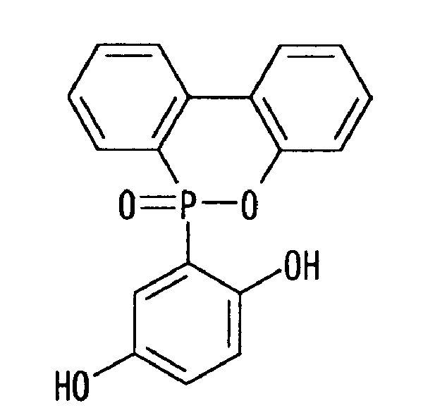
- the structural formula of 9,10-dihydro-9-oxa-10-phosphaphenanthrene-10-oxide is shown in Chemical Formula 1.
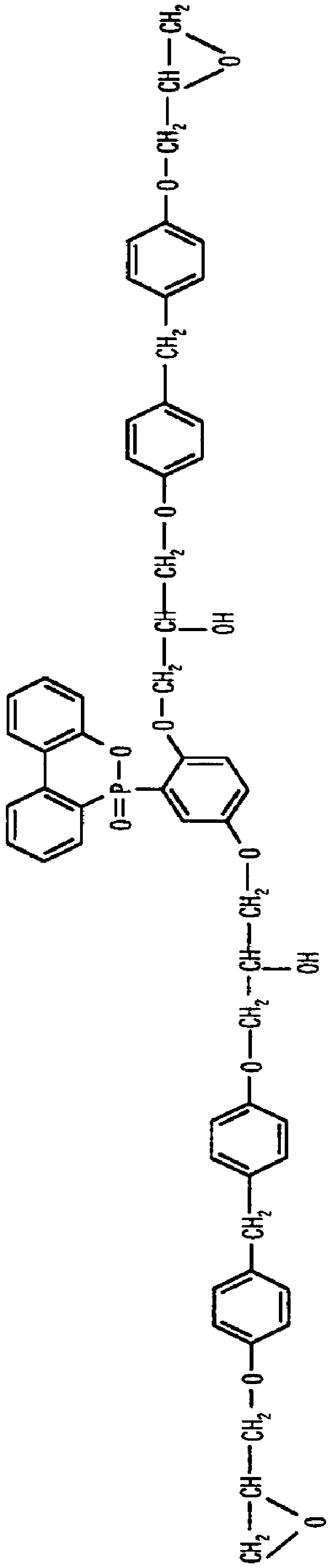
- a specific example of a phosphorus-containing flame-retardant epoxy resin that is a 9,10-dihydro-9-oxa-10-phosphaphenanthrene-10-oxide derivative is the use of a compound having the structural formula shown in Chemical Formula 2. preferable. It is preferable because it is excellent in the stability of the resin quality in a semi-cured state and at the same time has a high flame retardant effect.
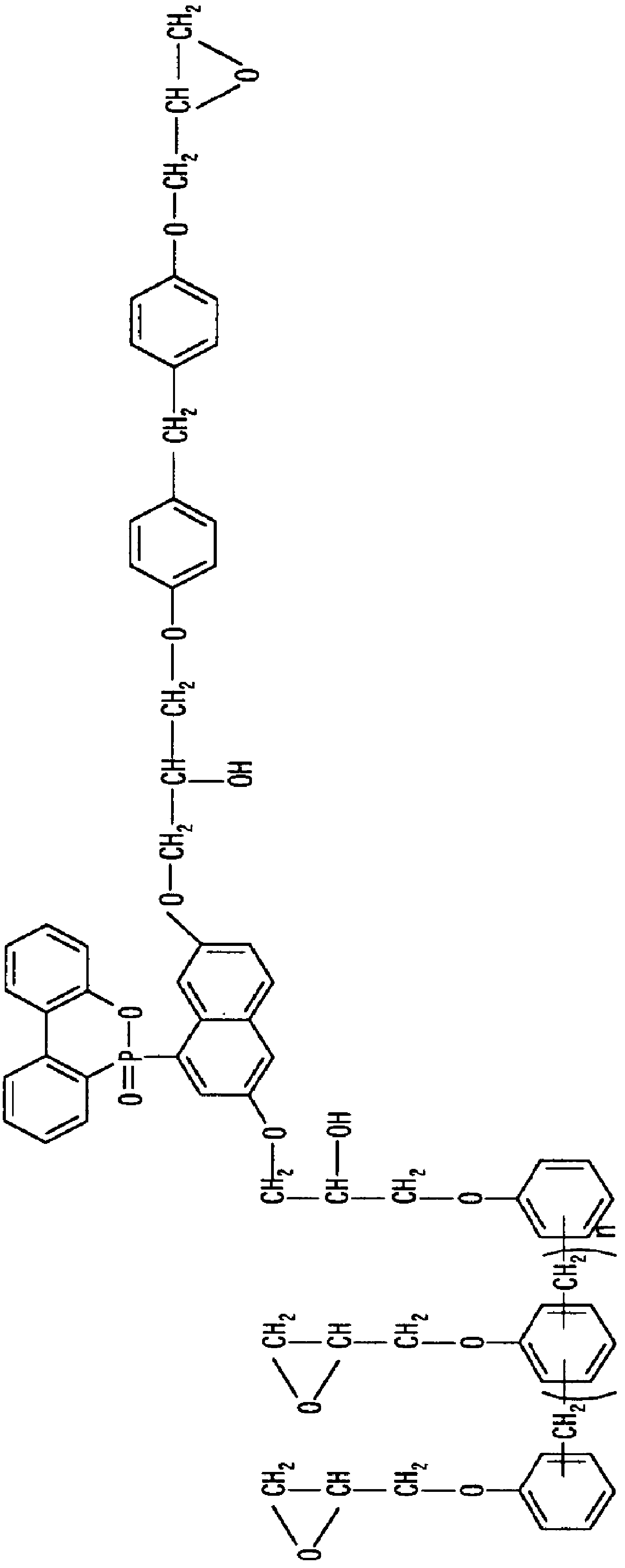
- phosphorus-containing flame retardant epoxy resin of component C a compound having the structural formula shown in Chemical Formula 3 below is also preferable.
- phosphorus-containing flame-retardant epoxy resin shown in Chemical Formula 2 it is preferable because it is excellent in the stability of the resin quality in a semi-cured state and at the same time imparting high flame retardancy.
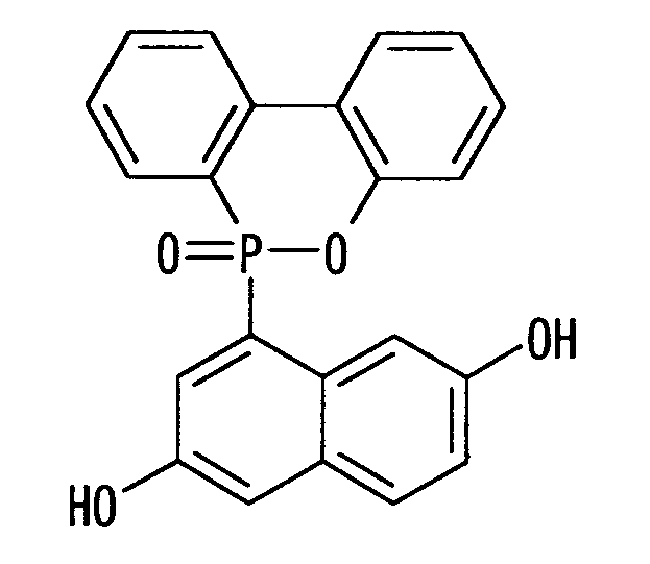
- phosphorus-containing flame retardant epoxy resin of component C a compound having the structural formula shown in Chemical Formula 4 below is also preferable. Like the phosphorus-containing flame retardant epoxy resin shown in Chemical Formula 2 and Chemical Formula 3, it is preferable because it is excellent in the stability of the resin quality in a semi-cured state and at the same time can impart high flame retardancy.
- the epoxy resin obtained as a derivative from 9,10-dihydro-9-oxa-10-phosphaphenanthrene-10-oxide is converted to 9,10-dihydro-9-oxa-10-phosphaphenanthrene-10-oxide.
- an epoxy resin is reacted with the OH group portion to make a phosphorus-containing flame-retardant epoxy. What was made into resin is mentioned.
- the resin composition in the case of using the phosphorus-containing flame-retardant epoxy resin is not limited to two types of phosphorus-containing flame-retardant epoxy resins even if one of the phosphorus-containing flame-retardant epoxy resins as the C component is used alone. May be used in combination.
- the phosphorus atom derived from the C component is 0.5% by weight to 3.0% by weight. It is preferable to add so that it may become this range.
- the phosphorus-containing flame-retardant epoxy resin has different amounts of phosphorus atoms contained in the epoxy skeleton depending on the type.
- the component C is usually used in the range of 5 to 50 parts by weight when the resin composition is 100 parts by weight. In the case where the C component is less than 5 parts by weight, it is difficult to make the phosphorus atom derived from the C component 0.5% by weight or more in consideration of the blending ratio of other resin components, and to obtain flame retardancy. I can't. On the other hand, even if the C component exceeds 50 parts by weight, the effect of improving flame retardancy is saturated, and at the same time, the cured resin layer becomes brittle, which is not preferable.
- the above-mentioned “high Tg” and “flexibility” of the cured resin are generally inversely proportional characteristics.
- By mixing and using in a well-balanced manner it is possible to obtain a resin composition suitable for flexible printed wiring board applications.
- the D component is a rubber-modified polyamideimide resin that is soluble in a solvent having a boiling point in the range of 50 ° C. to 200 ° C. and is modified with a liquid rubber component.
- This rubber-modified polyamideimide resin is obtained by reacting a polyamideimide resin and a rubber resin.
- the rubber-modified polyamide-imide resin and the rubber-like resin used here are reacted for the purpose of improving the flexibility of the polyamide-imide resin itself. That is, the polyamideimide resin and the rubber resin are reacted to replace a part of the acid component (cyclohexanedicarboxylic acid or the like) of the polyamideimide resin with the rubber component.
- the rubber component is described as a concept including natural rubber and synthetic rubber, and the latter synthetic rubber includes styrene-butadiene rubber, butadiene rubber, butyl rubber, ethylene-propylene rubber and the like. Furthermore, from the viewpoint of ensuring heat resistance, it is also useful to selectively use a synthetic rubber having heat resistance such as nitrile rubber, chloroprene rubber, silicon rubber, urethane rubber and the like. Since these rubber resins react with the polyamide-imide resin to produce a copolymer, it is desirable to have various functional groups at both ends. In particular, it is useful to use CTBN (carboxy group-terminated butadiene nitrile) having a carboxyl group.
- CTBN carboxy group-terminated butadiene nitrile
- the said rubber component may copolymerize only 1 type or may copolymerize 2 or more types. Further, when a rubber component is used, it is preferable to use a rubber component having a number average molecular weight of 1000 or more from the viewpoint of stabilization of the flexibility.
- Solvents used for dissolving the polyamideimide resin and the rubbery resin when polymerizing the rubber-modified polyamideimide resin include dimethylformamide, dimethylacetamide, N-methyl-2-pyrrolidone, dimethylsulfoxide, nitromethane, nitroethane, tetrahydrofuran , Cyclohexanone, methyl ethyl ketone, acetonitrile, ⁇ -butyrolactone and the like are preferably used alone or in combination.
- a polymerization temperature in the range of 80 ° C. to 200 ° C.
- a solvent having a boiling point of more than 200 ° C. is used for these polymerizations, it is preferable that the solvent is subsequently replaced with a solvent having a boiling point in the range of 50 ° C. to 200 ° C. depending on the application.
- examples of the solvent having a boiling point in the range of 50 ° C. to 200 ° C. include one single solvent selected from the group of methyl ethyl ketone, dimethylacetamide, dimethylformamide, and two or more mixed solvents.
- the boiling point is lower than 50 ° C., the solvent is greatly diffused by heating, and it is difficult to obtain a good semi-cured state when the resin varnish is changed to a semi-cured resin.
- the boiling point exceeds 200 ° C., bubbling is likely to occur when the resin varnish is used as a semi-cured resin, and it is difficult to obtain a good semi-cured resin film.
- the copolymerization amount of the rubber component when the weight of the rubber-modified polyamideimide resin is 100% by weight, the copolymerization amount of the rubber component is 0.8% by weight or more. preferable. When the copolymerization amount is less than 0.8% by weight, the rubber-modified polyamide-imide resin lacks flexibility when the resin layer formed using the resin composition according to the present invention is cured, Since the adhesiveness with copper foil also falls, it is not preferable. More preferably, the copolymerization amount of the rubber component is 3% by weight or more, more preferably 5% by weight or more. Empirically, there is no particular problem even if the amount of the rubber component added is increased beyond 40% by weight. However, since the effect of improving the flexibility of the cured resin layer is saturated, resources are wasted, which is not preferable.
- the rubber-modified polyamideimide resin described above is required to be soluble in a solvent. This is because preparation as a resin varnish is difficult unless it is soluble in a solvent.
- the rubber-modified polyamide-imide resin is used in a blending ratio of 10 to 40 parts by weight when the weight of the resin composition is 100 parts by weight. When the rubber-modified polyamide-imide resin is less than 10 parts by weight, the flexibility of the cured resin layer is difficult to improve, becomes brittle, and tends to cause micro cracks in the resin layer.
- curing agent uses 1 type, or 2 or more types of a biphenyl type phenol resin and a phenol aralkyl type phenol resin.
- the addition amount of the resin curing agent is naturally derived from the reaction equivalent to the resin to be cured, and does not require any particular quantitative limitation.
- the component E in the case of the resin composition according to the present invention is preferably used in the range of 20 to 35 parts by weight when the resin composition is 100 parts by weight.
- the E component is less than 20 parts by weight, considering the resin composition, a sufficient cured state cannot be obtained, and flexibility as a cured resin cannot be obtained.
- the E component exceeds 35 parts by weight, the moisture absorption resistance of the cured resin layer tends to deteriorate, which is not preferable.
- This phosphorus-containing flame retardant is an optional additive component and does not need to contribute to the curing reaction of the resin, and is simply used to greatly improve the flame retardancy.
- a phosphorus-containing flame retardant it is preferable to use a halogen-free flame retardant of a phosphazene compound. Therefore, this F component is used in the range of 0 to 7 parts by weight.
- “0 part by weight” is described in order to clarify that the F component may not be used and is an optional additive component. On the other hand, even if the F component exceeds 7 parts by weight, no significant improvement in flame retardancy can be expected.
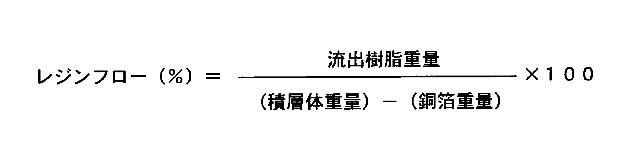
- Resin varnish for forming an adhesive layer of a multilayer flexible printed wiring board according to the present invention is obtained by adding a solvent to the above resin composition, A semi-cured resin film having a resin flow in the range of 1% to 30% when the amount is prepared in the range of 30% to 70% by weight and measured according to MIL-P-13949G in the MIL standard is formed. It is characterized by what is possible.
- the solvent mentioned here one single solvent selected from the group of methyl ethyl ketone, dimethylacetamide, dimethylformamide, etc., which is a solvent having a boiling point in the range of 50 ° C. to 200 ° C., or a mixed solvent of two or more types is used. It is preferable. This is to obtain a good semi-cured resin film as described above.
- the range of the resin solid content shown here is a range in which the film thickness can be controlled to the most accurate one when applied to the surface of the copper foil.
- the resin solid content is less than 30% by weight, the viscosity is too low and it flows immediately after application to the copper foil surface, making it difficult to ensure film thickness uniformity.
- the resin solid content exceeds 70% by weight, the viscosity increases and it becomes difficult to form a thin film on the surface of the copper foil.
- the resin varnish has a resin flow in a range of 1% to 30% when a semi-cured resin film formed using the resin varnish is measured according to MIL-P-13949G in the MIL standard. It is preferable. When the resin flow is less than 1%, it is not preferable because air entrapment or the like occurs in the uneven portions of the inner layer circuit on the surface of the inner layer core material. On the other hand, when the resin flow exceeds 30%, the resin flow becomes too large, and the thickness of the insulating layer formed using the resin layer of the resin-coated copper foil becomes non-uniform.
- the resin-coated copper foil for producing a multilayer flexible printed wiring board according to the present invention has a resin layer on the surface of the copper foil. And the said resin layer used the resin composition for the contact bonding layer formation of the above-mentioned multilayer flexible printed wiring board, It is characterized by the above-mentioned.
- the copper foil is not limited to its production method such as an electrolytic method or a rolling method, and any production method can be used. And there is no special limitation also about the thickness.
- the surface on which the resin layer of the copper foil is formed may or may not be roughened. If there exists a roughening process, the adhesiveness of copper foil and a resin layer will improve. And if it does not perform a roughening process, since it will become a flat surface, the formation capability of a fine pitch circuit will improve. Furthermore, the surface of the copper foil may be subjected to rust prevention treatment.
- rust prevention treatment it is possible to employ inorganic rust prevention using known zinc, zinc-based alloys, or the like, or organic rust prevention using an organic monomolecular film such as benzimidazole or triazole. Furthermore, it is preferable to provide a silane coupling agent treatment layer on the surface on which the resin layer of the copper foil is formed.
- the silane coupling agent layer has a role as an auxiliary agent to improve the wettability between the surface of the copper foil not particularly roughened and the resin layer, and to improve the adhesion when pressed to the base resin. Fulfill. For example, without roughening the copper foil, rust prevention treatment is performed, and silane coupling agent treatment is performed with epoxy functional silane coupling agent, olefin functional silane, acrylic functional silane, amino functional silane coupling agent. Alternatively, various products such as a mercapto-functional silane coupling agent can be used. By selecting and using a suitable silane coupling agent according to the application, the peel strength exceeds 0.8 kgf / cm. Become.
- silane coupling agent that can be used here will be described more specifically.
- the formation of the silane coupling agent layer is not particularly limited, such as a commonly used dipping method, showering method, spraying method, or the like.
- a method that can contact and adsorb the solution containing the copper foil and the silane coupling agent most uniformly can be arbitrarily employed.
- These silane coupling agents are used at a temperature of room temperature by dissolving 0.5 to 10 g / l in water as a solvent.
- the silane coupling agent forms a film by condensation bonding with OH groups protruding from the surface of the copper foil, and the effect is not significantly increased even if a solution having a very high concentration is used. Therefore, it should be originally determined according to the processing speed of the process.
- the adsorption rate of the silane coupling agent is slow, which is not suitable for general commercial profit, and the adsorption is not uniform. Moreover, even if the concentration exceeds 10 g / l, the adsorption rate is not particularly increased, which is uneconomical.
- the copper foil with resin described above is one kind of polyimide resin, polyamide resin, polyether sulfone resin, phenoxy resin, aramid resin, and polyvinyl acetal resin between the copper foil to be used and the semi-cured resin layer.
- the auxiliary resin layer which consists of 2 or more types of mixed resin. This auxiliary resin layer is formed before the semi-cured resin layer is formed.
- a resin varnish for forming either a polyimide resin, a polyamide resin, or a mixed resin of these two types is applied to the copper foil surface, a part of the solvent is removed by a drying process, and the temperature is further increased. In the drying step, it can be formed by removing the solvent and dehydrating condensation reaction.
- the thickness of the auxiliary resin layer is desirably 10 ⁇ m or less. If it exceeds 10 ⁇ m, the total thickness will increase when combined with the semi-cured resin layer referred to in the present invention, so it is difficult to reduce the total thickness when processed into a flexible printed wiring board.
- the heating at the time of forming the semi-cured resin layer is liable to cause a warping phenomenon called curl in the resin-coated copper foil, which is not preferable.
- a resin varnish is first prepared in the following step a.
- the resin varnish is applied to the surface of the copper foil and dried to form a resin-coated copper foil as a semi-cured resin film having a thickness of 10 ⁇ m to 50 ⁇ m.
- the thickness of the semi-cured resin film is less than 10 ⁇ m, the surface of the copper foil cannot be uniformly coated, and the adhesion to the base material varies depending on the location in the same plane of the printed wiring board. Is likely to occur.
- the thickness of the semi-cured resin film exceeds 50 ⁇ m, the resin layer becomes too thick and the flexibility of the flexible printed wiring board is lowered, and at the same time, the base material depending on the place in the same plane of the printed wiring board The adhesiveness tends to vary.
- Step a The above-mentioned A component is 3 to 20 parts by weight, B component is 3 to 30 parts by weight, C component is 5 to 50 parts by weight, D component is 10 to 40 parts by weight, E In the range of 20 parts by weight to 35 parts by weight of component and 0 parts by weight to 7 parts by weight of F component, the respective components are mixed to provide 0.5 to 3.0% by weight of phosphorus atoms derived from C component.
- a range-containing resin composition is used. Since each description regarding each component described here and a mixture ratio is as above-mentioned, description here is abbreviate
- Step b The resin composition is dissolved using an organic solvent to obtain a resin varnish.
- the organic solvent at this time is a solvent having a boiling point in the range of 50 ° C. to 200 ° C. as described above, one kind of single solvent selected from the group of methyl ethyl ketone, dimethylacetamide, dimethylformamide, etc. It is preferable to use a mixed solvent. This is because of the same reason as described above.
- a resin varnish having a resin solid content of 30 wt% to 70 wt% is used. The reason for determining the range of the resin solid content is the same as described above.
- the application method is not particularly limited. However, considering that the target thickness must be applied with high accuracy, a coating method and a coating apparatus corresponding to the film thickness to be formed may be appropriately selected and used. Moreover, what is necessary is just to employ
- Multilayer flexible printed wiring board according to the present invention is obtained by using the above-described resin composition for forming an adhesive layer of a multilayer flexible printed wiring board. . That is, using the resin composition according to the present invention as a resin varnish, a resin-coated copper foil is produced using the resin varnish. And it is set as the multilayer flexible printed wiring board using this copper foil with resin. At this time, there is no special limitation regarding a manufacturing process until it is set as a multilayer flexible printed wiring board using copper foil with resin. Any known manufacturing technique can be used.
- the multilayer flexible printed wiring board said to this invention says what is provided with the conductor layer containing the circuit shape of three or more layers. Hereinafter, examples will be described.
- Example of synthesis of phosphorus-containing epoxy resin A 10- (2,5-dihydroxyphenyl) -10H-9 was added to a four-necked glass separable flask equipped with a stirrer, thermometer, condenser, and nitrogen gas inlet.
- -Oxa-10-phosphaphenanthrene-10-oxide HCA-HQ, Sanko Co., Ltd.
- ethyl cellosolve 300 parts by weight
- 680 parts by weight of YDF-170 (Bisphenol F type epoxy resin manufactured by Toto Kasei Co., Ltd.) was charged, stirred while introducing nitrogen gas, heated to 120 ° C. and mixed.
- Synthesis example of phosphorus-containing epoxy resin B 10- (2,5-dihydroxyphenyl) -10H-9 was added to a four-necked glass separable flask equipped with a stirrer, thermometer, condenser, and nitrogen gas introducing device.
- -Oxa-10-phosphaphenanthrene-10-oxide HCA-HQ, Sanko Co., Ltd.
- ethyl cellosolve 300 parts by weight
- a polyamide-imide resin was synthesized.
- the obtained polyamidoimide resin had a logarithmic viscosity of 0.65 dl / g and a glass transition temperature of 203 ° C.
- Boiled solder heat resistance test After removing the copper foil layer of the outer layer of the solder heat resistance measurement sample cut out to the size of 50 mm ⁇ 50 mm described above by etching, it was immersed in boiled ion-exchanged water and subjected to boiling treatment for 3 hours. Do. And from the sample which boiled, the water
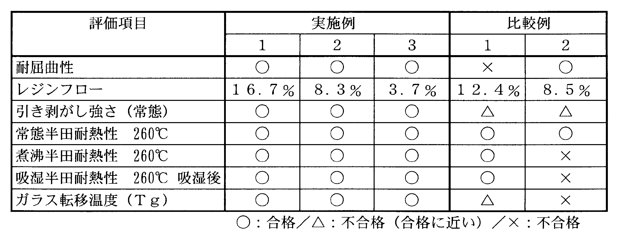
- Moisture-absorbing solder heat resistance test In the production of the above-described four-layer multilayer flexible printed wiring board, the resin-coated copper foil is held in a constant temperature and humidity chamber at a temperature of 30 ° C. and a relative humidity of 65% for 15 hours to absorb moisture. Used. The other manufacturing conditions of the four-layer multilayer flexible printed wiring board are as described above. Then, the solder heat resistance measurement sample cut out from this four-layer multilayer flexible printed wiring board and cut into a size of 50 mm ⁇ 50 mm was floated on a solder bath heated to 260 ° C., and the time until blistering was measured. . The results are shown in Table 7 so that the comparison with the comparative example is possible. The time until blistering was evaluated as ⁇ for 300 seconds or more, ⁇ for 240 to less than 300 seconds, and ⁇ for less than 240 seconds.
- This glass transition temperature (Tg) is indicated as “ ⁇ ” when it exceeds 150 ° C., “ ⁇ ” when it is 140 ° C. to 150 ° C., and “X” when it is less than 140 ° C.
- the bending resistance test by the MIT method uses a film folding fatigue tester with a tank (product number: 549) manufactured by Toyo Seiki Seisakusho as an MIT folding resistance device, with a bending radius of 0.8 mm and a load of 0.5 kgf.
- the bending resistance test film was repeatedly subjected to a bending test.
- Table 7 which shows the result, the bending resistance test film which was able to measure the number of repeated bendings of 2000 times or more was evaluated as acceptable (O), and the others were rejected.
- O acceptable
- the case where the number of times of repeated bending close to 2000 times was obtained among the failures was indicated by ⁇ , and the others were indicated by ⁇ .
- the number of repeated bendings is measured with one reciprocation of the drive head of the MIT folding apparatus as one time (one cycle).
- Example 2 instead of the resin composition of Example 1, the resin components shown in Table 1 above were used, and the resin composition having the blending ratio shown in Table 3 was used, and further dimethylacetamide was used as the solvent. The following resin varnishes were prepared. Others are the same as in the first embodiment.
- Example 2 a resin-coated copper foil was produced in the same manner as in Example 1, and the same multilayer printed wiring board evaluation as in Example 1 and the flexibility evaluation after curing of the resin layer were performed. These evaluation results are shown in Table 5 below so that the comparison with the comparative example is possible.
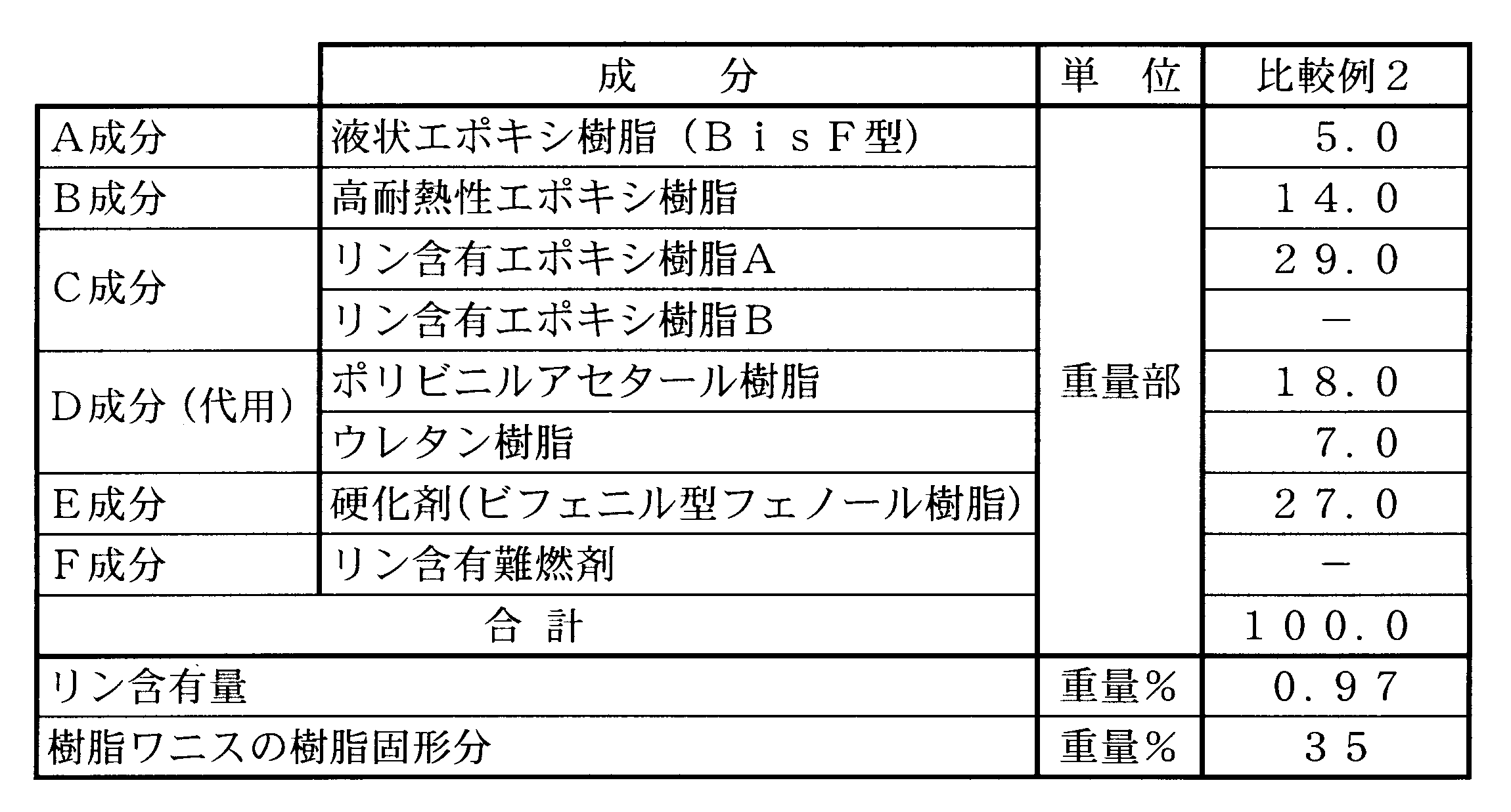
- Example 3 instead of the resin composition of Example 1, the resin components described in Table 1 above were used, and the resin composition having the blending ratio shown in Table 4 was used, and further dimethylacetamide was used as the solvent. The following resin varnishes were prepared. Others are the same as in the first embodiment.
- Example 7 a resin-coated copper foil was produced in the same manner as in Example 1, and the same multilayer printed wiring board evaluation as in Example 1 and the flexibility evaluation after curing of the resin layer were performed. These evaluation results are shown in Table 7 below so that the comparison with the comparative example is possible.
- Comparative Example 1 a resin-coated copper foil was produced by changing the curing agent of the resin composition used in the Examples to a phenol novolac resin, and the above characteristics were compared with the Examples.
- the resin-attached copper foil used here is a resin layer formed on the bonding surface of the copper foil used in Example 1, using the resin composition and resin varnish shown in Table 5 below, and provided with a resin for comparison. Copper foil was used.
- Comparative Example 2 In Comparative Example 2, the resin composition “rubber-modified polyamideimide resin such as CTBN” of the resin composition used in the examples was replaced with polyvinyl acetal resin (5000A manufactured by Denki Kagaku Kogyo Co., Ltd.) and urethane resin (Coronate manufactured by Nippon Polyurethane Industry Co., Ltd.).
- the resin-coated copper foil was manufactured by changing to (AP), and the above characteristics were compared with the examples.
- the resin-attached copper foil used here was formed by forming a resin layer on the bonding surface of the copper foil used in Example 1 using the resin composition and resin varnish shown in Table 6 below, and attaching a resin for comparison. Copper foil was used.
- the example and the comparative example are compared.
- the example shows a higher value than the comparative example and exhibits good adhesion to the inner layer core substrate.
- Example and Comparative Example there is no difference between Example and Comparative Example, and both are good.
- Example and Comparative Example 1 when looking at boiling solder heat resistance and moisture absorption solder heat resistance for estimating the quality deterioration level due to water absorption, there is not much difference between Example and Comparative Example 1, but in Example and Comparative Example 2, the direction of the Example Is clearly superior. That is, it can be understood that inclusion of “rubber-modified polyamideimide resin such as CTBN” as a component of the resin composition is important from the viewpoint of preventing moisture absorption deterioration of solder heat resistance characteristics.
- the example shows a higher value than the comparative example, and there is a high possibility of exhibiting stable performance even in a high temperature atmosphere.
- the resin composition for forming an adhesive layer of a multilayer flexible printed wiring board according to the present invention can be processed into a resin varnish and used as a resin layer constituting an insulating layer in the manufacturing process of the multilayer flexible printed wiring board.
- a resin layer using this resin composition has sufficient flexibility even after curing.
- the copper foil with resin which concerns on this invention is obtained by apply
- this resin-coated copper foil it is possible to produce a multilayer flexible printed wiring board by various methods, and the thickness of the obtained multilayer flexible printed wiring board is reduced, so that the overall weight of the substrate can be reduced. Reduction can be achieved.
Landscapes
- Chemical & Material Sciences (AREA)
- Engineering & Computer Science (AREA)
- Organic Chemistry (AREA)
- Manufacturing & Machinery (AREA)
- Microelectronics & Electronic Packaging (AREA)
- Chemical Kinetics & Catalysis (AREA)
- Medicinal Chemistry (AREA)
- Polymers & Plastics (AREA)
- Health & Medical Sciences (AREA)
- Laminated Bodies (AREA)
- Production Of Multi-Layered Print Wiring Board (AREA)
- Compositions Of Macromolecular Compounds (AREA)
- Epoxy Resins (AREA)
- Manufacturing Of Printed Wiring (AREA)
- Adhesives Or Adhesive Processes (AREA)
Abstract
Description
B成分: 高耐熱性エポキシ樹脂。
C成分: リンを含有した難燃性エポキシ樹脂。
D成分: 沸点が50℃~200℃の範囲にある溶剤に可溶な性質を備える液状ゴム成分で変成したゴム変成ポリアミドイミド樹脂。
E成分: ビフェニル型フェノール樹脂、フェノールアラルキル型フェノール樹脂の1種又は2種以上からなる樹脂硬化剤。
工程b: 前記樹脂組成物を、有機溶剤を用いて溶解し、樹脂固形分量が30重量%~70重量%の樹脂ワニスとする。
本件発明に係る多層フレキシブルプリント配線板の接着層形成用の樹脂組成物は、内層コア材となる内層フレキシブルプリント配線板の表面に外層用プリント配線板を張り合わせるための接着層を形成するために用いる樹脂組成物である。例えば、内層フレキシブルプリント配線板として、ポリイミド樹脂フィルムを基材として用い、この両面に回路を設け、且つ、必要に応じて両面の回路間の導通をビアホール等の手段で確保したものを用いる。そして、この内層フレキシブルプリント配線板の両面若しくは片面側に、絶縁層を介して新たな外層導体層を設ける。その後、外層に位置する外層導体層をエッチング加工して外層回路を形成する。この場合において、外層導体層の形成には、内層フレキシブルプリント配線板の両面若しくは片面に、接着剤層を設け、その上にプリプレグを載置して、その上に銅箔等の金属箔を配して、熱間プレス加工することで、所謂4層銅張積層板の状態とし、外層導体層をエッチング加工して多層フレキシブルプリント配線板となる。また、内層フレキシブルプリント配線板の両面若しくは片面に、樹脂付銅箔を配して、熱間プレス加工することで、所謂4層銅張積層板の状態とし、外層導体層をエッチング加工して多層フレキシブルプリント配線板となる。前者を「多層リジッドフレキシブルプリント配線板」、後者を「多層フレキシブルプリント配線板」と区分して表現する場合もあるが、一般的には両者が混在している場合があり、本件発明で言う多層フレキシブルプリント配線板は、後者の概念のものであることを明記しておく。また、ここで例示した、4層以上のプリント配線板も含む概念であることを、念のために記載しておく。


本件発明に係る多層フレキシブルプリント配線板の接着層形成用の樹脂ワニス: 本件発明に係る多層フレキシブルプリント配線板の接着層形成用の樹脂ワニスは、上述の樹脂組成物に溶剤を加えて、樹脂固形分量が30重量%~70重量%の範囲に調製し、MIL規格におけるMIL-P-13949Gに準拠して測定したときのレジンフローが1%~30%の範囲にある半硬化樹脂膜の形成が可能なことを特徴とするものである。ここで言う溶剤には、上述の沸点が50℃~200℃の範囲にある溶剤であるメチルエチルケトン、ジメチルアセトアミド、ジメチルホルムアミド等の群から選ばれる1種の単独溶剤又は2種以上の混合溶剤を用いることが好ましい。上述のように良好な半硬化樹脂膜を得るためである。そして、ここに示した樹脂固形分量の範囲が、銅箔の表面に塗布したときに、最も膜厚を精度の良いものに制御できる範囲である。樹脂固形分が30重量%未満の場合には、粘度が低すぎて、銅箔表面への塗布直後に流れて膜厚均一性を確保しにくい。これに対して、樹脂固形分が70重量%を超えると、粘度が高くなり、銅箔表面への薄膜形成が困難となる。
本件発明に係る多層フレキシブルプリント配線板製造用の樹脂付銅箔は、銅箔の表面に樹脂層を備えたものである。そして、当該樹脂層は、上述の多層フレキシブルプリント配線板の接着層形成用の樹脂組成物を用いたことを特徴とする。
本件発明に係る樹脂付銅箔の製造方法は、最初に以下の工程aで樹脂ワニスを調製する。そして、この樹脂ワニスを銅箔の表面に塗布し、乾燥させることで10μm~50μmの厚さの半硬化樹脂膜として樹脂付銅箔とすることを特徴とする。ここで、半硬化樹脂膜の厚さが10μm未満の場合には、銅箔の表面を均一に被覆することが出来ず、プリント配線板の同一面内における場所による基材との密着性にバラツキが生じやすくなる。一方、半硬化樹脂膜の厚さが50μmを超える場合には、樹脂層が厚くなりすぎて、フレキシブルプリント配線板の可撓性が低下すると同時に、プリント配線板の同一面内における場所による基材との密着性にバラツキが生じやすくなる。
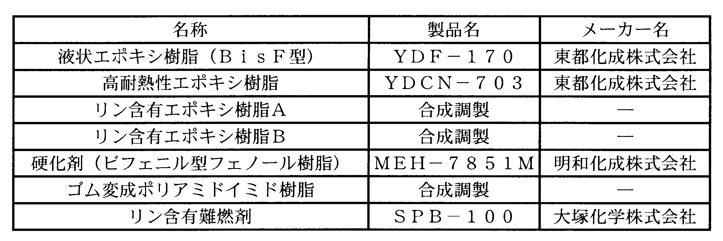
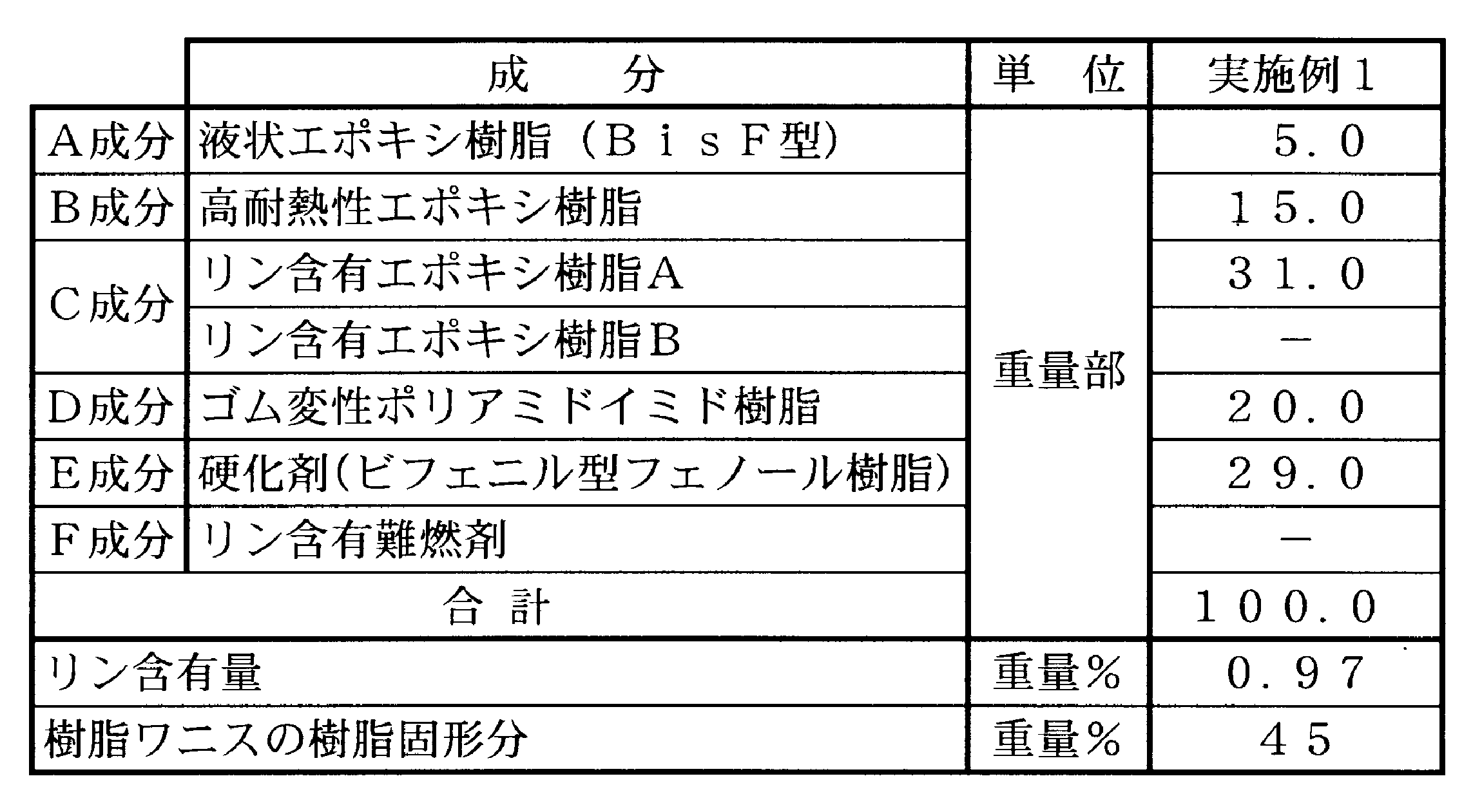
引き剥がし強さ及び常態半田耐熱性試験: 市販の0.4mm厚さのFR-4(ガラス-エポキシ基材)の両面に、18μm厚さの電解銅箔を張り合わせた銅張積層板の両面に、内層回路の形成を行い、黒化処理を行うことで内層コア材を作成した。この内層コア材の両面に、前記樹脂付銅箔を、加熱温度190℃、プレス時間90分、プレス圧40kgf/cm2の真空プレス条件で積層成形し、4層の多層フレキシブルプリント配線板を得た。この多層フレキシブルプリント配線板を用いて、10mm幅の引き剥がし試験用の直線回路を形成し、これを基板面に対して90°方向で引き剥がして「引き剥がし強さ」を測定した。また、260℃の半田浴を用いて、50mm×50mmのサイズに切り出した半田耐熱測定用試料を、この半田浴に浮かべ、ふくれが発生するまでの時間として「常態半田耐熱性」を測定した。引き剥がし強さは、1.0kgf/cmを超える場合が○、0.8kgf/cm~1.0kgf/cmの範囲が△、0.8kgf/cm未満が×として表示することとした。また、常態半田耐熱性は、300秒以上の場合が○、240秒~300秒の場合が△、240秒未満の場合が×として表示することとした。これらの評価結果は、以下の表7に、比較例との対比が可能なように示す。
上述のようにして作製した樹脂付銅箔を、圧力40Kgf/cm2、温度190℃にて90分間プレスし、さらに銅箔をエッチングによって除去することにより、厚さ46μmの単一樹脂層を作成した。そして、この単一樹脂層を30mm×5mmに切り出し、ガラス転移温度(Tg)を測定した。ガラス転移温度(Tg)の測定は、動的粘弾性測定装置(DMA)として、セイコー電子工業株式会社製の動的粘弾性測定装置(品番:SDM5600)を用い測定した。このガラス転移温度(Tg)は、150℃を超える場合に○、140℃~150℃の場合が△、140℃未満の場合が×として表示することとした。これらの評価結果は、以下の表7に、比較例との対比が可能なように示す。
ここでは、樹脂付銅箔をフッ素系の耐熱フィルムで挟み込み、加熱温度190℃、プレス圧40kgf/cm2にて真空プレスを用って、樹脂層を硬化させた。次に、硬化処理の終了した樹脂付銅箔の銅箔層のみをエッチングにより除去して、硬化した厚さ46μmの樹脂層を、15mm×150mmに切り出して耐屈曲性試験フィルムとした。そして、この耐屈曲性試験フィルムを用いて、MIT法による耐屈曲性試験を行った。MIT法による耐屈曲性試験は、MIT耐折装置として東洋精機製作所製の槽付フィルム耐折疲労試験機(品番:549)を用い、屈曲半径0.8mm、荷重0.5kgfとし、上記作成の耐屈曲性試験フィルムの繰り返し、曲げ試験を実施した。その結果を示す表7では、2000回以上の繰り返し曲げ回数の測定が出来た耐屈曲性試験フィルムを合格(○)とし、その他を不合格とした。但し、不合格の中でも2000回に近い繰り返し曲げ回数が得られた場合を△と表示して、その他を×と表示している。なお、繰り返し曲げ回数は、MIT耐折装置の駆動ヘッドの一往復を1回(1サイクル)として測定している。これらの評価結果は、以下の表7に、比較例との対比が可能なように示す。
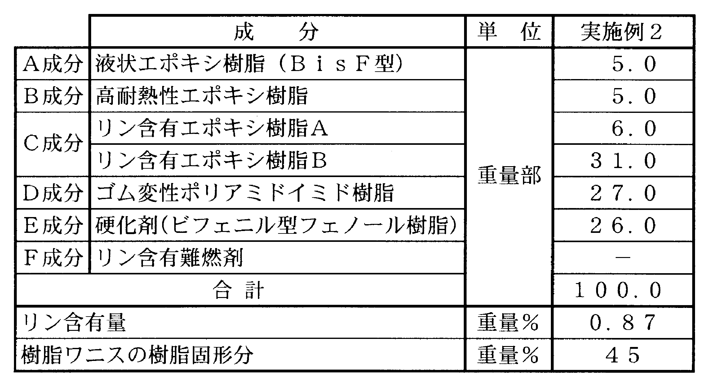
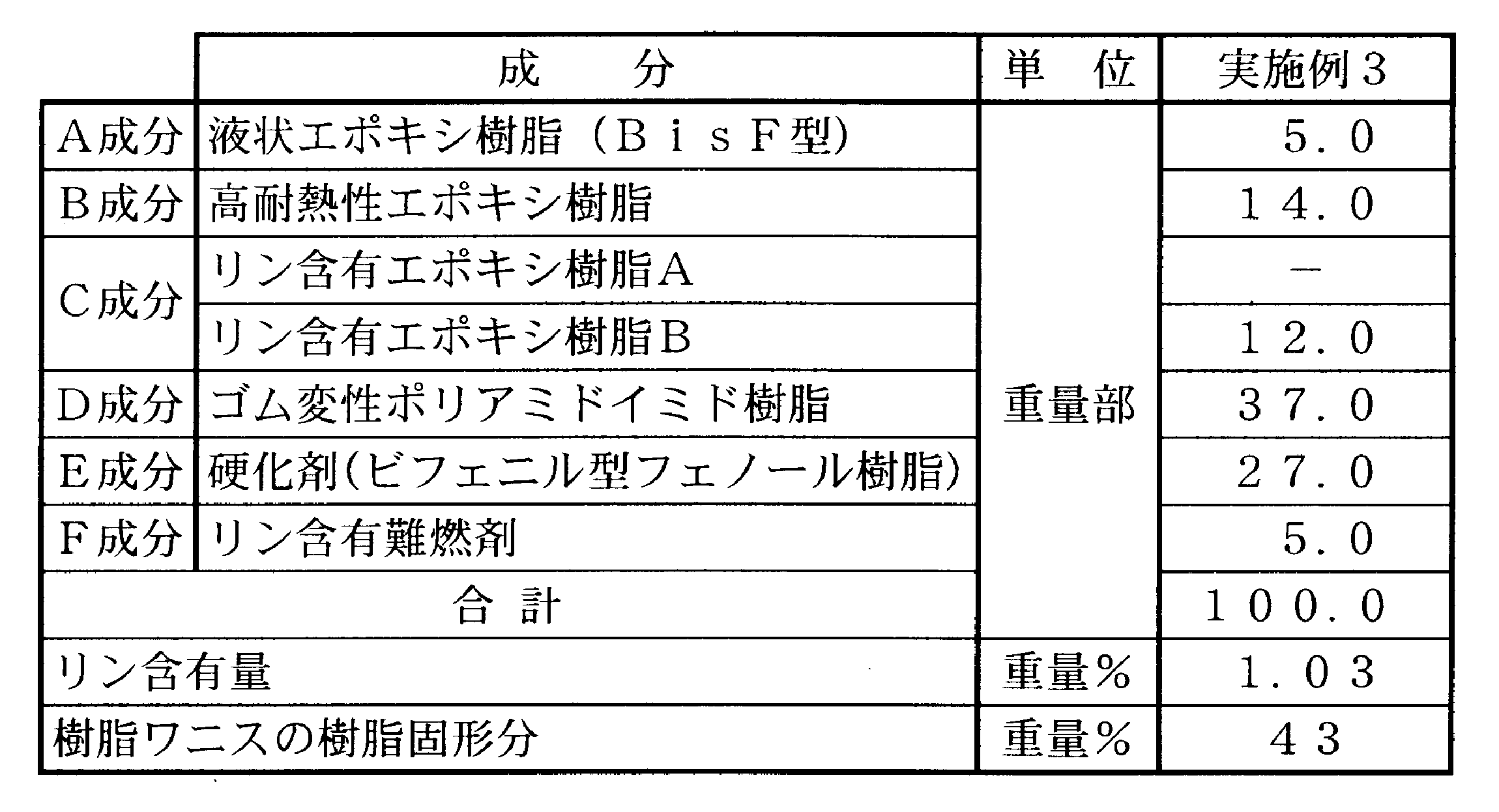
この比較例1では、実施例で用いた樹脂組成物の硬化剤をフェノールノボラック樹脂に変更して樹脂付銅箔を製造し、上記特性を実施例と比較した。ここで用いる樹脂付銅箔は、実施例1で用いた銅箔の張り合わせ面に、以下の表5に示した樹脂組成物及び樹脂ワニスを用いて、樹脂層を形成し、比較用の樹脂付銅箔とした。
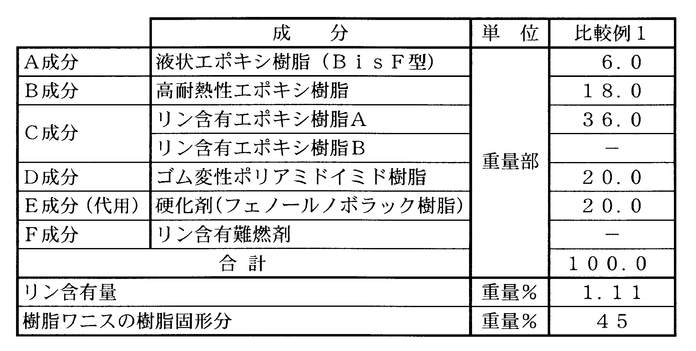
この比較例2では、実施例で用いた樹脂組成物の「CTBN等のゴム変成ポリアミドイミド樹脂」を、ポリビニルアセタール樹脂(電気化学工業株式会社製 5000A)及びウレタン樹脂(日本ポリウレタン工業株式会社製 コロネートAP)に変更して樹脂付銅箔を製造し、上記特性を実施例と比較した。ここで用いる樹脂付銅箔は、実施例1で用いた銅箔の張り合わせ面に、以下の表6に示した樹脂組成物及び樹脂ワニスを用いて、樹脂層を形成し、比較用の樹脂付銅箔とした。
Claims (10)
- 内層フレキシブルプリント配線板の表面に外層用プリント配線板を張り合わせるための接着層を形成するために用いる樹脂組成物において、
以下のA成分~E成分の各成分を含むことを特徴とした多層フレキシブルプリント配線板の接着層形成用の樹脂組成物。
A成分: エポキシ当量が200以下で、室温で液状のビスフェノールA型エポキシ樹脂、ビスフェノールF型エポキシ樹脂、ビスフェノールAD型エポキシ樹脂の群から選ばれる1種又は2種以上からなるエポキシ樹脂。
B成分: 高耐熱性エポキシ樹脂。
C成分: リンを含有した難燃性エポキシ樹脂。
D成分: 沸点が50℃~200℃の範囲にある溶剤に可溶な性質を備える液状ゴム成分で変成したゴム変成ポリアミドイミド樹脂。
E成分: ビフェニル型フェノール樹脂、フェノールアラルキル型フェノール樹脂の1種又は2種以上からなる樹脂硬化剤。 - 前記A成分~E成分の各成分に加えて、更にF成分としてエポキシ樹脂との反応性を有さないリン含有難燃剤を含む請求項1に記載の多層フレキシブルプリント配線板の接着層形成用の樹脂組成物。
- 樹脂組成物重量を100重量部としたとき、
A成分が3重量部~20重量部、B成分が3重量部~30重量部、C成分が5重量部~50重量部、D成分が10重量部~40重量部、E成分が20重量部~35重量部、F成分が0重量部~7重量部であり、
樹脂組成物重量を100重量%としたとき、C成分由来のリン原子を0.5重量%~3.0重量%の範囲含有するものである請求項1~請求項2のいずれかに記載の多層フレキシブルプリント配線板製造用の樹脂組成物。 - 前記D成分は、沸点が50℃~200℃の範囲にあるメチルエチルケトン、ジメチルアセトアミド、ジメチルホルムアミドの群から選ばれる1種の単独溶剤又は2種以上の混合溶剤に可溶な性質を備える液状ゴム成分で変成したゴム変成ポリアミドイミド樹脂である請求項1~請求項3のいずれかに記載の多層フレキシブルプリント配線板の接着層形成用の樹脂組成物。
- 前記D成分であるゴム変成ポリアミドイミド樹脂は、ポリアミドイミドとゴム性樹脂とを反応させることで得られるものである請求項1~請求項4のいずれかに記載の多層フレキシブルプリント配線板の接着層形成用の樹脂組成物。
- 請求項1~請求項5のいずれかに記載の樹脂組成物に溶剤を加えて、樹脂固形分量が30重量%~70重量%の範囲に調製し、
MIL規格におけるMIL-P-13949Gに準拠して測定したときのレジンフローが1%~30%の範囲にある半硬化樹脂膜の形成が可能なことを特徴とする樹脂ワニス。 - 銅箔の表面に樹脂層を備えた樹脂付銅箔において、
当該樹脂層は、請求項1~請求項5のいずれかに記載の多層フレキシブルプリント配線板の接着層形成用の樹脂組成物を用いて形成したことを特徴とした多層フレキシブルプリント配線板製造用の樹脂付銅箔。 - 前記銅箔の樹脂層を形成する表面は、シランカップリング剤処理層を備えるものである請求項7に記載の多層フレキシブルプリント配線板製造用の樹脂付銅箔。
- 請求項7又は請求項8に記載の多層フレキシブルプリント配線板製造用の樹脂付銅箔の製造方法であって、
以下の工程a、工程bの手順で樹脂層の形成に用いる樹脂ワニスを調製し、当該樹脂ワニスを銅箔の表面に塗布し、乾燥させることで10μm~50μmの厚さの半硬化樹脂膜として樹脂付銅箔とすることを特徴とする多層フレキシブルプリント配線板製造用の樹脂付銅箔の製造方法。
工程a: A成分が3重量部~20重量部、B成分が3重量部~30重量部、C成分が5重量部~50重量部、D成分が10重量部~40重量部、E成分が20重量部~35重量部、F成分が0重量部~7重量部の範囲において、各成分を混合して、C成分由来のリン原子を0.5重量%~3.0重量%の範囲含有する樹脂組成物とする。
工程b: 前記樹脂組成物を、有機溶剤を用いて溶解し、樹脂固形分量が30重量%~70重量%の樹脂ワニスとする。 - 請求項1~請求項5のいずれかに記載の多層フレキシブルプリント配線板の接着層形成用の樹脂組成物を用いて得られることを特徴とする多層フレキシブルプリント配線板。
Priority Applications (4)
| Application Number | Priority Date | Filing Date | Title |
|---|---|---|---|
| KR1020107026312A KR101271008B1 (ko) | 2008-05-26 | 2009-05-26 | 다층 플렉서블 프린트 배선판의 접착층 형성용 수지 조성물 |
| EP09754687.3A EP2282622A4 (en) | 2008-05-26 | 2009-05-26 | RESIN COMPOSITION FOR FORMING THE HAFT LAYERS OF A MULTILAYER FLEXIBLE PCB |
| CN2009801189431A CN102047774B (zh) | 2008-05-26 | 2009-05-26 | 多层柔性印刷电路板的粘合层形成用的树脂组合物 |
| JP2010514487A JP5430563B2 (ja) | 2008-05-26 | 2009-05-26 | 多層フレキシブルプリント配線板の接着層形成用の樹脂組成物 |
Applications Claiming Priority (2)
| Application Number | Priority Date | Filing Date | Title |
|---|---|---|---|
| JP2008136844 | 2008-05-26 | ||
| JP2008-136844 | 2008-05-26 |
Publications (1)
| Publication Number | Publication Date |
|---|---|
| WO2009145179A1 true WO2009145179A1 (ja) | 2009-12-03 |
Family
ID=41377052
Family Applications (1)
| Application Number | Title | Priority Date | Filing Date |
|---|---|---|---|
| PCT/JP2009/059591 Ceased WO2009145179A1 (ja) | 2008-05-26 | 2009-05-26 | 多層フレキシブルプリント配線板の接着層形成用の樹脂組成物 |
Country Status (7)
| Country | Link |
|---|---|
| EP (1) | EP2282622A4 (ja) |
| JP (1) | JP5430563B2 (ja) |
| KR (1) | KR101271008B1 (ja) |
| CN (1) | CN102047774B (ja) |
| MY (1) | MY155358A (ja) |
| TW (1) | TWI432510B (ja) |
| WO (1) | WO2009145179A1 (ja) |
Cited By (8)
| Publication number | Priority date | Publication date | Assignee | Title |
|---|---|---|---|---|
| JP2014019787A (ja) * | 2012-07-18 | 2014-02-03 | Sumitomo Electric Ind Ltd | 接着剤組成物並びにそれを用いた補強板付きフレキシブルプリント配線板 |
| WO2015012327A1 (ja) | 2013-07-23 | 2015-01-29 | Jx日鉱日石金属株式会社 | 表面処理銅箔、キャリア付銅箔、基材、樹脂基材、プリント配線板、銅張積層板及びプリント配線板の製造方法 |
| WO2015012376A1 (ja) | 2013-07-24 | 2015-01-29 | Jx日鉱日石金属株式会社 | 表面処理銅箔、キャリア付銅箔、基材、樹脂基材、プリント配線板、銅張積層板及びプリント配線板の製造方法 |
| JP2015534919A (ja) * | 2012-11-15 | 2015-12-07 | エランタス ピー・ディー・ジー インコーポレイテッドElantas Pdg, Inc. | 複合絶縁フィルム |
| EP3046400A2 (en) | 2015-01-16 | 2016-07-20 | JX Nippon Mining & Metals Corporation | Copper foil provided with carrier, laminate, printed wiring board, electronic device, and method for fabricating printed wiring board |
| EP3048864A2 (en) | 2015-01-21 | 2016-07-27 | JX Nippon Mining & Metals Corporation | Copper foil provided with carrier, laminate, printed wiring board, and method for fabricating printed wiring board |
| EP3054751A2 (en) | 2015-02-06 | 2016-08-10 | JX Nippon Mining & Metals Corporation | Copper foil provided with carrier, laminate, printed wiring board, electronic device and method for fabricating printed wiring board |
| EP3232747A1 (en) | 2016-04-15 | 2017-10-18 | JX Nippon Mining & Metals Corp. | Copper foil, copper foil for high-frequency circuit, carrier-attached copper foil, carrier-attached copper foil for high-frequency circuit, laminate, method of manufacturing printed wiring board, and method of manufacturing electronic device |
Families Citing this family (10)
| Publication number | Priority date | Publication date | Assignee | Title |
|---|---|---|---|---|
| CN102625580A (zh) * | 2011-01-31 | 2012-08-01 | 李洲科技股份有限公司 | 一种电路板制造流程 |
| US10406791B2 (en) | 2011-05-12 | 2019-09-10 | Elantas Pdg, Inc. | Composite insulating film |
| US10253211B2 (en) | 2011-05-12 | 2019-04-09 | Elantas Pdg, Inc. | Composite insulating film |
| CN102516894B (zh) * | 2011-11-10 | 2015-07-29 | 郑州中原应用技术研究开发有限公司 | 一种汽车内后视镜镜座专用结构胶片及其制备方法 |
| CN110863221A (zh) * | 2012-11-20 | 2020-03-06 | Jx日矿日石金属株式会社 | 附载体铜箔 |
| CN103342799B (zh) * | 2013-07-18 | 2016-03-16 | 安徽建筑大学 | 含氟、含磷及含硅的环氧树脂及其制备方法 |
| KR102041665B1 (ko) * | 2017-01-05 | 2019-11-06 | 주식회사 두산 | 동박 적층판용 접착제 |
| CN108893090B (zh) * | 2018-05-03 | 2021-03-02 | 广东生益科技股份有限公司 | 树脂组合物及其制作的胶膜、覆盖膜 |
| CN114685989A (zh) * | 2020-12-30 | 2022-07-01 | 广东生益科技股份有限公司 | 一种树脂组合物及包含其的胶膜、覆盖膜 |
| CN113861864B (zh) * | 2021-12-06 | 2022-04-12 | 中国电子科技集团公司第四十六研究所 | 一种低损耗高均匀性的粘结片及多层微波板的制备方法 |
Citations (13)
| Publication number | Priority date | Publication date | Assignee | Title |
|---|---|---|---|---|
| JPH0537153A (ja) | 1991-07-16 | 1993-02-12 | Fujitsu Ltd | 多層フレキシブルプリント基板 |
| JP2001011421A (ja) * | 1999-06-29 | 2001-01-16 | Toyobo Co Ltd | 半導体用接着剤フィルム、これを用いたリードフレーム及び半導体装置 |
| JP2002161205A (ja) * | 2000-11-24 | 2002-06-04 | Hitachi Chem Co Ltd | 難燃性耐熱性樹脂組成物、これを用いた接着剤フィルム及び接着剤付きポリイミドフィルム |
| JP2002226818A (ja) * | 2001-02-06 | 2002-08-14 | Hitachi Chem Co Ltd | 熱硬化性接着フィルム |
| JP3320670B2 (ja) | 1999-03-10 | 2002-09-03 | 松下電工株式会社 | エポキシ樹脂組成物、その製造方法、および樹脂付き金属箔、ならびにそれを用いた多層プリント配線板 |
| JP2003027028A (ja) * | 2001-07-13 | 2003-01-29 | Shin Etsu Chem Co Ltd | 接着剤組成物及びこれを用いたフレキシブル印刷配線用基板、カバーレイフィルム |
| JP2004152675A (ja) | 2002-10-31 | 2004-05-27 | Toyobo Co Ltd | 二次電池セパレーター用ポリアミドイミド樹脂、その樹脂を用いたセパレーター、およびそのセパレーターを用いた二次電池 |
| JP2005105182A (ja) * | 2003-09-30 | 2005-04-21 | Sumitomo Bakelite Co Ltd | 樹脂組成物、プリプレグおよび積層板 |
| JP2005336287A (ja) | 2004-05-26 | 2005-12-08 | Matsushita Electric Works Ltd | フレキシブルプリント配線板用熱硬化性接着シート、その製造方法及びそれを用いた多層フレキシブルプリント配線板並びにフレックスリジッドプリント配線板 |
| JP2006070176A (ja) * | 2004-09-02 | 2006-03-16 | Kyocera Chemical Corp | 難燃性接着剤組成物及びフレキシブル配線板 |
| JP2006093647A (ja) | 2004-08-26 | 2006-04-06 | Matsushita Electric Works Ltd | 多層リジッドフレキシブル配線板、多層フレキシブル配線板及びそれらの製造方法 |
| JP2006169481A (ja) * | 2004-12-20 | 2006-06-29 | Sumitomo Bakelite Co Ltd | 樹脂組成物、プリプレグおよび積層板 |
| JP2006265304A (ja) * | 2005-03-22 | 2006-10-05 | Tokai Rubber Ind Ltd | 接着剤組成物およびそれを用いたフレキシブル印刷配線板 |
Family Cites Families (4)
| Publication number | Priority date | Publication date | Assignee | Title |
|---|---|---|---|---|
| JP2005002294A (ja) * | 2003-06-16 | 2005-01-06 | Shin Etsu Chem Co Ltd | 接着剤組成物、それを用いたカバーレイフィルムおよびフレキシブル印刷配線板 |
| US20090323300A1 (en) * | 2006-04-25 | 2009-12-31 | Daisuke Fujimoto | Conductor Foil with Adhesive Layer, Conductor-Clad Laminate, Printed Wiring Board and Multilayer Wiring Board |
| KR100781582B1 (ko) * | 2006-10-11 | 2007-12-05 | 삼성전기주식회사 | 인쇄회로기판용 난연성 수지 조성물 및 이를 이용한인쇄회로기판 |
| TWI451816B (zh) * | 2007-03-20 | 2014-09-01 | Mitsui Mining & Smelting Co | And a resin composition for insulating layer constituting a printed circuit board |
-
2009
- 2009-05-26 JP JP2010514487A patent/JP5430563B2/ja not_active Expired - Fee Related
- 2009-05-26 MY MYPI2010004962A patent/MY155358A/en unknown
- 2009-05-26 KR KR1020107026312A patent/KR101271008B1/ko not_active Expired - Fee Related
- 2009-05-26 CN CN2009801189431A patent/CN102047774B/zh not_active Expired - Fee Related
- 2009-05-26 WO PCT/JP2009/059591 patent/WO2009145179A1/ja not_active Ceased
- 2009-05-26 TW TW098117408A patent/TWI432510B/zh not_active IP Right Cessation
- 2009-05-26 EP EP09754687.3A patent/EP2282622A4/en not_active Withdrawn
Patent Citations (13)
| Publication number | Priority date | Publication date | Assignee | Title |
|---|---|---|---|---|
| JPH0537153A (ja) | 1991-07-16 | 1993-02-12 | Fujitsu Ltd | 多層フレキシブルプリント基板 |
| JP3320670B2 (ja) | 1999-03-10 | 2002-09-03 | 松下電工株式会社 | エポキシ樹脂組成物、その製造方法、および樹脂付き金属箔、ならびにそれを用いた多層プリント配線板 |
| JP2001011421A (ja) * | 1999-06-29 | 2001-01-16 | Toyobo Co Ltd | 半導体用接着剤フィルム、これを用いたリードフレーム及び半導体装置 |
| JP2002161205A (ja) * | 2000-11-24 | 2002-06-04 | Hitachi Chem Co Ltd | 難燃性耐熱性樹脂組成物、これを用いた接着剤フィルム及び接着剤付きポリイミドフィルム |
| JP2002226818A (ja) * | 2001-02-06 | 2002-08-14 | Hitachi Chem Co Ltd | 熱硬化性接着フィルム |
| JP2003027028A (ja) * | 2001-07-13 | 2003-01-29 | Shin Etsu Chem Co Ltd | 接着剤組成物及びこれを用いたフレキシブル印刷配線用基板、カバーレイフィルム |
| JP2004152675A (ja) | 2002-10-31 | 2004-05-27 | Toyobo Co Ltd | 二次電池セパレーター用ポリアミドイミド樹脂、その樹脂を用いたセパレーター、およびそのセパレーターを用いた二次電池 |
| JP2005105182A (ja) * | 2003-09-30 | 2005-04-21 | Sumitomo Bakelite Co Ltd | 樹脂組成物、プリプレグおよび積層板 |
| JP2005336287A (ja) | 2004-05-26 | 2005-12-08 | Matsushita Electric Works Ltd | フレキシブルプリント配線板用熱硬化性接着シート、その製造方法及びそれを用いた多層フレキシブルプリント配線板並びにフレックスリジッドプリント配線板 |
| JP2006093647A (ja) | 2004-08-26 | 2006-04-06 | Matsushita Electric Works Ltd | 多層リジッドフレキシブル配線板、多層フレキシブル配線板及びそれらの製造方法 |
| JP2006070176A (ja) * | 2004-09-02 | 2006-03-16 | Kyocera Chemical Corp | 難燃性接着剤組成物及びフレキシブル配線板 |
| JP2006169481A (ja) * | 2004-12-20 | 2006-06-29 | Sumitomo Bakelite Co Ltd | 樹脂組成物、プリプレグおよび積層板 |
| JP2006265304A (ja) * | 2005-03-22 | 2006-10-05 | Tokai Rubber Ind Ltd | 接着剤組成物およびそれを用いたフレキシブル印刷配線板 |
Non-Patent Citations (1)
| Title |
|---|
| See also references of EP2282622A4 * |
Cited By (9)
| Publication number | Priority date | Publication date | Assignee | Title |
|---|---|---|---|---|
| JP2014019787A (ja) * | 2012-07-18 | 2014-02-03 | Sumitomo Electric Ind Ltd | 接着剤組成物並びにそれを用いた補強板付きフレキシブルプリント配線板 |
| JP2015534919A (ja) * | 2012-11-15 | 2015-12-07 | エランタス ピー・ディー・ジー インコーポレイテッドElantas Pdg, Inc. | 複合絶縁フィルム |
| WO2015012327A1 (ja) | 2013-07-23 | 2015-01-29 | Jx日鉱日石金属株式会社 | 表面処理銅箔、キャリア付銅箔、基材、樹脂基材、プリント配線板、銅張積層板及びプリント配線板の製造方法 |
| WO2015012376A1 (ja) | 2013-07-24 | 2015-01-29 | Jx日鉱日石金属株式会社 | 表面処理銅箔、キャリア付銅箔、基材、樹脂基材、プリント配線板、銅張積層板及びプリント配線板の製造方法 |
| EP3046400A2 (en) | 2015-01-16 | 2016-07-20 | JX Nippon Mining & Metals Corporation | Copper foil provided with carrier, laminate, printed wiring board, electronic device, and method for fabricating printed wiring board |
| EP3048864A2 (en) | 2015-01-21 | 2016-07-27 | JX Nippon Mining & Metals Corporation | Copper foil provided with carrier, laminate, printed wiring board, and method for fabricating printed wiring board |
| EP3054751A2 (en) | 2015-02-06 | 2016-08-10 | JX Nippon Mining & Metals Corporation | Copper foil provided with carrier, laminate, printed wiring board, electronic device and method for fabricating printed wiring board |
| US9839124B2 (en) | 2015-02-06 | 2017-12-05 | Jx Nippon Mining & Metals Corporation | Copper foil provided with carrier, laminate, printed wiring board, electronic device and method for fabricating printed wiring board |
| EP3232747A1 (en) | 2016-04-15 | 2017-10-18 | JX Nippon Mining & Metals Corp. | Copper foil, copper foil for high-frequency circuit, carrier-attached copper foil, carrier-attached copper foil for high-frequency circuit, laminate, method of manufacturing printed wiring board, and method of manufacturing electronic device |
Also Published As
| Publication number | Publication date |
|---|---|
| JPWO2009145179A1 (ja) | 2011-10-13 |
| KR101271008B1 (ko) | 2013-06-04 |
| CN102047774A (zh) | 2011-05-04 |
| MY155358A (en) | 2015-10-15 |
| TW201012867A (en) | 2010-04-01 |
| JP5430563B2 (ja) | 2014-03-05 |
| KR20110015419A (ko) | 2011-02-15 |
| TWI432510B (zh) | 2014-04-01 |
| EP2282622A4 (en) | 2015-12-09 |
| CN102047774B (zh) | 2013-07-03 |
| EP2282622A1 (en) | 2011-02-09 |
Similar Documents
| Publication | Publication Date | Title |
|---|---|---|
| JP5430563B2 (ja) | 多層フレキシブルプリント配線板の接着層形成用の樹脂組成物 | |
| JP5750049B2 (ja) | 多層フレキシブルプリント配線板の接着層形成用の樹脂組成物、樹脂ワニス、樹脂付銅箔、多層フレキシブルプリント配線板製造用の樹脂付銅箔の製造方法及び多層フレキシブルプリント配線板 | |
| JP5291553B2 (ja) | 複合樹脂層付銅箔、複合樹脂層付銅箔の製造方法、フレキシブル両面銅張積層板及び立体成型プリント配線板の製造方法 | |
| KR100767177B1 (ko) | 접착 보조제 부착 금속박, 인쇄 배선판 및 인쇄 배선판의제조 방법 | |
| JP5650908B2 (ja) | 樹脂組成物及びその樹脂組成物を用いて得られる樹脂付銅箔 | |
| TWI466970B (zh) | 用於製造電路板之氰酸酯系黏著劑樹脂組成物及包含其之可撓性覆金屬層合物 | |
| JP5704793B2 (ja) | プリント配線板の絶縁層構成用の樹脂組成物 | |
| US20120315438A1 (en) | Primer, conductor foil with resin, laminated sheet and method of manufacturing laminated sheet | |
| WO2005009093A1 (ja) | 極薄接着剤層付銅箔及びその極薄接着剤層付銅箔の製造方法 | |
| WO2014080958A1 (ja) | キャリア付銅箔、キャリア付銅箔の製造方法、プリント配線板、プリント回路板、銅張積層板、及び、プリント配線板の製造方法 | |
| JP2009144052A (ja) | プリント回路板用樹脂組成物、支持基材付き絶縁層、積層板およびプリント回路板 | |
| JP2009007424A (ja) | 接着剤組成物、並びにそれを用いた接着シート及びカバーレイフィルム | |
| JP2007326923A (ja) | フッ素樹脂基材接着用樹脂組成物及びそのフッ素樹脂基材接着用樹脂組成物を用いて得られる金属張積層板 | |
| JP6396967B2 (ja) | キャリア付銅箔及びキャリア付き銅箔を用いた銅張積層板 | |
| WO2008105563A1 (ja) | 難燃性接着剤樹脂組成物及びそれを用いたフレキシブルプリント基板用材料 | |
| JP2009132780A (ja) | 回路板用樹脂組成物、支持基材付き絶縁層、積層板及び回路板 | |
| KR20060134192A (ko) | 양면 금속 피복 적층판의 제조 방법 및 그 제조 방법에의해 얻어진 양면 금속 피복 적층판 | |
| JP4694142B2 (ja) | フレキシブルプリント配線板用基板の製造方法 | |
| JP2005223052A (ja) | プリント配線板の製造方法 | |
| JP2005298670A (ja) | 絶縁接着フィルム、プリント配線板 | |
| JP2004291393A (ja) | 絶縁層、樹脂付き金属、樹脂付きキャリアフィルムおよび多層プリント回路板 | |
| JP2008016794A (ja) | プリント配線板の製造方法 |
Legal Events
| Date | Code | Title | Description |
|---|---|---|---|
| WWE | Wipo information: entry into national phase |
Ref document number: 200980118943.1 Country of ref document: CN |
|
| 121 | Ep: the epo has been informed by wipo that ep was designated in this application |
Ref document number: 09754687 Country of ref document: EP Kind code of ref document: A1 |
|
| WWE | Wipo information: entry into national phase |
Ref document number: 2010514487 Country of ref document: JP |
|
| ENP | Entry into the national phase |
Ref document number: 20107026312 Country of ref document: KR Kind code of ref document: A |
|
| REEP | Request for entry into the european phase |
Ref document number: 2009754687 Country of ref document: EP |
|
| WWE | Wipo information: entry into national phase |
Ref document number: 2009754687 Country of ref document: EP |
|
| NENP | Non-entry into the national phase |
Ref country code: DE |