WO2009147829A1 - Image pickup apparatus - Google Patents
Image pickup apparatus Download PDFInfo
- Publication number
- WO2009147829A1 WO2009147829A1 PCT/JP2009/002449 JP2009002449W WO2009147829A1 WO 2009147829 A1 WO2009147829 A1 WO 2009147829A1 JP 2009002449 W JP2009002449 W JP 2009002449W WO 2009147829 A1 WO2009147829 A1 WO 2009147829A1
- Authority
- WO
- WIPO (PCT)
- Prior art keywords
- image
- motion
- signal
- output signal
- image sensor
- Prior art date
- Legal status (The legal status is an assumption and is not a legal conclusion. Google has not performed a legal analysis and makes no representation as to the accuracy of the status listed.)
- Ceased
Links
Images





Classifications
-
- H—ELECTRICITY
- H04—ELECTRIC COMMUNICATION TECHNIQUE
- H04N—PICTORIAL COMMUNICATION, e.g. TELEVISION
- H04N5/00—Details of television systems
- H04N5/76—Television signal recording
- H04N5/765—Interface circuits between an apparatus for recording and another apparatus
- H04N5/77—Interface circuits between an apparatus for recording and another apparatus between a recording apparatus and a television camera
- H04N5/772—Interface circuits between an apparatus for recording and another apparatus between a recording apparatus and a television camera the recording apparatus and the television camera being placed in the same enclosure
-
- H—ELECTRICITY
- H04—ELECTRIC COMMUNICATION TECHNIQUE
- H04N—PICTORIAL COMMUNICATION, e.g. TELEVISION
- H04N23/00—Cameras or camera modules comprising electronic image sensors; Control thereof
- H04N23/60—Control of cameras or camera modules
-
- H—ELECTRICITY
- H04—ELECTRIC COMMUNICATION TECHNIQUE
- H04N—PICTORIAL COMMUNICATION, e.g. TELEVISION
- H04N23/00—Cameras or camera modules comprising electronic image sensors; Control thereof
- H04N23/60—Control of cameras or camera modules
- H04N23/667—Camera operation mode switching, e.g. between still and video, sport and normal or high- and low-resolution modes
-
- H—ELECTRICITY
- H04—ELECTRIC COMMUNICATION TECHNIQUE
- H04N—PICTORIAL COMMUNICATION, e.g. TELEVISION
- H04N25/00—Circuitry of solid-state image sensors [SSIS]; Control thereof
- H04N25/40—Extracting pixel data from image sensors by controlling scanning circuits, e.g. by modifying the number of pixels sampled or to be sampled
- H04N25/42—Extracting pixel data from image sensors by controlling scanning circuits, e.g. by modifying the number of pixels sampled or to be sampled by switching between different modes of operation using different resolutions or aspect ratios, e.g. switching between interlaced and non-interlaced mode
-
- H—ELECTRICITY
- H04—ELECTRIC COMMUNICATION TECHNIQUE
- H04N—PICTORIAL COMMUNICATION, e.g. TELEVISION
- H04N25/00—Circuitry of solid-state image sensors [SSIS]; Control thereof
- H04N25/70—SSIS architectures; Circuits associated therewith
-
- H—ELECTRICITY
- H04—ELECTRIC COMMUNICATION TECHNIQUE
- H04N—PICTORIAL COMMUNICATION, e.g. TELEVISION
- H04N5/00—Details of television systems
- H04N5/76—Television signal recording
- H04N5/765—Interface circuits between an apparatus for recording and another apparatus
- H04N5/775—Interface circuits between an apparatus for recording and another apparatus between a recording apparatus and a television receiver
-
- H—ELECTRICITY
- H04—ELECTRIC COMMUNICATION TECHNIQUE
- H04N—PICTORIAL COMMUNICATION, e.g. TELEVISION
- H04N9/00—Details of colour television systems
- H04N9/79—Processing of colour television signals in connection with recording
- H04N9/7921—Processing of colour television signals in connection with recording for more than one processing mode
Definitions
- Some video camera bodies may have a switch that switches between a motion image shooting mode and a still image shooting mode, a motion image shooting trigger, and a still image shooting trigger.
- the present invention provides an image pickup apparatus configured to prevent an unnatural output image as a result of a mixture of a still image into a motion image.
- An image pickup apparatus includes an image sensor configured to output an image signal by taking an object, a driver configured to drive the image sensor so as to take the object through interlace scanning or progressive scanning, a detector configured to detect a state of the object based on the image signal output from the image sensor, and a controller configured to control the driver to select one of interlace shooting used to take the object through the interlace scanning of the image sensor, and progressive shooting used to take the object through the progressive scanning of the image sensor, in accordance with the state of the object detected by the detector.
- An image pickup apparatus includes an image sensor configured to output an image signal by taking an object, a driver configured to drive the image sensor so as to take the object through interlace scanning or progressive scanning, and a controller configured to control the driver to drive the image sensor by the interlace scanning in taking and recording a still image during waiting to take and record a motion image or during taking and recording of the motion image, and to drive the image sensor by the progressive scanning in taking and recording the still image without taking or recording the motion image.
- the present invention can provide an image pickup apparatus configured to prevent an unnatural output image as a result of a mixture of a still image into a motion image.
- Fig. 1 is a block diagram of a video camera (first embodiment).
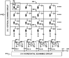
- FIG. 2 is a circuit diagram showing details of a structure of an image sensor shown in Fig. 1.
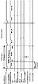
- FIG. 3 is a timing chart of the image sensor shown in Fig. 2.
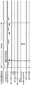
- FIG.4 is a timing chart of the image sensor shown in Fig. 2.
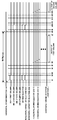
- Fig. 5 is a timing chart of the image sensor shown in Fig. 2.
- Fig. 6 is a timing chart of the image sensor shown in Fig. 2.
- Fig. 7 is a block diagram showing details of a structure of an evaluation value generator shown in Fig. 1.
- FIG. 8 is an illustrative image division of a motion vector detection (first embodiment).
- FIG.9 is an illustrative motion vector size histogram (first embodiment).
- Fig. 10 is an illustrative motion vector direction histogram (first embodiment)
- FIG.1 l is an illustrative motion vector size histogram by area (first embodiment).
- Fig. 12 is an example of a peripheral area histogram and a central area histogram.
- FIG. 13 is a block diagram of a video camera (second embodiment). Description of Embodiments
- Embodiment 1 Referring now to the accompanying drawings, a description will be given of embodiments according to the present invention.
- FIG. 1 is a block diagram of a video camera (image pickup apparatus) according to this embodiment.
- An image of an object is formed on an image sensor 2 through a lens 1, and the image sensor 2 photographs the object and outputs a video output signal S2.
- a (first) selector 5 selects one of a vertical/horizontal ("V/H") synchronization signal S3 output from a first image sensor driving circuit 3 and a V/H synchronization signal S4 output from a second image sensor driving circuit 4.
- the selector 5 supplies, as its output signal S5, the V/H synchronization signal S3 or S4 to the image sensor 2.
- the first image sensor driving circuit 3 generates the V/H synchronization signal S3 used to drive the image sensor 2 so as to convert an object image taken through interlace scanning of the image sensor 2 into an electric signal.
- the second image sensor driving circuit 4 generates the V/H synchronization signal S4 used to drive the image sensor 2 so as to convert an object image taken through progressive scanning of the image sensor 2 into an electric signal.
- the video output signal S2 corresponds to the interlace scanning when the V/H synchronization signal S3 is supplied to the image sensor 2, and to the progressive scanning when the V/H synchronization signal S4 is supplied to the image sensor 2.
- the motion image signal processing circuit 6 receives, as input signals, the video output signal S2 of the image sensor 2 and an output signal S 1 of the selector circuit 14, performs motion-image signal processing for the video output signal S2 of the image sensor 2, and outputs, as an output signal S6, a motion image signal based on the interlace scanning.
- the scan line interpolation circuit 9 receives, as an input signal, the output signal S6 of the motion image signal processing circuit 6.
- the scan line interpolation circuit 9 interpolates a scan line in the output signal S6 of the motion image signal processing circuit 6 as a video signal of the interlace scanning, converts it into a video signal of the progressive scanning, and outputs the output signal S9.
- the evaluation value generator 15 receives an input signal, the output signal S6 of the motion image signal processing circuit 6, and generates an evaluation value S 15 indicative of a state of a photographed motion image based on it.
- the image evaluation part 16 receives, as an input signal, the evaluation value S 15 of the evaluation value generator 15, and generates an image-sensor-driving determination signal S 16 indicative to the motion image driving determination and the still image driving determination based on it.
- the "motion image driving determination” is a determination that the image sensor 2 is to be driven for a motion image
- the "still image driving determination” is a determination that the image sensor 2 is to be driven for a still image. More specifically, the image evaluation part 16 determines (or evaluates) that the image sensor 2 is to be driven for a motion image, when a large motion of an object in a motion image is detected in a certain direction. In addition, the image evaluation part 16 determines that the image sensor 2 is to be driven for a still image, when no motion of an object is detected in a motion image.
- the still image signal processing circuit 10 receives as an input signal the output signal S2 of the image sensor 2, performs still-image signal processing for this signal, and outputs as an output signal SlO a video signal of the progressive scanning.
- the selector 11 receives as input signals the output signal S9 of the scan line interpolation circuit 9, the output signal SlO of the still image signal processing circuit 10, and the output signal S 14 of the selector circuit 14.
- the selector 11 selects one of the output signal S9 of the scan line interpolation circuit 9 and the output signal SlO of the still image signal processing circuit 10 based on the output signal S 14 of the selector circuit 14, and outputs the selected signal as the output signal SI l. More specifically, the selector 11 selects a third video signal of the scan line interpolation circuit 9 when the output signal S 14 of the selector circuit 14 is 0, and a second video signal of the still image signal processing circuit 10 when the output signal S 14 of the selector circuit 14 is 1.
- the still image recording processing circuit 12 receives as input signals the output signal Sl 1 of the selector 11 and the output signal S 132 of the CPU 13.
- the still image recording processing circuit 12 records the output signal Sl 1 of the selector 11 in a still image recording media 19 when a command to record a still image is issued, and performs no process when no command to record a still image is issued.
- the CPU (controller) 13 outputs a signal S 131 indicating that a motion image is being recorded or that recording of a motion image recording is being waited, and a signal S 132 indicating that a command to record a still image is issued. More specifically, the CPU 13 outputs the output signal S 131 of 0 when no motion image is being recorded or that no recording of a motion image is being waited, and the output signal S 131 of 1 when a motion image is being recorded or that recording of a motion image is being waited. The CPU 13 outputs the output signal S 132 of 0 when no command to record a still image is issued, and the output signal S 131 of 1 when a command to record a still image is issued.
- the operating part 20 includes a release button, an operation dial, a variety of buttons, a switch, and a lever, and informs the CPU 13 that a photographer has issued a command to take and record a motion or still image.
- the CPU 13 determines whether the command to take or record a motion or still image is issued, based on a notice from the operating part 20.
- the selector circuit 14 receives as input signals the output signal S 132 of the CPU 13 and the image-sensor-driving determination signal S 16, and outputs as an output signal S 14 a synchronization signal provided to the image sensor 2 and an output signal that determines an operation of the motion image signal processing circuit 6.
- the selector circuit 14 outputs an output signal S 14 of 0 (first state signal) when receiving the output signal S 16 form the image evaluation part 16 which indicates a determination signal that the image sensor 2 is to be driven for a motion image or when receiving the output signal S 132 from the CPU 13 which indicates that a command to take and record a motion image from a standby state or a command to take and record a still image is issued during the motion image shooting.
- the selector circuit 14 outputs an output signal S 14 of 1 (second state signal) when receiving the output signal S 16 form the image evaluation part 16 which indicates a determination that the image sensor 2 is to be driven for a still image or when receiving the output signal S 132 from the CPU
- the selector 5 selects the first image sensor driving circuit 3 when the selector circuit
- the selector 5 selects the second image sensor driving circuit 3 when the selector circuit 14 outputs the output signal S 14 of 1 (second stage signal). This configuration can prevent an unnatural output motion image as a result of a mixture of a still image into a motion image.
- Fig. 2 is a circuit diagram showing a structure of the image sensor 2, and shows only sixteen pixels of four vertical columns and four horizontal rows for description purposes, but actually there are more pixels of 1,080 vertical columns and horizontal 1,920 rows.
- reference numeral 201 denotes a photoelectric conversion pixel part, including a photodiode 202, a pixel readout switch 203, and a charge voltage conversion buffer 204.
- the image sensor 2 has a plurality of photoelectric conversion elements.
- Reference numerals 205-1 to 205-4 are column selection lines for the first to fourth columns, and column selection lines for the fifth to 1,080 th are omitted.
- Reference numerals 206-1 to 206-4 are row selection lines for the first to fourth rows, and row selection lines for the fifth to 1,920 th rows are omitted.
- Reference numerals 207-1 to 207-4 are row selection switches for first to fourth rows, and row selection switches for the fifth to 1,920 th rows are omitted.
- Reference numerals 208-1 to 208-4 are selection switches for first horizontal capacitors for the first to fourth rows, and selection switches for the fifth to 1,920 th rows are omitted.
- Reference numerals 209-1 to 209-4 are selection switches for second horizontal capacitors for the first to fourth rows, and selection switches for the fifth to 1,920 th rows are omitted.
- Reference numerals 210-1 to 210-4 are first horizontal capacitors for the first to fourth rows, and the first horizontal capacitors for the fifth to 1,920 th rows are omitted.
- Reference numerals 211-1 to 211-4 are second horizontal capacitors for the first to fourth rows, and the second horizontal capacitors for the fifth to 1,920 th rows are omitted.
- Reference numerals 212-1 to 212-4 are horizontal driving switches for the first to fourth rows, and horizontal driving switches for the fifth to 1,920 th rows are omitted.
- Reference numeral 213 denotes a vertical scanning circuit
- reference numeral 214 denotes a horizontal scanning circuit.
- Reference numeral 215 denotes a vertical synchronization signal input which is input from the first image sensor driving circuit 3 or the second image sensor driving circuit 4 via the selector 5.
- Reference numeral 216 denotes a horizontal synchronization signal input which is input from the first image sensor driving circuit 3 or the second image sensor driving circuit 4 via the selector 5.
- Reference numeral 217 denotes an output signal buffer, and reference numeral 218 denotes a video signal output.
- the image sensor 2 operates as follows based on a synchronization signal provided by the first image sensor driving circuit 3 or the second image sensor driving circuit 4 via the selector 5.
- FIGs. 3 to 6 are timing charts of the image sensor 2.
- vertical driving for a vertical blanking period of 2OH and a vertical effective period of 540H is provided.
- the vertical scanning circuit 213 scans the column selection lines every two columns per one horizontal synchronization period after the vertical blanking period.
- the column selection lines 205-1 and 205-2 for the first and second columns, and the column selection lines 205-3 and 205-4 for the third and fourth columns, ... the column selection lines for the 1079 th and 1080 th columns are scanned in these combinations.
- Fig. 4 shows detailed operations of the column selection lines and the horizontal scanning circuit 214.
- the horizontal synchronization signal is asserted, in the subsequent time period tl-t2, the column selection line 205-1 for the first column is asserted, and the photoelectric conversion signals from 1920 photoelectric conversion elements connected to the column selection line 205-1 for the first column are simultaneously read out to the 1920 row signal lines.
- the row selection switch 207 and the selection switch 208 for the first horizontal capacitor are also simultaneously asserted.
- reference numeral 207 represents “207-1,” “207-2,” ...
- reference numeral 208 represents “208-1,” “208-2,” ...
- reference numeral 209 represents “209-1,” “209-2,” ... .
- the photoelectric conversion signals from the 1920 photoelectric conversion elements connected to the column selection line 205-1 for the first column are accumulated in the first horizontal capacitor (such as 210-1).
- the column selection line 205-2 for the second column is asserted, and the photoelectric conversion signal from the 1,920 photoelectric conversion elements connected to the column selection line 205-2 for the second column are read out.
- the row selection switches 207 and the selection switches 209 for the second horizontal capacitors are also simultaneously asserted. Therefore, the photoelectric conversion signals from the 1,920 photoelectric conversion elements connected to the column selection line 205-2 for the second column are accumulated in the second horizontal capacitor (such as 211-1).
- both the selection switches 208 for the first horizontal capacitors and the selection switches 209 for the second horizontal capacitors are asserted.
- the photoelectric conversion signals for the first column and the photoelectric conversion signals for the second column held by the first capacitors (such as 210-1) and the second horizontal capacitors (such as 211-1) are averaged.
- the horizontal driving switches (such as 212-1) for the 1,920 rows are sequentially asserted.
- the video signal made by vertically averaging the 1,920 photoelectric conversion element outputs for the first and second columns passes the output signal buffer 217, and is output from the video signal 218.
- an operation of the next horizontal synchronization period is performed (average reading of the photoelectric conversion signals for the third and fourth columns).
- the vertical scanning circuit 213 scans the column selection lines every two columns per one horizontal synchronization period after the vertical blanking period.
- This configuration can change a combination of the averaging for two adjacent vertical lines.
- the second field has an interlace- scanning relationship with the first field.
- vertical driving for a vertical blanking period of 2OH, a vertical effective period of l,080H, and a dummy period of 2OH is provided.
- the vertical scanning circuit 213 asserts every one column of the column selection line per one horizontal synchronization period after the vertical blanking period, and sequentially scans the column selection lines up to the column selection line for the 1,080 th column. All the pixels are driven in a period of the two fields.
- Fig. 6 shows detailed operations of the column selection lines and the horizontal scanning circuit 214.
- the horizontal synchronization signal is asserted, in the subsequent time period tl-t2, the column selection line 205-1 for the first column is asserted, and the row selection switches 207 and the selection switches 208 for the first horizontal capacitors are simultaneously asserted.
- the photoelectric conversion signals from the 1,920 photoelectric conversion elements connected to the column selection line 205-1 for the first column are accumulated in the first horizontal capacitors (such as 210-1).
- the horizontal driving switches (such as 212-1) for the 1,920 rows are sequentially asserted.
- the 1,920 photoelectric conversion signals for the first column pass the output signal buffer 217, and are output from the video signal output 218.
- the next horizontal synchronization period follows (reading of the photoelectric conversion signals for the second column). As a result, the video output as a result of progressive reading of all pixels is generated.
- the image sensor 2 when the selector 5 selects the V/H synchronization signal S3 output from the first image sensor driving circuit 3, the image sensor 2 outputs as the output signal S2 the video signal of the interlace scanning at the field period.
- the output signal S5 from the selector 5 is the V/H synchronization signal S4 output from the image sensor driving circuit 4, the image sensor 2 outputs as the output signal S2 the video signal of the progressive scanning at the frame period.
- the selector 5 When the output signal S 14 from the selector circuit 14 is 0, the selector 5 outputs as the output signal S5 the V/H synchronization signal S3 output from the first image sensor driving circuit 3 so that the image sensor 2 can be driven by the interlace scanning at the field period. On the other hand, when the output signal S 14 from the selector circuit 14 is 1, the selector 5 outputs as the output signal S5 the V/H synchronization signal S4 output from the second image sensor driving circuit 4 so that the image sensor 2 can be driven by the progressive scanning at the frame period.
- the motion signal processing circuit 6 receives, as input signals, the video output signal S2 of the image sensor 2 and the output signal S 14 of the selector circuit 14.
- the motion image signal processing circuit 6 performs a variety of motion-image processes, such as an aperture correction, a gamma correction, a brightness adjustment, and a white balance, and a resize process to an angle of view of a format for the motion image recording, and outputs the resultant signal as the output signal S6.
- the output signal S 14 of the selector circuit 14 is 1
- the output signal S 6 of the motion image signal processing circuit 6 is valid only to the motion image display processing circuit 8.
- the motion image signal processing circuit 6 performs a resize process so that the output signal S2 of the image sensor 2 can have the same angle of view as that of the motion image processing time, and outputs the output signal S6 as the video signal of the interlace scanning.
- the motion image signal processing circuit 6 may output as the output signal S6 the image signal indicating that a still image is recorded.
- the motion image recording processing circuit 7 records the output signal S6 of the motion image signal processing circuit 6 in the motion image recording medium, because a motion image is being recorded.
- the motion image recording processing circuit 7 does not perform any processes, because no motion image is being recorded.
- the scan line interpolation circuit 9 performs a scan line interpolation process of the interlace scanning, and outputs as the output signal S9 the video signal of the progressive scanning.
- the scan line interpolation process utilizes a field memory to delay an input signal by one field, performs a motion determination and a gradient determination based on the information of the current field and one previous field, and generates an interpolation line signal.
- the video signal of the progressive scanning is output by outputting the interpolated line signal and the input signal.
- This scan line interpolation process is one example, and an interpolation signal may be generated using a plurality of fields.
- the still image signal processing circuit 10 performs a variety of still-image processes, such as an aperture correction, a gamma correction, a brightness adjustment, and a white balance, and outputs the resultant signal as the output signal SlO.
- the selector 11 selects one of the output signal S9 of the scan line interpolation circuit 9 and the output signal SlO of the still image signal processing circuit 10, and outputs the selected signal as the output signal SI l.
- the selector 11 When the output signal S 14 of the selector circuit 14 is 0, the selector 11 outputs as the output signal SI l the output signal S9 of the scan line interpolation circuit 9.
- the selector 11 when the output signal S 14 of the selector circuit 14 is 1, the selector 11 outputs as the output signal SI l the output signal SlO of the still image signal processing circuit 10.
- the still image recording processing circuit 12 receives, as input signals, the output signal Sl 1 of the selector 11 and the output signal S 132 of the CPU 13.
- the output signal S 132 of the CPU 13 of 1 means that a command to record a still image is issued, and thus the still image recording processing circuit 12 records the output signal Sl 1 of the selector 11 in the still image recording medium.
- the output signal S 132 of the CPU 13 of 0 means that no command to record a still image is issued, and thus the still image recording processing circuit 12 performs no processes.
- the evaluation value generator 15 generates an evaluation value S 15 indicative of a state of a photographed motion image.
- Fig. 7 is a block diagram of a structure of the evaluation value generator 15.
- reference numeral 701 denotes an input terminal that receives the output signal S6 from the motion image signal processing circuit 6.
- Reference numeral 702 denotes a frame memory.
- Reference numeral 703 denotes a motion vector detection circuit.
- Reference numeral 704 is a motion vector size histogram generation circuit.
- Reference 705 denotes a motion vector direction histogram generation circuit.
- Reference numeral 706 denotes a motion vector size histogram generation circuit by area.
- Reference numeral 707 denotes a first histogram determination circuit.
- Reference numeral 708 denotes a second histogram determination circuit.
- Reference numeral 709 denotes a third histogram determination circuit.
- Reference numeral 710 is a specific object detection circuit.
- Reference numeral 711 is a main object determination part.
- Reference numeral 712 denotes a brightness level evaluation value detection circuit.
- Reference numeral 713 denotes an object brightness determination part.
- Reference numeral 714 a color evaluation value detection circuit.
- Reference numeral 715 denotes an object color determination part.
- the video signal S6 that has undergone motion-image signal processing and been input from the input terminal 701 is input each of the frame memory 702, the motion vector detection circuit 703, the specific object detection circuit 710, the brightness level evaluation value detection circuit 712, and the color evaluation value detection circuit 714.
- the motion vector detection circuit 703 calculates a motion vector based on the video signal S701 and the video signal S702 that has been delayed by one frame by the frame memory 702.
- the motion vector is calculated for each of small 256 blocks made by dividing the shooting angle of view by sixteen in length and sixteen in width, as shown in Fig. 8, and is separated into a size and a direction.
- size data S703-1 and motion vector's direction data S703-2 are generated for each of the 256 motion vectors.
- the size data S703-1 of the motion vector is input into the motion vector size histogram generation circuit 704 and the motion vector size histogram generation circuit by area 706.
- the direction data S703-2 of the motion vector is input into the motion vector direction histogram generation circuit 705.
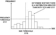
- the motion vector size histogram generation circuit 704 generates motion vector histogram data S704 based on size data S703-1 of the 256 motion vectors, as shown in Fig. 9, and inputs it in the first histogram determination circuit 707.
- the first histogram determination circuit 707 also receives a first motion size detection threshold S716 and a first motion size frequency threshold S717.
- the first histogram determination circuit 707 determines, as shown in Fig. 9, whether there are a predetermined number of blocks or more in each of which a motion having a predetermined size is detected, and outputs a first motion determination output S707. In a situation where the first motion determination output S707 is asserted, it is determined that the object of the photographed motion image is moving with a predetermined size over a predetermined area.
- the motion vector direction histogram generation circuit 705 generates motion vector direction histogram data S705 based on the direction data S703-2 of the 256 motion vectors, as shown in Fig. 10, and inputs it the second histogram determination circuit 708.
- the second histogram determination circuit 708 also receives the motion direction frequency threshold S718.
- the second histogram determination circuit 708 determines, as shown in Fig. 10, whether there are a predetermined number of blocks or more in each of which a motion in a predetermined direction is detected, and outputs the second motion determination output S708. In a situation where the second motion determination output S708 is asserted, it is determined that the object of the photographed motion image is conspicuously moving in the specific direction.
- the motion vector size histogram generation circuit by area 706 receives the size data S703-1 of the 256 motion vectors. As shown in Fig. 11, the motion vector size histogram generation circuit by area 706 divides the 256 motion vectors into a screen central part and a screen peripheral part, generates the motion vector size histogram data S706 for each area, and inputs it into the third histogram determination circuit 709.
- the third histogram determination circuit 709 also receives the second motion size detection threshold S719 and the second motion size frequency threshold S720.
- the third histogram determination circuit 709 determines, as shown in Fig. 12, whether there are a predetermined number of blocks or more in each of which a motion having a predetermined size is detected for each of the screen central part and the screen periphery part, and outputs a third motion determination output S709 when it is determined that the motion exits only in the peripheral part.
- Fig. 12A shows a peripheral area histogram
- Fig. 12B shows a central area histogram
- the specific object detection circuit 710 detects, based on the input video signal
- the main object determination part 711 determines one specific object based on the plurality of pieces of object position information S710, and outputs the main object position information S711. By referring to the main object position information S711, it can be determined whether a specific object exists in the photographed motion image.
- the brightness level evaluation value detection circuit 712 generates a brightness level evaluation value S712 based on the video signal S701, for example, by extracting a brightness signal, by dividing a screen into a plurality of blocks for the brightness signal of the photographed motion image, and by generating an integral value of a brightness signal for each of a plurality blocks.
- the brightness level evaluation value S712 and the object brightness determination level S721 are input into the object brightness determination part 713.
- the object brightness determination part 713 compares a brightness evaluation value in the screen central part with the object brightness determination level S721, and outputs the object's brightness level determination result S713. By referring to the object's brightness level determination result S713, a value of the object's brightness relative to the object brightness determination level S721 can be determined.
- the color evaluation value detection circuit 714 generates a specific color evaluation value S714 based on the video signal S701, for example, by extracting a color difference signal, by dividing a screen into a plurality of blocks for a color difference signal of the photographed motion image, and by integrating only color difference signals having specific values for each of a plurality blocks.
- the specific color evaluation value S714 and the object color determination level S722 are input into the object color determination part 715.
- the object color determination part 715 determines, for example, whether a specific color concentrates on the screen central part, and outputs an object's color level determination result S715. By referring to the object's color level determination result S715, it is determined whether the color of the object is contained in a specific color difference signal range.
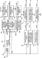
- the image evaluation part 16 provides a motion image driving determination and a still image driving determination based on the evaluation value S 15, as described later. Initially, the image evaluation part 16 generates a motion-image-driving determination signal S 16 based on the first motion determination output S707 and the second motion determination output S708, when a large motion having a predetermined size or larger in a predetermined direction in the photographed motion image is detected. This configuration can prevent unnaturalness of a large movement of the object that is likely to be visually detected.
- the image evaluation part 16 generates, based on the third motion determination output S709, a determination signal S 16 that indicates that the image sensor 2 should be driven for a still image, when it is determined that a photographer is intentionally panning (when the peripheral part has a larger motion than the central part in the motion image).
- the image evaluation part 16 generates, based on the main object position information S711, a determination signal S 16 that indicates that the image sensor 2 should be driven for a still image on the premise that a photographer is taking a desired object, when it is determined that a specific portion, such as a face of an object, exits in the photographed motion image.
- the image evaluation part 16 determines, based on the object's brightness level determination result S713, that the object's brightness is lower than the threshold, the image evaluation part 16 generates a still-image-driving determination signal S 16.
- the image evaluation part 16 determines, based on the object's color level determination result S715, that the object's color is close to yellow (or within a specific color difference range that has yellow at the center), the image generation part 16 generates a motion-image-driving determination signal S 16.
- the image evaluation part 16 can change controls over unnaturalness depending upon a level at which the large movement of the object is visually detected.
- the image evaluation part 16 cannot uniquely determine whether the determination signal S 16 determines motion image driving or still image driving based on S707, S708, S709, S711, S713, and S715 in the evaluation value S15. In these cases, the image evaluation part 16 may use a predetermined priority order, a majority rule, a known multivariate analysis result, a known neural network determination result, etc.
- the selector circuit 14 receives, as input signals, the output signal S 132 of the CPU 13 and the determination signal S 16 used to drive the image sensor.
- the output signal S 132 of the CPU 13 is 1 and the determination signal S 16 determines motion image driving
- the output signal S 14 of the selector circuit 14 becomes 0 and the image sensor 2 is controlled under field motion image driving of the interlace scanning.
- the motion image signal processing circuit 6 provides field motion image processing by the interlace scanning, and the field motion image is supplied to the motion image recording processing circuit 7 and the motion image display processing circuit 8.
- the selector 11 communicates the output signal S9 of the scan line interpolation circuit 9 to the still image recording processing circuit 12.
- the output signal S 14 of the selector circuit 14 becomes 1 and the image sensor 2 is controlled under still image driving of the progressive scanning.
- the output signal S6 of the motion image signal processing circuit 6 is valid only relative to the motion image display processing circuit 8, the output signal S2 of the image sensor 2 is resized so that it has the same angle of view as that for the motion image processing time, and is output as a video signal of the interlace scanning. Alternatively, an image indicating that the still image is recorded may be output as an output signal S6.
- the still image signal processing circuit 10 provides still image processing by the progressive scanning, and the selector 11 communicates the output signal SlO of the still image signal processing circuit 10 to the still image recording processing circuit 12.
- Fig. 13 is a block diagram of a video camera (image pickup apparatus) according to a second embodiment.
- Those elements in Fig. 13, which are the same as corresponding elements in Fig. 1, are designated by the same reference numerals, and a duplicate description will be omitted. Since the structure and timing chart of the image sensor 2 in this embodiment are similar to those of FIGs. 2-6 in the first embodiment, a description thereof will be omitted.
- An image of the object is formed onto the image sensor 2 through the lens 1, and the image sensor 2 photographs the object and outputs the video output signal S2.
- the (first) selector 5 selects one of the V/H synchronization signal S3 output from the first image sensor driving circuit 3 and the V/H synchronization signal S4 output from the second image sensor driving circuit 4.
- the V/H synchronization signal S3 or S4 selected by the selector 5 is supplied as its output signal S5 to the image sensor 2.
- the first image sensor driving circuit 3 generates the V/H synchronization signal S3 configured to drive the image sensor 2 so as to convert the object image taken through the interlace scanning of the image sensor 2 into an electric signal.
- the second image sensor driving circuit 4 generates the V/H synchronization signal S4 configured to drive the image sensor 2 so as to convert the object image taken through the progressive scanning of the image sensor 2 into an electric signal.
- the video output signal S2 corresponds to the interlace scanning when the V/H synchronization signal S3 is supplied to the image sensor 2, and corresponds to the progressive scanning when the V/H synchronization signal S4 is supplied to the image sensor 2.
- Reference numeral 30 denotes an analog front end (“AFE”) that includes a correlated double sampling (“CDS”) circuit and an analog-to-digital (AfD) conversion circuit.
- the CDS circuit is a circuit configured to remove a reset noise that is dominant in the noises contained in the video output signal S2 of the image sensor 2.
- the A/D conversion circuit is a circuit configured to convert an analogue image into a digital image.
- the AFE 30 is a circuit configured to convert an analogue signal into a digital signal that is processible by the motion image signal processing circuit 6.
- the motion signal processing circuit 6 receives, as input signals, the output signal S30 of the AFE 30 and the output signal S 14 of the selector circuit 14, performs motion-image signal processing for the output signal S30 of the AFE 30, and outputs as the output signal S6 the motion image signal based on the interlace scanning.
- the motion image recording processing circuit 7 receives, as input signals, the output signal S6 of the motion image signal processing circuit 6 and the output signal S 131 of the CPU 13, and records the output signal S6 of the motion image signal processing circuit 6 in the motion image recording media 17 when the motion image is being recorded, and provides no process when the motion image is not being recorded.
- the motion image display processing circuit 8 receives as an input signal the output signal S6 of the motion image signal processing circuit 6, and displays the output signal S6 of the motion image signal processing circuit 6 in the display 18 attached to the image pickup apparatus.
- the motion image display processing circuit 8 displays the output signal S6 of the motion image signal processing circuit 6 whether the selector 5 selects the first image sensor driving circuit 3 or the second image sensor driving circuit 4.
- the scan line interpolation circuit 9 receives as an input signal the output signal S6 of the motion image signal processing circuit 6.
- the scan line interpolation circuit 9 interpolates a scan line in the output signal S6 of the motion image signal processing circuit 6 as the video signal of the interlace scanning, converts it into the video signal of the progressive scanning, and outputs the output signal S9.
- the selector 11 receives as receiving signals the output signal S9 of the scan line interpolation circuit 9, the output signal SlO of the still image signal processing circuit 10, and the output signal S 131 of the CPU 13.
- the selector 11 selects one of the output signal S9 of the scan line interpolation circuit 9 and the output signal SlO of the still image signal processing circuit 10, based on a value of the output signal S 131 of the CPU 13, and outputs the selected signal as the output signal SI l. More specifically, the selector 11 selects the third video signal of the scan line interpolation circuit 9 when the output signal S 131 of the CPU 13 is 0, and selects the second video signal of the still image signal processing circuit 10 when the output signal S 131 of the CPU 13 is 1.
- the still image recording processing circuit 12 receives, as input signals, the output signal Sl 1 of the selector 11 and the output signal S 132 of the CPU 13.
- the still image recording processing circuit 12 records the output signal Sl 1 of the selector 11 in the still image recording media 19 when a command to record a still image is issued, and no process is performed when no command to record a still image is issued.
- the operating part 20 includes a release button, an operation dial, a variety of buttons, a switch, and a lever, and informs the CPU 13 that a photographer has instructed to take and record a motion or still image.
- the CPU 13 determines whether a command to take or record a motion or still image is issued, based on a notice from the operating part 20.
- the selector circuit 14 receives, as input signals, the output signals S 131 and S 132 of the CPU 13, and outputs a synchronization signal to be provided to the image sensor 2 and an output signal S 14 that determines an operation of the motion image signal processing circuit 6.
- the output signal S 131 from the CPU 13 of 1 indicating that a motion image is being recorded or recording of a motion image is waited is output, and the output signal S 132 of 1 indicating that a command to record a still image is output, it is understood that a command to record a still image is issued when the motion image is being recorded or recording of the motion image is waited.
- the selector circuit 14 receives as input signals the outputs S 131 and S 132 of the
Landscapes
- Engineering & Computer Science (AREA)
- Multimedia (AREA)
- Signal Processing (AREA)
- Studio Devices (AREA)
Abstract
Description
3 First image sensor driving circuit
4 Second image sensor driving circuit
13 CPU
15 Evaluation value generation part
Claims (8)
an image sensor configured to output an image signal by taking an object image;
a driver configured to drive the image sensor so as to take the object image through interlace scanning or progressive scanning;
a detector configured to detect a state of the object image based on the image signal output from the image sensor; and
a controller configured to control the driver to select one of interlace image shooting used to take the object image through the interlace scanning of the image sensor, and progressive image shooting used to take the object through the progressive scanning of the image sensor, in accordance with the state of the object image detected by the detector.
a motion image signal processor configured to output a motion image based on the image signal that is obtained through the interlace scanning of the image sensor;
a still image signal processor configured to output a still image based on the image signal that is obtained through the progressive scanning of the image sensor; and
a scan line interpolator configured to output a still image by interpolating a scan line in the image signal that is obtained by the interlace scanning of the image sensor.
an image sensor configured to output an image signal by taking an object image;
a driver configured to drive the image sensor so as to take the object image through interlace scanning or progressive scanning; and
a controller configured to control the driver to drive the image sensor by the interlace scanning in shooting and recording a still image during waiting to shoot and record a motion image or during shooting and recording of the motion image, and to drive the image sensor by the progressive scanning in shooting and recording the still image without shooting or recording the motion image.
a motion image signal processor configured to output a motion image based on the image signal that is obtained through the interlace scanning of the image sensor;
a still image signal processor configured to output a still image based on the image signal that is obtained through the progressive scanning of the image sensor; and
a scan line interpolator configured to output a still image by interpolating a scan line in the image signal that is obtained by the interlace scanning of the image sensor.
Priority Applications (4)
| Application Number | Priority Date | Filing Date | Title |
|---|---|---|---|
| EP09758096.3A EP2286582B1 (en) | 2008-06-03 | 2009-06-02 | Image pickup apparatus |
| US12/995,654 US8803996B2 (en) | 2008-06-03 | 2009-06-02 | Image pickup apparatus for preventing unnatural motion of a motion image |
| KR1020107026669A KR101241379B1 (en) | 2008-06-03 | 2009-06-02 | Image pickup apparatus |
| CN2009801208409A CN102057664B (en) | 2008-06-03 | 2009-06-02 | Image pickup apparatus |
Applications Claiming Priority (4)
| Application Number | Priority Date | Filing Date | Title |
|---|---|---|---|
| JP2008145333A JP5408907B2 (en) | 2008-06-03 | 2008-06-03 | Imaging device |
| JP2008-145333 | 2008-06-03 | ||
| JP2008168493A JP5473260B2 (en) | 2008-06-27 | 2008-06-27 | Imaging device |
| JP2008-168493 | 2008-06-27 |
Publications (1)
| Publication Number | Publication Date |
|---|---|
| WO2009147829A1 true WO2009147829A1 (en) | 2009-12-10 |
Family
ID=41397912
Family Applications (1)
| Application Number | Title | Priority Date | Filing Date |
|---|---|---|---|
| PCT/JP2009/002449 Ceased WO2009147829A1 (en) | 2008-06-03 | 2009-06-02 | Image pickup apparatus |
Country Status (6)
| Country | Link |
|---|---|
| US (1) | US8803996B2 (en) |
| EP (1) | EP2286582B1 (en) |
| KR (1) | KR101241379B1 (en) |
| CN (1) | CN102057664B (en) |
| RU (1) | RU2453068C1 (en) |
| WO (1) | WO2009147829A1 (en) |
Families Citing this family (4)
| Publication number | Priority date | Publication date | Assignee | Title |
|---|---|---|---|---|
| US8970718B2 (en) * | 2012-07-12 | 2015-03-03 | Gopro, Inc. | Image capture accelerator |
| JP2014123809A (en) * | 2012-12-20 | 2014-07-03 | Canon Inc | Imaging apparatus, imaging system, and imaging apparatus control method |
| US10855730B2 (en) * | 2017-10-31 | 2020-12-01 | Crestron Electronics, Inc. | Clean video switch among multiple video feeds in a security system |
| US11153485B2 (en) * | 2019-09-05 | 2021-10-19 | Gopro, Inc. | Automated camera mode selection using local motion vector |
Citations (5)
| Publication number | Priority date | Publication date | Assignee | Title |
|---|---|---|---|---|
| JPS63185291A (en) | 1987-01-28 | 1988-07-30 | Hitachi Ltd | Scan line interpolation circuit |
| JP2001352483A (en) | 2000-06-07 | 2001-12-21 | Matsushita Electric Ind Co Ltd | Video still image pickup device |
| JP2002209838A (en) * | 2001-01-22 | 2002-07-30 | Olympus Optical Co Ltd | Endoscope imaging device |
| JP2003032549A (en) * | 2001-07-19 | 2003-01-31 | Olympus Optical Co Ltd | Imaging device |
| US6798448B1 (en) | 1998-07-22 | 2004-09-28 | Sony Corporation | Imaging apparatus |
Family Cites Families (15)
| Publication number | Priority date | Publication date | Assignee | Title |
|---|---|---|---|---|
| GB2249898B (en) * | 1990-11-15 | 1994-06-15 | Sony Broadcast & Communication | Integration of digital video signals into photographic film material and the like |
| US5661525A (en) * | 1995-03-27 | 1997-08-26 | Lucent Technologies Inc. | Method and apparatus for converting an interlaced video frame sequence into a progressively-scanned sequence |
| JPH09116818A (en) * | 1995-10-17 | 1997-05-02 | Purotetsuku Japan Kk | Imaging circuit |
| JPH09247689A (en) * | 1996-03-11 | 1997-09-19 | Olympus Optical Co Ltd | Color imaging device |
| US6850282B1 (en) * | 1998-06-02 | 2005-02-01 | Canon Kabushiki Kaisha | Remote control of image sensing apparatus |
| JP3914691B2 (en) * | 2000-06-21 | 2007-05-16 | 松下電器産業株式会社 | VTR integrated imaging device |
| RU2190934C1 (en) * | 2001-01-19 | 2002-10-10 | Московское конструкторское бюро "Электрон" | Method and device for producing television systems used on moving media |
| JP3967165B2 (en) * | 2002-03-27 | 2007-08-29 | 富士フイルム株式会社 | Digital still camera |
| US7528872B2 (en) * | 2003-08-04 | 2009-05-05 | Olympus Corporation | Image apparatus, driving method, and camera |
| JP2005217970A (en) * | 2004-01-30 | 2005-08-11 | Toshiba Corp | Imaging apparatus and driving method thereof |
| JP2005347973A (en) * | 2004-06-01 | 2005-12-15 | Canon Inc | Imaging device |
| CN101052988A (en) * | 2005-06-22 | 2007-10-10 | 松下电器产业株式会社 | Image generation apparatus and image generation method |
| JP4441882B2 (en) * | 2005-11-18 | 2010-03-31 | ソニー株式会社 | Imaging device, display control method, program |
| JP4320657B2 (en) * | 2005-12-26 | 2009-08-26 | ソニー株式会社 | Signal processing device |
| JP4337825B2 (en) | 2006-01-30 | 2009-09-30 | カシオ計算機株式会社 | Imaging device |
-
2009
- 2009-06-02 RU RU2010149385/07A patent/RU2453068C1/en not_active IP Right Cessation
- 2009-06-02 EP EP09758096.3A patent/EP2286582B1/en not_active Not-in-force
- 2009-06-02 US US12/995,654 patent/US8803996B2/en not_active Expired - Fee Related
- 2009-06-02 WO PCT/JP2009/002449 patent/WO2009147829A1/en not_active Ceased
- 2009-06-02 KR KR1020107026669A patent/KR101241379B1/en not_active Expired - Fee Related
- 2009-06-02 CN CN2009801208409A patent/CN102057664B/en not_active Expired - Fee Related
Patent Citations (5)
| Publication number | Priority date | Publication date | Assignee | Title |
|---|---|---|---|---|
| JPS63185291A (en) | 1987-01-28 | 1988-07-30 | Hitachi Ltd | Scan line interpolation circuit |
| US6798448B1 (en) | 1998-07-22 | 2004-09-28 | Sony Corporation | Imaging apparatus |
| JP2001352483A (en) | 2000-06-07 | 2001-12-21 | Matsushita Electric Ind Co Ltd | Video still image pickup device |
| JP2002209838A (en) * | 2001-01-22 | 2002-07-30 | Olympus Optical Co Ltd | Endoscope imaging device |
| JP2003032549A (en) * | 2001-07-19 | 2003-01-31 | Olympus Optical Co Ltd | Imaging device |
Non-Patent Citations (1)
| Title |
|---|
| See also references of EP2286582A4 |
Also Published As
| Publication number | Publication date |
|---|---|
| CN102057664B (en) | 2013-07-17 |
| US20110122271A1 (en) | 2011-05-26 |
| KR101241379B1 (en) | 2013-03-11 |
| EP2286582A1 (en) | 2011-02-23 |
| EP2286582A4 (en) | 2012-05-23 |
| RU2453068C1 (en) | 2012-06-10 |
| EP2286582B1 (en) | 2016-07-27 |
| US8803996B2 (en) | 2014-08-12 |
| CN102057664A (en) | 2011-05-11 |
| KR20100135960A (en) | 2010-12-27 |
Similar Documents
| Publication | Publication Date | Title |
|---|---|---|
| US8102436B2 (en) | Image-capturing apparatus and method, recording apparatus and method, and reproducing apparatus and method | |
| US20040061797A1 (en) | Digital camera | |
| US20100053356A1 (en) | Imaging Device And Video Signal Generating Method Employed In Imaging Device | |
| EP1091572B1 (en) | Image pickup apparatus with function of adjusting incident light quantity | |
| CN100477738C (en) | camera system | |
| KR920010512B1 (en) | Image pick-up device | |
| EP2286582B1 (en) | Image pickup apparatus | |
| US20010024234A1 (en) | Digital camera | |
| JP2000261793A (en) | Imaging device | |
| US7236194B2 (en) | Image signal processing apparatus | |
| JPH0575911A (en) | Field interpolating circuit and method for processing image | |
| JP2003134386A (en) | Imaging apparatus and imaging method | |
| JP5473260B2 (en) | Imaging device | |
| JP2007104623A (en) | Video signal transmission system, imaging device, signal processing device, and video signal transmission method | |
| JP2007134805A (en) | Electronic imaging device | |
| JP5408907B2 (en) | Imaging device | |
| JP2004015236A (en) | Imaging device | |
| JP3109855B2 (en) | Electronic camera, image signal compression apparatus and method | |
| JP2662968B2 (en) | Video printer | |
| JP3221004B2 (en) | Video camera | |
| JP2005159976A (en) | Image pickup apparatus | |
| JP2005175571A (en) | Imaging device | |
| JPH0583730A (en) | Color video camera | |
| WO2009017344A1 (en) | Camera module with high resolution image sensor and monitoring system including the module | |
| JPH0898150A (en) | Image processing device |
Legal Events
| Date | Code | Title | Description |
|---|---|---|---|
| WWE | Wipo information: entry into national phase |
Ref document number: 200980120840.9 Country of ref document: CN |
|
| 121 | Ep: the epo has been informed by wipo that ep was designated in this application |
Ref document number: 09758096 Country of ref document: EP Kind code of ref document: A1 |
|
| ENP | Entry into the national phase |
Ref document number: 20107026669 Country of ref document: KR Kind code of ref document: A |
|
| WWE | Wipo information: entry into national phase |
Ref document number: 12995654 Country of ref document: US Ref document number: 7757/CHENP/2010 Country of ref document: IN |
|
| REEP | Request for entry into the european phase |
Ref document number: 2009758096 Country of ref document: EP |
|
| WWE | Wipo information: entry into national phase |
Ref document number: 2009758096 Country of ref document: EP |
|
| NENP | Non-entry into the national phase |
Ref country code: DE |
|
| WWE | Wipo information: entry into national phase |
Ref document number: 2010149385 Country of ref document: RU |