WO2009147838A1 - 有機elディスプレイパネルおよびその製造方法 - Google Patents
有機elディスプレイパネルおよびその製造方法 Download PDFInfo
- Publication number
- WO2009147838A1 WO2009147838A1 PCT/JP2009/002475 JP2009002475W WO2009147838A1 WO 2009147838 A1 WO2009147838 A1 WO 2009147838A1 JP 2009002475 W JP2009002475 W JP 2009002475W WO 2009147838 A1 WO2009147838 A1 WO 2009147838A1
- Authority
- WO
- WIPO (PCT)
- Prior art keywords
- bank
- organic
- display panel
- layer
- resin film
- Prior art date
- Legal status (The legal status is an assumption and is not a legal conclusion. Google has not performed a legal analysis and makes no representation as to the accuracy of the status listed.)
- Ceased
Links
Images


Classifications
-
- H—ELECTRICITY
- H10—SEMICONDUCTOR DEVICES; ELECTRIC SOLID-STATE DEVICES NOT OTHERWISE PROVIDED FOR
- H10K—ORGANIC ELECTRIC SOLID-STATE DEVICES
- H10K71/00—Manufacture or treatment specially adapted for the organic devices covered by this subclass
- H10K71/10—Deposition of organic active material
- H10K71/12—Deposition of organic active material using liquid deposition, e.g. spin coating
- H10K71/13—Deposition of organic active material using liquid deposition, e.g. spin coating using printing techniques, e.g. ink-jet printing or screen printing
- H10K71/135—Deposition of organic active material using liquid deposition, e.g. spin coating using printing techniques, e.g. ink-jet printing or screen printing using ink-jet printing
-
- H—ELECTRICITY
- H10—SEMICONDUCTOR DEVICES; ELECTRIC SOLID-STATE DEVICES NOT OTHERWISE PROVIDED FOR
- H10K—ORGANIC ELECTRIC SOLID-STATE DEVICES
- H10K59/00—Integrated devices, or assemblies of multiple devices, comprising at least one organic light-emitting element covered by group H10K50/00
- H10K59/10—OLED displays
- H10K59/12—Active-matrix OLED [AMOLED] displays
- H10K59/122—Pixel-defining structures or layers, e.g. banks
-
- H—ELECTRICITY
- H10—SEMICONDUCTOR DEVICES; ELECTRIC SOLID-STATE DEVICES NOT OTHERWISE PROVIDED FOR
- H10K—ORGANIC ELECTRIC SOLID-STATE DEVICES
- H10K59/00—Integrated devices, or assemblies of multiple devices, comprising at least one organic light-emitting element covered by group H10K50/00
- H10K59/10—OLED displays
- H10K59/17—Passive-matrix OLED displays
- H10K59/173—Passive-matrix OLED displays comprising banks or shadow masks
-
- H—ELECTRICITY
- H10—SEMICONDUCTOR DEVICES; ELECTRIC SOLID-STATE DEVICES NOT OTHERWISE PROVIDED FOR
- H10K—ORGANIC ELECTRIC SOLID-STATE DEVICES
- H10K71/00—Manufacture or treatment specially adapted for the organic devices covered by this subclass
Definitions
- the present invention relates to an organic EL display panel and a method of manufacturing the same.
- An organic EL display panel is a display panel having a light emitting element utilizing electroluminescence of an organic compound. That is, the organic EL display panel has an EL element including a pixel electrode, an organic light emitting layer disposed on the pixel electrode, and a counter electrode disposed on the organic light emitting layer.
- the organic EL materials contained in the organic light emitting layer can be roughly classified into a combination of low molecular weight organic compounds (host material and dopant material) and high molecular weight organic compounds. Examples of the high molecular weight organic compounds include polyphenylene vinylene called PPV and derivatives thereof.
- Organic EL display panels that use high-molecular organic compounds can be driven at relatively low voltages, consume less power, and are said to be easily compatible with larger display panels, and are actively researched. There is.
- the high molecular weight organic compound is disposed in each pixel using a printing technique such as inkjet according to the color (R, G or B) of the light emitted.
- a printing technique such as inkjet according to the color (R, G or B) of the light emitted.
- a polymer ink containing a high molecular weight organic compound and a solvent is discharged from an ink jet head and printed.
- the film thickness of the organic light emitting layer becomes nonuniform because the organic light emitting layer is formed in the area defined by the banks on four sides. This is because the applied ink is pulled to the end of the bank by surface tension.
- the film thickness of the organic light emitting layer becomes uneven, the light emission efficiency of the organic EL display panel is reduced, and the life of the organic EL display panel is shortened.
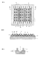
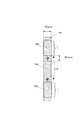
- FIG. 1A shows a plan view of the organic EL display panel described in Patent Document 2.
- FIG. 1B shows a cross-sectional view taken along line III of the organic EL display panel shown in FIG. 1A.
- FIG. 1C is a partially enlarged view of FIG. 1B.
- the organic EL display panel has a glass substrate 1, a first electrode layer 2, a first bank 4, a second bank 3, a hole injection layer 5, and an organic light emitting layer 6. .
- the first bank 4 and the second bank 3 are made of resin.
- the first bank 4 defines a linear area 40. In the linear region 40, organic EL elements are arranged in one row.
- the linear region 40 defines a linear organic light emitting layer 6.
- the second bank 3 defines a pixel area 30.
- the pixel region 30 defines a region of the hole injection layer 5.
- the organic light emitting layer is formed over a plurality of pixel regions (organic EL elements) to make the film thickness in the line direction of the organic light emitting layer uniform. Can. Therefore, the organic light emitting layer 6 is also formed on the second bank 3.
- the bank has a two-layer structure, the upper layer bank is lyophobic, and the lower layer bank is lyophilic so that the material liquid of the functional layer is sufficiently wet and spread within the region defined by the bank.
- the lower layer bank is made lyophilic by adopting a lyophilic material such as an inorganic substance (SiO 2 ) as the material of the lower layer bank.
- JP, 2006-86128 A U.S. Pat. No. 7,091,660 Japanese Patent Application Publication No. 2006-41027 Unexamined-Japanese-Patent No. 2006-286309 JP, 2006-305331, A JP, 2006-71872, A Unexamined-Japanese-Patent No. 11-329741 JP 2007-44582 A JP 2005-222776 A JP, 2006-294446, A
- the ink containing the organic EL material coated on the second bank may be repelled by the second bank. . If the ink is repelled by the second bank, an organic light emitting layer having a uniform film thickness can not be formed. Therefore, the wettability of the upper surface of the second bank is required to be high.
- the first bank needs to define an ink containing the organic EL material to be applied and formed, the wettability of the first bank is required to be low. As described above, when forming a line-shaped organic light emitting layer across a plurality of organic EL elements, the wettability of the first bank needs to be lower than the wettability of the second bank.
- Patent Document 2 disclosing the organic EL display panel of FIGS. 1A to 1C did not disclose a specific means for making the wettability of the first bank lower than the wettability of the second bank.
- the step difference X between the second bank 3 and the hole injection layer 5 is large.
- the second bank defines the hole injection layer formed by the coating method, it is required to have a certain height. For this reason, the line-shaped area
- the second bank 3 it is also conceivable to omit the second bank 3 if the hole injection layer formed by the coating method is a hole injection layer formed by a thin film formation method or the hole injection layer is omitted. However, if the second bank 3 defining the pixel area 30 is omitted, the unevenness in the line-like area 40 may become more noticeable due to the step caused by the difference between the surface of the pixel electrode or the hole injection layer and the surface of the substrate. There is.
- An object of the present invention is to provide an organic EL display panel having a uniform light emitting layer formed in a line shape, a high luminous efficiency, and a long life.
- the first of the present invention relates to the organic EL display panel shown below.
- a substrate a line-like first bank disposed on the substrate and defining a line-like area, and a second bank defining two or more pixel areas arrayed in the line-like area
- a pixel electrode disposed in the pixel region, a line-shaped organic layer disposed in the line region and formed on the pixel region and the second bank by a coating method, and the organic layer.
- An organic EL display panel including a counter electrode disposed, wherein the height of the first bank is higher than the height of the second bank, and the material of the first bank and the second bank is a resin
- the organic EL display panel wherein the contact angle of anisole at the top of the first bank is 30 ° to 60 °, and the contact angle of anisole at the top of the second bank is 5 ° to 30 °.
- the bottom surface of the organic layer is in contact with the pixel electrode, and the height of the second bank from the surface of the pixel electrode is ⁇ 0.1 to +0.4 ⁇ m, [1] or [2] ]
- the organic electroluminescent display panel as described in. [4] It further has a hole injection layer disposed on the pixel electrode and independent for each of the pixel regions, The organic EL display panel according to [1] or [2], wherein a bottom surface of the organic layer is in contact with the hole injection layer.
- the hole injection layer includes an oxide of a transition metal, and the height of the second bank from the surface of the hole injection layer is ⁇ 0.1 to +0.4 ⁇ m, [4]
- the second of the present invention relates to a method of manufacturing an organic EL display panel described below.
- a step of preparing a substrate on which pixel electrodes are arranged, a first linear bank defining a linear region on the substrate, and two or more pixel regions arranged in the linear region Forming a second bank to define a second bank, applying a material liquid containing an organic EL material to the linear region to form a linear organic layer, and forming a counter electrode on the organic layer.
- the method for manufacturing an organic EL display panel wherein the contact angle of anisole is 30 ° to 60 °, and the contact angle of anisole at the top of the second bank is 5 ° to 30 °.
- the step of patterning the resin film includes the step of forming a photosensitive resin film A containing the material of the second bank on the substrate, and the material of the first bank on the photosensitive resin film A Forming a photosensitive resin film B having a sensitivity different from that of the photosensitive resin film A, exposing the photosensitive resin film A and the photosensitive resin film B through masks having different transmittances, And a step of developing the organic EL display panel according to [12].
- the step of patterning the resin film includes the step of forming a photosensitive resin film containing a fluorine compound on the substrate, and the photosensitive resin film containing the fluorine compound through a halftone mask having different transmittances. And exposing and developing the organic EL display panel according to [12].
- the wettability in the application area is high and the application area is flat, so it is possible to provide an organic EL display panel having an organic layer with a uniform film thickness.
- FIG. 1 Top view and sectional view of a conventional organic EL display panel
- FIG. 2 The figure which shows the manufacturing method of the organic electroluminescent display panel of this invention.
- Figure showing an example of a method of producing the first bank and the second bank The figure which shows the organic electroluminescent display panel of this invention
- Cross-sectional view of an organic EL element included in the organic EL display panel of Embodiment 1 Cross-sectional view of an organic EL element included in the organic EL display panel of Embodiment 2
- FIG. 7 is a diagram showing a method of manufacturing the organic EL display panel of Embodiment 2 Top view of organic EL display panel of Embodiment 3
- the organic EL display panel of the present invention has organic EL elements arranged in a matrix on a substrate.
- Each organic EL element has a pixel electrode, an organic layer disposed on the pixel electrode, and a counter electrode disposed on the organic layer.
- the organic layer is formed by a coating method. More specifically, the organic EL display panel of the present invention is defined by 1) a substrate, 2) a pixel electrode, 3) a first bank and a second bank disposed on the substrate, and 4) a first bank. And 5) a counter electrode provided on the organic layer.
- the organic EL display panel of the present invention may be either a passive matrix type in which pixel electrodes are arranged in a line or an active matrix type in which pixel electrodes are arranged independently for each organic EL element, and a bottom emission type
- any of top emission type may be used.
- each component of the organic EL display panel of the present invention will be described.
- the substrate of the organic EL display panel of the present invention differs depending on whether it is a bottom emission type or a top emission type.
- the substrate in the case of a bottom emission type, the substrate is required to be transparent. Therefore, in the case of the bottom emission type, the material of the substrate may be glass, transparent resin or the like.
- the substrate in the case of the top emission type, the substrate does not have to be transparent. Therefore, in the case of top emission type, the substrate may be an insulator.
- the substrate incorporates a thin film transistor (drive TFT) for driving the organic EL element.
- the source electrode or drain electrode of the TFT incorporated in the substrate is connected to a pixel electrode described later (see FIG. 7A).
- Pixel Electrode The pixel electrode is a conductive member disposed on the substrate.
- the pixel electrode usually functions as an anode but can also function as a cathode.
- the pixel electrode is disposed in each pixel region described later.
- the organic EL display panel is a passive matrix type, a plurality of line-shaped pixel electrodes are disposed on the substrate.
- the line-shaped pixel electrodes are preferably parallel to one another.
- the organic EL display panel is an active matrix type, the pixel electrodes are disposed independently for each organic EL element.
- the pixel electrode is required to be a transparent electrode
- examples of the material of the pixel electrode include ITO (indium tin oxide), IZO (indium zinc oxide), ZnO (oxide oxide) Zinc and the like.
- an example of the material of the pixel electrode is an alloy containing silver, more specifically silver-palladium-copper alloy (also referred to as APC) And aluminum-based alloys such as silver-ruthenium-gold alloy (also referred to as ARA), MoCr (molybdenum chromium), NiCr (nickel chromium), aluminum-neodymium alloy (also referred to as Al-Nd), and the like. Further, an ITO film and an IZO film (Indium Zinc Oxide) may be disposed on the surface of the reflective pixel electrode.
- a hole injection layer may be disposed on the pixel electrode.
- the hole injection layer is a layer having a function of assisting the injection of holes from the pixel electrode to the organic layer described later. For this reason, the hole injection layer is disposed between the pixel electrode and the organic layer (see FIGS. 7A and 8B).
- Materials for the hole injection layer include polyethylenesulfonic acid-doped poly (3,4-ethylenedioxythiophene) (referred to as PEDOT-PSS), its derivatives (such as copolymers), and oxidation of transition metals.
- PEDOT-PSS polyethylenesulfonic acid-doped poly (3,4-ethylenedioxythiophene)
- its derivatives such as copolymers
- oxidation of transition metals oxidation of transition metals.
- the material of the hole injection layer is preferably a transition metal oxide.
- transition metals include tungsten, molybdenum, titanium, vanadium, ruthenium, manganese, chromium, nickel, iridium, APC (silver-palladium-copper alloy), and combinations thereof.
- Preferred hole injection layer materials are tungsten oxide (WOx) or molybdenum oxide (MoOx).
- the thickness of the hole injection layer is typically 10 nm to 100 nm and may be about 50 nm.
- the hole injection layer containing PEDOT-PSS is formed by the coating method, it is necessary to define the region where the hole injection layer containing PEDOT-PSS is to be formed in the second bank described later (Patent Document 2) reference). Therefore, a certain height is required for the second bank, and the unevenness of the application area described later may be large (see FIG. 1C).
- the hole injection layer made of transition metal oxide can be formed by sputtering, vapor deposition or the like, and does not have to be defined by the second bank. Therefore, when the hole injection layer is formed of a transition metal oxide, the height of the second bank can be made relatively low, and the unevenness in the application area can be reduced to flatten the application area. it can.
- the hole injection layer may be omitted as long as holes can be efficiently injected from the pixel electrode to the organic layer.
- the organic layer is disposed directly on the pixel electrode.
- an organic layer is disposed on a hole injection layer containing PEDOT-PSS.
- First Bank and Second Bank are barriers disposed on a substrate.
- the materials of the first and second banks include a resin.
- the first bank is a barrier disposed on a substrate that defines a region to which an organic layer described later is to be applied.
- a plurality of first banks are formed in a line on the substrate, and a line area is defined on the substrate (see FIG. 6A).
- An organic layer described later is applied to the linear region.
- a linear area defined by the linear bank (first bank) will be referred to as a "coating area”.
- Pixel regions are arranged in a line in one application region defined by the first bank (see FIG. 6A).
- the pixel area means an area occupied by one organic EL element.
- the linear first banks are preferably parallel to one another.
- the height of the first bank from the surface of the substrate is preferably 0.5 to 3 ⁇ m, and particularly preferably 0.8 ⁇ m to 1.2 ⁇ m.
- all the organic EL elements share one counter electrode, but if the bank height is more than 3 ⁇ m, there is a risk that the counter electrodes may be divided by the bank. There is a risk that the counter electrode shared by all the organic EL elements can not be formed. Also, if the height of the bank is less than 0.5 ⁇ m, there is a risk that the ink applied in the area defined by the bank may leak from the bank.
- the shape of the first bank is preferably forward tapered.
- the forward tapered shape means that the barrier surface of the bank is oblique, and the area of the bottom of the bank is larger than the area of the top of the bank (see FIG. 7A).
- the taper angle is preferably 20 to 80 °, particularly preferably 30 to 45 °.
- the material of the first bank is not particularly limited as long as it is a resin, but is preferably a fluorine-containing resin.
- the fluorine compound contained in the fluorine-containing resin include fluorinated resins such as vinylidene fluoride, vinyl fluoride, ethylene trifluoride, and copolymers of these, and the like.
- the resin contained in the fluorine-containing resin include phenol-novolak resin, polyvinyl phenol resin, acrylic resin, methacrylic resin, and a combination thereof.
- the first bank defines the area to which the ink containing the material of the organic layer is applied as described above, and prevents the ink from leaking out. For this reason, the wettability of the upper surface of the first bank is low.
- the term "low wettability" means that the contact angle of an organic solvent such as anisole or cyclohexylbenzene is 30 ° to 60 °.
- the upper surface of the bank means a surface including the top of the bank.
- the wettability of the bottom of the first bank is preferably higher than the wettability of the top of the first bank.
- the upper surface of the first bank with low wettability suppresses the leakage of the material liquid of the organic layer.
- the high wettability of the lower part of the first bank ensures that the material liquid of the functional layer is applied to the entire area defined by the first bank, that is, to the tangent line between the first bank and the relevant area. .
- the wettability in the bank is mainly determined by the concentration of fluorine atoms. Therefore, in order to lower the wettability of the top surface of the bank and increase the wettability of the bottom surface of the bank, the fluorine concentration of the top surface of the bank may be increased and the fluorine concentration of the bottom surface of the bank may be decreased.
- the fluorine atom concentration at the top of the first bank is preferably 4 to 10 atom%
- the fluorine concentration at the bottom of the first bank is preferably 0 to 3 atom%.
- the fluorine atom concentration can be measured by an X-ray photoelectron spectrometer (also referred to as XPS or ESCA).
- An example of an X-ray photoelectron spectrometer is PHI Quantera SXM (manufactured by ULVAC PHI).
- a bank having a high fluorine concentration on the top surface and a low fluorine concentration on the bottom surface can be formed by baking (baking treatment) a film of a fluorine-containing resin patterned in a desired shape.
- Table 1 is a graph showing the relationship between the thickness (height) of the baked fluorine-containing resin and the concentration of fluorine on the surface of the fluorine-containing resin film and the contact angles of water and anisole on the surface of the fluorine-containing resin film. .
- the contact angles of water and anisole were measured using an automatic liquid crystal glass cleaning and processing inspection device manufactured by Kyowa Interface Science.
- the thicker (higher) the fluorine-containing resin film the higher the fluorine concentration on the surface of the fluorine-containing resin film.
- the wettability of the fluorine-containing resin is mainly determined by the concentration of the fluorine atom, the higher the fluorine concentration, the larger the contact angle of water and the contact angle of the organic solvent (the wettability decreases).
- the fluorine atom concentration at the surface of the fluorine-containing resin film having a thickness of 1 ⁇ m is 7.5 atom%
- the water contact angle at the surface of the fluorine-containing resin film is 81.2 °
- the surface at the surface of the fluorine-containing resin film The contact angle of anisole is 45.5 °.
- the fluorine atom concentration on the surface of the fluorine-containing resin film having a thickness of 0.3 ⁇ m is 3.0 atom%
- the water contact angle on the surface of the fluorine-containing resin film is 64.6 °
- the fluorine-containing resin film The contact angle of anisole on the surface of is 28.4 °.
- the shape of the bank made of the fluorine-containing resin into a forward tapered shape, a gradient of the fluorine concentration can be generated along the height direction of the first bank.
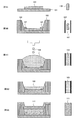
- FIG. 2 is a cross-sectional view of the organic EL element having the bank 105 in the forward tapered shape.
- a gradient occurs in the height of the bank on the wall surface. That is, as shown in FIG. 2, the heights of the banks become smaller in the order of 5a, 5b, 5c.
- the density of the fluorine component on the top of the low bank is low; the density of the fluorine component on the top of the high bank is high. Therefore, the fluorine concentration in the portion 5a (the bank is high) is relatively high and the fluorine concentration in the portion 5c (the bank is low) of the forward tapered banks 105 shown in FIG. It becomes relatively low. Therefore, the fluorine concentration in the bank 105 becomes lower in the order of 5a, 5b and 5c.
- reference numeral 101 denotes a substrate
- reference numeral 103 denotes an electrode.
- the shape of the first bank made of the fluorine-containing resin into a forward tapered shape, it is possible to generate a gradient of the fluorine concentration in the height direction of the first bank. Further, by generating a fluorine concentration gradient in the height direction of the first bank, it is possible to obtain a wettability gradient along the bank height direction.
- the material solution of the organic layer in the area defined by the first bank having the wettability gradient in the height direction the organic layer can be formed correctly and the organic layer having a uniform film thickness is formed. can do.
- the first bank may define an application region and also function as a counter electrode separator.
- the counter electrode separator is a member for separating a counter electrode (described later), and for example, the counter electrode formed on an organic layer described later by vapor deposition is divided into line-shaped application areas.
- the second bank is disposed on the substrate, defines two or more pixel areas in the application area (see FIG. 6), and has a function to flatten the inside of the application area.
- the organic layer formed by the coating method is also disposed on the second bank, the height of the second bank is smaller than that of the first bank. The height of the second bank will be described later.
- the wettability of the upper surface of the second bank is preferably high.
- the upper surface of the second bank is required to have affinity for the material liquid of the organic layer. It is.
- high wettability means that the contact angle of an organic solvent such as anisole or cyclohexylbenzene is 5 ° to 30 °, and the contact angle of water is 30 ° to 90 °.
- the present invention is characterized in that although the materials of the first bank and the second bank are both resin, the wettability of the first bank and the second bank is different. Since the wettability of the first bank and the second bank is different, an organic layer having a uniform film thickness can be formed in a line by the coating method.
- the composition of the resin contained in the first bank and the composition of the resin contained in the second bank may be changed.
- changing the composition of the resin means changing the molecular structure of the monomer of the resin, changing the ratio of monomers, changing the amount of additives, and the like.
- the material of the first bank and the material of the second bank may be different, and B) In some cases, the material of the first bank and the material of the second bank may be the same.
- the material of the second bank is a resin having higher wettability than the first bank Should be used.
- highly wettable resins include polyimide resins and acrylic resins that do not contain fluorine.
- both the materials of the first bank and the second bank may be made of a fluorine-containing resin.
- the wettability of the fluorine-containing resin depends on the thickness (height) of the fluorine-containing resin (see Table 1). Also, as described above, the height of the second bank is lower than the height of the first bank. Therefore, even if the materials of the first and second banks are both fluorine-containing resins, the wettability of the upper surface of the first bank can be lowered and the wettability of the upper surface of the second bank can be increased.
- the fluorine concentration at the top of the second bank is preferably 1 to 4 atom% when both the materials of the first bank and the second bank are fluorine-containing resin.
- the height of the second bank differs depending on the material of the layer in contact with the bottom surface of the organic layer described below (hereinafter, also simply referred to as "the lower layer of the organic layer").
- the lower layer of the organic layer is i) a pixel electrode, ii) a hole injection layer made of transition metal oxide, and iii) a hole injection layer containing PEDOT-PSS.
- the height of the second bank will be described separately for each case.
- the height from the surface of the pixel electrode of the second bank is preferably ⁇ 0.1 to +0.4 ⁇ m, More preferably, it is about 0 ⁇ m.
- the second bank does not have to define the layer formed by the coating method, so the height from the surface of the pixel electrode of the second bank is relatively low. can do. Thereby, the inside of the application region can be made flat, and the film thickness of the organic layer can be made more uniform.
- the second bank since it is not necessary to define the layer formed by the application method, the second bank may be omitted.
- the unevenness in the linear region 40 may be remarkable due to the difference in level between the surface of the pixel electrode or the hole injection layer and the surface of the substrate.
- the lower layer of the organic layer is a hole injection layer composed of a transition metal oxide (see Embodiment 1)
- the height from the surface of the hole injection layer made of a transition metal oxide of the second bank is -0.1 to +0.4 ⁇ m Is preferably, and more preferably about 0 ⁇ m.
- the second bank does not have to define the layer formed by the coating method.
- the height from the surface of the hole injection layer made of oxide can be made relatively low. Thereby, the inside of the application region can be made flat, and the film thickness of the organic layer can be made more uniform.
- the lower layer of the organic layer is a hole injection layer containing PEDOT-PSS (see Embodiment 2)
- the height from the surface of the pixel electrode of the second bank is preferably 0.1 to 0.5 ⁇ m.
- the hole injection layer containing PEDOT-PSS is formed by a coating method. Therefore, when the lower layer of the organic layer is a hole injection layer containing PEDOT-PSS, the second bank defines a region to which the material liquid of the hole injection layer (a solution containing PEDOT-PSS and water) is applied. Is required. For this reason, the height from the surface of the hole injection layer including PEDOT-PSS of the second bank is increased compared to i) and ii).
- the wettability of the upper surface of the second bank is the same as in the first bank. And lower than the wettability of the upper surface of the second bank.
- the second bank has a wettability gradient along the height direction of the bank. Since the second bank has a wettability gradient along the bank height direction, it is possible to accurately form a hole injection layer including PEDOT-PSS having a uniform film thickness.
- the organic layer is a layer including at least an organic light emitting layer and disposed on the pixel electrode.
- the organic layer is formed by applying the material solution of the organic layer to the linear application region defined by the first bank.
- the material solution of the organic layer in which the material of the organic layer is dissolved in an organic solvent such as anisole or cyclobenzene
- a coating method such as inkjet
- damage to other materials is easy It is because an organic layer can be formed without giving.
- the organic layer is formed in a line shape (across a plurality of organic EL elements) in the application region defined by the first bank described later. Therefore, the organic layer is disposed not only on the pixel region but also on the second bank.
- the organic EL material contained in the organic light emitting layer may be a polymer or a low molecule as long as the organic light emitting layer can be formed by a coating method.
- the organic EL material contained in the organic light emitting layer is preferably a high molecular weight organic EL material, since the organic light emitting layer containing the high molecular weight organic EL material is easily formed by a coating method.
- polymer organic EL materials examples include polyphenylene vinylene and its derivative, polyacetylene (Poly acetylene) and its derivative, polyphenylene (Poly phenylene and its derivative), poly para phenylene ethylene (Poly para phenylene ethylene) and its derivative, poly 3 And poly-hexylthiophene (P3HT) and derivatives thereof, and polyfluorene (PF) and derivatives thereof.
- examples of low molecular weight organic EL materials include tris (8-quinolinolato) aluminum and the like.
- the organic EL material is appropriately selected such that desired color development (red R, green G, blue B) is generated from each pixel.
- desired color development red R, green G, blue B
- a green pixel is disposed next to a red pixel
- a blue pixel is disposed next to a green pixel
- a red pixel is disposed next to a blue pixel.
- the thickness of the organic light emitting layer is preferably about 50 to 150 nm (eg, 60 nm).
- the organic layer may further have an electron block layer, an electron transport layer, and the like.
- the electron blocking layer has a role of blocking the penetration of electrons into the hole injection layer and a role of efficiently transporting holes to the organic light emitting layer, and is a layer made of, for example, a polyaniline-based material.
- the thickness of the electron blocking layer is usually 5 nm or more and 100 nm or less, preferably 10 nm or more and 50 nm or less (for example, about 20 nm).
- the electron blocking layer may be omitted as long as holes can be efficiently transported to the organic light emitting layer.
- the counter electrode is a conductive member disposed on the organic layer.
- the counter electrode usually functions as a cathode but can also function as an anode.
- the material of the counter electrode differs depending on whether it is bottom emission type or top emission type.
- the material of the counter electrode is preferably an ITO electrode, an IZO electrode, or the like.
- the material of the counter electrode may be Ba, Al, WOx or the like.
- an organic buffer layer may be disposed between the organic light emitting layer and the counter electrode layer.
- the counter electrode does not have to be transparent. Therefore, the material of the counter electrode may be arbitrary, and includes, for example, barium (Ba), barium oxide (BaO), aluminum (Al) and the like.
- the counter electrode may be formed on the electron injection layer or the organic light emitting layer disposed in each pixel area, but is usually formed so as to cover a plurality of application areas.
- the counter electrode is usually formed by a vapor deposition method, and may not necessarily be separated for each application region. That is, if the pixel electrode is controlled independently for each organic EL element as in the active matrix type, the TFT element for driving the organic EL element is independent, so the counter electrode is shared by a plurality of application regions. be able to.
- an electron injection layer made of barium (Ba), lithium fluoride (LiF) or the like may be disposed between the counter electrode and the organic layer.
- a cover material may be provided on the surface of the organic EL display panel of the present invention on which the counter electrode is further formed for sealing.
- the cover material prevents moisture and oxygen from entering.
- the present invention since the wettability in the application region is high and flat, it is possible to provide an organic EL display panel having an organic layer with a uniform film thickness.
- the organic electroluminescent display panel of this invention may be manufactured by arbitrary methods, as long as the effect of this invention is not impaired.
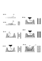
- An example of a preferred manufacturing method is 1) a first step (FIG. 3A) of preparing a substrate on which a pixel electrode is disposed; 2) a second step (FIG. 3B) of forming a first bank and a second bank on the substrate; 3) Third step (FIGS. 3C and 3D) of forming a line-shaped organic layer in the application area; 4) forming a counter electrode on the organic layer (FIG. 3E).
- FIG. 3A shows the first step.
- the substrate 101 on which the pixel electrode 103 is disposed is prepared.
- the substrate 101 may incorporate a thin film transistor (drive TFT).
- the substrate may be prepared by forming a passivation film and a planarizing film on the surface on which the drive TFT is formed.
- the pixel electrode 103 is formed, for example, by forming a film of an electrode material on the substrate 101 by sputtering or the like, and etching and patterning.
- a hole injection layer formed of a transition metal oxide may be formed on the pixel electrode 103.
- FIG. 3B shows the second step.
- the first bank 105 and the second bank 107 are formed on the substrate 101.
- the first bank 105 defines a linear coating area
- the second bank 107 defines a pixel area.
- the step of forming the first bank 105 and the second bank 107 includes the steps of patterning the resin film and baking the patterned resin film.
- the resin film can be patterned by photolithography.
- the resin film may be patterned by intaglio printing or the like. If formed by intaglio printing or the like, other materials (such as pixel electrodes) are less likely to be damaged.
- the resin film may be patterned by letterpress printing.
- Step i (FIG. 4A) of forming a photosensitive resin film A on a substrate; ii) forming a photosensitive resin film B on the photosensitive resin film A (FIG. 4B); iii) exposing and developing the photosensitive resin film A and the photosensitive resin film B through halftone masks having different transmittances, as shown in FIG. 4C and FIG. 4D.
- FIG. 4A shows step i.
- a photosensitive resin film A 104 is formed on the substrate 101.
- the photosensitive resin film A 104 contains the material of the second bank 107.
- the thickness of the photosensitive resin film A104 is preferably 0.1 to 0.5 ⁇ m.
- the photosensitive resin composition may be applied onto the substrate 101 by spin coating or the like, and the applied film may be dried. Although the drying conditions are not particularly limited, it may be left at 80 ° C. for 2 to 3 minutes.
- FIG. 4B shows step ii.
- a photosensitive resin film B106 is formed on the photosensitive resin film A104.
- the photosensitive resin film B 106 contains the material of the first bank 105.
- the thickness of the photosensitive resin film B106 is preferably 0.5 to 3 ⁇ m.
- the sensitivity of the photosensitive resin film B106 is different from the sensitivity of the photosensitive resin film A. Specifically, when the photosensitive resin film A104 and the photosensitive resin film B106 are negative photosensitive resin films, the sensitivity of the photosensitive resin film B106 may be weaker than the sensitivity of the photosensitive resin film A104. . On the other hand, when the photosensitive resin film A104 and the photosensitive resin film B106 are positive photosensitive resin films, the sensitivity of the photosensitive resin film B106 may be made stronger than the sensitivity of the photosensitive resin film A104.
- Figures 4C and 4C 'and Figure 4D show step iii.
- step iii the photosensitive resin film A 104 and the photosensitive resin film B 106 are exposed through the halftone mask 110 having different transmittances.
- FIG. 4C shows the case where the photosensitive resin film A104 and the photosensitive resin film B106 are negative photosensitive resin films.
- the area for exposing the pixel electrode 103 is not exposed; the area for forming the second bank 107 is exposed through the halftone mask; the area for forming the first bank 105 is exposed without the mask 110. Just do it.
- both the photosensitive resin film B106 and the photosensitive resin film A104 are removed by the developing process, and the pixel electrode 103 is exposed (FIG. 4D).
- the photosensitive resin film B106 and the photosensitive resin film A104 are also cured in the area exposed without the mask 110, the first bank 105 is formed by the developing process (FIG. 4D).
- the photosensitive resin film A104 having high sensitivity cures, and the photosensitive resin film B106 having low sensitivity is not cured.
- the resin film B 106 is removed to form a second bank 107 (FIG. 4D).
- FIG. 4C shows the case where photosensitive resin film A104 and photosensitive resin film B106 are positive photosensitive resin films.
- the area where the pixel electrode 103 is exposed is exposed without passing through the mask 110; the area where the second bank 107 is to be formed is exposed through the halftone mask; the area where the first bank 105 is to be formed is not exposed. Just do it.
- the photosensitive resin film B106 and the photosensitive resin film 104 are also removed by the development step.
- the pixel electrode 103 is exposed (FIG. 4D).
- the photosensitive resin film remains cured, so that the first bank 105 is formed by the developing process (FIG. 4D).
- the solubility of only the photosensitive resin film B106 with high sensitivity is increased, and the photosensitive resin film A104 with low sensitivity is still cured. Only the photosensitive resin film B106 is removed to form a second bank 107 (FIG. 4D).
- the photosensitive resin film A containing the material of the second bank is formed; the photosensitive resin film B containing the material of the first bank is formed thereon; the sensitivity of the photosensitive resin film A and the photosensitive property
- the resin film B is made different in sensitivity, it is possible to accurately pattern the first bank and the second bank having different shapes in one developing step.
- the step of patterning the resin film by photolithography is as shown in FIGS. 5A to 5C, i) forming a photosensitive resin film 104 'on a substrate (FIG. 5A); ii) Step ii (FIGS. 5B and 5C) of exposing and developing the photosensitive resin film 104 ′ through the halftone mask 110 having different transmittances.
- the photosensitive resin film to be formed is a single layer. Thereby, it is possible to simultaneously pattern the first and second banks having different shapes from the same resin material. Further, in the method shown in FIG. 5, since the first bank 105 and the second bank 107 are made of the same resin material, the material of the first bank 105 and the second bank 107 is a fluorine-containing resin. Is preferred.
- the patterned resin film is baked to form a first bank and a second bank.
- the material of the bank is a fluorine-containing resin
- the baking treatment can cause the fluorine component of the fluorine compound resin contained in the film to float on the film surface.
- a bank having a desired wettable surface is formed.
- the wettability of the bank can be varied according to the height of the bank.
- hole injection is performed by applying a solution containing PEDOT-PSS and water on the pixel electrode in the area defined by the second bank.
- a layer may be formed.
- FIGS 3C and 3D show the third step.
- the linear organic layer 109 is formed in the application region.
- the line-shaped organic layer 109 is a material liquid 108 of an organic layer applied by using an inkjet or the like in a line-shaped application region defined by the first bank 105 (a material of the organic layer and an organic such as anisole or cyclobenzene) It is formed by drying the ink containing the solvent. Since the wettability of the upper surface of the second bank 107 is low as described above, the material liquid 108 of the organic layer can be applied in the application area without being repelled by the second bank 107.
- the unevenness in the application region is small and the organic film having a more uniform film thickness.
- the layer 109 can be formed.
- FIG. 3E shows the fourth step.
- the counter electrode 111 is formed on the organic layer 109.
- the counter electrode 111 may be formed, for example, using a vapor deposition method or a sputtering method.
- an electron injecting layer may be formed over the organic layer 109 by evaporation, sputtering, or the like before the formation of the counter electrode 111.
- an organic EL having an organic layer with a uniform film thickness can be more simply. Display panels can be manufactured.
- Embodiment 1 In the first embodiment, a top emission type organic EL display panel will be described. Moreover, the organic EL display panel of Embodiment 1 is an active matrix type.
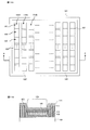
- FIG. 6A is a plan view of the active matrix organic EL display panel according to Embodiment 1 in which the counter electrode and the organic light emitting layer are omitted.
- FIG. 6B is a perspective view of the organic EL display panel shown in FIG. 6A.
- a plurality of line-shaped first banks 105 are disposed on the substrate 101.
- the first bank 105 defines a coating area 119.
- the application area 119 is classified into an application area 119R emitting red light; an application area 119G emitting green light; and an application area 119B emitting blue light, which are arranged in order.
- a second bank 107 lower than the first bank 105 is disposed on the substrate 101.
- the second bank 107 defines a plurality of pixel areas 120 arranged in the application area 119.
- the end in the long axis direction of the application area 119 is not defined by the bank.
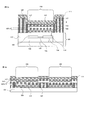
- FIG. 7A is a sectional view taken along the line AA of the organic EL element included in the organic EL display panel of Embodiment 1.
- FIG. 7B is a cross-sectional view of the organic EL element taken along the line BB.
- FIG. 7B shows a cross-sectional view of two organic EL elements.
- the organic EL device includes the substrate 101, the pixel electrode 103, the hole injection layer 113, the linear electron block layer 115, the linear organic light emitting layer 117, the first bank 105, The second bank 107 and the counter electrode 111 are provided.
- the substrate 101 incorporates a thin film transistor (TFT). Control of light emission of the organic light emitting layer 117 is ON / OFF or the like by the TFT incorporated in the substrate 101.
- the TFT contained in the substrate 101 includes a gate electrode 131, a gate insulating layer 132, a source electrode 133, a drain electrode 134, a semiconductor layer 135, a contact hole 136, and a planarization film 137.
- the pixel electrode 103 is connected to the drain electrode 134 by the contact hole 136.
- the pixel electrode 103 is preferably a reflective pixel electrode made of an APC film or the like with a thickness of 100 to 200 nm.
- the counter electrode 111 is preferably an ITO film.
- the hole injection layer 113 is made of a transition metal oxide (for example, tungsten oxide).
- the hole injection layer 113 may be formed by depositing a layer formed of a transition metal oxide by sputtering or the like, and patterning the deposited layer by etching.
- the linear electron blocking layer 115 is disposed on the hole injection layer 113 and the second bank 107 as shown in FIG. 7B.
- the linear organic light emitting layer 117 is disposed on the linear electron blocking layer 115 as shown in FIG. 7B.
- the first bank 105 defines an arrangement area (application area) of the electron blocking layer 115 and the organic light emitting layer 117. Further, the first bank 105 is in a forward tapered shape. The taper angle ⁇ of the first bank 105 is preferably 20 to 80 °, and more preferably 30 to 45 °.
- the second bank 107 defines the pixel area 120 as described above. In the present embodiment, the height 107 h from the surface of the hole injection layer 113 of the second bank 107 is ⁇ 0.1 to +0.4 ⁇ m.
- the wettability of the upper surface of the first bank 105 is lower than the wettability of the upper surface of the second bank 107.
- the contact angle of anisole at the top of the first bank 105 is 30 ° to 60 °; the contact angle of anisole at the top of the second bank 107 is 5 ° to 30 °.
- the application area is flat because the height from the surface of the hole injection layer of the second bank is relatively low. Also, the wettability of the upper surface of the second bank is high. For this reason, according to the present embodiment, the film thickness of the organic layer (electron block layer) formed by the application method in the application region can be made uniform.
- the hole injection layer is made of a transition metal oxide has been described.
- the hole injection layer includes PEDOT-PSS will be described.
- the organic EL display panel of Embodiment 2 is 1) that the material of the hole injection layer is PEDOT-PSS, and 2) that the positional relationship between the second bank and the hole injection layer is different. Is the same as the organic EL display panel. Therefore, the same components as in the first embodiment will be assigned the same reference numerals and descriptions thereof will be omitted.
- FIG. 6A is a plan view of the active matrix organic EL display panel according to Embodiment 2 in which the counter electrode and the organic light emitting layer are omitted.
- FIG. 6B is a perspective view of the organic EL display panel shown in FIG. 6A.
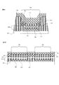
- FIG. 8A is a sectional view taken along the line AA of the organic EL element included in the organic EL display panel of Embodiment 1.
- FIG. 8B is a cross-sectional view of the organic EL element taken along the line BB.
- FIG. 8B shows a cross-sectional view of two organic EL elements.
- the organic EL device includes the substrate 101, the pixel electrode 103, the hole injection layer 113 ′, the linear electron block layer 115, and the linear organic light emitting layer 117. , The first bank 105, the second bank 107, the electron injection layer 118, and the counter electrode 111.
- the second embodiment is the same as the first embodiment except that the material of the hole injection layer is PEDOT-PSS, and the positional relationship between the second bank and the hole injection layer is different. . Therefore, hereinafter, 1) the hole injection layer 113 'and 2) the second bank will be described.
- Hole injection layer 113 ′ includes PEDOT-PSS. As described later, the hole injection layer 113 'is formed by applying an aqueous solution containing PEDOT-PSS into the area defined by the second bank 107. As described above, the hole injection layer 113 'formed by the application method is disposed independently for each pixel region 120 (organic EL element).
- the hole injection layer 113 ′ including PEDOT-PSS is formed by a coating method in the same manner as the linear organic layer (electron block layer 115, organic light emitting layer 117). Therefore, it is also conceivable that the hole injection layer 113 'is also formed in a line shape in the application region as in the organic layer. However, the hole injection layer 113 ′ is preferably disposed independently for each pixel region 120. Hereinafter, the merit of arranging the hole injection layer 113 ′ independently for each pixel region 120 will be described with reference to FIG.
- FIG. 9 shows a partially enlarged view of the application area of the organic EL display panel.
- the width of the pixel electrode 103 of each organic EL element is 70 ⁇ m, and the distance between adjacent pixel electrodes is 55 ⁇ m.
- the hole injection layer 113 is arranged in a line across the three organic EL elements a, b and c.
- Equation 1 shows the relationship between the resistance between the pixel electrodes and the specific resistance of the hole injection layer (PEDOT-PSS), the distance between adjacent pixel electrodes, and the cross-sectional area of the hole injection layer.
- PEDOT-PSS hole injection layer
- the resistance R is 1.2 ⁇ 10 5 ⁇ from Expression 1.
- the current density in the organic EL element b is 10 mA / cm 2 .
- the current flowing to the adjacent elements a and c of the organic EL element b is (5 ⁇ 10 ⁇ 2 / ⁇ ) mA.
- the current density in the organic EL elements a and c at this time is (3.3 ⁇ 10 2 / ⁇ ) mA / cm 2 .
- the specific resistance of the hole injection layer made of PEDOT-PSS can be increased by increasing the doped amount of polystyrene sulfonic acid (PSS), but when the doped amount of polystyrene sulfonic acid is increased, The lifetime (brightness half time) may be shortened, and the performance of the organic EL display panel may be degraded. Therefore, the hole injection layer having the specific resistance as described above may lower the performance of the organic EL display panel.
- PSS polystyrene sulfonic acid
- the contrast ratio is determined by the specific resistance of the organic layer (electron block layer, organic light emitting layer) disposed across the plurality of organic EL elements. As it is determined, it is not necessary to increase the specific resistance of the hole injection layer. Further, since the specific resistance of the organic layer is generally high, there is little possibility that the contrast ratio is lowered even if the organic layer is formed across a plurality of organic EL elements.
- Second bank 107 is a barrier which defines the pixel area 120 in the application area 119 and defines the arrangement area of the hole injection layer 113 ′ formed by the application method.
- the wettability of the upper surface of the second bank 107 is higher than the wettability of the upper surface of the first bank 105.
- the second bank 107 defines the arrangement region of the hole injection layer 113 ′ formed by the coating method, the upper surface of the second bank 107 is formed of the material liquid of the hole injection layer 113 ′ It is required to exhibit liquid repellency for an aqueous solution containing PEDOT-PSS. Since the aqueous solution has relatively high surface tension, it can be defined even in the second bank with high wettability.
- the linear organic layer (electron block layer 115) is formed by the coating method on the second bank 107, the upper surface of the second bank 107 is formed of the material liquid of the electron block layer 115 (electron block layer). It is required to exhibit lyophilicity for a solution containing the material of 115 and an organic solvent such as anisole.
- the contact angle of anisole on the top surface of the second bank is 5 ° to 30 °, and the contact angle of water is 30 to 90 °. If the wettability of the second bank 107 is higher than this, the material solution of the hole injection layer 113 ′ can not be defined. On the other hand, when the wettability of the second bank 107 is lower than this, the material liquid of the electron block layer 115 is repelled by the second bank 107, and an electron block layer having a uniform film thickness can not be formed.
- the height 107 h from the surface of the pixel electrode 103 of the second bank 107 is 0.1 to 0.5 ⁇ m.
- the manufacturing method of the organic EL display panel of Embodiment 2 is 1) a first step of preparing the substrate 101 (FIG. 10A), 2) Second step of arranging the pixel electrode 103 on the substrate 101 (FIG. 10B) 3) forming a linear first bank 105 for defining the application area and a second step for forming a second bank 107 for defining the pixel area (FIG. 10C); 4) forming a hole injection layer in the pixel area defined by the second bank 107 (FIG. 10D); 5) a fifth step (FIG. 10E) of forming a linear electron block layer in the linear application region defined by the first bank 105; 6) a sixth step (FIG. 10F) of forming a linear organic light emitting layer on the electron blocking layer in the application region; 7) A seventh step (FIG. 10G) of forming a counter electrode on the organic light emitting layer.
- Each step will be described below.
- the substrate 101 is prepared.
- the pixel electrode 103 is disposed on the substrate 101.
- a linear first bank 105 defining the application area 119 and a second bank 107 defining the pixel area 120 are formed.
- the hole injection layer 113 ′ is formed in the pixel region 120 defined by the second bank 107.
- the hole injection layer 113 ′ is a material liquid of the hole injection layer 113 ′ applied by the ink jet method or the like on the pixel electrode 103 in the pixel region 120 defined by the second bank 107 (an ink containing PEDOT-PSS and water ) Is formed by drying.
- the linear electronic block layer 115 is formed in the linear application region 119 defined by the first bank 105.
- the electron blocking layer 115 is formed by drying the material liquid of the electron blocking layer 115 which is applied by an inkjet method or the like in the line-shaped application region 119 defined by the first bank 105.
- the material liquid of the electron block layer 115 can be applied in the application region 119 without being repelled by the second bank 107. it can.
- the linear organic light emitting layer 117 is formed on the electron blocking layer 115 in the application region 119.
- the organic light emitting layer 117 is formed by drying the material liquid of the organic light emitting layer applied on the electron block layer 115 in the application region 119 by an inkjet method or the like.
- the counter electrode 111 is formed on the organic light emitting layer 117.
- the electron injecting layer 118 may be formed on the organic light emitting layer 117 using a vapor deposition method, a sputtering method, or the like before the formation of the counter electrode 117.
- the hole injection layer containing PEDOT-PSS is formed independently for each pixel region, and The electron blocking layer and the organic light emitting layer to be formed can be formed in a line. As a result, it is possible to obtain an organic EL display panel having a long life and a high contrast ratio without crosstalk between pixels.
- Embodiments 1 and 2 an example in which the end in the long axis direction of the application region is not defined has been described.
- an example in which the end in the long axis direction of the application region is also defined by the first bank will be described.
- the second bank is disposed between the pixel region and the first bank (see FIG. 6).
- the pixel region is provided. A mode in which the second bank is not disposed between the first bank and the second bank will be described.
- the organic EL display panel according to the present embodiment has a first bank 105 'that defines the end of the application area, and does not have the second bank 107 between the pixel area 120 and the first bank 105.
- FIG. 11A is a plan view of the active matrix organic EL display panel according to the present embodiment from which the counter electrode and the organic layer are removed.
- the first banks 105, 105 ' define two or more linear application areas 119.
- the longitudinal end of the application area 119 is defined by the first bank 105 '.
- the height of the first bank 105 ′ may be the same as the height of the first bank 105.
- the second bank 107 is not disposed between the pixel area 120 and the first bank 105, and the second bank is only between the pixel areas 120. Will be placed.
- FIG. 11B is a cross-sectional view of the organic EL element included in the organic EL display panel of the present embodiment shown in FIG. 11A. As shown in FIG. 11B, in the AA line sectional view of the organic EL element, there is no second bank, and the pixel region 120 extends to the end of the first bank 105.
- the first bank 105 completely defines the application area 119 where the material layer of the organic light emitting layer is to be applied. This prevents the material solution of the organic light emitting layer from invading the other application region adjacent to the material solution of the organic light emitting layer applied to one application region. For example, the material liquid of the organic light emitting layer to be applied to the application area 119G is prevented from intruding into the adjacent application area 119B. Thereby, a higher quality organic EL display panel can be provided.
- the pixel area can be widened, and the aperture ratio can be improved. Thereby, an organic EL display panel with a high aperture ratio can be provided.
- An APC film with a thickness of 100 to 200 nm was formed by sputtering on a ⁇ 6 inch glass substrate, and etching was performed using a resist as a mask to pattern a reflective pixel electrode. After that, a coating film (thickness: 1.0 ⁇ m) of an acrylic resin containing a photosensitive fluorine compound was formed on the glass substrate on which the reflective pixel electrode was patterned. Next, the coated film is exposed through a halftone mask, and the first bank (height 1.0 ⁇ m) and the second bank (height 0.1 to 0.3 ⁇ m) are patterned and baked (220 ° C., 1 hour was performed to form the first bank and the second bank.
- An ink containing PEDOT-PSS was dropped by an ink jet method on the reflective pixel electrode in the pixel region defined by the second bank and dried to form a hole injection layer (thickness 50 to 100 nm).
- a material liquid of an electron blocking layer containing a polyaniline derivative and anisole was dropped by an ink jet method on the application region defined by the first bank, and dried and fired to form an electron blocking layer (20 to 50 nm in thickness).
- a material solution of an organic light emitting layer containing a polyfluorene derivative and anisole is dropped by an ink jet method on the electron block layer, dried and fired to form an organic light emitting layer (thickness 50 to 150 nm).
- the model of the organic electroluminescent display panel of this invention was produced.
- the electron injection layer and the counter electrode were not produced in this example. That is, the cross-sectional view of the organic EL element in the organic EL display panel of this embodiment is as shown in FIG.
- the film thickness distribution of the organic light emitting layer of the organic EL element 1 in the model of the organic EL display panel formed in this manner was measured along the longitudinal direction of the application region (arrow X direction in FIG. 6A).
- a film thickness distribution was measured using a P-15 stylus type profilometer manufactured by KLA-Tencor.
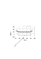
- the graph of FIG. 13 shows the results of the film thickness distribution measurement of the example.
- the vertical axis of the graph of FIG. 13 indicates the thickness of the organic light emitting layer.
- the horizontal axis of the graph of FIG. 13 indicates the measurement position.
- a in the graph of FIG. 13 indicates the length of the pixel area in the X direction.
- the film thickness of the organic light emitting layer in the pixel region was dispersed in the range of ⁇ 3%.
- a model of the organic EL display panel was formed in the same manner as the example except that the height of the second bank was made the same as the height (1.0 ⁇ m) of the first bank. That is, in the comparative example, banks of the same height surround four sides of the pixel area.
- the hole injection layer is disposed independently for each organic EL element, and the electron blocking layer and the organic light emitting layer are formed in a line shape, while in the comparative example, the hole injection layer, the electron Both the block layer and the organic light emitting layer are disposed for each organic EL element.
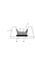
- the organic EL display model of the comparative example has only a bank 17 which defines a pixel area as shown in FIG.
- the organic EL element in the cross-sectional view along the line AA 'in FIG.
- the film thickness distribution of the organic light emitting layer of the organic EL element in the model of the organic EL display panel formed in this manner was measured along the longitudinal direction of the pixel region (arrow X direction in FIG. 14).
- the measuring device used for measuring the film thickness distribution and the measuring conditions are the same as those of the example.
- FIG. 16 shows the result of film thickness distribution measurement.
- the film thickness of the organic light emitting layer in the pixel region was dispersed in the range of ⁇ 31%.
- an organic EL display panel excellent in image characteristics can be provided.
Landscapes
- Engineering & Computer Science (AREA)
- Manufacturing & Machinery (AREA)
- Microelectronics & Electronic Packaging (AREA)
- Electroluminescent Light Sources (AREA)
Abstract
Description
[1]基板と、前記基板上に配置され、ライン状の領域を規定するライン状の第1バンクと、前記ライン状の領域内に配列された2以上の画素領域を規定する第2バンクと、前記画素領域に配置された画素電極と、前記ライン状の領域内に配置され、前記画素領域および前記第2バンク上に塗布法によって形成されたライン状の有機層と、前記有機層上に配置された対向電極と、を含む有機ELディスプレイパネルであって、前記第1バンクの高さは、前記第2バンクの高さよりも高く、前記第1バンクおよび第2バンクの材料は樹脂であり、前記第1バンクの頂点におけるアニソールの接触角は、30°~60°であり、前記第2バンクの頂点におけるアニソールの接触角は、5°~30°である、有機ELディスプレイパネル。
[2]前記第1バンクの基板の前記表面からの高さは0.5~3μmである、[1]に記載の有機ELディスプレイパネル。
[3]前記有機層の底面は、前記画素電極と接触し、前記画素電極の表面からの前記第2バンクの高さは、-0.1~+0.4μmである、[1]または[2]に記載の有機ELディスプレイパネル。
[4]前記画素電極上に配置され、前記画素領域ごとに独立した正孔注入層をさらに有し、
前記有機層の底面は、前記正孔注入層と接触する、[1]または[2]に記載の有機ELディスプレイパネル。
[5]前記正孔注入層は、遷移金属の酸化物を含み、前記正孔注入層の表面からの前記第2バンクの高さは、-0.1~+0.4μmである、[4]に記載の有機ELディスプレイパネル。
[6]前記正孔注入層は、ポリエチレンジオキシチオフェンを含み、前記画素電極の表面からの前記第2バンクの高さは、0.1~0.5μmである、[4]に記載の有機ELディスプレイパネル。
[7]前記第1バンクの材料は、フッ素含有樹脂である、[1]~[6]のいずれか一つに記載の有機ELディスプレイパネル。
[8]前記第1バンクは、前記第1バンクの高さ方向に沿ってフッ素濃度の勾配を有し、前記第1バンクの頂点におけるフッ素濃度は、前記第1バンクの底面におけるフッ素濃度よりも高い、[7]に記載の有機ELディスプレイパネル。
[9]前記第2バンクの材料は、フッ素含有樹脂である、[7]または[8]に記載の有機ELディスプレイパネル。
[10]前記第1バンクの頂点におけるフッ素濃度は、前記第2バンクの頂点におけるフッ素濃度よりも高い、[9]に記載の有機ELディスプレイパネル。
[11]画素電極が配置された基板を準備するステップと、前記基板上にライン状の領域を規定するライン状の第1バンクと、前記ライン状の領域内に配列された2以上の画素領域を規定する第2バンクと、を形成するステップと、前記ライン状の領域に有機EL材料を含む材料液を塗布し、ライン状の有機層を形成するステップと、前記有機層上に対向電極を形成するステップと、を有し、前記第1バンクの高さは、前記第2バンクの高さよりも高く、前記第1バンクおよび第2バンクの材料は樹脂であり、前記第1バンクの頂点におけるアニソールの接触角は、30°~60°であり、前記第2バンクの頂点におけるアニソールの接触角は、5°~30°である、有機ELディスプレイパネルの製造方法。
[12]前記第1バンクおよび前記第2バンクを形成するステップは、前記基板上に、樹脂膜をパターニングするステップと、前記樹脂膜をベークするステップと、を有する、[11]に記載の有機ELディスプレイパネルの製造方法。
[13]前記樹脂膜をパターニングするステップは、前記基板上に、前記第2バンクの材料を含む感光性樹脂膜Aを形成するステップと、前記感光性樹脂膜A上に前記第1バンクの材料を含み、前記感光性樹脂膜Aとは感度の異なる感光性樹脂膜Bを形成するステップと、前記感光性樹脂膜Aおよび前記感光性樹脂膜Bを透過率の異なるマスクを介して露光し、現像するステップと、を有する[12]に記載の有機ELディスプレイパネルの製造方法。
[14]前記樹脂膜をパターニングするステップは、前記基板上に、フッ素化合物を含む感光性樹脂膜を形成するステップと、前記フッ素化合物を含む感光性樹脂膜を透過率の異なるハーフトーンマスクを介して露光し、現像するステップと、を有する[12]に記載の有機ELディスプレイパネルの製造方法。
本発明の有機ELディスプレイパネルは、基板上にマトリクス状に配置された有機EL素子を有する。各有機EL素子は、画素電極と、画素電極上に配置された有機層と、有機層上に配置された対向電極とを有する。本発明では有機層は塗布法で形成される。
より具体的には、本発明の有機ELディスプレイパネルは、1)基板と、2)画素電極と、3)基板上に配置された第1バンクおよび第2バンクと、4)第1バンクによって規定された領域内に配置された有機層と、5)有機層上に設けられた対向電極と、を有する。
本発明の有機ELディスプレイパネルの基板は、ボトムエミッション型か、トップエミッション型かによって、その材料が異なる。例えば、ボトムエミッション型の場合は、基板が透明であることが求められる。したがってボトムエミッション型の場合、基板の材料はガラスや透明樹脂などであればよい。一方、トップエミッション型の場合は、基板が透明である必要はない。したがって、トップエミッション型の場合、基板は絶縁体であればよい。
2)画素電極
画素電極は基板上に配置された導電性部材である。有機ELディスプレイパネルでは、画素電極は通常、陽極として機能するが、陰極としても機能しうる。画素電極は、後述する各画素領域内に配置される。有機ELディスプレイパネルがパッシブマトリクス型である場合、複数のライン状の画素電極が基板上に配置される。ライン状の画素電極は、互いに並行であることが好ましい。有機ELディスプレイパネルがアクティブマトリクス型である場合、画素電極は有機EL素子ごと独立して配置される。
トップエミッション型有機ELディスプレイパネルでは、画素電極に光反射性が求められることから、画素電極の材料の例は、銀を含む合金、より具体的には銀-パラジウム-銅合金(APCとも称する)や銀-ルテニウム-金合金(ARAとも称する)、MoCr(モリブデンクロム)、NiCr(ニッケルクロム)、アルミニウム-ネオジム合金(Al-Ndとも称する)などのアルミニウム系合金などを含む。また反射性の画素電極の表面には、ITO膜およびIZO膜(Indium Zinc Oxide)が配置されていてもよい。
正孔注入層の厚さは、通常、10nm~100nmであり、約50nmでありうる。
第1バンクおよび第2バンクは、基板上に配置された障壁である。本発明では、第1バンクおよび第2バンクの材料は樹脂を含む。
第1バンクは、後述する有機層が塗布される領域を規定する基板上に配置された障壁である。第1バンクは基板上にライン状に複数本形成され、基板上にライン状の領域を規定する(図6A参照)。ライン状の領域には、後述する有機層が塗布される。以下、ライン状のバンク(第1バンク)によって規定されるライン状の領域を「塗布領域」と称する。第1バンクによって規定された1の塗布領域内には、画素領域が1列に並んでいる(図6A参照)。ここで、画素領域とは一つの有機EL素子が占める領域を意味する。
ライン状の第1バンクは互いに並行であることが好ましい。また、画素電極がライン状に形成される場合(パッシブマトリックス型有機ELディスプレイパネルの場合)、ライン状の第1バンクのラインの方向と、画素電極のラインの方向とは直交することが好ましい。

例えば、厚さ1μmのフッ素含有樹脂膜の表面におけるフッ素原子濃度は、7.5atom%であり、フッ素含有樹脂膜の表面における水接触角は81.2°であり、フッ素含有樹脂膜の表面におけるアニソールの接触角は45.5°である。
また、厚さが0.3μmのフッ素含有樹脂膜の表面におけるフッ素原子濃度は、3.0atom%であり、フッ素含有樹脂膜の表面における水接触角は64.6°であり、フッ素含有樹脂膜の表面におけるアニソールの接触角は28.4°である。
第2バンクは、基板上に配置され、塗布領域内に2以上の画素領域を規定(図6参照)し、塗布領域内を平坦にするための機能を有する。本発明では、塗布法によって形成される有機層は、第2バンク上にも配置されることから、第2バンクの高さは第1バンクよりも低い。第2バンクの高さについては後述する。
第1バンクの材料と第2バンクの材料とが異なる場合、第2バンクの材料に、第1バンクよりも濡れ性の高い樹脂を用いればよい。濡れ性の高い樹脂の例には、フッ素を含有しないポリイミド樹脂やアクリル樹脂などが含まれる。
第1バンクの材料と第2バンクの材料とが同じであるにもかかわらず、第1バンクの上面の濡れ性を低くし、第2バンクの上面の濡れ性を高くするには、第1バンクおよび第2バンクの材料を共にフッ素含有樹脂とすればよい。
第2バンクの高さは、後述する有機層の底面と接する層(以下単に「有機層の下層」とも称する)の素材によって異なる。上述したように、本発明では、i)画素電極上に直接有機層が配置される場合と、ii)遷移金属の酸化物からなる正孔注入層上に有機層が配置される場合と、iii)PEDOT-PSSを含む正孔注入層上に有機層が配置される場合とがある。このため、有機層の下層は、i)画素電極である場合と、ii)遷移金属の酸化物からなる正孔注入層である場合と、iii)PEDOT-PSSを含む正孔注入層である場合と、がある。以下、第2バンクの高さについて、それぞれの場合に分けて説明する。
有機層の下層が画素電極である場合、第2バンクの画素電極の表面からの高さは-0.1~+0.4μmであることが好ましく、約0μmであることがさらに好ましい。このように、有機層の下層が画素電極である場合、第2バンクは塗布法で形成される層を規定する必要がないので、第2バンクの画素電極の表面からの高さを比較的低くすることができる。これにより塗布領域内を平坦にすることができ、有機層の膜厚をより均一にすることができる。
有機層の下層が遷移金属の酸化物からなる正孔注入層である場合、第2バンクの遷移金属の酸化物からなる正孔注入層の表面からの高さは-0.1~+0.4μmであることが好ましく、約0μmであることがさらに好ましい。このように、有機層の下層が遷移金属の酸化物からなる正孔注入層である場合、第2バンクは塗布法で形成される層を規定する必要がないので、第2バンクの遷移金属の酸化物からなる正孔注入層の表面からの高さを比較的低くすることができる。これにより塗布領域内を平坦にすることができ、有機層の膜厚をより均一にすることができる。
有機層の下層が遷移金属の酸化物からなる正孔注入層である場合、第2バンクの画素電極の表面からの高さは0.1~0.5μmであることが好ましい。PEDOT-PSSを含む正孔注入層は塗布法で形成される。このため有機層の下層がPEDOT-PSSを含む正孔注入層である場合、第2バンクは、正孔注入層の材料液(PEDOT-PSSと水を含む溶液)が塗布される領域を規定することが要求される。このため、i)およびii)と比較して第2バンクのPEDOT-PSSを含む正孔注入層の表面からの高さが高くなる。
有機層は、少なくとも有機発光層を含み、画素電極上に配置された層である。有機層は、第1バンクによって規定されるライン状塗布領域に有機層の材料液を塗布することで形成される。有機層の材料液(有機層の材料をアニソールやシクロベンゼンなどの有機溶媒に溶解したインク)を、インクジェットなどの塗布法によって後述する塗布領域に塗布することによって、容易かつ他の材料に損傷を与えることなく有機層を形成することができるからである。本発明では、有機層は後述する第1バンクによって規定された塗布領域にライン状に(複数の有機EL素子に亘って)形成される。このため、有機層は、画素領域上だけでなく第2バンク上にも配置される。
対向電極とは、有機層上に配置された導電性部材である。有機ELディスプレイパネルでは、対向電極は通常、陰極として機能するが、陽極としても機能しうる。対向電極の材料は、ボトムエミッション型か、トップエミッション型かによってその材料が異なる。トップエミッション型の場合には、対向電極が透明である必要があるので、対向電極の材料はITO電極やIZO電極などであることが好ましい。対向電極の材料は、Ba、Al、WOxなどであってもよい。さらに、トップエミッション型の場合、有機発光層と対向電極層との間に有機バッファー層を配置してもよい。
本発明の有機ELディスプレイパネルは、本発明の効果を損なわない限り、任意の方法で製造され得る。
1)画素電極が配置された基板を準備する第1ステップ(図3A)と、
2)基板上に第1バンクおよび第2バンクを形成する第2ステップ(図3B)と、
3)塗布領域にライン状の有機層を形成する第3ステップ(図3C、図3D)と、
4)有機層上に対向電極を形成する第4ステップ(図3E)と、を含む。以下図面を参照して本発明のアクティブマトリクス型の有機ELディスプレイパネルの好ましい製造方法について説明する。
画素電極103は、例えば、スパッタリング法などにより、電極材料の膜を基板101上に形成し、エッチングしてパターニングすることにより形成される。また、画素電極103上に遷移金属の酸化物からなる正孔注入層を形成してもよい。
本発明では、第1バンク105および第2バンク107を形成するステップは、樹脂膜をパターニングするステップと、パターニングされた樹脂膜をベークするステップとを有する。樹脂膜はフォトリソグラフィ法でパターニングされうる。また樹脂膜は、凹版印刷などによってパターニングされてもよい。凹版印刷などで形成すれば、他の材料(画素電極など)に損傷を与えにくい。また、樹脂膜は、凸版印刷によってパターニングしてもよい。
i)基板上に、感光性樹脂膜Aを形成するステップi(図4A)と、
ii)感光性樹脂膜A上に感光性樹脂膜Bを形成するステップii(図4B)と、
iii)感光性樹脂膜Aおよび感光性樹脂膜Bを透過率の異なるハーフトーンマスクを介して露光し、現像するステップiii(図4C、図4D)と、を有する。
i)基板上に、感光性樹脂膜104’を形成するステップi(図5A)と、
ii)感光性樹脂膜104’を透過率の異なるハーフトーンマスク110を介して露光し、現像するステップii(図5B、図5C)と、を有していてもよい。
実施の形態1では、トップエミッション型有機ELディスプレイパネルについて説明する。また、実施の形態1の有機ELディスプレイパネルはアクティブマトリクス型である。
図6Aおよび図6Bに示されるように、実施の形態1の有機ELディスプレイパネルでは、基板101上に複数のライン状の第1バンク105が配置されている。第1バンク105は塗布領域119を規定している。塗布領域119は、レッドの光を発光する塗布領域119R;グリーンの光を発光する塗布領域119G;ブルーの光を発光する塗布領域119Bに分類され、順番に配置されている。また、基板101上には第1バンク105よりも低い第2バンク107が配置されている。第2バンク107は塗布領域119内に配列された複数の画素領域120を規定する。本実施の形態では塗布領域119の長軸方向の端部はバンクによって規定されない。
第2バンク107は、上述のように画素領域120を規定する。また、本実施の形態では、第2バンク107の正孔注入層113の表面からの高さ107hは、-0.1~+0.4μmである。
実施の形態1では、正孔注入層が遷移金属の酸化物からなる例について説明した。実施の形態2では、正孔注入層がPEDOT-PSSを含む例について説明する。
正孔注入層113’は、PEDOT-PSSを含む。後述するように、正孔注入層113’はPEDOT-PSSを含む水溶液を第2バンク107によって規定された領域内に塗布することで形成される。このように、塗布法で形成される正孔注入層113’は、画素領域120(有機EL素子)ごとに独立して配置される。
R=ρL/A
R:抵抗 ρ:PEDOT-PSSの比抵抗
L:画素電極間の距離
A:正孔注入層(PEDOT-PSS)の断面積
本実施の形態では、第2バンク107は、塗布領域119内の画素領域120を規定し、塗布法で形成される正孔注入層113’の配置領域を規定する障壁である。また、第2バンク107の上面の濡れ性は、第1バンク105の上面の濡れ性よりも高い。
一方、第2バンク107上には、ライン状の有機層(電子ブロック層115)が塗布法によって形成されることから、第2バンク107の上面は、電子ブロック層115の材料液(電子ブロック層115の材料とアニソールなどの有機溶媒を含む溶液)に対しては親液性を示すことが要求される。
1)基板101を準備する第1ステップ(図10A)、
2)基板101上に画素電極103を配置する第2ステップ(図10B)
3)塗布領域を規定するライン状の第1バンク105と画素領域を規定する第2バンク107を形成する第3ステップ(図10C)、
4)第2バンク107によって規定された画素領域に正孔注入層を形成する第4ステップ(図10D)、
5)第1バンク105によって規定されたライン状の塗布領域にライン状の電子ブロック層を形成する第5ステップ(図10E)、
6)塗布領域内の電子ブロック層上にライン状の有機発光層を形成する第6ステップ(図10F)、
7)有機発光層上に対向電極を形成する第7ステップ(図10G)、を有する。以下それぞれのステップについて説明する。
実施の形態1および2では塗布領域の長軸方向の端部が規定されていない例について説明した。本実施の形態では塗布領域の長軸方向の端部も第1バンクによって規定されている例について説明する。また、実施の形態1および実施の形態2では、画素領域と、第1バンクとの間に第2バンクが配置される形態について説明したが(図6参照)、実施の形態3では、画素領域と、第1バンクとの間に第2バンクが配置されない形態について説明する。
その後、反射画素電極がパターニングされたガラス基板上に感光性のフッ素化合物を含むアクリル系樹脂の塗布膜(厚さ:1.0μm)を形成した。次に、塗布膜をハーフトーンマスクを介して露光し、第1バンク(高さ1.0μm)および第2バンク(高さ0.1~0.3μm)をパターニングし、ベーク処理(220℃、1時間)を行い、第1バンクおよび第2バンクを形成した。
本実施例では、画素領域内における有機発光層の膜厚は、±3%の範囲でばらついた。
比較例では、第2バンクの高さを第1バンクの高さ(1.0μm)と同じにした以外は、実施例と同じ方法で有機ELディスプレイパネルのモデルを形成した。すなわち比較例では、同じ高さのバンクが画素領域の四方を囲む。また、実施例では、正孔注入層が有機EL素子ごとに独立して配置され、電子ブロック層および有機発光層はライン状に形成されるのに対し、比較例では、正孔注入層、電子ブロック層および有機発光層のいずれもが有機EL素子ごとに配置される。
比較例の有機ELディスプレイモデルは、図14に示すように画素領域を規定するバンク17のみを有する。また、図14の線A-A’の断面図における有機EL素子は図15のような構造を示す。
2 第1の電極層
3 第2バンク
4 第1バンク
5 正孔注入層
6 有機発光層
30 画素領域
40 ライン状領域
17 バンク
101 基板
103 画素電極
104 感光性樹脂膜A
105、105’ 第1バンク
106 感光性樹脂膜B
107 第2バンク
109 有機層
111 対向電極
113、113’ 正孔注入層
110 ハーフトーンマスク
115 電子ブロック層
117 有機発光層
118 電子注入層
119 塗布領域
120 画素領域
131 ゲート電極
132 ゲート絶縁膜
133 ソース電極
134 ドレイン電極
135 半導体層
136 コンタクトホール
Claims (14)
- 基板と、
前記基板上に配置され、ライン状の領域を規定するライン状の第1バンクと、
前記ライン状の領域内に配列された2以上の画素領域を規定する第2バンクと、
前記画素領域に配置された画素電極と、
前記ライン状の領域内に配置され、前記画素領域および前記第2バンク上に塗布法によって形成されたライン状の有機層と、
前記有機層上に配置された対向電極と、を含む有機ELディスプレイパネルであって、
前記第1バンクの高さは、前記第2バンクの高さよりも高く、
前記第1バンクおよび第2バンクの材料は樹脂であり、
前記第1バンクの頂点におけるアニソールの接触角は、30°~60°であり、
前記第2バンクの頂点におけるアニソールの接触角は、5°~30°である、有機ELディスプレイパネル。 - 前記第1バンクの前記基板の表面からの高さは0.5~3μmである、請求項1に記載の有機ELディスプレイパネル。
- 前記有機層の底面は、前記画素電極と接触し、
前記画素電極の表面からの前記第2バンクの高さは、-0.1~+0.4μmである、請求項1に記載の有機ELディスプレイパネル。 - 前記画素電極上に配置され、前記画素領域ごとに独立した正孔注入層をさらに有し、
前記有機層の底面は、前記正孔注入層と接触する、請求項1に記載の有機ELディスプレイパネル。 - 前記正孔注入層は、遷移金属の酸化物を含み、
前記正孔注入層の表面からの前記第2バンクの高さは、-0.1~+0.4μmである、請求項4に記載の有機ELディスプレイパネル。 - 前記正孔注入層は、ポリエチレンジオキシチオフェンを含み、
前記画素電極の表面からの前記第2バンクの高さは、0.1~0.5μmである、請求項4に記載の有機ELディスプレイパネル。 - 前記第1バンクの材料は、フッ素含有樹脂である、請求項1に記載の有機ELディスプレイパネル。
- 前記第1バンクは、前記第1バンクの高さ方向に沿ってフッ素濃度の勾配を有し、
前記第1バンクの頂点におけるフッ素濃度は、前記第1バンクの底面におけるフッ素濃度よりも高い、請求項7に記載の有機ELディスプレイパネル。 - 前記第2バンクの材料は、フッ素含有樹脂である、請求項7に記載の有機ELディスプレイパネル。
- 前記第1バンクの頂点におけるフッ素濃度は、前記第2バンクの頂点におけるフッ素濃度よりも高い、請求項9に記載の有機ELディスプレイパネル。
- 画素電極が配置された基板を準備するステップと、
前記基板上にライン状の領域を規定するライン状の第1バンクと、前記ライン状の領域内に配列された2以上の画素領域を規定する第2バンクと、を形成するステップと、
前記ライン状の領域に有機EL材料を含む材料液を塗布し、ライン状の有機層を形成するステップと、
前記有機層上に対向電極を形成するステップと、を有し、
前記第1バンクの高さは、前記第2バンクの高さよりも高く、
前記第1バンクおよび第2バンクの材料は樹脂であり、
前記第1バンクの頂点におけるアニソールの接触角は、30°~60°であり、
前記第2バンクの頂点におけるアニソールの接触角は、5°~30°である、有機ELディスプレイパネルの製造方法。 - 前記第1バンクおよび前記第2バンクを形成するステップは、
前記基板上に、樹脂膜をパターニングするステップと、
前記樹脂膜をベークするステップと、
を有する、請求項11に記載の有機ELディスプレイパネルの製造方法。 - 前記樹脂膜をパターニングするステップは、
前記基板上に、前記第2バンクの材料を含む感光性樹脂膜Aを形成するステップと、
前記感光性樹脂膜A上に前記第1バンクの材料を含み、前記感光性樹脂膜Aとは感度の異なる感光性樹脂膜Bを形成するステップと、
前記感光性樹脂膜Aおよび前記感光性樹脂膜Bを透過率の異なるマスクを介して露光し、現像するステップと、を有する請求項12に記載の有機ELディスプレイパネルの製造方法。 - 前記樹脂膜をパターニングするステップは、
前記基板上に、フッ素化合物を含む感光性樹脂膜を形成するステップと、
前記フッ素化合物を含む感光性樹脂膜を透過率の異なるハーフトーンマスクを介して露光し、現像するステップと、を有する請求項12に記載の有機ELディスプレイパネルの製造方法。
Priority Applications (5)
| Application Number | Priority Date | Filing Date | Title |
|---|---|---|---|
| CN2009800005549A CN101689559B (zh) | 2008-06-06 | 2009-06-02 | 有机电致发光显示屏及其制造方法 |
| US12/669,094 US7842947B2 (en) | 2008-06-06 | 2009-06-02 | Organic EL display panel and manufacturing method thereof |
| KR1020097026813A KR100984574B1 (ko) | 2008-06-06 | 2009-06-02 | 유기 el 디스플레이 패널 및 그 제조 방법 |
| JP2009545019A JP4495781B2 (ja) | 2008-06-06 | 2009-06-02 | 有機elディスプレイパネルおよびその製造方法 |
| EP09758105.2A EP2242334B1 (en) | 2008-06-06 | 2009-06-02 | Organic el display panel and manufacturing method thereof |
Applications Claiming Priority (2)
| Application Number | Priority Date | Filing Date | Title |
|---|---|---|---|
| JP2008-149388 | 2008-06-06 | ||
| JP2008149388 | 2008-06-06 |
Publications (1)
| Publication Number | Publication Date |
|---|---|
| WO2009147838A1 true WO2009147838A1 (ja) | 2009-12-10 |
Family
ID=41397921
Family Applications (1)
| Application Number | Title | Priority Date | Filing Date |
|---|---|---|---|
| PCT/JP2009/002475 Ceased WO2009147838A1 (ja) | 2008-06-06 | 2009-06-02 | 有機elディスプレイパネルおよびその製造方法 |
Country Status (6)
| Country | Link |
|---|---|
| US (1) | US7842947B2 (ja) |
| EP (1) | EP2242334B1 (ja) |
| JP (1) | JP4495781B2 (ja) |
| KR (1) | KR100984574B1 (ja) |
| CN (1) | CN101689559B (ja) |
| WO (1) | WO2009147838A1 (ja) |
Cited By (19)
| Publication number | Priority date | Publication date | Assignee | Title |
|---|---|---|---|---|
| JP2010073700A (ja) * | 2007-12-28 | 2010-04-02 | Panasonic Corp | 有機elデバイスおよび有機elディスプレイパネル |
| JP2011103222A (ja) * | 2009-11-11 | 2011-05-26 | Seiko Epson Corp | 有機el素子、有機el素子の製造方法、有機el装置、電子機器 |
| JP2011141446A (ja) * | 2010-01-07 | 2011-07-21 | Seiko Epson Corp | 電気光学装置用基板及びその製造方法、電気光学装置並びに電子機器 |
| KR101084193B1 (ko) | 2010-02-16 | 2011-11-17 | 삼성모바일디스플레이주식회사 | 유기 발광 표시 장치 및 그 제조방법 |
| JP2012216495A (ja) * | 2011-03-30 | 2012-11-08 | Sony Corp | 有機発光素子およびこれを備えた表示装置 |
| JP2013041828A (ja) * | 2011-08-12 | 2013-02-28 | Samsung Display Co Ltd | 有機発光素子及びその製造方法 |
| EP2563097A4 (en) * | 2010-04-19 | 2014-08-13 | Panasonic Corp | ORGANIC EL DISPLAY PANEL AND ORGANIC EL DISPLAY DEVICE THEREFOR AND MANUFACTURING PROCESS FOR THE ORGANIC EL DISPLAY PANEL |
| JPWO2013093974A1 (ja) * | 2011-12-22 | 2015-04-27 | パナソニック株式会社 | 有機el表示パネル |
| JP2016091841A (ja) * | 2014-11-06 | 2016-05-23 | 株式会社Joled | 有機発光デバイスと有機表示装置 |
| CN106129264A (zh) * | 2016-07-21 | 2016-11-16 | 深圳市华星光电技术有限公司 | 像素界定层的制作方法与oled器件的制作方法 |
| CN106206970A (zh) * | 2016-08-31 | 2016-12-07 | 深圳市华星光电技术有限公司 | 一种发光面板及其制备方法 |
| CN106505159A (zh) * | 2016-11-14 | 2017-03-15 | 深圳市华星光电技术有限公司 | 用于打印oled显示器件的凹槽结构及oled显示器件的制作方法 |
| CN106935735A (zh) * | 2017-05-12 | 2017-07-07 | 京东方科技集团股份有限公司 | 显示基板的制作方法、显示基板和显示装置 |
| US10109691B2 (en) | 2014-06-25 | 2018-10-23 | Joled Inc. | Method for manufacturing organic EL display panel |
| JP2020095961A (ja) * | 2018-12-14 | 2020-06-18 | エルジー ディスプレイ カンパニー リミテッド | 電界発光表示装置およびその製造方法 |
| JP2022050029A (ja) * | 2020-09-17 | 2022-03-30 | パナソニックIpマネジメント株式会社 | 機能デバイス、および、機能デバイスの製造方法 |
| WO2022163472A1 (ja) * | 2021-01-29 | 2022-08-04 | 富士フイルム株式会社 | センサーカバー、センサー |
| KR20220119011A (ko) | 2019-12-20 | 2022-08-26 | 미쯔비시 케미컬 주식회사 | 감광성 수지 조성물, 격벽, 유기 전계 발광 소자, 및 화상 표시 장치 |
| WO2023145055A1 (ja) * | 2022-01-31 | 2023-08-03 | シャープディスプレイテクノロジー株式会社 | 発光デバイスおよびその製造方法 |
Families Citing this family (75)
| Publication number | Priority date | Publication date | Assignee | Title |
|---|---|---|---|---|
| JP4280301B2 (ja) * | 2007-05-31 | 2009-06-17 | パナソニック株式会社 | 有機el素子、およびその製造方法 |
| WO2010023839A1 (ja) * | 2008-08-29 | 2010-03-04 | パナソニック株式会社 | 有機elディスプレイパネルおよびその製造方法 |
| CN102474939B (zh) | 2009-11-04 | 2015-03-04 | 松下电器产业株式会社 | 显示面板装置及其制造方法 |
| WO2012017495A1 (ja) | 2010-08-06 | 2012-02-09 | パナソニック株式会社 | 有機el素子およびその製造方法 |
| WO2012017497A1 (ja) * | 2010-08-06 | 2012-02-09 | パナソニック株式会社 | 有機el素子 |
| WO2012017489A1 (ja) * | 2010-08-06 | 2012-02-09 | パナソニック株式会社 | 有機el素子、表示装置および発光装置 |
| CN103038908B (zh) | 2010-08-06 | 2016-01-06 | 株式会社日本有机雷特显示器 | 发光元件、具备发光元件的发光装置以及发光元件的制造方法 |
| WO2012017496A1 (ja) | 2010-08-06 | 2012-02-09 | パナソニック株式会社 | 発光素子、発光素子を備えた発光装置および発光素子の製造方法 |
| JP5276222B2 (ja) * | 2010-08-25 | 2013-08-28 | パナソニック株式会社 | 有機発光素子とその製造方法、および有機表示パネルと有機表示装置 |
| JP5588007B2 (ja) | 2010-08-25 | 2014-09-10 | パナソニック株式会社 | 有機発光素子とその製造方法、および有機表示パネルと有機表示装置 |
| KR101707254B1 (ko) * | 2010-11-29 | 2017-02-15 | 가부시키가이샤 제이올레드 | 유기 발광 소자의 제조 방법, 유기 발광 소자, 발광 장치, 표시 패널, 및 표시 장치 |
| CN103283054B (zh) | 2011-01-21 | 2015-12-16 | 株式会社日本有机雷特显示器 | 有机el元件 |
| KR101784994B1 (ko) * | 2011-03-31 | 2017-10-13 | 삼성디스플레이 주식회사 | 유기 발광 표시 장치 및 그 제조 방법 |
| JP5096648B1 (ja) * | 2011-04-22 | 2012-12-12 | パナソニック株式会社 | 有機elディスプレイパネル及びその製造方法 |
| TW201403905A (zh) * | 2012-06-01 | 2014-01-16 | 新力股份有限公司 | 有機電場發光裝置及其製造方法、以及電子機器 |
| WO2014030354A1 (ja) * | 2012-08-23 | 2014-02-27 | パナソニック株式会社 | 有機電子デバイスの製造方法および有機elデバイスの製造方法 |
| KR101970540B1 (ko) * | 2012-11-15 | 2019-08-14 | 삼성디스플레이 주식회사 | 유기 발광 표시 장치 및 이의 제조 방법 |
| KR20140070142A (ko) | 2012-11-30 | 2014-06-10 | 삼성디스플레이 주식회사 | 유기 발광 표시 장치 및 이의 제조 방법 |
| KR102046157B1 (ko) * | 2012-12-21 | 2019-12-03 | 삼성디스플레이 주식회사 | 유기 발광 표시 장치 및 그 제조 방법 |
| JP6174877B2 (ja) * | 2013-03-21 | 2017-08-02 | 株式会社半導体エネルギー研究所 | 表示装置及び電子機器 |
| KR102024696B1 (ko) * | 2013-03-22 | 2019-09-25 | 삼성디스플레이 주식회사 | 유기발광소자, 이를 포함하는 유기발광 표시패널 및 유기발광 표시패널의 제조방법 |
| KR102099702B1 (ko) * | 2013-05-16 | 2020-04-13 | 삼성디스플레이 주식회사 | 유기 발광 표시 장치 및 그의 제조 방법 |
| KR102114314B1 (ko) * | 2013-06-26 | 2020-05-25 | 삼성디스플레이 주식회사 | 유기발광 디스플레이 장치 및 그 제조방법 |
| TWI566353B (zh) * | 2013-08-21 | 2017-01-11 | 精材科技股份有限公司 | 半導體結構及其製造方法 |
| KR102083982B1 (ko) | 2013-10-29 | 2020-04-16 | 삼성디스플레이 주식회사 | 유기발광소자 및 그 제조방법 |
| TWI467528B (zh) * | 2013-10-30 | 2015-01-01 | 友達光電股份有限公司 | 發光二極體顯示面板及其製作方法 |
| US9997575B2 (en) | 2014-04-08 | 2018-06-12 | Joled Inc. | Organic light emitting device and method for manufacturing same |
| KR102325208B1 (ko) * | 2014-08-12 | 2021-11-12 | 삼성디스플레이 주식회사 | 도너마스크, 이를 이용한 유기발광 디스플레이 장치 제조방법 및 유기발광 디스플레이 장치 |
| CN104409647A (zh) | 2014-11-14 | 2015-03-11 | 京东方科技集团股份有限公司 | 一种像素单元及其制作方法、发光器件、显示装置 |
| KR102278535B1 (ko) * | 2015-01-23 | 2021-07-15 | 엘지디스플레이 주식회사 | 유기전계 발광소자 및 이의 제조 방법 |
| CN104576708B (zh) * | 2015-01-28 | 2017-05-03 | 深圳市华星光电技术有限公司 | Oled像素结构 |
| CN105098085A (zh) * | 2015-06-30 | 2015-11-25 | 京东方科技集团股份有限公司 | 一种有机发光器件及其制作方法、显示装置 |
| CN105206643A (zh) * | 2015-08-21 | 2015-12-30 | Tcl集团股份有限公司 | 一种像素界定层结构及其制作方法、显示面板及显示装置 |
| JP2017054723A (ja) * | 2015-09-10 | 2017-03-16 | 住友化学株式会社 | バンク付き基板 |
| CN105261635A (zh) * | 2015-10-29 | 2016-01-20 | Tcl集团股份有限公司 | 发光二极管像素排列结构、印刷型显示装置及制备方法 |
| KR102457596B1 (ko) * | 2015-11-02 | 2022-10-21 | 삼성디스플레이 주식회사 | 발광 표시 장치의 제조 방법 |
| CN105470408B (zh) * | 2015-12-08 | 2017-05-31 | 深圳市华星光电技术有限公司 | 用于打印成膜工艺的凹槽结构及其制作方法 |
| CN105404038A (zh) * | 2015-12-18 | 2016-03-16 | Tcl集团股份有限公司 | 一种像素界定结构及制作方法、显示面板及显示装置 |
| US9929217B2 (en) * | 2016-01-27 | 2018-03-27 | Au Optronics Corporation | Array substrate of display and method of manufacturing the same |
| CN105774279B (zh) * | 2016-03-23 | 2019-01-15 | 京东方科技集团股份有限公司 | 一种喷墨打印方法及oled显示装置的制作方法 |
| JP2017220528A (ja) * | 2016-06-06 | 2017-12-14 | 株式会社Joled | 有機el表示パネル |
| KR102735982B1 (ko) * | 2016-06-30 | 2024-11-28 | 엘지디스플레이 주식회사 | 유기 발광 표시 장치 |
| US9872399B1 (en) * | 2016-07-22 | 2018-01-16 | International Business Machines Corporation | Implementing backdrilling elimination utilizing anti-electroplate coating |
| KR102629936B1 (ko) * | 2016-07-29 | 2024-01-29 | 삼성디스플레이 주식회사 | 유기 발광 표시 장치 및 유기 발광 표시 장치의 제조 방법 |
| WO2018033510A2 (en) | 2016-08-17 | 2018-02-22 | Merck Patent Gmbh | Electronic device with bank structures |
| KR102721457B1 (ko) * | 2016-12-28 | 2024-10-23 | 엘지디스플레이 주식회사 | 전계 발광 표시 장치 및 그 제조 방법 |
| CN106848024A (zh) * | 2017-02-20 | 2017-06-13 | 深圳市华星光电技术有限公司 | 发光器件及显示装置 |
| JP6823735B2 (ja) * | 2017-05-17 | 2021-02-03 | アップル インコーポレイテッドApple Inc. | 横方向の漏れを低減した有機発光ダイオードディスプレイ |
| CN107393939B (zh) * | 2017-08-30 | 2020-04-17 | 京东方科技集团股份有限公司 | 像素界定层及制造方法、显示面板及制造方法、显示装置 |
| CN107705713B (zh) * | 2017-10-13 | 2019-12-27 | 上海天马微电子有限公司 | 一种显示面板和显示装置 |
| CN107910353A (zh) * | 2017-11-23 | 2018-04-13 | 京东方科技集团股份有限公司 | 有机发光装置及其制作方法 |
| JP7102131B2 (ja) * | 2017-12-01 | 2022-07-19 | キヤノン株式会社 | トップエミッション型の有機el素子およびその製造方法 |
| CN108962939B (zh) * | 2017-12-27 | 2021-07-09 | 广东聚华印刷显示技术有限公司 | 像素单元、显示面板及其制备方法 |
| CN108336110A (zh) * | 2018-01-09 | 2018-07-27 | 深圳市华星光电半导体显示技术有限公司 | 一种喷墨打印的oled显示面板及其制备方法 |
| KR102142268B1 (ko) * | 2018-06-25 | 2020-08-12 | 삼성전자 주식회사 | 전이금속에 의해 결정화 유도된 다결정질 금속 산화물 채널층을 구비하는 박막트랜지스터 및 수직형 비휘발성 메모리 소자 |
| CN109148727B (zh) * | 2018-08-31 | 2021-01-29 | 京东方科技集团股份有限公司 | Oled显示基板及制备方法、显示装置 |
| CN109192875B (zh) * | 2018-09-04 | 2021-01-29 | 京东方科技集团股份有限公司 | 背板及制造方法、显示基板及制造方法和显示装置 |
| KR102625413B1 (ko) * | 2018-10-29 | 2024-01-17 | 삼성디스플레이 주식회사 | 유기 발광 표시 장치 및 이의 제조 방법 |
| JP2020113638A (ja) * | 2019-01-11 | 2020-07-27 | 株式会社ジャパンディスプレイ | エレクトロルミネセンス表示装置及びエレクトロルミネセンス表示装置の製造方法 |
| CN114245881A (zh) * | 2019-07-23 | 2022-03-25 | 日产化学株式会社 | 感光性树脂组合物 |
| KR102806942B1 (ko) * | 2019-08-06 | 2025-05-12 | 엘지디스플레이 주식회사 | 전계발광 표시장치 |
| KR20210023720A (ko) * | 2019-08-21 | 2021-03-04 | 시앤양 차이훙 옵토일렉트로닉스 테크놀로지 컴퍼니 리미티드 | 표시 패널의 제조 방법, 표시 패널 및 표시장치 |
| CN110828521B (zh) * | 2019-11-18 | 2023-06-02 | 京东方科技集团股份有限公司 | 显示基板及其制备方法、显示面板及显示装置 |
| JP2021086769A (ja) * | 2019-11-29 | 2021-06-03 | パナソニックIpマネジメント株式会社 | 発光デバイス及びそれを備えたディスプレイパネル及びその製造方法 |
| CN111192905A (zh) * | 2020-01-08 | 2020-05-22 | 武汉华星光电半导体显示技术有限公司 | 有机发光二极体显示器件及其制造方法 |
| CN111200004A (zh) * | 2020-02-27 | 2020-05-26 | 深圳市华星光电半导体显示技术有限公司 | 一种像素结构及其制备方法、显示面板 |
| WO2021176498A1 (ja) * | 2020-03-02 | 2021-09-10 | 株式会社Fuji | 配線形成方法 |
| CN111710694B (zh) | 2020-05-28 | 2022-10-25 | 京东方科技集团股份有限公司 | 显示基板及其制作方法、显示装置 |
| CN111584605B (zh) * | 2020-05-29 | 2023-04-07 | 京东方科技集团股份有限公司 | 阵列基板、制备方法、显示面板及显示装置 |
| US11424270B2 (en) * | 2020-06-02 | 2022-08-23 | Wuhan China Star Optoelectronics Semiconductor Display Technology Co., Ltd. | Flexible display device and manufacturing method thereof |
| US12369474B1 (en) | 2020-08-18 | 2025-07-22 | Apple Inc. | Organic light-emitting diode display with passive leakage-reducing structures |
| CN114639793A (zh) * | 2020-12-16 | 2022-06-17 | 京东方科技集团股份有限公司 | 显示基板及其制备方法、显示装置 |
| WO2022198533A1 (zh) * | 2021-03-24 | 2022-09-29 | 京东方科技集团股份有限公司 | 显示面板及其制造方法、显示装置 |
| JP2023078012A (ja) * | 2021-11-25 | 2023-06-06 | 株式会社ジャパンディスプレイ | 表示装置 |
| KR20230101618A (ko) * | 2021-12-29 | 2023-07-06 | 엘지디스플레이 주식회사 | 유기 발광 표시 패널 및 그의 제조 방법 |
Citations (18)
| Publication number | Priority date | Publication date | Assignee | Title |
|---|---|---|---|---|
| JPH1132974A (ja) | 1997-07-18 | 1999-02-09 | Fuji Photo Optical Co Ltd | 内視鏡の管路取付け構造 |
| US20040140759A1 (en) | 2003-01-22 | 2004-07-22 | Joon-Young Park | Polymer organic light emitting diode |
| US20040201048A1 (en) | 1998-03-17 | 2004-10-14 | Seiko Epson Corporation | Method of forming thin film patterning substrate including formation of banks |
| EP1478016A2 (en) | 2003-05-12 | 2004-11-17 | Seiko Epson Corporation | Pattern and fabricating method therefor, device and fabricating method therefor, electro-optical apparatus, electronic apparatus, and method for fabricating active matrix substrate |
| US20050008770A1 (en) | 2003-06-02 | 2005-01-13 | Tomomi Kawase | Method of manufacturing color filter substrate, method of manufacturing electroluminescent substrate, electro-optical device and method of manufacturing the same, and electronic apparatus and method of manufacturing the same |
| JP2005222776A (ja) | 2004-02-04 | 2005-08-18 | Seiko Epson Corp | 有機エレクトロルミネセンス装置及びその製造方法、有機エレクトロルミネセンス装置製造用基板、並びに電子機器 |
| JP2005267984A (ja) * | 2004-03-17 | 2005-09-29 | Sanyo Electric Co Ltd | 有機el表示装置 |
| JP2006041027A (ja) | 2004-07-23 | 2006-02-09 | Canon Inc | 半導体製造装置およびデバイス製造方法 |
| JP2006071872A (ja) | 2004-09-01 | 2006-03-16 | Konica Minolta Medical & Graphic Inc | 銀塩光熱写真ドライイメージング材料の画像形成方法 |
| WO2006041027A1 (ja) * | 2004-10-13 | 2006-04-20 | Sharp Kabushiki Kaisha | 機能基板 |
| JP2006286309A (ja) | 2005-03-31 | 2006-10-19 | Toppan Printing Co Ltd | 有機el表示装置とその製造方法 |
| JP2006294446A (ja) | 2005-04-12 | 2006-10-26 | Seiko Epson Corp | 電気光学装置、電気光学装置の製造方法及び電子機器 |
| JP2006305331A (ja) | 2005-03-29 | 2006-11-09 | Kuniko Watanabe | たわし用バンド。 |
| JP2007044582A (ja) | 2005-08-08 | 2007-02-22 | Seiko Epson Corp | 表面処理方法、電気光学装置の製造方法及び電気光学装置 |
| US20070252525A1 (en) | 2006-02-02 | 2007-11-01 | Seiko Epson Corporation | Light-emitting device, method of producing light-emitting device, exposure unit, and electronic device |
| JP2008243406A (ja) * | 2007-03-26 | 2008-10-09 | Seiko Epson Corp | 電気光学装置、および電気光学装置の製造方法 |
| WO2009022555A1 (ja) * | 2007-08-10 | 2009-02-19 | Sumitomo Chemical Company, Limited | 有機エレクトロルミネッセンス素子、製造方法及び塗布液 |
| JP2009117392A (ja) * | 2007-05-31 | 2009-05-28 | Panasonic Corp | 有機elディスプレイパネル、およびその製造方法 |
Family Cites Families (12)
| Publication number | Priority date | Publication date | Assignee | Title |
|---|---|---|---|---|
| JP3951445B2 (ja) | 1998-05-15 | 2007-08-01 | セイコーエプソン株式会社 | 有機el素子、表示装置、光学装置、有機el素子の製造方法、表示装置の製造方法、および光学装置の製造方法 |
| TW484238B (en) * | 2000-03-27 | 2002-04-21 | Semiconductor Energy Lab | Light emitting device and a method of manufacturing the same |
| JP2004503553A (ja) * | 2000-06-14 | 2004-02-05 | ワーナー−ランバート・カンパニー、リミテッド、ライアビリティ、カンパニー | 6,5−縮合二環式複素環 |
| JP3705264B2 (ja) * | 2001-12-18 | 2005-10-12 | セイコーエプソン株式会社 | 表示装置及び電子機器 |
| JP3915806B2 (ja) * | 2003-11-11 | 2007-05-16 | セイコーエプソン株式会社 | 電気光学装置および電子機器 |
| JP4306599B2 (ja) * | 2004-12-15 | 2009-08-05 | セイコーエプソン株式会社 | パターン形成基板、電気光学装置及び電気光学装置の製造方法 |
| US8080935B2 (en) | 2005-09-29 | 2011-12-20 | Panasonic Corporation | Organic EL display and method for manufacturing same |
| JP2007329446A (ja) * | 2006-05-12 | 2007-12-20 | Seiko Epson Corp | 金属配線形成方法、アクティブマトリクス基板の製造方法、デバイス及び電気光学装置並びに電子機器 |
| KR101163791B1 (ko) * | 2006-05-16 | 2012-07-10 | 삼성전자주식회사 | 유기 전자소자의 전극형성 방법, 이에 의해 형성된 전극을포함하는 유기박막 트랜지스터 및 이를 포함하는 표시소자 |
| US8208846B2 (en) | 2007-02-28 | 2012-06-26 | Kyocera Mita Corporation | Image forming apparatus having a locking mechanism for preventing a conveyance unit from being pulled out from the image forming apparatus |
| EP2151867B1 (en) | 2007-05-30 | 2016-08-03 | Joled Inc. | Organic el display panel |
| JP2008300612A (ja) | 2007-05-31 | 2008-12-11 | Panasonic Corp | 表示装置及びその製造方法 |
-
2009
- 2009-06-02 WO PCT/JP2009/002475 patent/WO2009147838A1/ja not_active Ceased
- 2009-06-02 KR KR1020097026813A patent/KR100984574B1/ko not_active Expired - Fee Related
- 2009-06-02 US US12/669,094 patent/US7842947B2/en active Active
- 2009-06-02 CN CN2009800005549A patent/CN101689559B/zh active Active
- 2009-06-02 EP EP09758105.2A patent/EP2242334B1/en not_active Not-in-force
- 2009-06-02 JP JP2009545019A patent/JP4495781B2/ja active Active
Patent Citations (21)
| Publication number | Priority date | Publication date | Assignee | Title |
|---|---|---|---|---|
| JPH1132974A (ja) | 1997-07-18 | 1999-02-09 | Fuji Photo Optical Co Ltd | 内視鏡の管路取付け構造 |
| US20040201048A1 (en) | 1998-03-17 | 2004-10-14 | Seiko Epson Corporation | Method of forming thin film patterning substrate including formation of banks |
| JP2006086128A (ja) | 1998-03-17 | 2006-03-30 | Seiko Epson Corp | 表示装置の製造方法 |
| US7091660B2 (en) | 2003-01-22 | 2006-08-15 | Samsung Sdi Co., Ltd. | Polymer organic light emitting diode |
| US20040140759A1 (en) | 2003-01-22 | 2004-07-22 | Joon-Young Park | Polymer organic light emitting diode |
| EP1478016A2 (en) | 2003-05-12 | 2004-11-17 | Seiko Epson Corporation | Pattern and fabricating method therefor, device and fabricating method therefor, electro-optical apparatus, electronic apparatus, and method for fabricating active matrix substrate |
| US20050008770A1 (en) | 2003-06-02 | 2005-01-13 | Tomomi Kawase | Method of manufacturing color filter substrate, method of manufacturing electroluminescent substrate, electro-optical device and method of manufacturing the same, and electronic apparatus and method of manufacturing the same |
| JP2005222776A (ja) | 2004-02-04 | 2005-08-18 | Seiko Epson Corp | 有機エレクトロルミネセンス装置及びその製造方法、有機エレクトロルミネセンス装置製造用基板、並びに電子機器 |
| JP2005267984A (ja) * | 2004-03-17 | 2005-09-29 | Sanyo Electric Co Ltd | 有機el表示装置 |
| JP2006041027A (ja) | 2004-07-23 | 2006-02-09 | Canon Inc | 半導体製造装置およびデバイス製造方法 |
| JP2006071872A (ja) | 2004-09-01 | 2006-03-16 | Konica Minolta Medical & Graphic Inc | 銀塩光熱写真ドライイメージング材料の画像形成方法 |
| WO2006041027A1 (ja) * | 2004-10-13 | 2006-04-20 | Sharp Kabushiki Kaisha | 機能基板 |
| US20080063949A1 (en) | 2004-10-13 | 2008-03-13 | Sharp Kabushiki Kaisha | Functional Substrate |
| JP2006305331A (ja) | 2005-03-29 | 2006-11-09 | Kuniko Watanabe | たわし用バンド。 |
| JP2006286309A (ja) | 2005-03-31 | 2006-10-19 | Toppan Printing Co Ltd | 有機el表示装置とその製造方法 |
| JP2006294446A (ja) | 2005-04-12 | 2006-10-26 | Seiko Epson Corp | 電気光学装置、電気光学装置の製造方法及び電子機器 |
| JP2007044582A (ja) | 2005-08-08 | 2007-02-22 | Seiko Epson Corp | 表面処理方法、電気光学装置の製造方法及び電気光学装置 |
| US20070252525A1 (en) | 2006-02-02 | 2007-11-01 | Seiko Epson Corporation | Light-emitting device, method of producing light-emitting device, exposure unit, and electronic device |
| JP2008243406A (ja) * | 2007-03-26 | 2008-10-09 | Seiko Epson Corp | 電気光学装置、および電気光学装置の製造方法 |
| JP2009117392A (ja) * | 2007-05-31 | 2009-05-28 | Panasonic Corp | 有機elディスプレイパネル、およびその製造方法 |
| WO2009022555A1 (ja) * | 2007-08-10 | 2009-02-19 | Sumitomo Chemical Company, Limited | 有機エレクトロルミネッセンス素子、製造方法及び塗布液 |
Non-Patent Citations (1)
| Title |
|---|
| See also references of EP2242334A4 |
Cited By (25)
| Publication number | Priority date | Publication date | Assignee | Title |
|---|---|---|---|---|
| US7888867B2 (en) | 2007-12-28 | 2011-02-15 | Panasonic Corporation | Organic el device having bank with groove, organic el display panel, and method for manufacturing the organic el device |
| JP2010073700A (ja) * | 2007-12-28 | 2010-04-02 | Panasonic Corp | 有機elデバイスおよび有機elディスプレイパネル |
| JP2011103222A (ja) * | 2009-11-11 | 2011-05-26 | Seiko Epson Corp | 有機el素子、有機el素子の製造方法、有機el装置、電子機器 |
| JP2011141446A (ja) * | 2010-01-07 | 2011-07-21 | Seiko Epson Corp | 電気光学装置用基板及びその製造方法、電気光学装置並びに電子機器 |
| KR101084193B1 (ko) | 2010-02-16 | 2011-11-17 | 삼성모바일디스플레이주식회사 | 유기 발광 표시 장치 및 그 제조방법 |
| US8835205B2 (en) | 2010-02-16 | 2014-09-16 | Samsung Display Co., Ltd. | Organic light-emitting display device and method of manufacturing the same |
| EP2563097A4 (en) * | 2010-04-19 | 2014-08-13 | Panasonic Corp | ORGANIC EL DISPLAY PANEL AND ORGANIC EL DISPLAY DEVICE THEREFOR AND MANUFACTURING PROCESS FOR THE ORGANIC EL DISPLAY PANEL |
| US9190460B2 (en) | 2011-03-30 | 2015-11-17 | Sony Corporation | Organic light emitting device and display unit including the same |
| JP2012216495A (ja) * | 2011-03-30 | 2012-11-08 | Sony Corp | 有機発光素子およびこれを備えた表示装置 |
| JP2013041828A (ja) * | 2011-08-12 | 2013-02-28 | Samsung Display Co Ltd | 有機発光素子及びその製造方法 |
| JPWO2013093974A1 (ja) * | 2011-12-22 | 2015-04-27 | パナソニック株式会社 | 有機el表示パネル |
| US10109691B2 (en) | 2014-06-25 | 2018-10-23 | Joled Inc. | Method for manufacturing organic EL display panel |
| JP2016091841A (ja) * | 2014-11-06 | 2016-05-23 | 株式会社Joled | 有機発光デバイスと有機表示装置 |
| CN106129264A (zh) * | 2016-07-21 | 2016-11-16 | 深圳市华星光电技术有限公司 | 像素界定层的制作方法与oled器件的制作方法 |
| CN106206970A (zh) * | 2016-08-31 | 2016-12-07 | 深圳市华星光电技术有限公司 | 一种发光面板及其制备方法 |
| US10741796B2 (en) | 2016-08-31 | 2020-08-11 | Shenzhen China Star Optoelectronics Technology Co., Ltd. | Light-emitting panel capable of emitting uniform light and method for manufacturing the same |
| CN106505159A (zh) * | 2016-11-14 | 2017-03-15 | 深圳市华星光电技术有限公司 | 用于打印oled显示器件的凹槽结构及oled显示器件的制作方法 |
| CN106935735A (zh) * | 2017-05-12 | 2017-07-07 | 京东方科技集团股份有限公司 | 显示基板的制作方法、显示基板和显示装置 |
| CN106935735B (zh) * | 2017-05-12 | 2019-01-01 | 京东方科技集团股份有限公司 | 显示基板的制作方法、显示基板和显示装置 |
| JP2020095961A (ja) * | 2018-12-14 | 2020-06-18 | エルジー ディスプレイ カンパニー リミテッド | 電界発光表示装置およびその製造方法 |
| KR20220119011A (ko) | 2019-12-20 | 2022-08-26 | 미쯔비시 케미컬 주식회사 | 감광성 수지 조성물, 격벽, 유기 전계 발광 소자, 및 화상 표시 장치 |
| JP2022050029A (ja) * | 2020-09-17 | 2022-03-30 | パナソニックIpマネジメント株式会社 | 機能デバイス、および、機能デバイスの製造方法 |
| JP7511183B2 (ja) | 2020-09-17 | 2024-07-05 | パナソニックIpマネジメント株式会社 | 機能デバイス、および、機能デバイスの製造方法 |
| WO2022163472A1 (ja) * | 2021-01-29 | 2022-08-04 | 富士フイルム株式会社 | センサーカバー、センサー |
| WO2023145055A1 (ja) * | 2022-01-31 | 2023-08-03 | シャープディスプレイテクノロジー株式会社 | 発光デバイスおよびその製造方法 |
Also Published As
| Publication number | Publication date |
|---|---|
| EP2242334A4 (en) | 2011-04-20 |
| JP4495781B2 (ja) | 2010-07-07 |
| US7842947B2 (en) | 2010-11-30 |
| JPWO2009147838A1 (ja) | 2011-10-27 |
| EP2242334B1 (en) | 2014-04-30 |
| CN101689559A (zh) | 2010-03-31 |
| KR20100027150A (ko) | 2010-03-10 |
| EP2242334A1 (en) | 2010-10-20 |
| CN101689559B (zh) | 2011-12-28 |
| KR100984574B1 (ko) | 2010-09-30 |
| US20100181559A1 (en) | 2010-07-22 |
Similar Documents
| Publication | Publication Date | Title |
|---|---|---|
| JP4495781B2 (ja) | 有機elディスプレイパネルおよびその製造方法 | |
| JP4540747B2 (ja) | 有機elデバイスおよび有機elディスプレイパネル | |
| CN102106186B (zh) | 有机电致发光显示面板 | |
| CN102960068B (zh) | 有机电致发光显示面板及其制造方法 | |
| JP4328384B2 (ja) | 有機elディスプレイパネルおよびその製造方法 | |
| JP4664447B2 (ja) | 有機elディスプレイパネル | |
| JP4975064B2 (ja) | 発光装置及びその製造方法 | |
| KR100959466B1 (ko) | 유기 el 디스플레이 패널 | |
| CN103229596B (zh) | 有机电致发光显示器面板及其制造方法 | |
| CN101855742B (zh) | 有机电致发光器件和有机电致发光显示面板及其制造方法 | |
| JP5256605B2 (ja) | 有機エレクトロルミネッセンス素子の製造方法 | |
| US20100194269A1 (en) | Organic el display and manufacturing method thereof | |
| JP5092485B2 (ja) | 有機エレクトロルミネッセンスディスプレイ及びその製造方法 | |
| JP2018026512A (ja) | 有機el表示装置およびその製造方法 |
Legal Events
| Date | Code | Title | Description |
|---|---|---|---|
| WWE | Wipo information: entry into national phase |
Ref document number: 200980000554.9 Country of ref document: CN |
|
| WWE | Wipo information: entry into national phase |
Ref document number: 2009545019 Country of ref document: JP |
|
| ENP | Entry into the national phase |
Ref document number: 20097026813 Country of ref document: KR Kind code of ref document: A |
|
| WWE | Wipo information: entry into national phase |
Ref document number: 2009758105 Country of ref document: EP |
|
| WWE | Wipo information: entry into national phase |
Ref document number: 12669094 Country of ref document: US |
|
| 121 | Ep: the epo has been informed by wipo that ep was designated in this application |
Ref document number: 09758105 Country of ref document: EP Kind code of ref document: A1 |
|
| NENP | Non-entry into the national phase |
Ref country code: DE |