WO2009148117A1 - 薄膜太陽電池製造装置 - Google Patents
薄膜太陽電池製造装置 Download PDFInfo
- Publication number
- WO2009148117A1 WO2009148117A1 PCT/JP2009/060247 JP2009060247W WO2009148117A1 WO 2009148117 A1 WO2009148117 A1 WO 2009148117A1 JP 2009060247 W JP2009060247 W JP 2009060247W WO 2009148117 A1 WO2009148117 A1 WO 2009148117A1
- Authority
- WO
- WIPO (PCT)
- Prior art keywords
- substrate
- cathode
- film
- solar cell
- anode
- Prior art date
- Legal status (The legal status is an assumption and is not a legal conclusion. Google has not performed a legal analysis and makes no representation as to the accuracy of the status listed.)
- Ceased
Links
Images













Classifications
-
- H—ELECTRICITY
- H10—SEMICONDUCTOR DEVICES; ELECTRIC SOLID-STATE DEVICES NOT OTHERWISE PROVIDED FOR
- H10P—GENERIC PROCESSES OR APPARATUS FOR THE MANUFACTURE OR TREATMENT OF DEVICES COVERED BY CLASS H10
- H10P72/00—Handling or holding of wafers, substrates or devices during manufacture or treatment thereof
- H10P72/04—Apparatus for manufacture or treatment
- H10P72/0451—Apparatus for manufacturing or treating in a plurality of work-stations
- H10P72/0452—Apparatus for manufacturing or treating in a plurality of work-stations characterised by the layout of the process chambers
- H10P72/0456—Apparatus for manufacturing or treating in a plurality of work-stations characterised by the layout of the process chambers in-line arrangement
-
- H—ELECTRICITY
- H10—SEMICONDUCTOR DEVICES; ELECTRIC SOLID-STATE DEVICES NOT OTHERWISE PROVIDED FOR
- H10F—INORGANIC SEMICONDUCTOR DEVICES SENSITIVE TO INFRARED RADIATION, LIGHT, ELECTROMAGNETIC RADIATION OF SHORTER WAVELENGTH OR CORPUSCULAR RADIATION
- H10F71/00—Manufacture or treatment of devices covered by this subclass
- H10F71/10—Manufacture or treatment of devices covered by this subclass the devices comprising amorphous semiconductor material
- H10F71/107—Continuous treatment of the devices, e.g. roll-to roll processes or multi-chamber deposition
-
- C—CHEMISTRY; METALLURGY
- C23—COATING METALLIC MATERIAL; COATING MATERIAL WITH METALLIC MATERIAL; CHEMICAL SURFACE TREATMENT; DIFFUSION TREATMENT OF METALLIC MATERIAL; COATING BY VACUUM EVAPORATION, BY SPUTTERING, BY ION IMPLANTATION OR BY CHEMICAL VAPOUR DEPOSITION, IN GENERAL; INHIBITING CORROSION OF METALLIC MATERIAL OR INCRUSTATION IN GENERAL
- C23C—COATING METALLIC MATERIAL; COATING MATERIAL WITH METALLIC MATERIAL; SURFACE TREATMENT OF METALLIC MATERIAL BY DIFFUSION INTO THE SURFACE, BY CHEMICAL CONVERSION OR SUBSTITUTION; COATING BY VACUUM EVAPORATION, BY SPUTTERING, BY ION IMPLANTATION OR BY CHEMICAL VAPOUR DEPOSITION, IN GENERAL
- C23C16/00—Chemical coating by decomposition of gaseous compounds, without leaving reaction products of surface material in the coating, i.e. chemical vapour deposition [CVD] processes
- C23C16/22—Chemical coating by decomposition of gaseous compounds, without leaving reaction products of surface material in the coating, i.e. chemical vapour deposition [CVD] processes characterised by the deposition of inorganic material, other than metallic material
- C23C16/24—Deposition of silicon only
-
- C—CHEMISTRY; METALLURGY
- C23—COATING METALLIC MATERIAL; COATING MATERIAL WITH METALLIC MATERIAL; CHEMICAL SURFACE TREATMENT; DIFFUSION TREATMENT OF METALLIC MATERIAL; COATING BY VACUUM EVAPORATION, BY SPUTTERING, BY ION IMPLANTATION OR BY CHEMICAL VAPOUR DEPOSITION, IN GENERAL; INHIBITING CORROSION OF METALLIC MATERIAL OR INCRUSTATION IN GENERAL
- C23C—COATING METALLIC MATERIAL; COATING MATERIAL WITH METALLIC MATERIAL; SURFACE TREATMENT OF METALLIC MATERIAL BY DIFFUSION INTO THE SURFACE, BY CHEMICAL CONVERSION OR SUBSTITUTION; COATING BY VACUUM EVAPORATION, BY SPUTTERING, BY ION IMPLANTATION OR BY CHEMICAL VAPOUR DEPOSITION, IN GENERAL
- C23C16/00—Chemical coating by decomposition of gaseous compounds, without leaving reaction products of surface material in the coating, i.e. chemical vapour deposition [CVD] processes
- C23C16/44—Chemical coating by decomposition of gaseous compounds, without leaving reaction products of surface material in the coating, i.e. chemical vapour deposition [CVD] processes characterised by the method of coating
- C23C16/455—Chemical coating by decomposition of gaseous compounds, without leaving reaction products of surface material in the coating, i.e. chemical vapour deposition [CVD] processes characterised by the method of coating characterised by the method used for introducing gases into reaction chamber or for modifying gas flows in reaction chamber
- C23C16/45563—Gas nozzles
- C23C16/45565—Shower nozzles
-
- C—CHEMISTRY; METALLURGY
- C23—COATING METALLIC MATERIAL; COATING MATERIAL WITH METALLIC MATERIAL; CHEMICAL SURFACE TREATMENT; DIFFUSION TREATMENT OF METALLIC MATERIAL; COATING BY VACUUM EVAPORATION, BY SPUTTERING, BY ION IMPLANTATION OR BY CHEMICAL VAPOUR DEPOSITION, IN GENERAL; INHIBITING CORROSION OF METALLIC MATERIAL OR INCRUSTATION IN GENERAL
- C23C—COATING METALLIC MATERIAL; COATING MATERIAL WITH METALLIC MATERIAL; SURFACE TREATMENT OF METALLIC MATERIAL BY DIFFUSION INTO THE SURFACE, BY CHEMICAL CONVERSION OR SUBSTITUTION; COATING BY VACUUM EVAPORATION, BY SPUTTERING, BY ION IMPLANTATION OR BY CHEMICAL VAPOUR DEPOSITION, IN GENERAL
- C23C16/00—Chemical coating by decomposition of gaseous compounds, without leaving reaction products of surface material in the coating, i.e. chemical vapour deposition [CVD] processes
- C23C16/44—Chemical coating by decomposition of gaseous compounds, without leaving reaction products of surface material in the coating, i.e. chemical vapour deposition [CVD] processes characterised by the method of coating
- C23C16/458—Chemical coating by decomposition of gaseous compounds, without leaving reaction products of surface material in the coating, i.e. chemical vapour deposition [CVD] processes characterised by the method of coating characterised by the method used for supporting substrates in the reaction chamber
- C23C16/4582—Rigid and flat substrates, e.g. plates or discs
- C23C16/4587—Rigid and flat substrates, e.g. plates or discs the substrate being supported substantially vertically
-
- C—CHEMISTRY; METALLURGY
- C23—COATING METALLIC MATERIAL; COATING MATERIAL WITH METALLIC MATERIAL; CHEMICAL SURFACE TREATMENT; DIFFUSION TREATMENT OF METALLIC MATERIAL; COATING BY VACUUM EVAPORATION, BY SPUTTERING, BY ION IMPLANTATION OR BY CHEMICAL VAPOUR DEPOSITION, IN GENERAL; INHIBITING CORROSION OF METALLIC MATERIAL OR INCRUSTATION IN GENERAL
- C23C—COATING METALLIC MATERIAL; COATING MATERIAL WITH METALLIC MATERIAL; SURFACE TREATMENT OF METALLIC MATERIAL BY DIFFUSION INTO THE SURFACE, BY CHEMICAL CONVERSION OR SUBSTITUTION; COATING BY VACUUM EVAPORATION, BY SPUTTERING, BY ION IMPLANTATION OR BY CHEMICAL VAPOUR DEPOSITION, IN GENERAL
- C23C16/00—Chemical coating by decomposition of gaseous compounds, without leaving reaction products of surface material in the coating, i.e. chemical vapour deposition [CVD] processes
- C23C16/44—Chemical coating by decomposition of gaseous compounds, without leaving reaction products of surface material in the coating, i.e. chemical vapour deposition [CVD] processes characterised by the method of coating
- C23C16/50—Chemical coating by decomposition of gaseous compounds, without leaving reaction products of surface material in the coating, i.e. chemical vapour deposition [CVD] processes characterised by the method of coating using electric discharges
- C23C16/505—Chemical coating by decomposition of gaseous compounds, without leaving reaction products of surface material in the coating, i.e. chemical vapour deposition [CVD] processes characterised by the method of coating using electric discharges using radio frequency discharges
- C23C16/509—Chemical coating by decomposition of gaseous compounds, without leaving reaction products of surface material in the coating, i.e. chemical vapour deposition [CVD] processes characterised by the method of coating using electric discharges using radio frequency discharges using internal electrodes
-
- C—CHEMISTRY; METALLURGY
- C23—COATING METALLIC MATERIAL; COATING MATERIAL WITH METALLIC MATERIAL; CHEMICAL SURFACE TREATMENT; DIFFUSION TREATMENT OF METALLIC MATERIAL; COATING BY VACUUM EVAPORATION, BY SPUTTERING, BY ION IMPLANTATION OR BY CHEMICAL VAPOUR DEPOSITION, IN GENERAL; INHIBITING CORROSION OF METALLIC MATERIAL OR INCRUSTATION IN GENERAL
- C23C—COATING METALLIC MATERIAL; COATING MATERIAL WITH METALLIC MATERIAL; SURFACE TREATMENT OF METALLIC MATERIAL BY DIFFUSION INTO THE SURFACE, BY CHEMICAL CONVERSION OR SUBSTITUTION; COATING BY VACUUM EVAPORATION, BY SPUTTERING, BY ION IMPLANTATION OR BY CHEMICAL VAPOUR DEPOSITION, IN GENERAL
- C23C16/00—Chemical coating by decomposition of gaseous compounds, without leaving reaction products of surface material in the coating, i.e. chemical vapour deposition [CVD] processes
- C23C16/44—Chemical coating by decomposition of gaseous compounds, without leaving reaction products of surface material in the coating, i.e. chemical vapour deposition [CVD] processes characterised by the method of coating
- C23C16/54—Apparatus specially adapted for continuous coating
-
- H—ELECTRICITY
- H10—SEMICONDUCTOR DEVICES; ELECTRIC SOLID-STATE DEVICES NOT OTHERWISE PROVIDED FOR
- H10F—INORGANIC SEMICONDUCTOR DEVICES SENSITIVE TO INFRARED RADIATION, LIGHT, ELECTROMAGNETIC RADIATION OF SHORTER WAVELENGTH OR CORPUSCULAR RADIATION
- H10F71/00—Manufacture or treatment of devices covered by this subclass
- H10F71/10—Manufacture or treatment of devices covered by this subclass the devices comprising amorphous semiconductor material
- H10F71/103—Manufacture or treatment of devices covered by this subclass the devices comprising amorphous semiconductor material including only Group IV materials
-
- H—ELECTRICITY
- H10—SEMICONDUCTOR DEVICES; ELECTRIC SOLID-STATE DEVICES NOT OTHERWISE PROVIDED FOR
- H10P—GENERIC PROCESSES OR APPARATUS FOR THE MANUFACTURE OR TREATMENT OF DEVICES COVERED BY CLASS H10
- H10P72/00—Handling or holding of wafers, substrates or devices during manufacture or treatment thereof
- H10P72/04—Apparatus for manufacture or treatment
- H10P72/0451—Apparatus for manufacturing or treating in a plurality of work-stations
- H10P72/0452—Apparatus for manufacturing or treating in a plurality of work-stations characterised by the layout of the process chambers
-
- H—ELECTRICITY
- H10—SEMICONDUCTOR DEVICES; ELECTRIC SOLID-STATE DEVICES NOT OTHERWISE PROVIDED FOR
- H10P—GENERIC PROCESSES OR APPARATUS FOR THE MANUFACTURE OR TREATMENT OF DEVICES COVERED BY CLASS H10
- H10P72/00—Handling or holding of wafers, substrates or devices during manufacture or treatment thereof
- H10P72/04—Apparatus for manufacture or treatment
- H10P72/0451—Apparatus for manufacturing or treating in a plurality of work-stations
- H10P72/0452—Apparatus for manufacturing or treating in a plurality of work-stations characterised by the layout of the process chambers
- H10P72/0454—Apparatus for manufacturing or treating in a plurality of work-stations characterised by the layout of the process chambers surrounding a central transfer chamber
-
- H—ELECTRICITY
- H10—SEMICONDUCTOR DEVICES; ELECTRIC SOLID-STATE DEVICES NOT OTHERWISE PROVIDED FOR
- H10P—GENERIC PROCESSES OR APPARATUS FOR THE MANUFACTURE OR TREATMENT OF DEVICES COVERED BY CLASS H10
- H10P72/00—Handling or holding of wafers, substrates or devices during manufacture or treatment thereof
- H10P72/30—Handling or holding of wafers, substrates or devices during manufacture or treatment thereof for conveying, e.g. between different workstations
- H10P72/33—Handling or holding of wafers, substrates or devices during manufacture or treatment thereof for conveying, e.g. between different workstations into and out of processing chamber
- H10P72/3311—Horizontal transfer of a batch of workpieces
-
- H—ELECTRICITY
- H10—SEMICONDUCTOR DEVICES; ELECTRIC SOLID-STATE DEVICES NOT OTHERWISE PROVIDED FOR
- H10P—GENERIC PROCESSES OR APPARATUS FOR THE MANUFACTURE OR TREATMENT OF DEVICES COVERED BY CLASS H10
- H10P72/00—Handling or holding of wafers, substrates or devices during manufacture or treatment thereof
- H10P72/30—Handling or holding of wafers, substrates or devices during manufacture or treatment thereof for conveying, e.g. between different workstations
- H10P72/34—Handling or holding of wafers, substrates or devices during manufacture or treatment thereof for conveying, e.g. between different workstations the wafers being stored in a carrier, involving loading and unloading
- H10P72/3411—Handling or holding of wafers, substrates or devices during manufacture or treatment thereof for conveying, e.g. between different workstations the wafers being stored in a carrier, involving loading and unloading involving loading and unloading of wafers
- H10P72/3412—Batch transfer of wafers
-
- Y—GENERAL TAGGING OF NEW TECHNOLOGICAL DEVELOPMENTS; GENERAL TAGGING OF CROSS-SECTIONAL TECHNOLOGIES SPANNING OVER SEVERAL SECTIONS OF THE IPC; TECHNICAL SUBJECTS COVERED BY FORMER USPC CROSS-REFERENCE ART COLLECTIONS [XRACs] AND DIGESTS
- Y02—TECHNOLOGIES OR APPLICATIONS FOR MITIGATION OR ADAPTATION AGAINST CLIMATE CHANGE
- Y02E—REDUCTION OF GREENHOUSE GAS [GHG] EMISSIONS, RELATED TO ENERGY GENERATION, TRANSMISSION OR DISTRIBUTION
- Y02E10/00—Energy generation through renewable energy sources
- Y02E10/50—Photovoltaic [PV] energy
-
- Y—GENERAL TAGGING OF NEW TECHNOLOGICAL DEVELOPMENTS; GENERAL TAGGING OF CROSS-SECTIONAL TECHNOLOGIES SPANNING OVER SEVERAL SECTIONS OF THE IPC; TECHNICAL SUBJECTS COVERED BY FORMER USPC CROSS-REFERENCE ART COLLECTIONS [XRACs] AND DIGESTS
- Y02—TECHNOLOGIES OR APPLICATIONS FOR MITIGATION OR ADAPTATION AGAINST CLIMATE CHANGE
- Y02P—CLIMATE CHANGE MITIGATION TECHNOLOGIES IN THE PRODUCTION OR PROCESSING OF GOODS
- Y02P70/00—Climate change mitigation technologies in the production process for final industrial or consumer products
- Y02P70/50—Manufacturing or production processes characterised by the final manufactured product
Definitions
- the present invention relates to a thin-film solar cell manufacturing apparatus.
- This application claims priority based on Japanese Patent Application No. 2008-149934 filed in Japan on June 6, 2008, the contents of which are incorporated herein by reference.
- the single crystal Si type and the polycrystalline Si type occupy most of them, but there is a concern that the Si material is insufficient. Therefore, in recent years, there has been an increasing demand for thin film solar cells having a thin film Si layer, which have a low manufacturing cost and a low risk of material shortage. Furthermore, in addition to conventional thin-film solar cells having only an a-Si (amorphous silicon) layer, recently, a photoelectric conversion efficiency has been achieved by laminating an a-Si layer and a ⁇ c-Si (microcrystal silicon) layer. There is an increasing demand for tandem thin-film solar cells with improved performance.
- a plasma CVD apparatus is often used to form a thin film Si layer (semiconductor layer) of the thin film solar cell.
- this type of plasma CVD apparatus there are a single-wafer PE-CVD (plasma CVD) apparatus, an in-line PE-CVD apparatus, a batch-type PE-CVD apparatus, and the like.
- the ⁇ c-Si layer of the tandem solar cell needs to have a film thickness (about 1.5 ⁇ m) that is about 5 times that of the a-Si layer. is there.
- the ⁇ c-Si layer needs to form a high-quality microcrystal film uniformly, there is a limit to increasing the deposition rate. Therefore, in order to compensate for this, it is required to improve productivity by increasing the number of batch processes. That is, there is a demand for an apparatus that can realize a high throughput at a low film formation rate.
- the film is formed in a state where the film formation surface of the substrate is arranged substantially parallel to the direction of gravity.
- a vertical CVD apparatus to be applied.
- Some of these vertical CVD apparatuses have a carrier (conveying unit) in which a pair of support walls (holders) for supporting a substrate are vertically provided. The respective support walls are arranged so as to be substantially parallel to each other.
- the carrier moves along the surface direction while the substrate is supported on each support wall, and transports the substrate into the film formation chamber.
- a heater for heating each substrate is provided in the film formation chamber. The heater is disposed between the pair of substrates that have been transported.
- high-frequency electrodes are disposed on the inner surface of both side walls of the film forming chamber.
- the deposition gas supplied to the deposition chamber is turned into plasma (see, for example, Patent Document 1).
- the gap between the substrate and the high-frequency electrode is set at an arbitrary interval (for example, 5 mm) in the range of about 5 to 15 mm.
- the substrate is supported on the support wall suspended from the carrier, and the substrate is transported to the film forming chamber in this state. Therefore, in consideration of the backlash of the carrier, the gap between the substrate and the high-frequency electrode is considered. Is difficult to set to about 5 mm. If this gap becomes large, the quality of the thin film Si layer may be degraded.
- the gap between the substrate conveyed to the film forming chamber by the carrier and the high-frequency electrode can be set to about 5 mm, the gap from the film forming chamber is very small considering the size of the apparatus. It is difficult to take out and put in. For this reason, conventionally, the back plate serving as the anode is sometimes transported integrally with the substrate, but the transport mechanism has been enlarged due to the increase in the transport target.
- the present invention has been made in view of the above circumstances, and is a thin film solar cell that can facilitate the loading and unloading of the substrate from the film formation chamber and improve the productivity while improving the quality of the formed film.
- the purpose is to provide manufacturing equipment.
- the substrate is disposed such that the film formation surface of the substrate and the direction of gravity are substantially parallel, and a film is formed on the film formation surface by a CVD method.
- An electrode unit having a cathode unit in which a cathode to which a voltage is applied is arranged on both sides, and a pair of anodes arranged opposite to and spaced apart from each of the cathodes; and supporting the substrate
- a transfer section for transferring the substrate between the cathode and the anode facing the cathode, and the separation distance is variable.
- the gap between the anode and the cathode unit can be set large when the substrate is taken in and out of the film formation chamber.
- the gap between the anode and the cathode unit is set small, and as a result, the gap between the substrate and the cathode unit is set small, specifically, for example, about 5 mm. it can. For this reason, while improving the quality of the film to be formed, it is possible to easily take in and out the substrate from the film formation chamber and improve productivity. Further, it is possible to prevent the substrate from coming into contact with and damaging the anode and cathode unit when the substrate is taken in and out.
- the electrode unit may further include a drive unit that moves the anode in a direction approaching or separating from the cathode.
- the cathode unit that is relatively difficult to move is disposed between the two substrates, that is, approximately in the center of the film formation chamber, while two anodes that are relatively easy to move are provided. It is arranged outside the substrate, that is, near the side surface of the film forming chamber.
- the distance between the substrate and the cathode unit is controlled by making the anode movable by the drive unit. For this reason, compared with the case where a cathode unit is moved, complication of a thin film solar cell manufacturing apparatus can be suppressed, and the manufacturing cost of this apparatus can be reduced.
- the distance between the deposition surface of the substrate and the cathode may be controlled by moving the anode in contact with the substrate while the anode approaches the cathode.
- the substrate and the anode are separated when the substrate is transported, and the substrate can be transported without transporting the anode. Further, when forming a film on the film formation surface of the substrate, it is possible to prevent any interposition between the anode and the substrate. For this reason, heat exchange can be efficiently performed between the substrate and the anode.
- the cathode may be a shower plate that supplies a film forming gas to the film forming surface of the substrate.
- the cathode unit further includes a cathode intermediate member made of a conductor; a pair of the cathodes may be connected to the cathode intermediate member.
- the cathode unit further includes two gas supply paths; each of these gas supply paths is connected to the corresponding cathode and the flow rate of the film forming gas discharged from one of the cathodes Or the type may be controlled independently of the other.
- An exhaust duct for exhausting the film forming gas may be disposed on the outer peripheral surface of the cathode unit.
- the film forming gas (exhaust gas) can be exhausted from the entire circumference of the substrate. For this reason, exhaust efficiency can be improved. Further, by exhausting using an exhaust duct, for example, reaction by-products (powder) generated when a film is formed on the film formation surface of the substrate can be easily recovered. In this case, by attaching and depositing reaction by-products (powder) on the inner wall of the exhaust duct, it becomes possible to exhaust a relatively clean film-forming gas that does not contain reaction by-products (powder).
- the transport unit includes a first clamping piece that abuts on the film-forming surface of the substrate and a second clamping piece that abuts on the back surface of the substrate; the first clamping piece and the second clamping piece
- the first sandwiching piece is separated from the second sandwiching piece when the anode approaches the cathode unit; and the anode is separated from the cathode unit.
- the first clamping piece may be configured to approach the second clamping piece.
- the substrate can be easily moved closer to and away from the cathode unit as the anode moves.
- a temperature control unit for controlling the temperature of the substrate may be incorporated in the anode.
- the gap between the anode and the cathode unit is set. Can be set larger.
- the gap between the anode and the cathode unit is set small, and as a result, the gap between the substrate and the cathode unit is set small, specifically, for example, set to about 5 mm. it can. For this reason, while improving the quality of the film to be formed, it is possible to facilitate loading and unloading of the substrate from the film forming chamber and improve productivity.
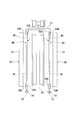
- FIG. 1 is a cross-sectional view schematically showing an example of a thin film solar cell 100 manufactured by the thin film solar cell manufacturing apparatus of the present invention.
- a thin film solar cell 100 includes a substrate W (for example, a glass substrate) constituting the surface thereof; an upper electrode 101 made of a transparent conductive film provided on the substrate W; and made of amorphous silicon.
- the thin film solar cell 100 is an amorphous silicon / microcrystal silicon tandem solar cell. In the thin film solar cell 100 having such a tandem structure, short wavelength light is absorbed by the top cell 102 and long wavelength light is absorbed by the bottom cell 104, thereby improving power generation efficiency.
- the top cell 102 has a three-layer structure of a p layer (102p), an i layer (102i), and an n layer (102n), and each is formed of amorphous silicon.
- the bottom cell 104 has a three-layer structure of a p-layer (104p), an i-layer (104i), and an n-layer (104n), and each is made of microcrystal silicon.
- the thin film solar cell 100 having such a configuration, when energetic particles called photons contained in sunlight hit the i layer, electrons and holes are generated by the photovoltaic effect, and the electrons go to the n layer. The holes move toward the p layer while moving toward the p layer. By extracting electrons / holes generated by the photovoltaic effect from the upper electrode 101 and the back electrode 106, light energy can be converted into electric energy.
- the intermediate electrode 103 By providing the intermediate electrode 103 between the top cell 102 and the bottom cell 104, a part of the light that passes through the top cell 102 and reaches the bottom cell 104 is reflected by the intermediate electrode 103 and incident on the top cell 102 side again. To do. Therefore, the sensitivity characteristic of the cell is improved, and the power generation efficiency can be improved.
- the sunlight incident from the substrate W side is reflected by the back electrode 106 after passing through each layer.
- a texture structure for the purpose of a prism effect for extending the optical path of sunlight incident on the upper electrode 101 and a light confinement effect is adopted in order to improve the conversion efficiency of light energy. ing.
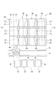
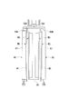
- FIG. 2 is a schematic plan view of a thin-film solar cell manufacturing apparatus according to an embodiment of the present invention.
- the thin-film solar cell manufacturing apparatus 10 includes a film formation chamber 11 in which a bottom cell 104 (semiconductor layer) made of microcrystalline silicon can be formed simultaneously on a plurality of substrates W;
- a loading / unloading chamber 13 capable of simultaneously accommodating a pre-deposition substrate W1 (substrate W) carried into the film chamber 11 and a post-deposition substrate W2 (substrate W) unloaded from the deposition chamber 11;
- a substrate removal chamber 15 for detaching the substrate W1 before film treatment and the substrate W2 after film formation from the carrier (transport section) 21 (see FIG.
- a substrate removal robot 17 for detaching the substrate W from the carrier 21; And a substrate storage cassette 19 for storing W for transporting it to another processing chamber.
- four substrate film forming lines 16 each including a film forming chamber 11, a preparation / removal chamber 13, and a substrate desorption chamber 15 are provided.
- the substrate removal robot 17 can move on a rail 18 laid on the floor surface. As a result, the transfer of the substrate W to all the substrate film forming lines 16 can be performed by a single substrate removal robot 17.
- the film forming chamber 11 and the loading / unloading chamber 13 are integrated to form a substrate film forming module 14, which has a size that can be loaded on a truck.
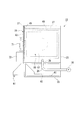
- FIGS. 3A to 3C are schematic configuration diagrams of the film forming chamber.
- 3A is a perspective view
- FIG. 3B is a perspective view when viewed from an angle different from FIG. 3A
- FIG. 3C is a side view.
- the film forming chamber 11 is formed in a box shape.
- Each of the carrier carry-in / out ports 24 is provided with a shutter 25 for opening and closing the carrier carry-in / out port 24.
- the carrier carry-in / out port 24 is sealed while ensuring airtightness.
- Three electrode units 31 for forming a film on the substrate W are attached to the second side surface 27 facing the first side surface 23. These electrode units 31 are detachable from the film forming chamber 11.
- a vacuum pump 30 for evacuating the space in the film forming chamber 11 is connected to the lower portion 28 of the third side surface of the film forming chamber 11 via an exhaust pipe 29 (see FIG. 3C. FIG. 3A and FIG. 3). (Not shown in 3B).
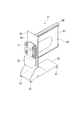
- FIG. 4A to 4D are schematic configuration diagrams of the electrode unit 31.
- FIG. 4A is a perspective view
- FIG. 4B is a perspective view when viewed from an angle different from FIG. 4A.
- FIG. 4C is a perspective view showing a modification of the electrode unit 31.
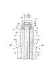
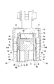
- FIG. 4D is a partial cross-sectional view of the cathode unit and the anode (counter electrode).
- the electrode unit 31 can be attached to and detached from three openings 26 formed on the second side surface 27 of the film forming chamber 11 (see FIG. 3B).
- the electrode unit 31 is provided with one wheel 61 at each of the four corners of the lower part (bottom plate part 62), and is movable on the floor surface.
- the bottom plate portion 62 with the wheels 61 may be a carriage 62A that can be separated from and connected to the side plate portion 63 to which the cathode unit 68, the anode unit 90, and the like are attached.
- the carriage 62A is separated from the side plate portion 63 to which the cathode unit 68, the anode unit 90, etc. are attached, and the other electrode unit 31 is used as a common carriage 62A. Can be used for moving.
- the side plate portion 63 of the electrode unit 31 forms part of the wall surface of the film forming chamber 11.
- An anode 67 and a cathode unit 68 disposed on both surfaces of the substrate W during the film forming process are provided on one surface 65 of the side plate portion 63 (a surface facing the inside of the film forming chamber 11).
- the electrode unit 31 of the present embodiment includes a pair of anodes 67 that are spaced apart on both sides of the cathode unit 68 therebetween. Then, two substrates W can be formed simultaneously with one electrode unit 31. Each substrate W at the time of film formation is disposed on both sides of the cathode unit 68 so as to face each other substantially parallel to the vertical direction.
- the two anodes 67 are arranged on the outer side in the thickness direction of each substrate W so as to face each substrate W.
- a driving mechanism (driving unit) 71 for driving the anode 67 and a matching box 72 for supplying power to the cathode unit 68 during film formation are attached to the other surface 69 of the side plate portion 63. Yes. Further, a connecting portion (not shown) for piping for supplying a film forming gas to the cathode unit 68 is formed on the side plate portion 63.
- the two (a pair) anodes 67 incorporate a heater H as a temperature control unit that controls the temperature of the substrate W. These two anodes 67 and the heater H constitute an anode unit 90.
- the two anodes 67 and 67 can be moved in a direction (horizontal direction) approaching and separating from each other by a drive mechanism 71 provided on the side plate portion 63, and the separation between the substrate W and the cathode unit 68. The distance can be controlled. Specifically, before the deposition of the substrate W, the two anodes 67 and 67 move toward the cathode unit 68 and come into contact with the substrate W.
- the two anodes 67 and 67 move in a direction approaching the cathode unit 68, and the separation distance between the substrate W and the cathode unit 68 is adjusted to a desired distance. Thereafter, film formation is performed, and after the film formation is completed, the anodes 67 and 67 are moved away from each other, the anode 67 and the substrate W are separated from each other, and the substrate W can be easily taken out from the electrode unit 31. Can do. Further, the anode 67 is attached to the drive mechanism 71 via a hinge (not shown).
- the surface 67A of the anode 67 facing the cathode unit 68 is opened and closed until it is substantially parallel to the one surface 65 of the side plate portion 63. I can move. That is, the anode 67 can be rotated by approximately 90 ° in plan view (see FIG. 4A).
- the cathode unit 68 includes a shower plate (cathode) 75, a cathode intermediate member 76, an exhaust duct 79, and a floating capacitance body 82.
- the cathode unit 68 is provided with a pair of shower plates 75 each having a plurality of small holes (not shown) formed on the surface facing each anode 67, and the film forming gas is directed toward the substrate W from the small holes. Erupted.
- the shower plates 75 and 75 form a cathode (high frequency electrode) electrically connected to the matching box 72.
- a cathode intermediate member 76 that is electrically connected to the matching box 72 is provided between the two shower plates 75 and 75. That is, the shower plate 75 is disposed on both side surfaces of the cathode intermediate member 76 in a state of being electrically connected to the cathode intermediate member 76.
- the cathode intermediate member 76 and the shower plate (cathode) 75 are formed of a conductor.
- the high frequency is applied to the shower plate (cathode) 75 through the cathode intermediate member 76. For this reason, the voltages applied to the two shower plates 75 and 75 for generating plasma have the same potential and the same phase.
- the cathode intermediate member 76 is electrically connected to the matching box 72 by a wiring (not shown).
- a space 77 is formed between the cathode intermediate member 76 and the shower plate 75.
- a film forming gas is introduced into the space 77 from a gas supply device (not shown).
- the pair of space portions 77 are separated by a cathode intermediate member 76 interposed therebetween, and are formed separately corresponding to each shower plate 75, 75. Therefore, the flow rate and type of gas discharged from each shower plate 75, 75 can be controlled independently. That is, the space 77 has a role of a gas supply path.
- each of the space portions 77 is formed separately corresponding to each of the shower plates 75 and 75, so the cathode unit 68 has two gas supply paths. .
- a hollow exhaust duct 79 is provided around the entire periphery of the cathode unit 68.
- the exhaust duct 79 is formed with an exhaust port 80 through which the film forming gas and reaction by-product (powder) in the film forming space 81 are introduced into the exhaust duct 79 and exhausted.
- an exhaust port 80 is formed facing a film formation space 81 formed between the substrate W and the shower plate 75 when film formation is performed.
- a plurality of the exhaust ports 80 are formed along the peripheral edge of the cathode unit 68, and are configured to be able to exhaust substantially uniformly over the entire periphery.
- An opening ⁇ (not shown) is formed in a surface facing the film forming chamber 11 in the exhaust duct 79 disposed in the lower part of the cathode unit 68.
- the film forming gas exhausted from the film forming space 81 is discharged into the film forming chamber 11 through the opening ⁇ .
- the gas discharged into the film forming chamber 11 is exhausted to the outside through an exhaust pipe 29 provided in the lower side surface 28 of the film forming chamber 11 (see FIG. 3C).
- a stray capacitance body 82 having a dielectric and / or a laminated space of the dielectric is provided.
- the exhaust duct 79 is connected to the ground potential.
- the exhaust duct 79 also functions as a shield frame for preventing abnormal discharge from the cathode 75 and the cathode intermediate member 76.
- a pair of masks 78 are provided on the peripheral edge of the cathode unit 68 so as to cover a portion from the outer periphery of the exhaust duct 79 to the outer periphery of the shower plate (cathode) 75.
- These masks 78 cover sandwiching pieces 59A (see FIGS. 9 and 21) of the sandwiching portion 59, which will be described later, provided on the carrier 21, and the deposition gas and reaction by-products (powder) in the deposition space 81. Is formed in the gas flow path R. That is, the gas flow path R is formed between the mask 78 and the shower plate 75 and between the mask 78 and the stray capacitance body 82.
- a plurality of moving rails 37 are provided between the film forming chambers 11 and 11 so that the carrier 21 can move between the film forming chamber 11 and the loading / unloading chamber 13 and between the loading / unloading chamber 13 and the substrate removal chamber 15. It is laid between the substrate removal chambers 15 (see FIG. 2).
- the moving rail 37 is separated between the film forming chamber 11 and the loading / unloading chamber 13, and the carrier carry-in / out port 24 is sealed by closing the shutter 25.
- FIGS. 5A and 5B are schematic perspective views of the preparation / removal chamber 13.
- 5A is a perspective view
- FIG. 5B is a perspective view when viewed from an angle different from FIG. 5A.
- the preparation / removal chamber 13 is formed in a box shape.
- the first side surface 33 is connected to the first side surface 23 of the film forming chamber 11 while ensuring airtightness.
- the first side surface 33 is formed with an opening 32 through which the three carriers 21 can be inserted.
- the second side surface 34 facing the first side surface 33 is connected to the substrate desorption chamber 15.
- the second side surface 34 is formed with three carrier carry-in / out ports 35 through which the carrier 21 on which the substrate W is mounted can pass.
- the carrier carry-in / out port 35 is provided with a shutter 36 that can ensure airtightness.
- Each moving rail 37 is separated between the preparation / removal chamber 13 and the substrate removal chamber 15, and the carrier carry-in / out port 35 is sealed by closing the shutter 36.
- the preparation / removal chamber 13 is provided with a push-pull mechanism 38 for moving the carrier 21 between the film formation chamber 11 and the preparation / removal chamber 13 along the moving rail 37.
- the push-pull mechanism 38 includes a locking portion 48 for locking the carrier 21; a pair of guides provided at both ends of the locking portion 48 and arranged substantially parallel to the moving rail 37. A member 49; and a moving device 50 for moving the locking portion 48 along both guide members 49.
- a movement mechanism (not shown) is provided in the preparation / removal chamber 13 for simultaneously accommodating the pre-deposition substrate W1 and the post-deposition substrate W2.
- This moving mechanism moves the carrier 21 by a predetermined distance in a direction substantially orthogonal to the laying direction of the moving rail 37 in plan view.
- a vacuum pump 43 for evacuating the inside of the preparation / removal chamber 13 is connected to the lower portion 41 of the third side surface of the preparation / removal chamber 13 via an exhaust pipe 42 (see FIG. 5B).
- FIGS. 7A and 7B are schematic configuration diagrams of the substrate desorption chamber.
- 7A is a perspective view
- FIG. 7B is a front view.
- the substrate desorption chamber 15 is formed of a frame-like body and connected to the second side surface 34 of the preparation / removal chamber 13.
- the attachment of the substrate W1 before the film formation process and the removal of the substrate W2 after the film formation process are performed on the carrier 21 arranged on the moving rail 37.
- three carriers 21 can be arranged in parallel.
- the substrate removal robot 17 has a drive arm 45.
- the drive arm 45 can suck the substrate W at its tip. Further, the drive arm 45 can move between the carrier 21 disposed in the substrate removal chamber 15 and the substrate storage cassette 19. The drive arm 45 takes out the pre-deposition substrate W1 from the substrate storage cassette 19, and The substrate W1 before film formation can be attached to the carrier 21 disposed in the substrate desorption chamber 15. Further, the drive arm 45 can also remove the post-deposition substrate W ⁇ b> 2 from the carrier 21 that has returned to the substrate removal chamber 15 and transport it to the substrate storage cassette 19.
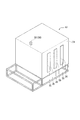
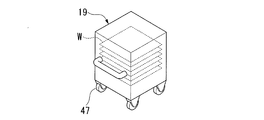
- FIG. 8 is a perspective view of the substrate storage cassette 19.
- the substrate storage cassette 19 is formed in a box shape and has a size capable of storing a plurality of substrates W.
- a plurality of substrates W can be stacked and stored in the vertical direction with the film formation surface horizontal.
- casters 47 are provided at the four corners below the substrate storage cassette 19 so that they can be easily moved to another processing apparatus.
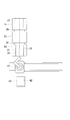
- FIG. 9 is a perspective view of a carrier for transporting the substrate W.
- the carrier 21 includes two frame-shaped frames 51 to which the substrate W can be attached. That is, two substrates W can be attached to one carrier 21.
- the two frames 51 and 51 are connected by a connecting member 52 at the upper part thereof.
- a plurality of wheels 53 placed on the moving rail 37 are provided on the upper surface of the connecting member 52. These wheels 53 roll on the moving rail 37 so that the carrier 21 can move along the moving rail 37.
- a frame holder 54 is provided below the frame 51 for suppressing the shaking of the substrate W when the carrier 21 moves.
- the lower end of the frame holder 54 is fitted to a rail member 55 having a concave cross section provided on the bottom surface of each chamber.
- the rail member 55 is arranged along the moving rail 37 when viewed in plan. If the frame holder 54 is composed of a plurality of rollers, more stable conveyance is possible.
- Each frame 51 has a peripheral portion 57 and a sandwiching portion 59.
- the film formation surface of the substrate W is exposed to the opening 56 formed in the frame 51.
- the clamping part 59 clamps and fixes the board
- An urging force is applied to the holding portion 59 holding the substrate W by a spring or the like.
- the sandwiching portion 59 has sandwiching pieces 59 ⁇ / b> A and 59 ⁇ / b> B that abut on the front surface WO (film formation surface) and the back surface WU (back surface) of the substrate W, respectively.
- the distance between the sandwiching piece 59A and the sandwiching piece 59B can be varied via the spring or the like. That is, the separation distance can be varied along the direction in which the sandwiching piece 59A approaches and separates from the sandwiching piece 59B according to the movement of the anode 67 (details will be described later).
- one carrier 21 one carrier 21 capable of holding a pair (two) of substrates W
- the thin-film solar cell manufacturing apparatus 10 of this embodiment four sets of the substrate film forming lines 16 described above are arranged, and three carriers 21 are accommodated in one film forming chamber 11, so that 24 substrates W are omitted. A film can be formed simultaneously.
- the drive arm 45 of the substrate removal robot 17 is moved to take out one pre-deposition substrate W ⁇ b> 1 from the substrate storage cassette 19 and attach it to the carrier 21 in the substrate removal chamber 15.
- the orientation of the pre-deposition substrate W1 disposed in the horizontal direction on the substrate accommodating cassette 19 is changed to the vertical direction and attached to the carrier 21.
- This operation is repeated once, and two substrates W1 before film formation are attached to one carrier 21.
- this operation is repeated to attach the pre-deposition substrate W1 to the remaining two carriers 21 in the substrate removal chamber 15 respectively. That is, six substrates W1 before film formation are attached at this stage.
- the three carriers 21 to which the pre-deposition substrate W 1 is attached are moved substantially simultaneously along the respective moving rails 37 and accommodated in the preparation / removal chamber 13.
- the shutter 36 of the carrier carry-in / out port 35 of the preparation / removal chamber 13 is closed.
- the inside of the preparation / removal chamber 13 is kept in a vacuum state using the vacuum pump 43.
- the three carriers 21 are respectively moved by a predetermined distance in the direction orthogonal to the direction in which each moving rail 37 is laid in a plan view.
- the shutter 25 of the film forming chamber 11 is opened, and the carrier 21 ⁇ / b> A to which the post-deposition substrate W ⁇ b> 2 that has been formed in the film forming chamber 11 is attached is loaded and taken out. 13 is moved using a push-pull mechanism 38.
- the carrier 21 holding the pre-film formation substrate W1 and the carrier 21A holding the post-film formation substrate W2 are alternately arranged in parallel. Then, by maintaining this state for a predetermined time, the heat stored in the substrate W2 after the film formation process is transferred to the substrate W1 before the film formation process. That is, the substrate W1 before film formation is heated.
- the movement of the push-pull mechanism 38 will be described.
- the movement when the carrier 21A in the film forming chamber 11 is moved into the preparation / removal chamber 13 will be described.
- the carrier 21A to which the post-deposition substrate W2 is attached is locked to the locking portion 48 of the push-pull mechanism 38.
- the moving arm 58 of the moving device 50 attached to the locking portion 48 is swung.
- the length of the moving arm 58 is variable.
- the locking portion 48 that locks the carrier 21A moves while being guided by the guide member 49, and the carrier 21A moves from the film formation chamber 11 into the preparation / removal chamber 13 as shown in FIG. 15B.
- the carrier 21 and the carrier 21 ⁇ / b> A are moved in a direction orthogonal to the moving rail 37 by the moving mechanism, and the carrier 21 holding the substrate W ⁇ b> 1 before film formation is moved to each moving rail 37. Move to position.
- each carrier 21 holding the pre-deposition substrate W1 is moved into the film formation chamber 11 using the push-pull mechanism 38, and the shutter 25 is closed after the movement is completed.
- a vacuum state is maintained in the film forming chamber 11.
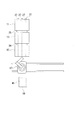
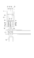
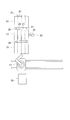
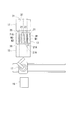
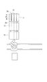
- the pre-deposition substrate W1 attached to each carrier 21 moves along the surface direction thereof, and the pre-deposition process is performed between the anode 67 and the cathode unit 68 in the deposition chamber 11. It is inserted so that the surface WO of the substrate W1 is substantially parallel to the vertical direction (see FIG. 18).
- the two anodes 67 are moved toward each other by the drive mechanism 71 so that the anodes 67 are brought into contact with the back surface WU of the substrate W1 before film formation. Make contact.
- the pre-deposition substrate W1 moves toward the cathode unit 68 so as to be pushed by the anode 67. Further, the pre-deposition substrate W1 is moved until the gap between the pre-deposition substrate W1 and the shower plate 75 of the cathode unit 68 reaches a predetermined distance (deposition distance).
- the gap (deposition distance) between the pre-deposition substrate W1 and the shower plate 75 of the cathode unit 68 is in the range of 5 to 15 mm, and is preferably about 5 mm, for example.
- the holding piece 59A of the holding portion 59 of the carrier 21 that is in contact with the surface WO side of the substrate W1 before the film formation process moves along with the movement of the substrate W1 before the film formation process (movement of the anode 67). Displacement in a direction away from 59B.
- the substrate W1 before film formation is sandwiched between the anode 67 and the sandwiching piece 59A.
- a restoring force such as a spring (not shown) acts on the sandwiching piece 59A, so that the sandwiching piece 59A is displaced toward the sandwiching piece 59B.
- the sandwiching piece 59A comes into contact with the mask 78, and the movement of the anode 67 stops at this point (see FIG. 21).
- the mask 78 covers the surface of the sandwiching piece 59 ⁇ / b> A and the outer edge portion of the substrate W, and is in close contact with the sandwiching piece 59 ⁇ / b> A or the outer edge portion of the substrate W. That is, the mating surface between the mask 78 and the sandwiching piece 59A or the outer edge portion of the substrate W has a role of a sealing surface.
- the film forming gas hardly leaks to the anode 67 side from between the mask 78 and the sandwiching piece 59A or the outer edge portion of the substrate W.
- the range in which the film forming gas spreads is limited, and formation of a film on the unnecessary range, that is, the outer edge of the anode 67 or the substrate W can be prevented.
- the mask 78 can be separated from the film forming chamber 11 integrally with the electrode unit 31, the mask 89 can be easily cleaned. As a result, the operating rate of the thin-film solar cell manufacturing apparatus 10 is improved.
- the gap between the mask 78 and the shower plate 75 and the gap between the mask 78 and the exhaust duct 79, that is, the channel dimension in the thickness direction of the gas channel R are determined as follows. Is set to be a predetermined distance. As another form, the distance between the substrate W and the shower plate (cathode) 75 can be arbitrarily changed by the stroke of the drive mechanism 71 by attaching the mask 78 to the exhaust duct 79 via an elastic body. In the above-described embodiment, the mask 78 and the substrate W are in contact with each other. However, the mask 78 and the substrate W may be arranged so as to leave a minute space that restricts the passage of the film forming gas. .
- the film forming gas is ejected from the shower plate 75 of the cathode unit 68 and the matching box 72 is activated to apply a voltage to the cathode 76 of the cathode unit 68.
- plasma is generated in the film formation space 81 and film formation is performed on the surface WO of the substrate W1 before film formation.
- the substrate W1 before film formation is heated to a desired temperature by a heater H (for example, a heating wire) built in the anode 67.
- the anode 67 stops heating when the pre-deposition substrate W1 reaches a desired temperature.
- a voltage is applied to the shower plate (cathode) 75 and plasma is generated in the film formation space 81, the film formation process is performed even if heating of the anode 67 is stopped due to heat input from the plasma over time.
- the temperature of the front substrate W1 may rise higher than a desired temperature.
- the anode 67 can also function as a heat sink for cooling the pre-deposition substrate W1 whose temperature has increased excessively. Therefore, the substrate W1 before the film formation process is adjusted to a desired temperature regardless of the elapsed time of the film formation process time.
- the film forming gas material to be supplied can be switched every predetermined time.
- gas and reaction by-products (powder) in the film formation space 81 pass through the gas flow path R to the exhaust duct 79 from the exhaust port 80 formed at the peripheral edge of the cathode unit 68. And flows in.
- the gas that has flowed into the exhaust duct 79 passes through the opening ⁇ of the exhaust duct 79 disposed at the lower portion of the cathode unit 68, and goes to the outside from the exhaust pipe 29 provided at the lower side surface 28 of the film forming chamber 11. And exhausted.
- reaction by-products (powder) generated during film formation can be collected and disposed by adhering and depositing on the inner wall surface of the exhaust duct 79. Since all the electrode units 31 in the film forming chamber 11 perform the same process as described above, the film forming process can be simultaneously performed on all the six substrates.
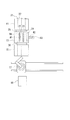
- the two anodes 67 are moved away from each other by the drive mechanism 71, and the substrate W2 and the frame 51 (the sandwiching piece 59A) after the film forming process are returned to their original positions (FIG. 19). reference). That is, when the film formation is completed and the carrier 21 is moved, the mask 78 is detached from the exposed surface 85 of the sandwiching piece 59A. Further, by moving the anode 67 in a direction away from each other, the substrate W2 after the film formation process and the anode 67 are separated from each other (see FIG. 18).
- the shutter 25 of the film formation chamber 11 is opened, and each carrier 21 is moved into the preparation / removal chamber 13 using a push-pull mechanism 38.
- the inside of the preparation / removal chamber 13 is evacuated, and the carrier 21B attached with the pre-deposition substrate W1 to be formed next is already arranged.
- the heat storage of the substrate W2 after the film formation process is transferred to the substrate W1 before the film formation process in the preparation / removal chamber 13, and the temperature of the substrate W2 after the film formation process is lowered.
- each carrier 21B is moved into the film forming chamber 11
- each carrier 21 is returned to the position of the moving rail 37 by the moving mechanism.
- the substrate W2 after each film formation process is removed from each carrier 21 by the substrate removal robot 17 and moved to the substrate accommodation cassette 19 in the substrate removal chamber 15.
- the film forming process is completed by moving the substrate storage cassette 19 to the place of the next process.
- the anode 67 moves along the direction approaching / separating from the cathode (shower plate 75). Therefore, when the substrate W is taken in and out of the film forming chamber 11, the anode 67 is moved.
- the gap between 67 and the cathode (shower plate 75) can be set large.
- the gap between the pre-deposition substrate W1 and the shower plate 75 of the cathode unit 68 is reduced to a predetermined distance (film formation distance).
- this predetermined distance can be set to about 5 mm.
- the cathode unit 68 that is relatively difficult to move is disposed between the two substrates W, that is, approximately in the center of the film forming chamber 11.
- the anode 67 that is relatively easy to move is arranged outside the two substrates W, that is, on the side surface inside the film forming chamber 11. Then, the anode 67 can be moved by the drive mechanism 71 to control the separation distance between the substrate W and the cathode unit 68. For this reason, compared with the case where the cathode unit 68 is moved, complication of the thin film solar cell manufacturing apparatus 10 can be suppressed, and the manufacturing cost of the thin film solar cell manufacturing apparatus 10 can be reduced.
- the two anodes 67 of the electrode unit 31 are moved toward each other by the drive mechanism 71, and the anode 67 and the back surface WU of the substrate W1 before film formation processing are brought into contact with each other. .
- the pre-deposition substrate W1 is moved toward the cathode unit 68 so that the driving mechanism 71 is driven and pushed by the anode 67.
- the anode 67 incorporates a heater H, and the anode 67 and the heater H constitute an anode unit 90. For this reason, since no film is interposed between the anode 67 and the substrate W when the film is formed, the substrate W can be efficiently heated.
- the anode 67 can be used as a heat dissipation medium for the substrate W. Therefore, it becomes possible to keep the substrate W constant at a desired temperature regardless of the elapsed time of the film formation processing time, and a higher quality film can be formed.
- a hollow exhaust duct 79 is provided on the peripheral edge of the cathode unit 68 over substantially the entire circumference.
- the film forming gas exhaust gas
- exhaust efficiency can be improved.
- reaction by-products (powder) generated during film formation can be easily recovered.
- This reaction by-product (powder) can be collected and disposed by adhering to the inner wall surface of the exhaust duct 79. For this reason, it is possible to make the film forming gas exhausted to the outside from the exhaust pipe 29 provided in the lower side surface 28 of the film forming chamber 11 into a relatively clean state containing no reaction by-products (powder). become.
- the clamping part 59 provided in the carrier 21 has clamping pieces 59A and 59B that come into contact with the front surface WO and the rear surface WU of the substrate W.
- the separation distance of the sandwiching pieces 59A and 59B can be changed via a spring or the like, that is, the sandwiching piece 59A can move along the direction in which the sandwiching piece 59A approaches or approaches the sandwiching piece 59B in accordance with the movement of the anode 67. It is configured. For this reason, the substrate W can be easily moved close to and away from the cathode unit 68 as the anode 67 moves.
- the shower plates 75 and 75 are cathodes (high frequency electrodes) connected to the matching box 72, it is not necessary to provide the cathode and the shower plate 75 separately. As a result, the thin-film solar cell manufacturing apparatus 10 can be simplified and reduced in cost.
- the cathode unit 68 includes a shower plate (cathode) 75, a cathode intermediate member 76, an exhaust duct 79, and a stray capacitance body 82.
- the pair of shower plates 75 are disposed on both side surfaces of the cathode intermediate member 76 in a state of being electrically connected to the cathode intermediate member 76.
- the cathode intermediate member 76 and the shower plate (cathode) 75 are formed of a conductor, and the high frequency is applied to each shower plate (cathode) 75 via the cathode intermediate member 76. Therefore, a voltage having the same potential and the same phase for generating plasma is applied to the pair of shower plates 75 and 75.
- the space 77 (gas supply path) is separated by the cathode intermediate member 76 and formed separately corresponding to each shower plate 75, 75. Therefore, the gas emitted from each shower plate 75, 75 can be controlled independently. For this reason, according to the use condition of the thin film solar cell manufacturing apparatus 10, the film-forming gas discharge
Landscapes
- Chemical & Material Sciences (AREA)
- Engineering & Computer Science (AREA)
- Materials Engineering (AREA)
- General Chemical & Material Sciences (AREA)
- Chemical Kinetics & Catalysis (AREA)
- Mechanical Engineering (AREA)
- Metallurgy (AREA)
- Organic Chemistry (AREA)
- Plasma & Fusion (AREA)
- Physics & Mathematics (AREA)
- Inorganic Chemistry (AREA)
- Photovoltaic Devices (AREA)
- Chemical Vapour Deposition (AREA)
Abstract
Description
本願は、2008年6月6日に、日本に出願された特願2008-149934号に基づき優先権を主張し、その内容をここに援用する。
この薄膜太陽電池の薄膜Si層(半導体層)の成膜には、プラズマCVD装置を用いることが多い。この種のプラズマCVD装置としては、枚葉式PE-CVD(プラズマCVD)装置、インライン型PE-CVD装置、バッチ式PE-CVD装置などが存在する。
しかしながら、上述の従来技術では、キャリアに垂設された支持壁に基板を支持させ、この状態で成膜室に基板を搬送するので、キャリアのガタなどを考慮すると、基板と高周波電極との隙間を5mm程度に設定するのが困難である。この隙間が大きくなると、薄膜Si層の品質が低下してしまうおそれがある。
また、キャリアによって成膜室に搬送されてきた基板と高周波電極との隙間を5mm程度に設定できたとしても、この隙間が装置の大きさを考えると微小であるため、成膜室からの基板の出し入れ作業が行い難い。このため、従来では、アノードとなるバックプレートを基板と一体として搬送する場合もあったが、搬送対象が大型化することにより、搬送機構が大型化していた。
(1)本発明の薄膜太陽電池製造装置は、基板の成膜面と重力方向とが略並行となるように前記基板が配置され、前記成膜面にCVD法により膜を形成する成膜室と;電圧が印加されるカソードが両側に配置されたカソードユニットと、前記各カソードのそれぞれに対向かつ離間距離を置いて配置された一対のアノードと、を有する電極ユニットと;前記基板を支持し、前記カソードとこれに対向する前記アノードとの間に前記基板を搬送する搬送部と;を有し、前記離間距離が可変である。
また、基板を出し入れする際に基板がアノードやカソードユニットに接触して損傷するのを防止できる。
また、排気ダクトを用いて排気させることで、例えば、基板の成膜面に膜を形成する際に発生した反応副生成物(パウダー)なども、容易に回収できる。この場合、排気ダクトの内壁に反応副生成物(パウダー)を付着・堆積させることで、反応副生成物(パウダー)を含まない比較的クリーンな成膜ガスを排気させることが可能になる。
(薄膜太陽電池)
図1は、本発明の薄膜太陽電池製造装置で製造される薄膜太陽電池100の一例を、模式的に示した断面図である。図1に示すように、薄膜太陽電池100は、その表面を構成する基板W(例えばガラス基板など)と;この基板W上に設けられた透明導電膜からなる上部電極101と;アモルファスシリコンからなるトップセル102と;このトップセル102と後述するボトムセル104との間に設けられた透明導電膜からなる中間電極103と;マイクロクリスタルシリコンからなるボトムセル104と;透明導電膜からなるバッファ層105と;金属膜からなる裏面電極106と;が積層して構成されている。つまり、薄膜太陽電池100は、アモルファスシリコン/マイクロクリスタルシリコンタンデム型太陽電池である。このようなタンデム構造の薄膜太陽電池100では、短波長光をトップセル102で吸収するとともに、長波長光をボトムセル104で吸収することで、発電効率の向上を図ることができる。
図2は、本発明の一実施形態に係る薄膜太陽電池製造装置の概略平面図である。図2に示すように、この薄膜太陽電池製造装置10は、複数の基板Wに対してマイクロクリスタルシリコンで構成されたボトムセル104(半導体層)を同時に成膜可能な成膜室11と;この成膜室11に搬入される成膜処理前基板W1(基板W)、及び成膜室11から搬出された成膜処理後基板W2(基板W)を同時に収容可能な仕込・取出室13と;成膜処理前基板W1および成膜処理後基板W2をキャリア(搬送部)21(図9参照)に脱着する基板脱着室15と;基板Wをキャリア21から脱着するための基板脱着ロボット17と;基板Wを別の処理室に搬送するために収容する基板収容カセット19と;を備えている。本実施形態では、成膜室11、仕込・取出室13および基板脱着室15で構成される基板成膜ライン16が、4つ設けられている。基板脱着ロボット17は、床面に敷設されたレール18上を移動できるようになっている。これにより、全ての基板成膜ライン16への基板Wの受け渡しを、1台の基板脱着ロボット17で行えるようになっている。さらに、成膜室11と仕込・取出室13とが一体化して基板成膜モジュール14を構成しており、トラックに積載可能な大きさを有している。
これら図3A~図3Cに示すように、成膜室11は、箱型に形成されている。成膜室11の、仕込・取出室13と接続される第一側面23には、基板Wが搭載されたキャリア21が通過可能なキャリア搬出入口24が、3箇所形成されている。これらキャリア搬出入口24には、これらキャリア搬出入口24を開閉するシャッタ25がそれぞれ設けられている。シャッタ25を閉じた場合、キャリア搬出入口24は気密性を確保して封止される。第一側面23と対向する第二側面27には、基板Wに成膜を施すための電極ユニット31が3基取り付けられている。これら電極ユニット31は、成膜室11から着脱可能である。成膜室11の第三側面下部28には、成膜室11内の空間を真空排気するための真空ポンプ30が、排気管29を介して接続されている(図3C参照。図3A及び図3Bでは図示略)。
電極ユニット31は、成膜室11の第二側面27に形成された3箇所の開口部26に着脱可能である(図3B参照)。電極ユニット31は、下部(底板部62)の四隅に車輪61が1つずつ設けられており、床面上を移動可能である。車輪61が取り付けられた底板部62上には、側板部63が鉛直方向に沿って立設されている。この側板部63は、成膜室11の第二側面27の開口部26を閉塞できる大きさを有している。
図4Cの変形例に示すように、車輪61付きの底板部62は、カソードユニット68やアノードユニット90等が取り付けられた側板部63と分離・接続可能な台車62Aとしてもよい。この場合、電極ユニット31を成膜室11に接続した後に、カソードユニット68やアノードユニット90等が取り付けられた側板部63から台車62Aを分離し、共通の台車62Aとして、他の電極ユニット31の移動に使用できる。
さらに、アノード67は、駆動機構71にヒンジ(不図示)を介して取りつけられている。これにより、電極ユニット31を成膜室11から引き抜いた状態で、アノード67のカソードユニット68側を向いた面67Aが、側板部63の一方の面65と略平行になるまで開閉するように回動できる。つまり、アノード67は平面視において略90°回動できるようになっている(図4A参照)。
カソードユニット68には、各アノード67と対向する面にそれぞれ小孔(不図示)が複数形成された一対のシャワープレート75が配置されており、この小孔から成膜ガスが基板Wに向かって噴出される。このシャワープレート75,75は、前記マッチングボックス72と電気的に接続されたカソード(高周波電極)をなしている。2枚のシャワープレート75,75の間には、マッチングボックス72と電気的に接続されたカソード中間部材76が設けられている。すなわち、シャワープレート75は、カソード中間部材76の両側面に、このカソード中間部材76と電気的に接続された状態で配置されている。
カソード中間部材76は、図示しない配線によって前記マッチングボックス72と電気的に接続されている。カソード中間部材76とシャワープレート75との間には、空間部77が形成されている。そして、ガス供給装置(不図示)より、この空間部77に成膜ガスが導入されるようになっている。一対の空間部77は、これらの間に介在するカソード中間部材76で分離され、それぞれのシャワープレート75、75毎に対応して別々に形成されている。そのため、各シャワープレート75、75から放出されるガスの流量や種類を独立して制御できる。すなわち、空間部77は、ガス供給路の役割を有している。本実施形態にあっては、各空間部77のそれぞれが、シャワープレート75、75毎に対応して別々に形成されているので、カソードユニット68は、2系統のガス供給路を有している。
カソードユニット68の下部に配された排気ダクト79には、成膜室11へ向いた面に開口部α(不図示)が形成されている。この開口部αによって、成膜空間81から排気された成膜ガスなどが、成膜室11内へ排出される。成膜室11内へ排出されたガスは、成膜室11の側面下部28に設けられた排気管29より外部へ排気される(図3C参照)。
排気ダクト79とカソード中間部材76の間には、誘電体および/もしくはこの誘電体の積層空間を有する浮遊容量体82が設けられている。
排気ダクト79は、接地電位に接続されている。排気ダクト79は、カソード75およびカソード中間部材76からの異常放電を防止するためのシールド枠としても機能する。
仕込・取出室13の第三側面下部41には、仕込・取出室13内を真空排気するための真空ポンプ43が、排気管42を介して接続されている(図5B参照)。
次に、本実施形態の薄膜太陽電池製造装置10を用いて、基板Wに成膜する方法を説明する。この説明においては、一組の基板成膜ライン16の図面を用いるが、他の三組の基板成膜ライン16も略同一の流れで基板Wを成膜する。
まず、図10に示すように、成膜処理前基板W1を複数枚収容した基板収容カセット19を所定の位置に配置する。
さらにこの動作を繰り返して、基板脱着室15内の残り二つのキャリア21にも、成膜処理前基板W1をそれぞれ取り付ける。つまり、この段階で成膜処理前基板W1を6枚取り付ける。
図15Aに示すように、プッシュ-プル機構38の係止部48に対し、成膜処理後基板W2が取り付けられたキャリア21Aを係止させる。そして、係止部48に取り付けられている移動装置50の移動アーム58を揺動させる。この時、移動アーム58の長さは可変する。すると、キャリア21Aを係止した係止部48が、ガイド部材49に案内されながら移動し、図15Bに示すように、キャリア21Aが成膜室11から仕込・取出室13内へと移動する。このように構成することで、キャリア21Aを駆動させるための駆動源を成膜室11内に設けることが不要になる。
図21に示すように、マスク78は、挟持片59Aの表面と基板Wの外縁部を覆うと共に、挟持片59Aもしくは基板Wの外縁部と密接するよう形成されている。すなわち、マスク78と、挟持片59Aもしくは基板Wの外縁部との合わせ面は、シール面の役割を有している。そのため、これらマスク78と、挟持片59Aもしくは基板Wの外縁部との間から、成膜ガスがアノード67側にほとんど漏れないようになっている。これにより、成膜ガスが広がる範囲が制限され、不要な範囲、つまり、アノード67や基板Wの外縁部への膜の形成を防止できる。さらに、マスク78が電極ユニット31と一体で成膜室11から分離できるので、マスク89のクリーニングが容易になる。この結果、薄膜太陽電池製造装置10の稼働率が向上する。
別の形態として、マスク78を排気ダクト79に対して弾性体を介して取り付けることによって、基板Wとシャワープレート(カソード)75の距離を、駆動機構71のストロークによって任意に変更することもできる。上記の実施形態では、マスク78と基板Wとが当接するものとしたが、成膜ガスの通過を制限するような微少な間隔を空けるように、マスク78と基板Wとを配置させても良い。
一度の成膜処理工程で複数の層を成膜する際には、供給する成膜ガス材料を所定時間毎に切り替えることで実施できる。
成膜室11内の全ての電極ユニット31において、上述した処理と同じ処理を実行するので、6枚の基板全てに対して同時に成膜処理を施すことができる。
さらにアノード67を互いに離間する方向に移動させることで、成膜処理後基板W2とアノード67とが離間する(図18参照)。
また、排気ダクト79を用いて排気させることで、例えば、成膜を施す際に発生した反応副生成物(パウダー)なども容易に回収できる。この反応副生成物(パウダー)は、排気ダクト79の内壁面に付着させることで回収・処分できる。このため、成膜室11の側面下部28に設けられた排気管29から外部へと排気される成膜ガスを、反応副生成物(パウダー)を含まない比較的クリーンな状態にすることが可能になる。
このため、一対のシャワープレート(カソード)75,75をそれぞれ別個に制御することなく、容易に同電位・同位相の電圧を印加することが可能になる。このため、電圧制御装置などの構成を簡略化することができ、薄膜太陽電池製造装置10の低コスト化を図ることができる。
11 成膜室
21 キャリア(搬送部)
59 挟持部
59A 挟持片(第一挟持片)
59B 挟持片(第二挟持片)
67 アノード
68 カソードユニット
71 駆動機構(駆動部)
75 シャワープレート兼カソード
76 カソード中間部材
77 空間部(ガス供給路)
79 排気ダクト
80 排気口
81 成膜空間
82 浮遊容量体
H ヒータ(温度制御部)
R ガス流路
W 基板
W1 成膜処理前基板
W2 成膜処理後基板
WO 表面(成膜面)
WU 裏面(背面)
Claims (9)
- 基板の成膜面と重力方向とが略並行となるように前記基板が配置され、前記成膜面にCVD法により膜を形成する成膜室と;
電圧が印加されるカソードが両側に配置されたカソードユニットと、前記各カソードのそれぞれに対向かつ離間距離を置いて配置された一対のアノードと、を有する電極ユニットと;
前記基板を支持し、前記カソードとこれに対向する前記アノードとの間に前記基板を搬送する搬送部と;
を有し、
前記離間距離が可変である
ことを特徴とする薄膜太陽電池製造装置。 - 前記電極ユニットが、前記アノードを前記カソードに対して接近・離間する方向に移動させる駆動部をさらに有することを特徴とする請求項1に記載の薄膜太陽電池製造装置。
- 前記アノードが前記カソードに対して接近する間に、前記基板に前記アノードが当接しながら移動することによって、前記基板の成膜面と前記カソードとの離間距離が制御されることを特徴とする請求項2に記載の薄膜太陽電池製造装置。
- 前記カソードが、前記基板の前記成膜面に対して成膜ガスを供給するシャワープレートであることを特徴とする請求項1乃至3の何れか1項に記載の薄膜太陽電池製造装置。
- 前記カソードユニットが、導電体からなるカソード中間部材をさらに有し;
一対の前記カソードが前記カソード中間部材に接続されている;
ことを特徴とする請求項4に記載の薄膜太陽電池製造装置。 - 前記カソードユニットが、2系統のガス供給路をさらに有し;
これらガス供給路のそれぞれが、対応する前記各カソードに接続され、前記各カソードの一方から放出される成膜ガスの流量や種類が他方とは独立して制御される;
ことを特徴とする請求項4に記載の薄膜太陽電池製造装置。 - 前記カソードユニットの外周面に、前記成膜ガスを排気する排気ダクトが配されていることを特徴とする請求項4に記載の薄膜太陽電池製造装置。
- 前記搬送部が、前記基板の前記成膜面に当接する第一挟持片と、前記基板の背面に当接する第二挟持片とを有し;
これら第一挟持片と第二挟持片とで前記基板が挟持され;
前記アノードが前記カソードユニットに対して接近する際に、前記第一挟持片が前記第二挟持片から離間し;
前記アノードが前記カソードユニットに対して離間する際に、前記第一挟持片が前記第二挟持片に接近する
ことを特徴とする請求項1乃至7の何れか1項に記載の薄膜太陽電池製造装置。 - 前記アノードに、前記基板の温度を制御するための温度制御部が内蔵されていることを特徴とする請求項1乃至8の何れかに記載の薄膜太陽電池製造装置。
Priority Applications (5)
| Application Number | Priority Date | Filing Date | Title |
|---|---|---|---|
| JP2010515909A JP5427779B2 (ja) | 2008-06-06 | 2009-06-04 | 薄膜太陽電池製造装置 |
| KR1020107023584A KR101195088B1 (ko) | 2008-06-06 | 2009-06-04 | 박막 태양 전지 제조 장치 |
| EP09758384.3A EP2290700B1 (en) | 2008-06-06 | 2009-06-04 | Apparatus for manufacturing thin film solar cell |
| CN2009801124278A CN101999172B (zh) | 2008-06-06 | 2009-06-04 | 薄膜太阳能电池制造装置 |
| US12/995,304 US20110107969A1 (en) | 2008-06-06 | 2009-06-04 | Apparatus for manufacturing thin-film solar cell |
Applications Claiming Priority (2)
| Application Number | Priority Date | Filing Date | Title |
|---|---|---|---|
| JP2008149934 | 2008-06-06 | ||
| JP2008-149934 | 2008-06-06 |
Publications (1)
| Publication Number | Publication Date |
|---|---|
| WO2009148117A1 true WO2009148117A1 (ja) | 2009-12-10 |
Family
ID=41398190
Family Applications (1)
| Application Number | Title | Priority Date | Filing Date |
|---|---|---|---|
| PCT/JP2009/060247 Ceased WO2009148117A1 (ja) | 2008-06-06 | 2009-06-04 | 薄膜太陽電池製造装置 |
Country Status (7)
| Country | Link |
|---|---|
| US (1) | US20110107969A1 (ja) |
| EP (1) | EP2290700B1 (ja) |
| JP (1) | JP5427779B2 (ja) |
| KR (1) | KR101195088B1 (ja) |
| CN (1) | CN101999172B (ja) |
| TW (1) | TWI420683B (ja) |
| WO (1) | WO2009148117A1 (ja) |
Cited By (2)
| Publication number | Priority date | Publication date | Assignee | Title |
|---|---|---|---|---|
| JP2010080919A (ja) * | 2008-03-14 | 2010-04-08 | Intevac Inc | 取り外し可能なマスクを用いる基板処理システム及び方法 |
| US8795466B2 (en) | 2008-06-14 | 2014-08-05 | Intevac, Inc. | System and method for processing substrates with detachable mask |
Families Citing this family (3)
| Publication number | Priority date | Publication date | Assignee | Title |
|---|---|---|---|---|
| US8987040B2 (en) * | 2010-06-02 | 2015-03-24 | Kuka Systems Gmbh | Manufacturing means and process |
| CN102888596B (zh) * | 2011-07-22 | 2015-09-02 | 北京北方微电子基地设备工艺研究中心有限责任公司 | 腔室装置及具有该腔室装置的等离子体处理设备 |
| CN109957786A (zh) * | 2018-11-16 | 2019-07-02 | 黄剑鸣 | 一种制作hit硅电池的气相沉積装置 |
Citations (8)
| Publication number | Priority date | Publication date | Assignee | Title |
|---|---|---|---|---|
| JPH11330520A (ja) * | 1998-03-09 | 1999-11-30 | Kanegafuchi Chem Ind Co Ltd | シリコン系薄膜光電変換装置の製造方法とその方法に用いられるプラズマcvd装置 |
| JP2002270600A (ja) | 2001-03-14 | 2002-09-20 | Kanegafuchi Chem Ind Co Ltd | プラズマcvd装置、プラズマcvd方法及び薄膜太陽電池 |
| JP2002531695A (ja) * | 1998-12-01 | 2002-09-24 | エス ケー コーポレーション | 薄膜製造装置 |
| JP2002359203A (ja) * | 2001-03-27 | 2002-12-13 | Sanyo Electric Co Ltd | 成膜装置、プラズマcvd装置、成膜方法及びスパッタ装置 |
| JP2004335601A (ja) * | 2003-05-02 | 2004-11-25 | Ishikawajima Harima Heavy Ind Co Ltd | 薄膜形成装置の基板搬送装置 |
| JP2005158982A (ja) * | 2003-11-26 | 2005-06-16 | Kaneka Corp | Cvd装置 |
| JP2007027469A (ja) * | 2005-07-19 | 2007-02-01 | Kyocera Corp | 太陽電池素子の製造方法 |
| JP2008149934A (ja) | 2006-12-19 | 2008-07-03 | Bridgestone Corp | スタッドレスタイヤ |
Family Cites Families (10)
| Publication number | Priority date | Publication date | Assignee | Title |
|---|---|---|---|---|
| US4576830A (en) * | 1984-11-05 | 1986-03-18 | Chronar Corp. | Deposition of materials |
| JP3049932B2 (ja) * | 1992-03-31 | 2000-06-05 | 株式会社島津製作所 | プラズマcvd装置 |
| EP1041646B1 (en) * | 1997-11-10 | 2012-12-12 | Kaneka Corporation | Method of producing silicon thin-film photoelectric transducer |
| DE60045574D1 (de) * | 1999-09-09 | 2011-03-10 | Ihi Corp | Plasmabehandlungsvorrichtung mit innenelktrode und plasmabehandlungsverfahren |
| JP3970815B2 (ja) * | 2002-11-12 | 2007-09-05 | シャープ株式会社 | 半導体素子製造装置 |
| KR20060115734A (ko) * | 2003-10-28 | 2006-11-09 | 노드슨 코포레이션 | 플라즈마 프로세싱 시스템 및 플라즈마 처리 방법 |
| TW200737533A (en) * | 2005-12-21 | 2007-10-01 | Nat Science And Technology Dev Agency | Low-cost and high performance solar cell manufacturing machine |
| US20090169341A1 (en) * | 2008-01-01 | 2009-07-02 | Dongguan Anwell Digital Machinery Ltd. | Method and system for handling objects in chambers |
| JP5328786B2 (ja) * | 2008-06-06 | 2013-10-30 | 株式会社アルバック | 薄膜太陽電池製造装置 |
| EP2290701B1 (en) * | 2008-06-06 | 2013-12-11 | Ulvac, Inc. | Apparatus for manufacturing thin film solar cell |
-
2009
- 2009-06-04 US US12/995,304 patent/US20110107969A1/en not_active Abandoned
- 2009-06-04 CN CN2009801124278A patent/CN101999172B/zh not_active Expired - Fee Related
- 2009-06-04 JP JP2010515909A patent/JP5427779B2/ja not_active Expired - Fee Related
- 2009-06-04 TW TW098118589A patent/TWI420683B/zh not_active IP Right Cessation
- 2009-06-04 WO PCT/JP2009/060247 patent/WO2009148117A1/ja not_active Ceased
- 2009-06-04 KR KR1020107023584A patent/KR101195088B1/ko not_active Expired - Fee Related
- 2009-06-04 EP EP09758384.3A patent/EP2290700B1/en not_active Not-in-force
Patent Citations (8)
| Publication number | Priority date | Publication date | Assignee | Title |
|---|---|---|---|---|
| JPH11330520A (ja) * | 1998-03-09 | 1999-11-30 | Kanegafuchi Chem Ind Co Ltd | シリコン系薄膜光電変換装置の製造方法とその方法に用いられるプラズマcvd装置 |
| JP2002531695A (ja) * | 1998-12-01 | 2002-09-24 | エス ケー コーポレーション | 薄膜製造装置 |
| JP2002270600A (ja) | 2001-03-14 | 2002-09-20 | Kanegafuchi Chem Ind Co Ltd | プラズマcvd装置、プラズマcvd方法及び薄膜太陽電池 |
| JP2002359203A (ja) * | 2001-03-27 | 2002-12-13 | Sanyo Electric Co Ltd | 成膜装置、プラズマcvd装置、成膜方法及びスパッタ装置 |
| JP2004335601A (ja) * | 2003-05-02 | 2004-11-25 | Ishikawajima Harima Heavy Ind Co Ltd | 薄膜形成装置の基板搬送装置 |
| JP2005158982A (ja) * | 2003-11-26 | 2005-06-16 | Kaneka Corp | Cvd装置 |
| JP2007027469A (ja) * | 2005-07-19 | 2007-02-01 | Kyocera Corp | 太陽電池素子の製造方法 |
| JP2008149934A (ja) | 2006-12-19 | 2008-07-03 | Bridgestone Corp | スタッドレスタイヤ |
Non-Patent Citations (1)
| Title |
|---|
| See also references of EP2290700A4 |
Cited By (2)
| Publication number | Priority date | Publication date | Assignee | Title |
|---|---|---|---|---|
| JP2010080919A (ja) * | 2008-03-14 | 2010-04-08 | Intevac Inc | 取り外し可能なマスクを用いる基板処理システム及び方法 |
| US8795466B2 (en) | 2008-06-14 | 2014-08-05 | Intevac, Inc. | System and method for processing substrates with detachable mask |
Also Published As
| Publication number | Publication date |
|---|---|
| EP2290700B1 (en) | 2014-03-05 |
| JP5427779B2 (ja) | 2014-02-26 |
| EP2290700A4 (en) | 2013-06-05 |
| TWI420683B (zh) | 2013-12-21 |
| TW201013957A (en) | 2010-04-01 |
| CN101999172A (zh) | 2011-03-30 |
| US20110107969A1 (en) | 2011-05-12 |
| JPWO2009148117A1 (ja) | 2011-11-04 |
| KR101195088B1 (ko) | 2012-10-29 |
| CN101999172B (zh) | 2012-10-10 |
| EP2290700A1 (en) | 2011-03-02 |
| KR20100126825A (ko) | 2010-12-02 |
Similar Documents
| Publication | Publication Date | Title |
|---|---|---|
| JP5302960B2 (ja) | 薄膜太陽電池製造装置 | |
| JP5328786B2 (ja) | 薄膜太陽電池製造装置 | |
| WO2010055669A1 (ja) | 電極回路、成膜装置、電極ユニットおよび成膜方法 | |
| JP5280441B2 (ja) | 成膜装置 | |
| JP5427779B2 (ja) | 薄膜太陽電池製造装置 | |
| JP5417326B2 (ja) | 薄膜太陽電池製造装置 | |
| JP5186563B2 (ja) | 薄膜太陽電池製造装置 | |
| JP5535906B2 (ja) | 薄膜太陽電池製造装置 | |
| JP2011060899A (ja) | 薄膜太陽電池製造装置 |
Legal Events
| Date | Code | Title | Description |
|---|---|---|---|
| WWE | Wipo information: entry into national phase |
Ref document number: 200980112427.8 Country of ref document: CN |
|
| 121 | Ep: the epo has been informed by wipo that ep was designated in this application |
Ref document number: 09758384 Country of ref document: EP Kind code of ref document: A1 |
|
| WWE | Wipo information: entry into national phase |
Ref document number: 2010515909 Country of ref document: JP |
|
| ENP | Entry into the national phase |
Ref document number: 20107023584 Country of ref document: KR Kind code of ref document: A |
|
| WWE | Wipo information: entry into national phase |
Ref document number: 2009758384 Country of ref document: EP |
|
| WWE | Wipo information: entry into national phase |
Ref document number: 8617/DELNP/2010 Country of ref document: IN |
|
| NENP | Non-entry into the national phase |
Ref country code: DE |
|
| WWE | Wipo information: entry into national phase |
Ref document number: 12995304 Country of ref document: US |