WO2009151124A1 - 電解銅皮膜、その製造方法及び銅電解皮膜製造用の銅電解液 - Google Patents
電解銅皮膜、その製造方法及び銅電解皮膜製造用の銅電解液 Download PDFInfo
- Publication number
- WO2009151124A1 WO2009151124A1 PCT/JP2009/060792 JP2009060792W WO2009151124A1 WO 2009151124 A1 WO2009151124 A1 WO 2009151124A1 JP 2009060792 W JP2009060792 W JP 2009060792W WO 2009151124 A1 WO2009151124 A1 WO 2009151124A1
- Authority
- WO
- WIPO (PCT)
- Prior art keywords
- copper
- saturated hydrocarbon
- electrolytic copper
- aliphatic saturated
- electrolytic
- Prior art date
- Legal status (The legal status is an assumption and is not a legal conclusion. Google has not performed a legal analysis and makes no representation as to the accuracy of the status listed.)
- Ceased
Links
Images


Classifications
-
- C—CHEMISTRY; METALLURGY
- C25—ELECTROLYTIC OR ELECTROPHORETIC PROCESSES; APPARATUS THEREFOR
- C25D—PROCESSES FOR THE ELECTROLYTIC OR ELECTROPHORETIC PRODUCTION OF COATINGS; ELECTROFORMING; APPARATUS THEREFOR
- C25D7/00—Electroplating characterised by the article coated
- C25D7/06—Wires; Strips; Foils
- C25D7/0614—Strips or foils
-
- C—CHEMISTRY; METALLURGY
- C25—ELECTROLYTIC OR ELECTROPHORETIC PROCESSES; APPARATUS THEREFOR
- C25D—PROCESSES FOR THE ELECTROLYTIC OR ELECTROPHORETIC PRODUCTION OF COATINGS; ELECTROFORMING; APPARATUS THEREFOR
- C25D1/00—Electroforming
- C25D1/04—Wires; Strips; Foils
-
- C—CHEMISTRY; METALLURGY
- C25—ELECTROLYTIC OR ELECTROPHORETIC PROCESSES; APPARATUS THEREFOR
- C25D—PROCESSES FOR THE ELECTROLYTIC OR ELECTROPHORETIC PRODUCTION OF COATINGS; ELECTROFORMING; APPARATUS THEREFOR
- C25D3/00—Electroplating: Baths therefor
- C25D3/02—Electroplating: Baths therefor from solutions
- C25D3/38—Electroplating: Baths therefor from solutions of copper
-
- C—CHEMISTRY; METALLURGY
- C25—ELECTROLYTIC OR ELECTROPHORETIC PROCESSES; APPARATUS THEREFOR
- C25D—PROCESSES FOR THE ELECTROLYTIC OR ELECTROPHORETIC PRODUCTION OF COATINGS; ELECTROFORMING; APPARATUS THEREFOR
- C25D5/00—Electroplating characterised by the process; Pretreatment or after-treatment of workpieces
- C25D5/48—After-treatment of electroplated surfaces
- C25D5/50—After-treatment of electroplated surfaces by heat-treatment
-
- C—CHEMISTRY; METALLURGY
- C25—ELECTROLYTIC OR ELECTROPHORETIC PROCESSES; APPARATUS THEREFOR
- C25D—PROCESSES FOR THE ELECTROLYTIC OR ELECTROPHORETIC PRODUCTION OF COATINGS; ELECTROFORMING; APPARATUS THEREFOR
- C25D7/00—Electroplating characterised by the article coated
- C25D7/06—Wires; Strips; Foils
- C25D7/0614—Strips or foils
- C25D7/0635—In radial cells
-
- H—ELECTRICITY
- H05—ELECTRIC TECHNIQUES NOT OTHERWISE PROVIDED FOR
- H05K—PRINTED CIRCUITS; CASINGS OR CONSTRUCTIONAL DETAILS OF ELECTRIC APPARATUS; MANUFACTURE OF ASSEMBLAGES OF ELECTRICAL COMPONENTS
- H05K1/00—Printed circuits
- H05K1/02—Details
- H05K1/09—Use of materials for the conductive, e.g. metallic pattern
-
- H—ELECTRICITY
- H05—ELECTRIC TECHNIQUES NOT OTHERWISE PROVIDED FOR
- H05K—PRINTED CIRCUITS; CASINGS OR CONSTRUCTIONAL DETAILS OF ELECTRIC APPARATUS; MANUFACTURE OF ASSEMBLAGES OF ELECTRICAL COMPONENTS
- H05K1/00—Printed circuits
- H05K1/02—Details
- H05K1/03—Use of materials for the substrate
- H05K1/0393—Flexible materials
-
- H—ELECTRICITY
- H05—ELECTRIC TECHNIQUES NOT OTHERWISE PROVIDED FOR
- H05K—PRINTED CIRCUITS; CASINGS OR CONSTRUCTIONAL DETAILS OF ELECTRIC APPARATUS; MANUFACTURE OF ASSEMBLAGES OF ELECTRICAL COMPONENTS
- H05K2201/00—Indexing scheme relating to printed circuits covered by H05K1/00
- H05K2201/03—Conductive materials
- H05K2201/0332—Structure of the conductor
- H05K2201/0335—Layered conductors or foils
- H05K2201/0355—Metal foils
-
- H—ELECTRICITY
- H05—ELECTRIC TECHNIQUES NOT OTHERWISE PROVIDED FOR
- H05K—PRINTED CIRCUITS; CASINGS OR CONSTRUCTIONAL DETAILS OF ELECTRIC APPARATUS; MANUFACTURE OF ASSEMBLAGES OF ELECTRICAL COMPONENTS
- H05K2203/00—Indexing scheme relating to apparatus or processes for manufacturing printed circuits covered by H05K3/00
- H05K2203/11—Treatments characterised by their effect, e.g. heating, cooling, roughening
- H05K2203/1105—Heating or thermal processing not related to soldering, firing, curing or laminating, e.g. for shaping the substrate or during finish plating
Definitions
- the present invention relates to an electrolytic copper film excellent in flexibility and flexibility, a method for producing the same, and a copper electrolyte solution for producing the electrolytic copper film.
- electrolytic copper film means copper provided on a printed wiring board, multilayer printed wiring board, chip-on-film wiring board (hereinafter, these may be collectively referred to as a wiring board).
- a plating layer, the copper plating layer applied on a metal wire, and electrolytic copper foil are named generically.
- the bending angle (R) of the hinge part of a mobile phone tends to become smaller, and the demand for the bending characteristics of the wiring board has become increasingly severe.
- the characteristics of the copper foil that are important in improving the bending characteristics include thickness, surface smoothness, crystal grain size, and mechanical characteristics.
- the adhesive strength and flexibility of the copper foil attached to the polyimide film have become indispensable characteristics.
- a rolled copper foil that has been manufactured in a special manufacturing process is employed.
- the manufacturing cost is high due to a long manufacturing process, a wide range of copper foil cannot be manufactured, and it is difficult to manufacture a thin foil. Accordingly, there is a need for an electrolytic copper foil that satisfies the above characteristics.
- the wiring board is subjected to thick plating at the time of circuit formation, and the flexibility of the copper plating layer is also required when forming this thick copper plating layer.
- an electrolytic copper foil that satisfies all of the above requirements while maintaining the smoothness of the electrolytic copper foil and a method for producing the same have not been proposed, and the flexibility is equal to or higher than that of the rolled copper foil.
- there is no flexible copper electrolytic film electrolytic copper foil or copper plating layer.
- the problem to be solved by the present invention is to provide a copper electrolytic film having flexibility or flexibility equal to or higher than that of a rolled copper foil, and to provide a production method thereof and a copper electrolyte for producing a copper electrolytic film. is there.
- the maximum length of crystal grains after the heat treatment is 10 ⁇ m or more.
- the crystal distribution is such that 70% or more of the crystal grains are present.
- LMP (T + 273) * (20 + Logt)
- 20 is a material constant of copper
- T is temperature (° C.)
- t time (hr).
- the 0.2% yield strength of said coating is less than 10 kN / cm 2, and it is desirable that the Young's modulus is less than 2000 kN / cm 2 .
- the Vickers hardness of the film is preferably less than 60 Hv.
- the electrolytic copper film has a strength ratio with copper (Cu) in SIMS (Secondary Ion Mass Spectrometry) analysis in the depth direction of the copper film, and at least chlorine (Cl) is less than 0.5% and nitrogen (N) is 0.005. % And sulfur (S) are desirably less than 0.005%.
- Cu copper
- SIMS Secondary Ion Mass Spectrometry
- the surface roughness of at least one of the electrolytic copper films is Ra: less than 0.30 ⁇ m and Rz: less than 2.0 ⁇ m as defined in JIS-B-0601.
- the copper electrolyte includes one or more di- or polyhalogenated aliphatic saturated hydrocarbon compounds or one or more di- or polyhalogenated aliphatic saturated hydrocarbon compounds having one or more ether bonds, Or a combination of one or more di- or polyhalogenated aliphatic saturated hydrocarbon compounds and one or more di- or polyhalogenated aliphatic saturated hydrocarbon compounds having one or more ether linkages; It is preferable to include one or more reaction products with a heterocyclic compound having one nitrogen atom.
- the copper electrolyte includes one or more di- or polyhalogenated aliphatic saturated hydrocarbon compounds or one or more di- or polyhalogenated aliphatic saturated hydrocarbon compounds having one or more ether bonds, Or a combination of one or more di- or polyhalogenated aliphatic saturated hydrocarbon compounds and one or more di- or polyhalogenated aliphatic saturated hydrocarbon compounds having one or more ether linkages; It is preferable to include one or more reaction products with a heterocyclic compound having one nitrogen atom and one or more brighteners.
- the heterocyclic compound having two nitrogen atoms is preferably a heterocyclic aromatic compound having two nitrogen atoms.
- the copper electrolyte includes a di- or polyhalogenated chain saturated aliphatic hydrocarbon compound or a di- or polyhalogenated chain saturated aliphatic hydrocarbon compound having one or more ether bonds and two nitrogen atoms. It is preferable to include at least one reaction product with a heterocyclic compound having at least one brightener.
- the copper electrolyte includes one or more di- or polyhalogenated aliphatic saturated hydrocarbon compounds or one or more di- or polyhalogenated aliphatic saturated hydrocarbon compounds having one or more ether bonds, Or a combination of one or more di- or polyhalogenated aliphatic saturated hydrocarbon compounds and one or more di- or polyhalogenated aliphatic saturated hydrocarbon compounds having one or more ether linkages; It is preferable to include one or more reaction products with a heterocyclic compound having one nitrogen atom.
- the copper electrolyte includes one or more di- or polyhalogenated aliphatic saturated hydrocarbon compounds or one or more di- or polyhalogenated aliphatic saturated hydrocarbon compounds having one or more ether bonds, Or a combination of one or more di- or polyhalogenated aliphatic saturated hydrocarbon compounds and one or more di- or polyhalogenated aliphatic saturated hydrocarbon compounds having one or more ether linkages; It is preferable to include one or more reaction products with a heterocyclic compound having one nitrogen atom and one or more brighteners.
- the present invention provides a flexibility and flexibility equal to or higher than that of a rolled copper foil after a thermal history in the manufacturing process of a wiring board, in particular, a thermal history equivalent to that of a polyimide film is applied. It is possible to provide an electrolytic copper film that expresses. Moreover, this invention can provide the wiring board which has the softness
- the present invention provides flexibility and bending equivalent to or higher than that of rolled copper foil after a thermal history in the manufacturing process of the wiring board, in particular, a thermal history equivalent to the thermal history applied when bonded to the polyimide film. It is possible to provide an electrolytic solution for producing an electrolytic copper film that exhibits properties.
- FIG. 2A is a cross-sectional photograph of Example 1 in the present invention
- FIG. 2B is a cross-sectional photograph of Comparative Example 1.
- FIG. 3A is a chart of Example 1 in the present invention
- FIG. 3B is a chart of Comparative Example 1.
- FIG. 4A is a circuit pattern of an IPC flex test sample
- FIG. 4B is an IPC flex test sample.
- an electrolytic copper foil which is one of electrolytic copper films will be described in detail.
- an electrolytic copper foil is made by, for example, an electrolytic foil making apparatus as shown in FIG.
- the electrolytic foil making apparatus comprises a rotating drum-shaped cathode 2 (the surface is made of SUS or titanium), and an anode 1 (lead or noble metal oxide-coated titanium electrode) arranged concentrically with respect to the cathode 2, While supplying the electrolytic solution 3 to the foil making apparatus, a current is passed between both electrodes to deposit copper to a predetermined thickness on the surface of the cathode 2, and then the copper is peeled off from the surface of the cathode 2 in a foil shape.
- the copper foil at this stage may be referred to as untreated electrolytic copper foil 4.
- the surface of the untreated electrolytic copper foil 4 in contact with the electrolytic solution is called a mat surface, and the surface in contact with the rotating drum-like cathode 2 is called a shiny surface.
- the foil making apparatus employing the rotating cathode 2 has been described.
- the copper foil may be produced by a foil making apparatus having a plate-like cathode.
- the surface roughness of the cathode for electrodepositing copper is Ra: 0.01 to 0.3 ⁇ m, Rz: 0.1. It is preferred to use a cathode that is ⁇ 2.0 ⁇ m.
- the surface roughness of the shiny surface immediately after the production of the electrolytic copper foil is a transfer of the cathode surface, so that the surface roughness of the shiny surface is Ra: 0.01 to 0.3 ⁇ m, Rz: 0 It can be set to 0.1 to 2.0 ⁇ m.
- the surface roughness Ra of the shiny surface of the electrolytic copper foil is less than 0.01 ⁇ m and / or Rz is less than 0.1 ⁇ m, it is difficult to manufacture in consideration of the cathode polishing technique and the like, and is not suitable for mass production. it is conceivable that.
- the roughness of the shiny surface Ra is 0.3 ⁇ m or more and / or Rz is 2.0 ⁇ m or more, the bending characteristics become very poor and the characteristics required by the present invention cannot be obtained.
- the roughness of the matte surface of the electrolytic copper foil is preferably Ra: 0.01 to 0.2 ⁇ m and Rz: 0.05 to 1.5 ⁇ m.
- a roughness of Ra: less than 0.01 ⁇ m and / or Rz: less than 0.05 ⁇ m is very difficult even if bright plating is performed, and practically impossible to manufacture.
- the upper limit of the roughness is preferably Ra: less than 0.2 ⁇ m and Rz: less than 1.5 ⁇ m. It is more preferable that the roughness of the shiny surface and / or mat surface is Ra: less than 0.2 ⁇ m and Rz: less than 1.0 ⁇ m.
- the thickness of the electrolytic copper foil is preferably 3 ⁇ m to 70 ⁇ m. This is because a copper foil having a thickness of less than 3 ⁇ m has severe manufacturing conditions due to handling technology and the like and is not practical.
- the upper limit of the thickness is about 70 ⁇ m from the current usage state of the circuit board. This is because it is unlikely that an electrolytic copper foil having a thickness of 70 ⁇ m or more is used as a copper foil for a wiring board, and the cost merit of using the electrolytic copper foil is lost.
- examples of the copper electrolyte for depositing the electrolytic copper foil include a copper sulfate plating solution, a copper pyrophosphate plating solution, and a copper sulfamate plating solution, but a copper sulfate plating solution is preferable in view of cost. .
- the copper sulfate plating solution preferably has a sulfuric acid concentration of 20 to 150 g / l, particularly 30 to 100 g / l.
- the sulfuric acid concentration is less than 20 g / l, it becomes difficult for current to flow, so that practical operation becomes difficult, and the uniformity of plating and electrodeposition also deteriorate.
- the sulfuric acid concentration exceeds 150 g / l, the solubility of copper is lowered, so that a sufficient copper concentration cannot be obtained, and realistic operation becomes difficult. Also, corrosion of equipment is promoted.
- the copper concentration is preferably 40 to 150 g / l, particularly 60 to 100 g / l.
- the copper concentration is preferably 40 to 150 g / l, particularly 60 to 100 g / l.
- the copper concentration is less than 40 g / l, it becomes difficult to secure a current density that allows practical operation in the production of electrolytic copper foil.
- Increasing the copper concentration above 150 g / l is not practical because a very high temperature is required.
- the current density is preferably 20 to 200 A / dm 2 , particularly preferably 30 to 120 A / dm 2 .
- the current density is less than 20 A / dm 2 , production efficiency is very low in the production of electrolytic copper foil, which is not realistic. This is because, in order to increase the current density from 200 A / dm 2, a high copper concentration, a high temperature, and a high flow rate are required, which imposes a large burden on the electrolytic copper foil manufacturing facility and is not realistic.
- the electrolytic bath temperature is preferably 25 to 80 ° C, particularly 30 to 70 ° C.
- the bath temperature is less than 25 ° C., it is difficult to secure a sufficient copper concentration and current density in the production of the electrolytic copper foil, which is not realistic. Further, raising the temperature from 80 ° C. is very difficult in operation and facilities and is not realistic.
- chlorine is added to the electrolytic solution as necessary.
- the chlorine concentration is preferably 1 to 100 ppm, particularly preferably 10 to 50 ppm.
- the above electrolysis conditions are appropriately adjusted from the respective ranges so as not to cause problems such as copper deposition and plating burns.
- the copper sulfate plating bath for producing an electrolytic copper foil includes one or more di- or polyhalogenated chain aliphatic saturated hydrocarbon compounds, or one or two or more di- or polyhalogenated chain aliphatic saturated carbonizations having an ether bond.
- One or more hydrogen compounds, or one or more di- or polyhalogenated aliphatic saturated hydrocarbon compounds and one or more di- or polyhalogenated aliphatic saturated hydrocarbon compounds having one or more ether bonds The reaction product of the combination and the heterocyclic compound having two nitrogen atoms is added as a leveler.
- the carbon number of the di- or polyhalogenated chain aliphatic saturated hydrocarbon compound is generally 1 to 30, preferably 2 to 18, and more preferably 4 to 8.
- the carbon number of the di- or polyhalogenated chain aliphatic saturated hydrocarbon compound having one or more ether bonds is generally 4 to 30, preferably 4 to 12, and more preferably 6 to 10.
- 2,2′-dichloroethyl ether, 1,2-bis (2-chloroethoxy) ethane, diethylene glycol bis (2-chloroethyl) ether, triethylene glycol bis (2-chloroethyl) ether, 2,2 Examples include '-dichloropropyl ether, 2,2'-dichlorobutyl ether, tetraethylene glycol bis (2-bromoethyl) ether, heptaethylene glycol bis (2-chloroethyl) ether, and tridecaethylene glycol bis (2-bromoethyl) ether. It is done. These compounds are used alone or in combination.
- Heterocyclic compounds having two nitrogen atoms include piperazine, triethylenediamine, 2-methylpiperazine, 2,6-dimethylpiperazine, 2,5-dimethylpiperazine, homopiperazine, 2-pyrazolin, imidazole, 2-methyl Imidazole, 2-ethylimidazole, 2-propylimidazole, 4-methylimidazole, histidine, 1- (3-aminopropyl) imidazole, 2-imidazoline, 3-imidazoline, 4-imidazoline, 2-methyl-2-imidazoline, pyrazole 1-methylpyrazole, 3-methylpyrazole, 1,3-dimethylpyrazole, 1,4-dimethylpyrazole, 1,5-dimethylpyrazole, 3,5-dimethylpyrazole, benzimidazole, indazole, piperazine, 2-methylpipe Jin, 2,5-dimethylpiperazine, pyrimidine, pyridazine, and the like.
- 2-pyrazoline, pyrazole, imidazole, 2-methylimidazole, 2-imidazoline, 3-imidazoline, 4-imidazoline, 2-methyl-2-imidazoline and the like are preferable.
- a combination of a di- or polyhalogenated aliphatic saturated hydrocarbon compound and a di- or polyhalogenated aliphatic saturated hydrocarbon compound having one or more ether bonds and two nitrogen atoms A reaction product of a heterocyclic compound having can be used.
- the above raw material compounds include aliphatic amino compounds such as dimethylamine, diethanolamine and ethylenediamine, aromatic amino compounds such as phenylenediamine, succinyl chloride, glutaryl chloride, fumaryl chloride, dichloroxylylene, phthaloyl chloride and the like.
- a product obtained by reacting a compound having a plurality of reactive groups as a third raw material can also be used.
- an epihalohydrin such as epichlorohydrin as the third reaction component because the desired effect of the reaction product cannot be obtained.
- the reaction temperature for producing the reaction product is from room temperature to 200 ° C, preferably 50 ° C to 130 ° C.
- the reaction time for producing the reaction product is from 1 hour to 100 hours, preferably from 3 hours to 50 hours.
- the reaction for producing the reaction product can be carried out without a solvent, but a solvent may be used.
- the solvent include alcohols such as methanol, ethanol, 1-propanol, isopropanol, t-butanol and 1-butanol, dimethylformamide, dioxane, tetrahydrofuran, methyl cellosolve, ethyl cellosolve, dimethyl cellosolve, diethyl cellosolve and the like.
- the reaction for producing the reaction product of the above may generate halogen during the reaction, the reaction may be carried out while containing the halogen, but it is preferable to use a known method such as ion exchange. It is also possible to obtain a halogen-free reaction product by a method of removing it by insolubilization or a method of insolubilizing and removing it as an alkali metal halide by reaction with an alkali metal hydroxide or the like. Whether a reaction product containing halogen or a halogen-free reaction product is adopted according to the performance as a copper electrolyte.
- the brightener used in the present embodiment may be appropriately selected from known ones.
- 3-mercaptopropanesulfonic acid and its salt, bis (3-sulfopropyl) disulfide and its salt, N, N-dimethyldithiocarbamine examples include acid (3-sulfopropyl) ester, N, N-dimethyldithiocarbamic acid (3-sulfoethyl) ester, sodium 3- (benzothiazolylthio) ethylsulfonate, pyridinium propyl sulfobetaine, and the like.
- polyethylene glycol having a molecular weight of 200 or more polypropylene glycol, a copolymer of polyethylene glycol and polypropylene glycol, and the above three kinds of glycols C1 to C6 alkyl monoether, polyoxyethylene glyceryl ether, polyoxypropylene glyceryl ether, polyoxyethylene polyoxypropylene glyceryl ether, and the like.
- Particularly preferred are those having a molecular weight of 500 to 100,000.
- the electrolytic copper foil created under the above conditions is at least chlorine (Cl), nitrogen (N), and sulfur (S) in the copper foil depth direction among elements taken into the copper from the plating solution and additive components.
- the strength ratio with copper (Cu) is at least chlorine (Cl) less than 0.5%
- nitrogen (N) is less than 0.005%
- sulfur (S) is It is preferable that it is less than 0.005%.
- oxygen (O) and carbon (C) it is more preferable that oxygen (O) is less than 1% and carbon (C) is less than 0.1%.
- the electrolytic copper foil of the present embodiment is an electrolytic copper foil having a small amount of impurities as a whole and not partially present (distributed on average). Therefore, when the electrolytic copper foil of this embodiment is subjected to a thermal history in the manufacturing process of the wiring board, in particular, a thermal history comparable to that of the polyimide film, the crystal grains are less The coarsening easily proceeds, and the flexibility and flexibility equal to or higher than that of the rolled copper foil can be exhibited.
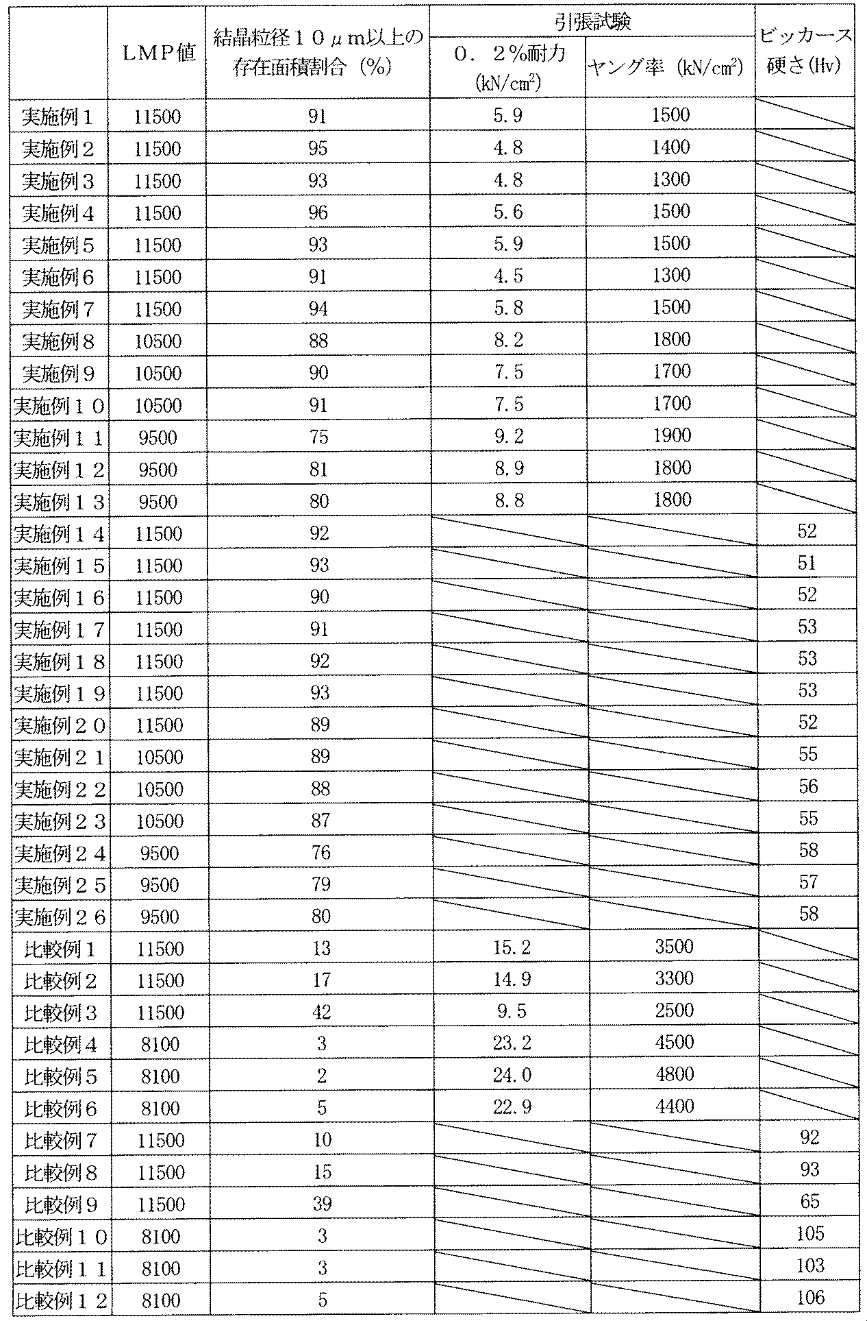
- the electrolytic copper foil prepared above is subjected to a heat treatment in which the LMP value (hereinafter simply referred to as the LMP value) shown in Formula 1 is 9000 or more, the crystal grains having a maximum crystal grain length of 10 ⁇ m or more after the heat treatment are obtained. Is an electrolytic copper foil having a crystal distribution in which 70% or more exists. Furthermore, it is better to perform heat treatment with an LMP value of 11000 or more.
- LMP (T + 273) * (20 + Logt)
- 20 is a material constant of copper
- T temperature (° C.)
- t time (hr).
- FIG. 2 is an example of an electron micrograph of an electrolytic copper foil cross section
- FIG. 2A is a cross sectional photograph of the electrolytic copper foil of the present embodiment
- FIG. 2B is a cross sectional photograph of a conventional electrolytic copper foil.
- the method for measuring the maximum length of crystal grains is to measure the length in the major axis direction of crystal grains in an area of 1000 ⁇ m 2 in a micrograph of an electrolytic copper foil cross section, and the length is occupied by crystal grains having a length of 10 ⁇ m or more. Measure the area by measuring the area and calculating the percentage of the measured area with respect to the entire cross-sectional area.
- the heating 0.2% proof stress of the copper foil after the process performed is less than 10 kN / cm 2 and the Young's modulus is less than 2000 kN / cm 2.
- the 0.2% proof stress is optimally less than 8 kN / cm 2 .
- the present invention can be applied to a copper plating layer provided on a substrate and a copper plating layer provided on a metal wire in a wiring board. That is, the copper plating layer is a thick plating applied after an etching process on a copper laminated substrate, a thick plating after forming a thin layer by sputtering or electroless plating on an organic film, and a copper plating layer is applied to a metal plate or wire.
- the copper plating layer can also be formed with the copper electrolyte of the present invention.
- a copper plating layer is often formed on a metal thin film as described above, it is generally performed under a current density condition lower than that of an electrolytic copper foil.
- the preferable range of the copper concentration, the current density and the electrolyte temperature is 30 to 70 g / l, unlike the electrolytic copper foil, and the preferable range of the current density is 0.1 to 15 A / dm 2.
- the preferable range of the electrolyte temperature is 20 to 50 ° C.
- hardness may be a problem in the copper plating layer, and it is preferable that the hardness is less than 60 Hv when the heat treatment is performed on the copper plating layer.
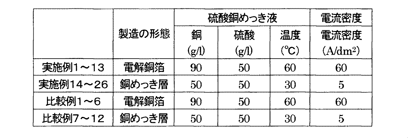
- Examples 14 to 26, Comparative Examples 7 to 12 Similarly, for the copper plating layer, a copper sulfate plating solution having the composition shown in Table 1 is passed through an activated carbon filter and cleaned, and the additives shown in Table 2 are added to obtain a predetermined concentration, followed by the current density shown in Table 1. Then, it was deposited as a copper plating layer having a thickness of 18 ⁇ m on an electroless copper plating layer having a thickness of 1 ⁇ m previously provided on a polyimide film having a thickness of 25 ⁇ m.
- the prepared electrolytic copper foil and copper plating layer were divided into three samples, and one sample was used to measure the amount of impurity elements contained in the sample and the surface roughness. Moreover, it heat-processed using the said unused sample, the observation of a cross-sectional crystal grain, the tensile test in the electrolytic copper foil, and the Vickers hardness test in the copper plating layer were further performed. Finally, using the remaining unused sample, the electrolytic copper foil was thermocompression bonded with the polyimide film, and the copper plating layer was subjected to heat treatment at the same temperature setting, and then subjected to the IPC bending test. Details of each measurement and test are described below.
- the measurement conditions for SIMS analysis are primary ions: Cs + (5 kV, 100 nA) Secondary (detection) ions: Copper (Cu) 63 Cu -- Chlorine (Cl) 35 Cl -- Nitrogen (N) 14 N + 63 Cu -- Sulfur (S) 34 S -- Oxygen (O) 16 O -- Carbon (C) 12 C ⁇ Sputtering area: 200 ⁇ m ⁇ 400 ⁇ m I went there. Since the surfaces of the electrolytic copper foil and the copper plating layer are affected by dirt and oxide film, the measurement was started after sputter removal from the surface to the depth direction of 2 ⁇ m, and the analysis was performed to the depth of 4 ⁇ m. The strength ratio was calculated from the average value of the strength of each measurement element and the average value of the strength of copper.
- FIGS. 3A and 3B An example of the measurement result of the SIMS analysis is shown in FIGS. 3A and 3B, and the calculation result of the intensity ratio is shown in Table 3.
- the amount of impurity elements in the electrolytic copper foil and the copper plating layer in any of the examples is the strength ratio of copper (Cu), chlorine (Cl) is less than 0.5%, and nitrogen (N) is Less than 0.005%, Sulfur (S) is less than 0.005%, Oxygen (O) is less than 1%, Carbon (C) is less than 0.1%, and the surface roughness is Ra: 0. Less than 30 ⁇ m and Rz: less than 2.0 ⁇ m, which is low roughness.
- the ratio of crystal grains having a length of 10 ⁇ m or more (crystal distribution) was 70% or more.
- electrolytic 0.2% proof stress in the copper foil is less than 10 kN / cm 2 and the Young's modulus is less than 2000 kN / cm 2, in the copper plating layer the Vickers hardness is less than 60Hv the conditions of the present invention All were satisfied. Further, as is apparent from Table 5, the electrolytic copper foil and the copper plating layer exhibited good bending characteristics as compared with the comparative example.
- the electrolytic copper foils and copper plating layers of Comparative Examples 1 to 3 and Comparative Examples 7 to 9 have an LMP value of 9000 or more even when satisfactory values are obtained in terms of the amount of impurity elements or surface roughness.
- the proportion of crystal grains having a length of 10 ⁇ m or more (crystal distribution) was less than 70%.
- electrolytic 0.2% proof stress in the copper foil is at 10 kN / cm 2 or more, or a Young's modulus of 2000 kN / cm 2 or more, the copper plating layer Vickers hardness be more 60Hv all satisfy the conditions of the present invention It wasn't something to do.
- the electrolytic copper foil and the copper plating layer exhibited inferior bending characteristics as compared with the Examples.
- the electrolytic copper foils and the copper plating layers of Comparative Examples 4 to 6 and Comparative Examples 10 to 12 have an LMP value of less than 9000 even if satisfactory values are obtained in terms of the amount of impurity elements and surface roughness.
- the ratio of crystal grains having a length of 10 ⁇ m or more (crystal distribution) was less than 70%.
- 0.2% proof stress in the electrodeposited copper foil is at 10 kN / cm 2 or more there and a Young's modulus of 2000 kN / cm 2 or more, in the copper plating layer has a Vickers hardness of more than 60Hv satisfy the conditions of the present invention It wasn't something to do.
- the electrolytic copper film of the present invention, the production method thereof, and the copper electrolyte for producing the copper electrolytic film are printed wiring boards, multilayer printed wiring boards, chip-on-film wiring boards (hereinafter collectively referred to as wiring boards).
- the present invention can be applied to a copper plating layer provided on a substrate, an electrolytic copper film which is a copper plating layer or an electrolytic copper foil provided on a metal wire, a manufacturing method thereof, and a copper electrolyte for producing a copper electrolytic film.
- Anode 2 Cathode 3: Electrolyte 4: Untreated electrolytic copper foil
Landscapes
- Chemical & Material Sciences (AREA)
- Engineering & Computer Science (AREA)
- Chemical Kinetics & Catalysis (AREA)
- Electrochemistry (AREA)
- Materials Engineering (AREA)
- Metallurgy (AREA)
- Organic Chemistry (AREA)
- Microelectronics & Electronic Packaging (AREA)
- Electroplating And Plating Baths Therefor (AREA)
- Electroplating Methods And Accessories (AREA)
Abstract
Description
なお、本明細書において「電解銅皮膜」とは、プリント配線板、多層プリント配線板、チップオンフィルム用配線基板(以下これらを総称して配線板と称することがある)において基板上に設ける銅めっき層、金属線上に施す銅めっき層、電解銅箔を総称する。
屈曲特性を向上させる上で重要な銅箔の特性としては、厚さ・表面平滑性・結晶粒の大きさ・機械的特性などが上げられる。また、電気製品の小型化に対し、高密度配線化が図られるために、できるだけスペースを有効活用することが重要な課題であり、配線板の変形が容易にできるポリイミドフィルムの採用が不可欠となってきており、ポリイミドフィルムに貼り付ける銅箔の接着強度・柔軟性は必要不可欠な特性になってきている。この特性を満足する銅箔としては、特別な製造工程で製箔された圧延銅箔が採用されている。
また配線板においては、回路形成時において厚めっきを行うが、この厚い銅めっき層の形成時にも銅めっき層の柔軟性が要求されている。
しかしながら、現状の銅めっき技術では、電解銅箔の平滑性を維持しながら前記要求を全て満たす電解銅箔及びその製造方法は提案されておらず、上記圧延銅箔と同等またはそれ以上の柔軟性、屈曲性を有する銅電解皮膜(電解銅箔あるいは銅めっき層)は現在のところ存在しない。
式1:LMP=(T+273)*(20+Logt)
ここで、20は銅の材料定数、Tは温度(℃)、tは時間(hr)である。
式1:LMP=(T+273)*(20+Logt)
ここで、20は銅の材料定数、Tは温度(℃)、tは時間(hr)である。
また、本発明は電解銅皮膜を用いた柔軟性、屈曲性を有する配線板を圧延銅箔に比べて安価に提供することができる。
通常電解銅箔は、例えば図1に示すような電解製箔装置により製箔される。電解製箔装置は、回転するドラム状のカソード2(表面はSUS又はチタン製)、該カソード2に対して同心円状に配置されたアノード1(鉛又は貴金属酸化物被覆チタン電極)からなり、該製箔装置に電解液3を供給させつつ両極間に電流を流して該カソード2表面に所定の厚さに銅を電析させ、その後該カソード2表面から銅を箔状に剥ぎ取る。この段階の銅箔を未処理電解銅箔4ということがある。また該未処理電解銅箔4の電解液と接していた面をマット面と呼び回転するドラム状のカソード2と接していた面をシャイニー面と呼ぶ。なお、上記は回転するカソード2を採用した製箔装置につき説明したがカソードを板状とする製箔装置で銅箔を製造することもある。
電解銅箔のシャイニー面の表面粗さRaを0.01μm未満及び/またはRzを0.1μm未満とすることはカソードの研磨技術などを考えると製造が難しく、また量産製造するには不向きであると考えられる。また、シャイニー面の粗さ、Raを0.3μm以上及び/またはRzを2.0μm以上とすると、屈曲特性が非常に悪くなり本発明が求める特性が得られなくなる。
シャイニー面及び/またはマット面の粗さをRa:0.2μm未満、Rz:1.0μm未満とするとなお好適である。
硫酸濃度が20g/l未満となると電流が流れにくくなるので現実的な操業が困難となり、さらにめっきの均一性、電着性も悪くなる。硫酸濃度が150g/lを超えると銅の溶解度が下がるので十分な銅濃度が得られなくなり現実的な操業が困難となる。また、設備の腐食も促進される。
銅濃度が40g/l未満となると電解銅箔の製造において現実的な操業が可能な電流密度を確保することが難しくなる。銅濃度を150g/lより上げるのは相当な高温が必要となり現実的ではない。
塩素濃度は1~100ppm、特に10~50ppmが好ましい。塩素濃度が1ppm未満となると後述する添加剤の効果を出すことが困難となり、100ppmを超えると正常なめっきが困難となる。
上記の電解条件は、それぞれの範囲から、銅の析出、めっきのヤケ等の不具合が起きないような条件に適宜調整して行う。
本発明では、ジ又はポリハロゲン化鎖式脂肪族飽和炭化水素化合物と1又は2以上のエーテル結合を有するジ又はポリハロゲン化鎖式脂肪族飽和炭化水素化合物を組み合わせたものと2個の窒素原子を有するヘテロ環式化合物の反応生成物を用いることも出来る。さらには、上記の原料化合物にジメチルアミン、ジエタノールアミン、エチレンジアミン、等の脂肪族アミノ化合物、フェニレンジアミン等の芳香族アミノ化合物、スクシニルクロリド、グルタリルクロリド、フマリルクロリド、ジクロロキシリレン、フタロイルクロリド等の複数の反応性基を有する化合物を第三原料として加えて反応した生成物を用いることもできる。但し、エピクロロヒドリン等のエピハロヒドリンを第三反応成分に用いることは反応生成物の所期の効果が得られないという点で好ましくない。
式1:LMP=(T+273)*(20+Logt)
ここで、20は銅の材料定数、Tは温度(℃)、tは時間(hr)である。
結晶粒の最大長さの測定方法は電解銅箔断面を撮影した顕微鏡写真の、1000μm2の面積において結晶粒の長軸方向の長さを計測し,その長さが10μm以上の結晶粒の占める面積を測定し,測定した面積が断面全体の面積に対して何%であるかを算出する方法で測定する。
即ち、上記銅めっき層は銅積層基板におけるエッチング処理後に施す厚めっき、有機フィルム上にスパッタリング、無電解めっきにて薄層を形成した後の厚めっき、金属板、線に銅めっき層を施す、銅めっき層についても本発明の銅電解液で製膜することが可能である。
なお、銅めっき層は上記のように金属薄膜上に製膜される場合が多いため電解銅箔と比較して一般的に低い電流密度条件で行う。そのため、銅濃度、電流密度、電解液温の好適な範囲は電解銅箔とは異なり銅濃度の好ましい範囲が30~70g/lであり、電流密度の好ましい範囲が0.1~15A/dm2であり、電解液温の好ましい範囲が20~50℃である。
また、銅めっき層においては硬度が問題となる場合があるが、該硬度は銅めっき層に対し上記加熱処理を行なった場合のビッカース硬さが60Hv未満であることが好ましい。
以下に本発明を実施例に基づいて説明するが、本発明はこれらに限定されるものではない。
実施例1~13、比較例1~6
電解液組成を表1に示す。電解銅箔については表1に示す組成の硫酸銅めっき液(以下電解液ということもある)を活性炭フィルターに通して清浄処理し、表2に示す添加剤を添加し所定の濃度とした後、表1に示す電流密度で、図1に示すチタン製の回転ドラム上に厚さ18μmの電解銅箔として析出させた後、剥離して巻き取った。
実施例14~26、比較例7~12
同様に、銅めっき層については表1に示す組成の硫酸銅めっき液を活性炭フィルターに通して清浄処理し、表2に示す添加剤を添加し所定の濃度とした後、表1に示す電流密度で、厚さ25μmのポリイミドフィルム上にあらかじめ設けた厚さ1μmの無電解銅めっき層上に厚さ18μmの銅めっき層として析出させた。
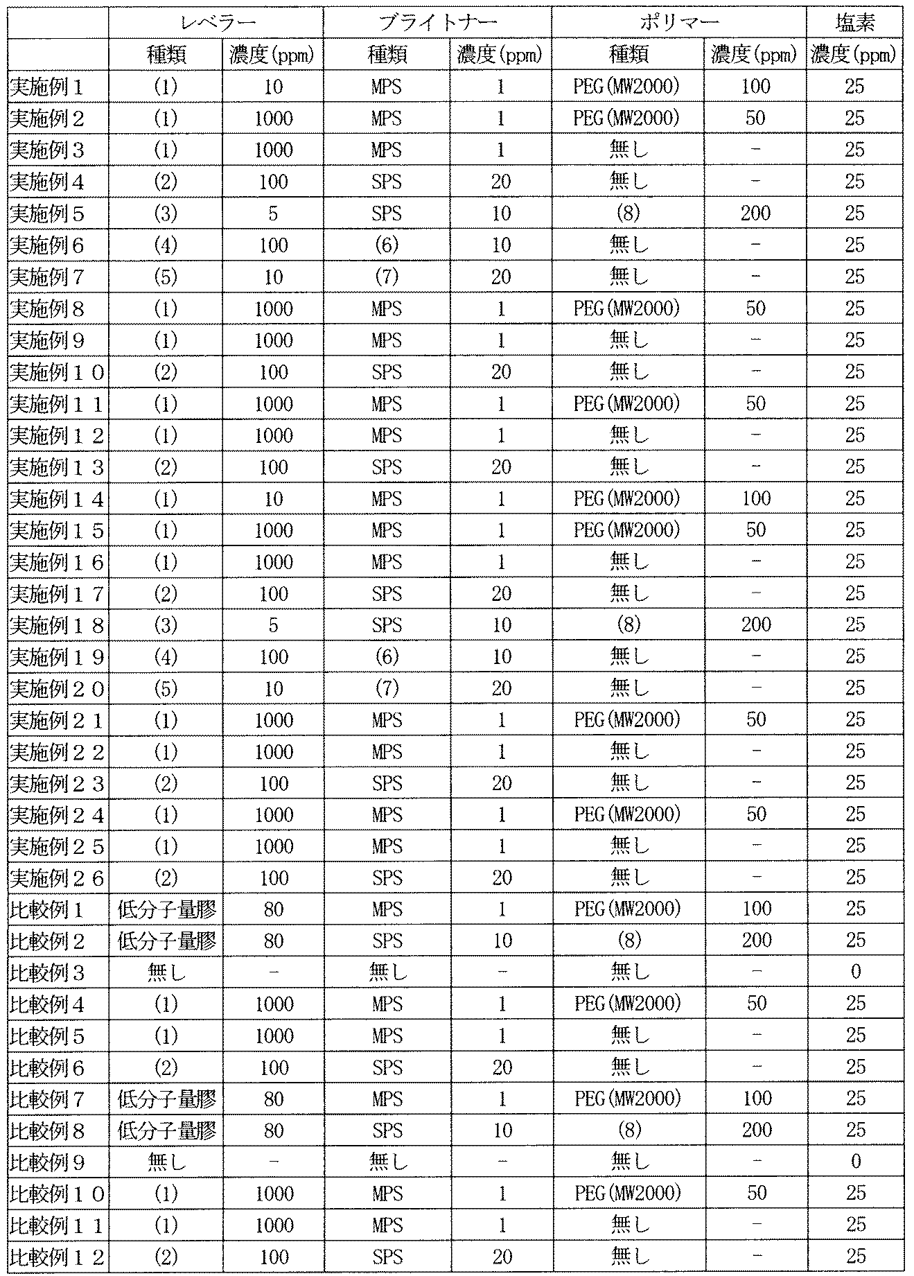
レベラー
(1) :1,4-ジクロロ-2-ブタノールと2-ピラゾリンの反応生成物
(2) :2,2'-ジクロロエチルエーテルと2-イミダゾリンの反応生成物
(3) :1,3-ジクロロ-2-プロパノールとイミダゾールの反応生成物
(4) :1,3-ジクロロプロパンと2-メチル-2-イミダゾリンの反応生成物
(5) :1,3-ジブロモプロパンとピペラジンの反応生成物
ブライトナー
MPS :3-メルカプトプロパンスルホン酸ナトリウム
SPS :ビス(3-スルホプロピル)ジスルフィドナトリウム
(6) :N,N-ジメチルジチオカルバミン酸ナトリウム
(7) :3-(ベンゾチアゾリル-2-チオ)プロピルスルホン酸ナトリウム
ポリマー
PEG :ポリエチレングリコール(分子量2000)
(8) :ポリエチレングリコール-ポリプロピレングリコール共重合体
実施例1~7、実施例14~20、比較例1~3、比較例7~9の電解銅箔と銅めっき層の内部の不純物元素量をSIMS分析において深さ方向に掘って測定した。測定元素は酸素(O)、炭素(C)、塩素(Cl),窒素(N)、硫黄(S)である。SIMS分析の測定条件は
1次イオン :Cs+(5kV,100nA)
2次(検出)イオン :銅(Cu)63Cu-・塩素(Cl)35Cl-・窒素(N)14N+63Cu-・硫黄(S)34S-・酸素(O)16O-・炭素(C)12C-
スパッタ領域 :200μm×400μm
で行った。電解銅箔と銅めっき層の表面は汚れや酸化被膜の影響があるので表面から深さ方向2μmまでスパッタ除去した後に測定を開始し、深さ4μmまで分析を行った。各測定元素の強度の平均値と銅の強度の平均値から強度比を算出した。SIMS分析の測定結果の一例を図3A及び図3Bに、強度比の算出結果を表3に記載する。
実施例1~7、実施例14~20、比較例1~3、比較例7~9の電解銅箔と銅めっき層の表面粗さRa、Rzを接触式表面粗さ計を用いて測定した。表面粗さはJIS-B-0601に規定されるRa(算術平均粗さ)、Rz(十点平均粗さ)で示している。基準長さは0.8mmで行った。電解銅箔についてはマット面とシャイニー面にて、銅めっき層については銅めっき層表面とめっき前の無電解銅層表面にて測定を行った。表面粗さ測定の結果を表3に記載する。
実施例1~7、実施例14~20、比較例1~3、比較例7~9の電解銅箔と銅めっき層を前記式1のLMP値が9000以上となる300℃、1時間の加熱条件(LMP値=11500)で、窒素雰囲気中で加熱処理を行った。同様に実施例8~10、実施例21~23の電解銅箔と銅めっき層についてはLMP値が9000以上となる250℃、1時間の加熱条件(LMP値=10500)で、窒素雰囲気中で加熱処理を行った。さらに、実施例11~13、実施例24~26の電解銅箔と銅めっき層についてはLMP値が9000以上となる200℃、1時間の加熱条件(LMP値=9500)で、窒素雰囲気中で加熱処理を行った。最後に、比較例4~6、比較例10~12の電解銅箔と銅めっき層についてはLMP値が9000未満となる130℃、1時間の加熱条件(LMP値=8100)で、窒素雰囲気中で加熱処理を行った。
各実施例及び各比較例の電解銅箔と銅めっき層を前記加熱条件で加熱処理した後、銅皮膜の断面を電子顕微鏡で撮影し、1000μm2の範囲で結晶粒の最大長さが10μm以上の結晶が占める割合を測定・算出した。断面結晶粒の観察結果を表4に記載する。
実施例1~13、比較例1~6の電解銅箔を前記加熱条件で加熱処理した後、長さ6インチ×幅0.5インチの試験片に裁断し引張試験機を用いて0.2%耐力、及びヤング率を測定した。尚、引張速度は50mm/minとした。引張試験結果を表4に記載する。
0.2%耐力とは、歪と応力の関係曲線において、歪が0%の点において曲線に接線を引き、その接線と平行に歪が0.2%の点に直線を引いたその直線と曲線が交った点の応力を断面積で割ったものである。
実施例14~26、比較例7~12の銅めっき層を前記加熱条件で加熱処理した後、樹脂に埋め込み断面をカット後研磨してビッカース硬さ試験機を用いて測定した。なお、荷重は10gf、荷重保持時間は15secとした。ビッカース硬さ試験結果を表4に記載する。
実施例1~7、比較例1~3の電解銅箔と厚さ25μmのポリイミドフィルムを330℃、20分間の加熱条件(LMP値=11800)でプレス圧着してポリイミドフィルム貼付電解銅箔を作成した。さらに実施例14~20、比較例7~9の厚さ25μmのポリイミドフィルム上の銅めっき層も同様に330℃、20分間の熱条件(LMP値=11800)で加熱処理した。得られたポリイミドフィルム貼付電解銅箔及び銅めっき層を図4Aに示す回路パターンにエッチングし、同じく図4Bに示すように通電部を残して回路形成面に厚さ25μmのポリイミドカバーフィルムを300℃、20分間の加熱条件(LMP値=11200)でプレス圧着してIPC屈曲試験サンプルを得た。得られた試験サンプルを下記の条件にてIPC屈曲試験を行い初期状態からの電気抵抗の増加率を測定した。IPC屈曲試験結果を表5に記載する。
試験装置 :信越エンジニアリング(株)製 SEK-31B2S
屈曲半径 :2.0mm
振動ストローク幅 :20mm
屈曲速度 :1500回/分

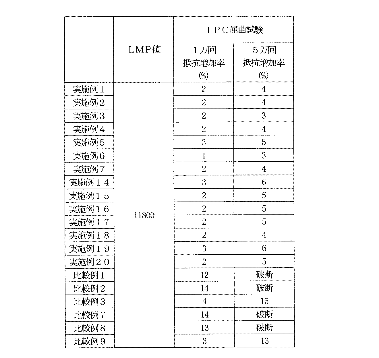
さらに、表5から明らかなように該電解銅箔と銅めっき層は比較例と比較して良好な屈曲特性を示した。
さらに、表5から明らかなように該電解銅箔と銅めっき層は実施例と比較して劣る屈曲特性を示した。
2:カソード
3:電解液
4:未処理電解銅箔
Claims (12)
- 電解析出で製造した電解銅皮膜において、式1に示すLMP(Larson-Miller parameter)値が9000以上となる加熱処理を施すと、加熱処理後の結晶粒の最大長さが10μm以上となる結晶粒子が70%以上存在する結晶分布となる電解銅皮膜。
式1:LMP=(T+273)*(20+Logt)
ここで、20は銅の材料定数、Tは温度(℃)、tは時間(hr)である。 - 前記LMP値が9000以上となる加熱処理を施すと、0.2%耐力が10kN/cm2未満となり、かつヤング率が2000kN/cm2未満となることを特徴とする請求項1に記載の電解銅皮膜。
- 前記LMP値が9000以上となる加熱処理を施すと、ビッカース硬さが60Hv未満となることを特徴とする請求項1に記載の電解銅皮膜。
- 前記電解銅皮膜は、銅皮膜深さ方向のSIMS(Secondary Ion Mass Spectrometry)分析における銅(Cu)との強度比で少なくとも塩素(Cl)は0.5%未満、窒素(N)は0.005%未満、硫黄(S)は0.005%未満であることを特徴とする請求項1~3のいずれかに記載の電解銅皮膜。
- 前記電解銅皮膜の少なくとも片方の表面粗さが、Ra:0.30μm未満、Rz:2.0μm未満であることを特徴とする請求項1~4のいずれかに記載の電解銅皮膜。
- 銅電解液にて電解析出した銅めっき皮膜に、式1に示すLMP値が9000以上となる加熱処理を施すと、加熱処理後の結晶粒の最大長さが10μm以上である結晶粒子が70%以上存在する結晶分布となる電解銅皮膜の製造方法。
式1:LMP=(T+273)*(20+Logt)
ここで、20は銅の材料定数、Tは温度(℃)、tは時間(hr)である。 - ジ又はポリハロゲン化鎖式脂肪族飽和炭化水素化合物の一種以上もしくは1又は2以上のエーテル結合を有するジ又はポリハロゲン化鎖式脂肪族飽和炭化水素化合物の一種以上、又はジ又はポリハロゲン化鎖式脂肪族飽和炭化水素化合物の一種以上と1又は2以上のエーテル結合を有するジ又はポリハロゲン化鎖式脂肪族飽和炭化水素化合物の一種以上を組み合わせたものと、2個の窒素原子を有するヘテロ環式化合物との反応生成物の一種以上が含有されていることを特徴とする前記銅電解液を用いた請求項6に記載の電解銅皮膜の製造方法。
- ジ又はポリハロゲン化鎖式脂肪族飽和炭化水素化合物の一種以上もしくは1又は2以上のエーテル結合を有するジ又はポリハロゲン化鎖式脂肪族飽和炭化水素化合物の一種以上、又はジ又はポリハロゲン化鎖式脂肪族飽和炭化水素化合物の一種以上と1又は2以上のエーテル結合を有するジ又はポリハロゲン化鎖式脂肪族飽和炭化水素化合物の一種以上を組み合わせたものと、2個の窒素原子を有するヘテロ環式化合物との反応生成物の一種以上、及びブライトナーの一種以上が含有されていることを特徴とする前記銅電解液を用いた請求項6又は7に記載の電解銅皮膜の製造方法。
- 2個の窒素原子を有するヘテロ環式化合物が2個の窒素原子を有するヘテロ環式芳香族化合物であることを特徴とする前記銅電解液を用いた請求項6~8のいずれかに記載の電解銅皮膜の製造方法。
- ジ又はポリハロゲン化鎖式脂肪族飽和炭化水素化合物もしくは1又は2以上のエーテル結合を有するジ又はポリハロゲン化鎖式脂肪族飽和炭化水素化合物と、2個の窒素原子を有するヘテロ環式化合物との反応生成物の一種以上、及びブライトナーの一種以上が含有されていることを特徴とする電解銅皮膜製造用の銅電解液。
- ジ又はポリハロゲン化鎖式脂肪族飽和炭化水素化合物の一種以上もしくは1又は2以上のエーテル結合を有するジ又はポリハロゲン化鎖式脂肪族飽和炭化水素化合物の一種以上、又はジ又はポリハロゲン化鎖式脂肪族飽和炭化水素化合物の一種以上と1又は2以上のエーテル結合を有するジ又はポリハロゲン化鎖式脂肪族飽和炭化水素化合物の一種以上を組み合わせたものと、2個の窒素原子を有するヘテロ環式化合物との反応生成物の一種以上が含有されていることを特徴とする電解銅皮膜製造用の銅電解液。
- ジ又はポリハロゲン化鎖式脂肪族飽和炭化水素化合物の一種以上もしくは1又は2以上のエーテル結合を有するジ又はポリハロゲン化鎖式脂肪族飽和炭化水素化合物の一種以上、又はジ又はポリハロゲン化鎖式脂肪族飽和炭化水素化合物の一種以上と1又は2以上のエーテル結合を有するジ又はポリハロゲン化鎖式脂肪族飽和炭化水素化合物の一種以上を組み合わせたものと、2個の窒素原子を有するヘテロ環式化合物との反応生成物の一種以上、及びブライトナーの一種以上が含有されていることを特徴とする電解銅皮膜製造用の銅電解液。
Priority Applications (4)
| Application Number | Priority Date | Filing Date | Title |
|---|---|---|---|
| CN2009801302754A CN102105622A (zh) | 2008-06-12 | 2009-06-12 | 电解铜涂层及其制造方法,用于制造电解铜涂层的铜电解液 |
| KR1020117000332A KR101274544B1 (ko) | 2008-06-12 | 2009-06-12 | 전해 동피막, 그 제조 방법 및 동전해 피막 제조용의 동 전해액 |
| US12/997,420 US20110139626A1 (en) | 2008-06-12 | 2009-06-12 | Electrolytic copper coating, method of manufacturing the same, and copper electrolyte for manufacturing electrolytic copper coating |
| EP09762554.5A EP2302103A4 (en) | 2008-06-12 | 2009-06-12 | ELECTROLYTE COPPER COATING AND PRODUCTION METHOD AND COPPER ELECTROLYTE FOR THE PRODUCTION OF ELECTROLYTE COPPER COATINGS |
Applications Claiming Priority (2)
| Application Number | Priority Date | Filing Date | Title |
|---|---|---|---|
| JP2008-154025 | 2008-06-12 | ||
| JP2008154025 | 2008-06-12 |
Publications (1)
| Publication Number | Publication Date |
|---|---|
| WO2009151124A1 true WO2009151124A1 (ja) | 2009-12-17 |
Family
ID=41416826
Family Applications (1)
| Application Number | Title | Priority Date | Filing Date |
|---|---|---|---|
| PCT/JP2009/060792 Ceased WO2009151124A1 (ja) | 2008-06-12 | 2009-06-12 | 電解銅皮膜、その製造方法及び銅電解皮膜製造用の銅電解液 |
Country Status (6)
| Country | Link |
|---|---|
| US (1) | US20110139626A1 (ja) |
| EP (1) | EP2302103A4 (ja) |
| JP (1) | JP2010018885A (ja) |
| KR (1) | KR101274544B1 (ja) |
| CN (1) | CN102105622A (ja) |
| WO (1) | WO2009151124A1 (ja) |
Cited By (5)
| Publication number | Priority date | Publication date | Assignee | Title |
|---|---|---|---|---|
| US20130161614A1 (en) * | 2010-07-30 | 2013-06-27 | Ashutosh Tiwari | Nanostructured films and related methods |
| EP2654111A4 (en) * | 2010-12-27 | 2014-08-13 | Furukawa Electric Co Ltd | LITHIUMION SECONDARY BATTERY, ELECTRODE FOR SECONDARY BATTERY AND ELECTROLYTIC COPPER FOIL FOR SECONDARY BATTERY ELECTRODE |
| JP2014198885A (ja) * | 2013-03-29 | 2014-10-23 | Jx日鉱日石金属株式会社 | 電解銅箔、それを用いた銅張積層体、プリント配線板及び電子部品 |
| JP2019052374A (ja) * | 2010-03-15 | 2019-04-04 | ローム アンド ハース エレクトロニック マテリアルズ エルエルシーRohm and Haas Electronic Materials LLC | めっき浴および方法 |
| JP2023154854A (ja) * | 2022-04-08 | 2023-10-20 | 日本電解株式会社 | 電解銅箔およびその製造方法 |
Families Citing this family (24)
| Publication number | Priority date | Publication date | Assignee | Title |
|---|---|---|---|---|
| WO2010004988A1 (ja) * | 2008-07-07 | 2010-01-14 | 古河電気工業株式会社 | 電解銅箔および銅張積層板 |
| JP5794806B2 (ja) * | 2011-03-30 | 2015-10-14 | 古河電気工業株式会社 | 表面処理銅箔、および、該表面処理銅箔を用いた銅張積層基板、並びにプリント配線基板 |
| US8747643B2 (en) * | 2011-08-22 | 2014-06-10 | Rohm And Haas Electronic Materials Llc | Plating bath and method |
| JP5730742B2 (ja) * | 2011-10-25 | 2015-06-10 | 古河電気工業株式会社 | リチウムイオン二次電池用電解銅箔とその製造方法 |
| CN103074646A (zh) * | 2013-01-11 | 2013-05-01 | 安徽铜冠铜箔有限公司 | 一种钛辊表面铜箔收卷方式 |
| TWI539032B (zh) * | 2013-08-01 | 2016-06-21 | Chang Chun Petrochemical Co | Electrolytic copper foil, cleaning fluid composition and cleaning copper foil method |
| JP5810197B2 (ja) * | 2013-09-11 | 2015-11-11 | 古河電気工業株式会社 | 電解銅箔、フレキシブル配線板及び電池 |
| US9403762B2 (en) | 2013-11-21 | 2016-08-02 | Rohm And Haas Electronic Materials Llc | Reaction products of guanidine compounds or salts thereof, polyepoxides and polyhalogens |
| JP6260860B2 (ja) * | 2013-12-27 | 2018-01-17 | 日立金属株式会社 | 電解アルミニウム箔、それを用いた電池用電極、及び蓄電デバイス、並びに電解アルミニウム箔の製造方法 |
| TWI710671B (zh) * | 2014-09-15 | 2020-11-21 | 美商麥德美樂思公司 | 微電子技術中銅沈積用之平整劑 |
| JP6421719B2 (ja) * | 2015-07-31 | 2018-11-14 | 住友金属鉱山株式会社 | フレキシブル配線板用の電気銅めっき液及び該電気銅めっき液により製造される積層体の製造方法 |
| CN105483764B (zh) * | 2015-12-04 | 2019-02-22 | 广东嘉元科技股份有限公司 | 一种电解铜箔添加剂 |
| US10749278B2 (en) * | 2016-01-15 | 2020-08-18 | Taiwan Semiconductor Manufacturing Co., Ltd. | Method of electroplating metal into recessed feature and electroplating layer in recessed feature |
| JP6834070B2 (ja) * | 2016-06-13 | 2021-02-24 | 石原ケミカル株式会社 | 電気スズ及びスズ合金メッキ浴、当該メッキ浴を用いて電着物を形成した電子部品の製造方法 |
| WO2018207785A1 (ja) * | 2017-05-09 | 2018-11-15 | Jx金属株式会社 | 電解銅箔及びその製造方法、銅張積層板、プリント配線板及びその製造方法、並びに電子機器及びその製造方法 |
| TW201900939A (zh) * | 2017-05-09 | 2019-01-01 | 日商Jx金屬股份有限公司 | 電解銅箔、覆銅積層板、印刷配線板及其製造方法、以及電子機器及其製造方法 |
| WO2018207788A1 (ja) * | 2017-05-09 | 2018-11-15 | Jx金属株式会社 | 電解銅箔及びその製造方法、銅張積層板、プリント配線板及びその製造方法、並びに電子機器及びその製造方法 |
| WO2019024973A1 (en) * | 2017-07-31 | 2019-02-07 | Circuit Foil Luxembourg, Sàrl | SURFACE TREATED COPPER FOIL AND COPPER LAMINATE |
| KR102302184B1 (ko) * | 2018-02-01 | 2021-09-13 | 에스케이넥실리스 주식회사 | 고온 치수 안정성 및 집합조직 안정성을 갖는 전해동박 및 그 제조방법 |
| TWI705160B (zh) | 2019-12-09 | 2020-09-21 | 長春石油化學股份有限公司 | 電解銅箔、包含其的電極和覆銅積層板 |
| TWI715424B (zh) | 2020-01-22 | 2021-01-01 | 長春石油化學股份有限公司 | 電解銅箔、電極及包含其之鋰離子電池 |
| CN114073170B (zh) * | 2020-04-01 | 2025-01-03 | 住友电气工业株式会社 | 柔性印刷布线板及其制造方法 |
| WO2024016330A1 (zh) * | 2022-07-22 | 2024-01-25 | 扬州纳力新材料科技有限公司 | 无氰镀铜晶粒细化剂、无氰镀铜镀液及其配制方法、应用 |
| CN115287715B (zh) * | 2022-08-25 | 2023-06-23 | 广东盈华电子科技有限公司 | 一种中抗拉强度锂电池用双光铜箔的生产工艺 |
Citations (6)
| Publication number | Priority date | Publication date | Assignee | Title |
|---|---|---|---|---|
| JPS527819A (en) * | 1975-07-10 | 1977-01-21 | Furukawa Electric Co Ltd:The | Process for smooth electrodeposition of copper |
| JP2004035918A (ja) * | 2002-07-01 | 2004-02-05 | Nippon Denkai Kk | 電解銅箔の製造方法 |
| WO2004059040A1 (ja) * | 2002-12-25 | 2004-07-15 | Nikko Materials Co., Ltd. | 特定骨格を有する四級アミン化合物重合体及び有機硫黄化合物を添加剤として含む銅電解液並びにそれにより製造される電解銅箔 |
| JP2004250777A (ja) * | 2002-06-03 | 2004-09-09 | Shipley Co Llc | レベラー化合物 |
| JP2006057177A (ja) * | 2004-07-23 | 2006-03-02 | C Uyemura & Co Ltd | 電気銅めっき浴及び電気銅めっき方法 |
| JP2007146289A (ja) * | 2005-10-31 | 2007-06-14 | Mitsui Mining & Smelting Co Ltd | 電解銅箔の製造方法、該製造方法で得られる電解銅箔、該電解銅箔を用いて得られる表面処理銅箔及び該電解銅箔又は該表面処理銅箔を用いて得られる銅張積層板 |
Family Cites Families (7)
| Publication number | Priority date | Publication date | Assignee | Title |
|---|---|---|---|---|
| US4038161A (en) * | 1976-03-05 | 1977-07-26 | R. O. Hull & Company, Inc. | Acid copper plating and additive composition therefor |
| LU90532B1 (en) * | 2000-02-24 | 2001-08-27 | Circuit Foil Luxembourg Trading Sarl | Comosite copper foil and manufacturing method thereof |
| JP3520034B2 (ja) * | 2000-07-25 | 2004-04-19 | 古河電気工業株式会社 | 電子電気機器部品用銅合金材 |
| AU2002330396A1 (en) * | 2002-09-12 | 2004-04-30 | Matsushita Electric Industrial Co., Ltd. | Metal foil for current collector of secondary battery and method for producing the same |
| TW200613586A (en) * | 2004-07-22 | 2006-05-01 | Rohm & Haas Elect Mat | Leveler compounds |
| JP4712759B2 (ja) * | 2006-06-07 | 2011-06-29 | 古河電気工業株式会社 | 表面処理電解銅箔及びその製造方法、並びに回路基板 |
| CN101669237A (zh) * | 2007-04-20 | 2010-03-10 | 日矿金属株式会社 | 锂二次电池用电解铜箔及该铜箔的制造方法 |
-
2009
- 2009-06-12 KR KR1020117000332A patent/KR101274544B1/ko active Active
- 2009-06-12 CN CN2009801302754A patent/CN102105622A/zh active Pending
- 2009-06-12 US US12/997,420 patent/US20110139626A1/en not_active Abandoned
- 2009-06-12 EP EP09762554.5A patent/EP2302103A4/en not_active Withdrawn
- 2009-06-12 WO PCT/JP2009/060792 patent/WO2009151124A1/ja not_active Ceased
- 2009-06-12 JP JP2009141216A patent/JP2010018885A/ja active Pending
Patent Citations (6)
| Publication number | Priority date | Publication date | Assignee | Title |
|---|---|---|---|---|
| JPS527819A (en) * | 1975-07-10 | 1977-01-21 | Furukawa Electric Co Ltd:The | Process for smooth electrodeposition of copper |
| JP2004250777A (ja) * | 2002-06-03 | 2004-09-09 | Shipley Co Llc | レベラー化合物 |
| JP2004035918A (ja) * | 2002-07-01 | 2004-02-05 | Nippon Denkai Kk | 電解銅箔の製造方法 |
| WO2004059040A1 (ja) * | 2002-12-25 | 2004-07-15 | Nikko Materials Co., Ltd. | 特定骨格を有する四級アミン化合物重合体及び有機硫黄化合物を添加剤として含む銅電解液並びにそれにより製造される電解銅箔 |
| JP2006057177A (ja) * | 2004-07-23 | 2006-03-02 | C Uyemura & Co Ltd | 電気銅めっき浴及び電気銅めっき方法 |
| JP2007146289A (ja) * | 2005-10-31 | 2007-06-14 | Mitsui Mining & Smelting Co Ltd | 電解銅箔の製造方法、該製造方法で得られる電解銅箔、該電解銅箔を用いて得られる表面処理銅箔及び該電解銅箔又は該表面処理銅箔を用いて得られる銅張積層板 |
Cited By (7)
| Publication number | Priority date | Publication date | Assignee | Title |
|---|---|---|---|---|
| JP2019052374A (ja) * | 2010-03-15 | 2019-04-04 | ローム アンド ハース エレクトロニック マテリアルズ エルエルシーRohm and Haas Electronic Materials LLC | めっき浴および方法 |
| US20130161614A1 (en) * | 2010-07-30 | 2013-06-27 | Ashutosh Tiwari | Nanostructured films and related methods |
| US9057144B2 (en) * | 2010-07-30 | 2015-06-16 | University Of Utah Research Foundation | Nanostructured films and related methods |
| EP2654111A4 (en) * | 2010-12-27 | 2014-08-13 | Furukawa Electric Co Ltd | LITHIUMION SECONDARY BATTERY, ELECTRODE FOR SECONDARY BATTERY AND ELECTROLYTIC COPPER FOIL FOR SECONDARY BATTERY ELECTRODE |
| US9603245B2 (en) | 2010-12-27 | 2017-03-21 | Furukawa Electric Co., Ltd. | Lithium-ion secondary battery, electrode for the secondary battery, and electrolytic copper foil for electrode for the secondary battery |
| JP2014198885A (ja) * | 2013-03-29 | 2014-10-23 | Jx日鉱日石金属株式会社 | 電解銅箔、それを用いた銅張積層体、プリント配線板及び電子部品 |
| JP2023154854A (ja) * | 2022-04-08 | 2023-10-20 | 日本電解株式会社 | 電解銅箔およびその製造方法 |
Also Published As
| Publication number | Publication date |
|---|---|
| KR20110017429A (ko) | 2011-02-21 |
| JP2010018885A (ja) | 2010-01-28 |
| US20110139626A1 (en) | 2011-06-16 |
| CN102105622A (zh) | 2011-06-22 |
| EP2302103A1 (en) | 2011-03-30 |
| EP2302103A4 (en) | 2014-05-28 |
| KR101274544B1 (ko) | 2013-06-17 |
Similar Documents
| Publication | Publication Date | Title |
|---|---|---|
| WO2009151124A1 (ja) | 電解銅皮膜、その製造方法及び銅電解皮膜製造用の銅電解液 | |
| JP4827952B2 (ja) | 電解銅箔および銅張積層板 | |
| JP5255229B2 (ja) | 電解銅箔、その電解銅箔を用いた表面処理銅箔及びその表面処理銅箔を用いた銅張積層板並びにその電解銅箔の製造方法 | |
| KR101154203B1 (ko) | 전해 동박, 그 전해 동박을 이용한 표면 처리 동박 및 그 표면 처리 동박을 이용한 동박 적층판 및 그 전해 동박의 제조 방법 | |
| JP5391366B2 (ja) | 電解銅箔、該電解銅箔を使用した配線板及びフレキシブル配線板 | |
| JP3058445B2 (ja) | 特性の調整された、印刷回路基板用の電着された箔並びにそれを製造するための方法及び電解槽溶液 | |
| TWI509111B (zh) | Surface treatment of electrolytic copper foil, laminated board, and printed wiring board, electronic equipment | |
| JP6014186B2 (ja) | 電解銅箔、これを含む電気部品および電池 | |
| JP5752301B2 (ja) | 電解銅箔及びその電解銅箔の製造方法 | |
| JP2018141230A (ja) | 電解液、電解銅箔及びその製造方法 | |
| JP2009299100A (ja) | 電解銅箔及びその電解銅箔の製造方法 | |
| WO2014104233A1 (ja) | 低反発性電解銅箔、該電解銅箔を使用した配線板及びフレキシブル配線板 | |
| CN1946879B (zh) | 作为添加剂含有具有特定骨架化合物的铜电解液以及由该铜电解液制造的电解铜箔 | |
| JPS63310990A (ja) | 電解銅箔の製造方法 | |
| KR102323903B1 (ko) | 연성인쇄회로기판의 치수안정성을 향상시킬 수 있는 동박, 그 제조방법, 및 그것을 포함하는 연성동박적층필름 | |
| KR101126969B1 (ko) | 고굴곡성의 전해 동박 및 그 제조 방법 | |
| TWI465609B (zh) | An electrolytic copper film, a method for producing the same, and a copper electrolytic solution for manufacturing a copper electrolytic film | |
| EP4202084A2 (en) | Double layered electrolytic copper foil and manufacturing method thereof | |
| TWI647096B (zh) | 表面處理銅箔及其製造方法 | |
| KR101224034B1 (ko) | 인쇄회로용 동박 및 그 제조방법 | |
| KR102432584B1 (ko) | 비전도성 고분자막과의 박리강도를 향상시킬 수 있는 동박, 그 제조방법, 및 그것을 포함하는 연성동박적층필름 | |
| KR20180113832A (ko) | 양호한 방청 성능을 갖는 연성동박적층판 및 연성동박적층판의 시험 방법 | |
| KR20110045952A (ko) | 내굴곡성이 향상된 연성회로기판용 적층 구조체의 제조방법 및 이 방법에 의해 제조된 적층 구조체 | |
| TWM543879U (zh) | 電解銅箔及應用其的電氣組件 |
Legal Events
| Date | Code | Title | Description |
|---|---|---|---|
| WWE | Wipo information: entry into national phase |
Ref document number: 200980130275.4 Country of ref document: CN |
|
| 121 | Ep: the epo has been informed by wipo that ep was designated in this application |
Ref document number: 09762554 Country of ref document: EP Kind code of ref document: A1 |
|
| NENP | Non-entry into the national phase |
Ref country code: DE |
|
| ENP | Entry into the national phase |
Ref document number: 20117000332 Country of ref document: KR Kind code of ref document: A |
|
| WWE | Wipo information: entry into national phase |
Ref document number: 2009762554 Country of ref document: EP |
|
| WWE | Wipo information: entry into national phase |
Ref document number: 12997420 Country of ref document: US |