WO2009157456A1 - 電気電子部品用複合材料およびそれを用いた電気電子部品 - Google Patents
電気電子部品用複合材料およびそれを用いた電気電子部品 Download PDFInfo
- Publication number
- WO2009157456A1 WO2009157456A1 PCT/JP2009/061429 JP2009061429W WO2009157456A1 WO 2009157456 A1 WO2009157456 A1 WO 2009157456A1 JP 2009061429 W JP2009061429 W JP 2009061429W WO 2009157456 A1 WO2009157456 A1 WO 2009157456A1
- Authority
- WO
- WIPO (PCT)
- Prior art keywords
- metal layer
- electrical
- insulating film
- plating
- composite material
- Prior art date
- Legal status (The legal status is an assumption and is not a legal conclusion. Google has not performed a legal analysis and makes no representation as to the accuracy of the status listed.)
- Ceased
Links
Images

Classifications
-
- C—CHEMISTRY; METALLURGY
- C25—ELECTROLYTIC OR ELECTROPHORETIC PROCESSES; APPARATUS THEREFOR
- C25D—PROCESSES FOR THE ELECTROLYTIC OR ELECTROPHORETIC PRODUCTION OF COATINGS; ELECTROFORMING; APPARATUS THEREFOR
- C25D5/00—Electroplating characterised by the process; Pretreatment or after-treatment of workpieces
- C25D5/48—After-treatment of electroplated surfaces
- C25D5/50—After-treatment of electroplated surfaces by heat-treatment
-
- B—PERFORMING OPERATIONS; TRANSPORTING
- B05—SPRAYING OR ATOMISING IN GENERAL; APPLYING FLUENT MATERIALS TO SURFACES, IN GENERAL
- B05D—PROCESSES FOR APPLYING FLUENT MATERIALS TO SURFACES, IN GENERAL
- B05D7/00—Processes, other than flocking, specially adapted for applying liquids or other fluent materials to particular surfaces or for applying particular liquids or other fluent materials
- B05D7/14—Processes, other than flocking, specially adapted for applying liquids or other fluent materials to particular surfaces or for applying particular liquids or other fluent materials to metal, e.g. car bodies
- B05D7/16—Processes, other than flocking, specially adapted for applying liquids or other fluent materials to particular surfaces or for applying particular liquids or other fluent materials to metal, e.g. car bodies using synthetic lacquers or varnishes
-
- C—CHEMISTRY; METALLURGY
- C22—METALLURGY; FERROUS OR NON-FERROUS ALLOYS; TREATMENT OF ALLOYS OR NON-FERROUS METALS
- C22C—ALLOYS
- C22C19/00—Alloys based on nickel or cobalt
- C22C19/03—Alloys based on nickel or cobalt based on nickel
-
- C—CHEMISTRY; METALLURGY
- C23—COATING METALLIC MATERIAL; COATING MATERIAL WITH METALLIC MATERIAL; CHEMICAL SURFACE TREATMENT; DIFFUSION TREATMENT OF METALLIC MATERIAL; COATING BY VACUUM EVAPORATION, BY SPUTTERING, BY ION IMPLANTATION OR BY CHEMICAL VAPOUR DEPOSITION, IN GENERAL; INHIBITING CORROSION OF METALLIC MATERIAL OR INCRUSTATION IN GENERAL
- C23C—COATING METALLIC MATERIAL; COATING MATERIAL WITH METALLIC MATERIAL; SURFACE TREATMENT OF METALLIC MATERIAL BY DIFFUSION INTO THE SURFACE, BY CHEMICAL CONVERSION OR SUBSTITUTION; COATING BY VACUUM EVAPORATION, BY SPUTTERING, BY ION IMPLANTATION OR BY CHEMICAL VAPOUR DEPOSITION, IN GENERAL
- C23C10/00—Solid state diffusion of only metal elements or silicon into metallic material surfaces
- C23C10/28—Solid state diffusion of only metal elements or silicon into metallic material surfaces using solids, e.g. powders, pastes
-
- C—CHEMISTRY; METALLURGY
- C25—ELECTROLYTIC OR ELECTROPHORETIC PROCESSES; APPARATUS THEREFOR
- C25D—PROCESSES FOR THE ELECTROLYTIC OR ELECTROPHORETIC PRODUCTION OF COATINGS; ELECTROFORMING; APPARATUS THEREFOR
- C25D7/00—Electroplating characterised by the article coated
-
- C—CHEMISTRY; METALLURGY
- C23—COATING METALLIC MATERIAL; COATING MATERIAL WITH METALLIC MATERIAL; CHEMICAL SURFACE TREATMENT; DIFFUSION TREATMENT OF METALLIC MATERIAL; COATING BY VACUUM EVAPORATION, BY SPUTTERING, BY ION IMPLANTATION OR BY CHEMICAL VAPOUR DEPOSITION, IN GENERAL; INHIBITING CORROSION OF METALLIC MATERIAL OR INCRUSTATION IN GENERAL
- C23C—COATING METALLIC MATERIAL; COATING MATERIAL WITH METALLIC MATERIAL; SURFACE TREATMENT OF METALLIC MATERIAL BY DIFFUSION INTO THE SURFACE, BY CHEMICAL CONVERSION OR SUBSTITUTION; COATING BY VACUUM EVAPORATION, BY SPUTTERING, BY ION IMPLANTATION OR BY CHEMICAL VAPOUR DEPOSITION, IN GENERAL
- C23C18/00—Chemical coating by decomposition of either liquid compounds or solutions of the coating forming compounds, without leaving reaction products of surface material in the coating; Contact plating
- C23C18/16—Chemical coating by decomposition of either liquid compounds or solutions of the coating forming compounds, without leaving reaction products of surface material in the coating; Contact plating by reduction or substitution, e.g. electroless plating
- C23C18/1601—Process or apparatus
- C23C18/1633—Process of electroless plating
- C23C18/1689—After-treatment
- C23C18/1692—Heat-treatment
-
- C—CHEMISTRY; METALLURGY
- C23—COATING METALLIC MATERIAL; COATING MATERIAL WITH METALLIC MATERIAL; CHEMICAL SURFACE TREATMENT; DIFFUSION TREATMENT OF METALLIC MATERIAL; COATING BY VACUUM EVAPORATION, BY SPUTTERING, BY ION IMPLANTATION OR BY CHEMICAL VAPOUR DEPOSITION, IN GENERAL; INHIBITING CORROSION OF METALLIC MATERIAL OR INCRUSTATION IN GENERAL
- C23C—COATING METALLIC MATERIAL; COATING MATERIAL WITH METALLIC MATERIAL; SURFACE TREATMENT OF METALLIC MATERIAL BY DIFFUSION INTO THE SURFACE, BY CHEMICAL CONVERSION OR SUBSTITUTION; COATING BY VACUUM EVAPORATION, BY SPUTTERING, BY ION IMPLANTATION OR BY CHEMICAL VAPOUR DEPOSITION, IN GENERAL
- C23C18/00—Chemical coating by decomposition of either liquid compounds or solutions of the coating forming compounds, without leaving reaction products of surface material in the coating; Contact plating
- C23C18/16—Chemical coating by decomposition of either liquid compounds or solutions of the coating forming compounds, without leaving reaction products of surface material in the coating; Contact plating by reduction or substitution, e.g. electroless plating
- C23C18/31—Coating with metals
- C23C18/32—Coating with nickel, cobalt or mixtures thereof with phosphorus or boron
-
- C—CHEMISTRY; METALLURGY
- C25—ELECTROLYTIC OR ELECTROPHORETIC PROCESSES; APPARATUS THEREFOR
- C25D—PROCESSES FOR THE ELECTROLYTIC OR ELECTROPHORETIC PRODUCTION OF COATINGS; ELECTROFORMING; APPARATUS THEREFOR
- C25D3/00—Electroplating: Baths therefor
- C25D3/02—Electroplating: Baths therefor from solutions
- C25D3/12—Electroplating: Baths therefor from solutions of nickel or cobalt
-
- Y—GENERAL TAGGING OF NEW TECHNOLOGICAL DEVELOPMENTS; GENERAL TAGGING OF CROSS-SECTIONAL TECHNOLOGIES SPANNING OVER SEVERAL SECTIONS OF THE IPC; TECHNICAL SUBJECTS COVERED BY FORMER USPC CROSS-REFERENCE ART COLLECTIONS [XRACs] AND DIGESTS
- Y10—TECHNICAL SUBJECTS COVERED BY FORMER USPC
- Y10T—TECHNICAL SUBJECTS COVERED BY FORMER US CLASSIFICATION
- Y10T428/00—Stock material or miscellaneous articles
- Y10T428/12—All metal or with adjacent metals
- Y10T428/12458—All metal or with adjacent metals having composition, density, or hardness gradient
-
- Y—GENERAL TAGGING OF NEW TECHNOLOGICAL DEVELOPMENTS; GENERAL TAGGING OF CROSS-SECTIONAL TECHNOLOGIES SPANNING OVER SEVERAL SECTIONS OF THE IPC; TECHNICAL SUBJECTS COVERED BY FORMER USPC CROSS-REFERENCE ART COLLECTIONS [XRACs] AND DIGESTS
- Y10—TECHNICAL SUBJECTS COVERED BY FORMER USPC
- Y10T—TECHNICAL SUBJECTS COVERED BY FORMER US CLASSIFICATION
- Y10T428/00—Stock material or miscellaneous articles
- Y10T428/12—All metal or with adjacent metals
- Y10T428/12493—Composite; i.e., plural, adjacent, spatially distinct metal components [e.g., layers, joint, etc.]
- Y10T428/12535—Composite; i.e., plural, adjacent, spatially distinct metal components [e.g., layers, joint, etc.] with additional, spatially distinct nonmetal component
- Y10T428/12556—Organic component
- Y10T428/12569—Synthetic resin
-
- Y—GENERAL TAGGING OF NEW TECHNOLOGICAL DEVELOPMENTS; GENERAL TAGGING OF CROSS-SECTIONAL TECHNOLOGIES SPANNING OVER SEVERAL SECTIONS OF THE IPC; TECHNICAL SUBJECTS COVERED BY FORMER USPC CROSS-REFERENCE ART COLLECTIONS [XRACs] AND DIGESTS
- Y10—TECHNICAL SUBJECTS COVERED BY FORMER USPC
- Y10T—TECHNICAL SUBJECTS COVERED BY FORMER US CLASSIFICATION
- Y10T428/00—Stock material or miscellaneous articles
- Y10T428/12—All metal or with adjacent metals
- Y10T428/12493—Composite; i.e., plural, adjacent, spatially distinct metal components [e.g., layers, joint, etc.]
- Y10T428/12771—Transition metal-base component
- Y10T428/12861—Group VIII or IB metal-base component
- Y10T428/12903—Cu-base component
- Y10T428/1291—Next to Co-, Cu-, or Ni-base component
Definitions
- the present invention relates to a composite material for electric and electronic parts in which an insulating film is provided on a metal substrate, and an electric and electronic part using the same.
- a metal material with an insulating film in which an electrical insulating film (also simply referred to as “insulating film” in the present invention) is provided on a metal substrate is used as a shielding material in, for example, a circuit board (for example, Patent Documents 1 and 2).
- This metal material is suitable for use in cases, cases, covers, caps, etc., and in particular, it is particularly suitable for use in cases where the device is built with a low profile (lower internal space). It is said that.
- the material when a metal material having an insulating film provided on a metal substrate is applied as the material for the electrical and electronic parts, the material is provided with an insulating film on the metal substrate.
- the connector contacts can be arranged at a narrow pitch by forming the connector contacts and the like by punching the insulating film and the insulating film at locations including the interface thereof, and various applications can be considered.
- Patent Document 2 describes a composite material for electric and electronic parts in which an insulating film is provided on a metal substrate via at least one metal layer.
- Ni or Ni alloy as the metal layer, the effect of improving the heat resistance and corrosion resistance of the metal substrate and improving the adhesion of the insulating film is expected. When considering application, some problems occur.
- electrical and electronic parts are often mounted by soldering after being molded into a predetermined shape by punching or bending. Also in this case, if a metal layer made of Ni or Ni alloy is provided in a place where no insulating film is provided, the solderability deteriorates due to the passive film of Ni, causing problems such as mounting problems. Occurs.
- the present invention relates to a composite material for electrical and electronic parts that has a metal layer made of Ni or Ni alloy at the interface between the metal substrate and the insulating film, and is excellent in post-plating property and solderability.
- An object of the present invention is to provide an electric / electronic component formed of the composite material for electric / electronic component.
- a composite material for an electric / electronic component used as a material for an electric / electronic component wherein an insulating film is provided on at least a part of a metal substrate having at least a surface of copper (Cu) or a copper alloy, A metal layer in which Cu is diffused in Ni or a Ni alloy is interposed between the metal substrate and the insulating film, and the atomic ratio of Cu to Ni when the outermost surface of the metal layer is measured by Auger electron spectroscopy (Cu / Ni) is 0.005 or more, a composite material for electrical and electronic parts, (2) The composite material for electrical and electronic parts as set forth in (1), wherein the insulating film is made of polyimide or polyamideimide.
- the atomic ratio of Cu to Ni (Cu / Ni) when the outermost surface of the metal layer made of Ni or Ni alloy interposed between the metal substrate and the insulating film is measured by Auger electron spectroscopy. Since the Cu is exposed on the surface of the metal layer so as to be 0.005 or more, a composite material for electrical and electronic parts excellent in plating adhesion and solderability when forming into electrical and electronic parts is obtained. be able to.
- a composite material for electrical and electronic parts having excellent plating adhesion and solderability when formed into an electrical and electronic part can be more easily obtained by using the following configurations together.
- the insulating film is made of polyimide or polyamideimide.
- Heat treatment is performed before or after the insulating film is formed.
- the electrical / electronic component of the present invention has Cu exposed on the surface of the metal layer, the electrical / electronic component has excellent plating adhesion to a portion where an insulating film including at least a part of the metal layer is not provided. Can be easily obtained.
- FIG. 1 is a sectional view showing an example of a composite material for electrical and electronic parts according to a preferred embodiment of the present invention.
- FIG. 1 An example of a cross-sectional view of a composite material for electrical and electronic parts according to a preferred embodiment of the present invention is shown in FIG.
- the composite material 1 for electric and electronic parts is provided with an insulating film 12 on a metal substrate 11, and Ni or Ni alloy is formed between the metal substrate 11 and the insulating film 12.
- a metal layer 13 formed by diffusing Cu is provided.
- the metal layer 13 is composed of a metal layer 13a on the upper surface side and a metal layer 13b on the lower surface side with respect to the metal substrate 11, and the surface of the metal layers 13a and 13b is the surface when the outermost surface is subjected to Auger electron spectroscopy measurement.
- the composite material 1 for electric and electronic parts having excellent solderability can be realized.
- the value of the atomic ratio of Cu to Ni (Cu / Ni) is preferably 1 or less. When this value exceeds 1, oxidation of Cu progresses and there exists a possibility that the solderability with respect to the metal layer surface may fall.
- the boundary between the metal substrate 1 and the metal layer 13a or 13b may disappear and be integrated by the step of diffusing Cu into the metal layers 13a and 13b. Even in this case, the outermost surface to be subjected to Auger electron spectroscopy is expressed as “the outermost surface of the metal layer”.
- the insulating film 12 is shown as an example provided on the entire outer surface of the metal layer 13 a on the upper surface side and a part of the outer surface of the metal layer 13 b on the lower surface side, but this is only an example,
- the insulating coating 12 is formed on the entire outer surface of the metal layer 13a on the upper surface side, the entire outer surface of the metal layer 13b on the lower surface side, a part of the outer surface of the metal layer 13a on the upper surface side, and the outer surface of the metal layer 13b on the lower surface side. Or a region extending over both the metal substrate 11 and the metal layers 13a and 13b. That is, it is sufficient that the insulating film 12 is provided on at least a part of the metal layers 13a and 13b.
- the metal layers 13a and 13b will be described as the metal layer 13 together.
- the metal layer 13 is provided, for example, for protecting the surface of the metal substrate 1 or improving the adhesion of the insulating film 12.
- the metal layer 13 is formed by forming a metal layer made of Ni or Ni alloy on the metal substrate 11 having at least a surface of Cu or Cu alloy by a method such as electroplating or chemical plating, and then thermally diffusing Cu to the surface. It is desirable to have a layer.
- wet plating or dry plating may be used. Examples of the wet plating include an electrolytic plating method and an electroless plating method. Examples of the dry plating include physical vapor deposition (PVD) and chemical vapor deposition (CVD).
- the thickness of the metal layer 13 is preferably less than 0.1 ⁇ m, more preferably 0.001 to 0.05 ⁇ m.
- Cu is not exposed to the surface of the metal layer, and the adhesion and solderability of plating to a portion where an insulating film including at least a part of the metal layer is not provided deteriorates.
- the metal layer is too thick, when the punching process or bending process is performed, the sagging may increase or the crack may occur, which may promote the peeling of the insulating film. From the viewpoint, the thickness of the metal layer 13 is desirably less than 0.1 ⁇ m.
- the heat-treat after providing a metal layer made of Ni or Ni alloy By performing the heat treatment, the diffusion of Cu into the metal layer is promoted, and the amount of Cu exposed to the surface of the metal layer increases.
- the heat treatment may be performed before or after the insulating film 12 is provided.
- the heat treatment performed when the insulating film 12 is provided also promotes the diffusion of Cu into the metal layer.
- the heat treatment conditions are preferably 150 to 400 ° C. for 5 seconds to 2 hours, more preferably 200 to 350 ° C. for 1 minute to 1 hour.
- the amount of Cu exposed to the surface of the metal layer 13 is preferably such that the atomic ratio (Cu / Ni) of Cu to Ni when the surface of the metal layer is measured by Auger electron spectroscopy is 0.005 or more. It is more desirable that it is 03 or more. If the exposed amount of Cu is small, the Ni passive state film deteriorates the post-plating adhesion and solderability.
- Auger electron spectroscopic measurement is performed directly on a portion of the metal layer surface where no insulating film is provided. When the entire surface of the metal layer is covered with an insulating film, 40% at 90 ° C.
- the exposed metal layer surface is measured.
- the method of peeling the insulating film is not limited to the above, and the treatment with an organic solvent or the physical peeling treatment may be performed as long as the atomic ratio on the surface of the metal layer is not likely to change. Good.
- the atomic ratio of Cu to Ni (Cu / Ni) when the surface of the metal layer in the present invention is measured by Auger electron spectroscopy is a value measured in the range of 50 ⁇ m ⁇ 50 ⁇ m with an acceleration voltage of 10 kV and a current value of 1 nA.
- the insulating film 12 desirably has moderate insulation properties, and is preferably made of a heat resistant resin such as polyimide or polyamideimide in consideration of the possibility of reflow mounting after being formed on an electric / electronic component.
- a heat resistant resin such as polyimide or polyamideimide
- polyamideimide is particularly desirable in consideration of the balance between raw material costs, productivity, and workability such as punching.
- an organic material such as a heat-resistant resin
- the material can be selected as appropriate.
- a material obtained by adding an additive other than the basic material (either an organic material or an inorganic material) or an inorganic material can be employed.
- the heat-resistant resin film with adhesive (a) is disposed at a location requiring insulation on the metal substrate, and the adhesive (B) Applying a varnish in which a resin or resin precursor is dissolved in a solvent, and then volatilizing or not volatilizing the solvent, if necessary,
- the method of heat-processing and reaction hardening joining etc. is mentioned.
- the method (b) it is desirable to use the method (b) because the influence of the adhesive need not be taken into consideration.
- a specific example of the method (b) is a general technique in a method for manufacturing an insulated wire, and is also known in Japanese Patent Laid-Open No. 5-130759. The publication is treated as a reference technique of the present invention.
- the method (b) may be repeated. In this way, there is less possibility that the solvent will be insufficiently volatilized, and it is possible to reduce the possibility that bubbles or the like are generated between the insulating film 12 and the metal layer 13. The adhesion can be further improved. Even if it does in this way, if the resin cured body formed in multiple times is substantially the same, the insulating film 12 of one layer can be provided on the metal layer 13 substantially.
- the painted portion is offset (lithographic) printing or gravure ( Intaglio) Printing roll coating method equipment, photosensitive heat-resistant resin coating, UV or electron beam patterning and resin curing technology, and fine pattern by exposure phenomenon etching dissolution on circuit board
- a manufacturing method according to the level of resin film formation accuracy can be employed.
- the thickness of the insulating film 12 is too thin, an insulating effect cannot be expected, and if it is too thick, punching processing becomes difficult, and it is preferably 2 to 20 ⁇ m, and more preferably 3 to 10 ⁇ m.
- the metal substrate 11 is a metal substrate whose surface is at least Cu or a Cu alloy, and it is desirable to use a copper-based metal material from the viewpoint of conductivity, plating properties, solderability, and the like.
- Copper-based metal materials include phosphor bronze (Cu—Sn—P), brass (Cu—Zn), white (Cu—Ni—Zn), Corson alloy (Cu—Ni—Si), etc.
- a base alloy can be applied, and oxygen-free copper, tough pitch copper, phosphorous deoxidized copper, and the like are also applicable.
- the thickness of the metal substrate 11 is desirably 0.06 mm or more. This is because if it is thinner than 0.06 mm, sufficient strength as an electric / electronic component cannot be secured. Further, if the thickness is too thick, the absolute value of the clearance is increased during punching, and the sagging of the punched portion is increased. Therefore, the thickness is preferably 0.4 mm or less, and more preferably 0.3 mm or less. . As described above, the upper limit of the thickness of the metal base 11 is determined in consideration of the influence of processing (clearance, size of sagging, etc.) due to punching or the like.
- a plating process may be performed at a location where the insulating film 12 including at least a part of the metal layer 13 is not provided.
- a portion where the insulating film 12 including at least a part of the metal layer 13 is not provided is, for example, a side surface of the metal base 11 including the metal layer 13 in FIG. 1 or a part of the insulating film 12 on the upper surface of the metal layer 13. It means a part other than the part where is provided.
- any conventionally used plating can be used, and examples thereof include Ni plating, Sn plating, and Au plating.
- the surface of the metal base 11 can be protected by providing the post-attached metal layer by plating.
- a metal material with an insulating film having a large thickness of the metal layer 13 is subjected to a post-plating process, the surface of the metal layer is covered with a Ni passive film and is inactive.
- the adhesiveness is lowered and the plating may be peeled off in the worst case, in the composite material 1 for electric and electronic parts of this embodiment, the metal layer 13 is thin and Cu is exposed on the surface of the metal layer. Therefore, there is an advantage that the post-attached metal layer (not shown) is not peeled even if a post-attach metal layer (not shown) is provided by post-processing such as plating.
- the thickness of the retrofitted metal layer is appropriately determined regardless of the thickness of the metal layer 13.
- the thickness of the retrofitted metal layer is preferably in the range of 0.001 to 5 ⁇ m.
- the metal used as the retrofitting metal layer is appropriately selected depending on the application of the electrical / electronic component, but when used for electrical contacts, connectors, etc., it is Au, Ag, Cu, Ni, Pd, Sn, or an alloy containing these. It is desirable.
- a soldering process may be performed at a location where the insulating film 12 including at least a part of the metal layer 13 is not provided.
- the soldering process any processing method conventionally used when forming an electric / electronic component can be used.
- soldering is performed on a metal material with an insulating film having a thick metal layer 13, the surface of the metal layer is covered with a passive film of Ni and is inactive, so solder wettability decreases.
- the soldering process was performed in the composite material 1 for electrical and electronic parts of this embodiment. There is an advantage that no bonding failure occurs.
- Another embodiment of the present invention is an electrical / electronic component using the composite material 1 for electrical / electronic component, wherein the plating treatment is performed at a location where the insulating film 12 including at least a part of the metal layer 13 is not provided. It is an electrical and electronic component formed by performing. Still another embodiment of the present invention is an electrical / electronic component using the composite material 1 for electrical / electronic component, wherein the insulating film 12 including at least a part of the metal layer 13 is not provided. It is an electrical / electronic component formed by performing a soldering process.
- the electrical and electronic parts of the present invention are not particularly limited, and examples thereof include connectors, terminals, shield cases, etc., and these include electrical equipment such as mobile phones, personal digital assistants, notebook computers, digital cameras, and digital videos. It can employ
- Example 1 A metal strip (metal substrate) having a thickness of 0.1 mm and a width of 20 mm is subjected to electrolytic degreasing and pickling treatment in this order, followed by Ni plating, and then an insulating coating layer having a width of 10 mm at a position 5 mm from the end of each strip. And composite materials for electric and electronic parts of the present invention and comparative examples were produced.
- As the metal strip JIS alloy C5210R (phosphor bronze, manufactured by Furukawa Electric Co., Ltd.) was used.
- the electrolytic degreasing treatment was performed by cathodic electrolysis for 30 seconds at a liquid temperature of 60 ° C. and a current density of 2.5 A / dm 2 in a degreasing liquid containing 60 g / liter of a cleaner 160S (manufactured by Meltex Co., Ltd.). .
- the pickling treatment was performed by immersing in a pickling solution containing 100 g / liter of sulfuric acid at room temperature for 30 seconds.
- the Ni plating was carried out in a plating solution containing 400 g / liter of nickel sulfamate, 30 g / liter of nickel chloride, and 30 g / liter of boric acid at a liquid temperature of 55 ° C. and a current density of 0.1 to 10 A / dm shown in Table 1. It was performed by energizing for 10 seconds under the condition of 2 .
- the insulating coating layer discharges varnish (fluid coating) vertically from the rectangular discharge port of the coating apparatus onto the surface of the metal substrate, preheats at 150 ° C. for 1 minute, and then at 350 ° C. Formed by heating for 5 minutes.
- varnish a polyimide (PI) solution (manufactured by Arakawa Chemical Industry Co., Ltd.) using n-methyl 2-pyrrolidone as a solvent was used so that the resin thickness was in the range of 8 to 10 ⁇ m.
- the evaluation of the plating adhesion is carried out by punching out the obtained composite material for electric and electronic parts to a length of 30 mm and then exposing the surface of the metal layer (denoted as “surface” in the following table) and The punched end face newly generated by the punching process (denoted as “end face” in the following table) is subjected to electrolytic degreasing and pickling treatment in this order under the same conditions as the sample preparation, and then Ni plating is performed.
- the tape peeling test was conducted according to JIS-H8504. The Ni plating was performed by energizing for 2 minutes at a current density of 5 A / dm 2 using the same plating bath as that for sample preparation.
- the tape peeling test was performed after a 2 mm square cross cut was applied to the surface of the metal layer, and the punched end face was left as it was.
- the tape used was 631S # 25 manufactured by Teraoka Seisakusho. Judgment criteria were ⁇ when plating peeling did not occur and x when plating peeling occurred.
- the evaluation of the solderability was carried out by punching the obtained composite material for electric and electronic parts to a length of 30 mm, dipping in a flux for 5 seconds, and heating to 245 ° C.
- Table 1 The results of plating thickness measurement and Auger electron spectroscopy measurement are shown in Table 1.
- Table 2 shows the evaluation results of plating adhesion and solderability.
- Table 1 also shows the current density of Ni plating at the time of sample preparation.
- the present invention example No. having a thin plating thickness In 1 to 3, although the plating thickness could not be measured with fluorescent X-rays, it can be confirmed that Ni is plated from the results of Auger electron spectroscopy measurement.
- the plating thickness of “0” means that the boundary between the metal substrate and the metal plating layer disappears and is integrated.
- the comparative example No. In Nos. 8 and 9 since Cu is not exposed to the surface of the metal layer, plating adhesion and solderability to the metal layer are inferior.
- the present invention example No. In Nos. 1 to 7 Cu exposure occurs when the Cu / Ni ratio on the surface of the metal layer is 0.005 or more, so that the plating adhesion to the metal layer and the solderability are excellent.
- the solderability to the metal layer surface is particularly excellent.
- No. with a Cu / Ni ratio of 0.786 The reason why the solderability of No. 1 was slightly inferior was considered that the corrosion resistance effect was not sufficiently exhibited because the amount of Ni was small, and Cu oxidation proceeded.
- Example 2 Example 1 except that the insulating coating layer was formed by heating a varnish of a polyamideimide (PAI) solution (manufactured by Tohoku Paint Co., Ltd.) using n-methyl 2-pyrrolidone as a solvent at 300 ° C. for 30 seconds.
- PAI polyamideimide
- Example 3 Similar to Example 2, the composite material for electric and electronic parts of the present invention and the comparative example was prepared in the same manner as in Example 2, except that a heat treatment was performed at 250 ° C. for 1 hour before providing the insulating coating layer on the Ni-plated metal strip. Manufactured and evaluated. The results are shown in Tables 5 and 6.
- Example 4 Similar to Examples 1 and 2, composites for electric and electronic parts of the present invention and comparative examples, except that Ni-10% Zn plating, Ni-30% Zn plating, and Ni-Fe plating were used instead of Ni plating The material was manufactured.
- the Ni-10% Zn alloy plating is carried out in a plating solution containing 5 g / liter of nickel sulfate, 1 g / liter of zinc pyrophosphate, and 100 g / liter of potassium pyrophosphate at a liquid temperature of 40 ° C. and a current density of 0.5 to 5 A / dm. It carried out on condition of 2 .
- the Ni-30% Zn alloy plating is performed in a plating solution containing nickel chloride 75 g / liter, zinc chloride 30 g / liter, ammonium chloride 30 g / liter, and sodium thiocyanide 15 g / liter at a liquid temperature of 25 ° C. It was carried out under the condition of 05 to 0.5 A / dm 2 .
- the Ni—Fe alloy plating was performed in a plating solution containing nickel sulfate 250 g / liter, iron sulfate 50 g / liter, and boric acid 40 g / liter at a liquid temperature of 50 ° C. and a current density of 1 to 10 A / dm 2 . .
- Table 7 shows the evaluation results of plating adhesion and solderability to the obtained material.
Landscapes
- Chemical & Material Sciences (AREA)
- Engineering & Computer Science (AREA)
- Materials Engineering (AREA)
- Metallurgy (AREA)
- Organic Chemistry (AREA)
- Chemical Kinetics & Catalysis (AREA)
- Mechanical Engineering (AREA)
- Electrochemistry (AREA)
- General Chemical & Material Sciences (AREA)
- Life Sciences & Earth Sciences (AREA)
- Wood Science & Technology (AREA)
- Electroplating Methods And Accessories (AREA)
- Other Surface Treatments For Metallic Materials (AREA)
- Solid-Phase Diffusion Into Metallic Material Surfaces (AREA)
- Laminated Bodies (AREA)
Abstract
Description
本発明によれば、以下の手段が提供される:
(1)電気電子部品の材料として用いられる、少なくとも表面が銅(Cu)または銅合金である金属基材上の少なくとも一部に絶縁皮膜が設けられた電気電子部品用複合材料であって、前記金属基材と前記絶縁皮膜との間にNiまたはNi合金にCuが拡散された金属層が介在し、前記金属層の最表面をオージェ電子分光測定した際のNiに対するCuの原子数比率(Cu/Ni)が0.005以上であることを特徴とする電気電子部品用複合材料、
(2)前記絶縁皮膜がポリイミドまたはポリアミドイミドからなることを特徴とする(1)項に記載の電気電子部品用複合材料、
(3)前記金属層は、表面にCuが熱拡散している層であることを特徴とする(1)または(2)項に記載の電気電子部品用複合材料、
(4)(1)~(3)のいずれか1項に記載の電気電子部品用複合材料を用いた電気電子部品であって、前記金属層の少なくとも一部にめっき処理が行われて形成されたことを特徴とする電気電子部品、
(5)(1)~(3)のいずれか1項に記載の電気電子部品用複合材料を用いた電気電子部品であって、前記金属層の少なくとも一部に半田付け処理が行われて形成されたことを特徴とする電気電子部品、および
(6)少なくとも表面がCuまたはCu合金である金属基材上の少なくとも一部にNiまたはNi合金からなる金属層を介して絶縁皮膜を形成し、前記絶縁皮膜を形成する前または後において熱処理を行い、前記金属層表面にCuを熱拡散させ、前記金属層の最表面をオージェ電子分光測定した際のNiに対するCuの原子数比率(Cu/Ni)を0.005以上とすることを特徴とする電気電子部品用複合材料の製造方法。
(1)絶縁皮膜をポリイミドまたはポリアミドイミドにより構成すること。
(2)絶縁皮膜を形成する前または後において熱処理を施すこと。
本発明の上記及び他の特徴及び利点は、適宜添付の図面を参照して、下記の記載からより明らかになるであろう。
11 金属基材
12 絶縁皮膜
13 金属層
13a 上面側の金属層
13b 下面側の金属層
本発明の好ましい実施態様の電気電子部品用複合材料の断面図の一例を図1に示す。図1に示すように、この電気電子部品用複合材料1は、金属基材11上に絶縁皮膜12が設けられており、金属基材11と絶縁皮膜12との間に、NiまたはNi合金にCuを拡散させてなる金属層13が設けられている。この金属層13は、金属基材11に対して、上面側の金属層13aと下面側の金属層13bからなり、金属層13a,13bの表面には、最表面をオージェ電子分光測定した際のNiに対するCuの原子数比率(Cu/Ni)が0.005以上となるようにCuが露出しているため、金属層の少なくとも一部を含む絶縁皮膜が設けられていない箇所に対するめっきの密着性や半田付け性に優れた電気電子部品用複合材料1を実現することができる。ここで、Niに対するCuの原子数比率(Cu/Ni)の値は、1以下であることが好ましい。この値が1を超える場合は、Cuの酸化が進み、金属層表面に対する半田付け性が低下するおそれがある。
なお、本発明においては、金属層13a,13bにCuを拡散させる工程により、金属基材1と金属層13aまたは13bとの境界が消滅し、一体化したものであってもよい。この場合であっても、オージェ電子分光測定する最表面は「金属層の最表面」と表記する。
熱処理の条件としては、150~400℃で5秒間~2時間が好ましく、200~350℃で1分間~1時間がさらに好ましい。
本発明において、オージェ電子分光測定は、金属層表面の絶縁皮膜が設けられていない箇所に対して直接測定を行い、金属層表面が全て絶縁皮膜によって覆われている場合は、90℃の40%水酸化カリウム水溶液中に30分間浸漬処理する等の方法で絶縁皮膜を剥離した後、露出した金属層表面に対して測定を行う。絶縁皮膜を剥離する方法は、上記に限定されるものではなく、金属層表面の原子数比率が変わってしまうおそれがなければ、有機溶剤による処理であっても物理的な剥離処理であってもよい。
本発明における金属層表面をオージェ電子分光測定した際のNiに対するCuの原子数比率(Cu/Ni)は、加速電圧10kV、電流値1nAで、50μm×50μmの範囲について測定した値である。
なお、上記(b)の方法の具体例は、絶縁電線の製造方法などでは一般的な技術であり、特開平5-130759号公報などでも知られている。当該公報は本発明の参考技術として取り扱われる。
金属層13の厚さが厚い絶縁皮膜付きの金属材料に対して後付けのめっき処理を施すと、金属層の表面はNiの不働態皮膜で覆われており不活性のため、後付けされるめっきの密着性が低下し、最悪の場合めっきが剥離するおそれがあるが、本実施態様の電気電子部品用複合材料1は、金属層13の厚さが薄く金属層の表面にCuが露出されているため、めっき等の後加工により後付け金属層(図示せず)を設けても後付けされた金属層が剥離しない利点がある。
半田付け処理としては、従来、電気電子部品を形成する際に常用される任意の処理方法を用いることができる。金属層13の厚さが厚い絶縁皮膜付きの金属材料に対して半田付け処理を施すと、金属層の表面はNiの不働態皮膜で覆われており不活性のため、半田の濡れ性が低下し接合不良を起こすおそれがあるが、本実施態様の電気電子部品用複合材料1は、金属層13の厚さが薄く金属層の表面にCuが露出されているため、半田付け処理を行った際に接合不良を起さない利点がある。
また、本発明のさらに別の実施態様は、電気電子部品用複合材料1を用いた電気電子部品であって、金属層13の少なくとも一部を含む絶縁皮膜12が設けられていない箇所に上記の半田付け処理が行われて形成された電気電子部品である。
本発明の電気電子部品としては、特に限定されるものではないが、例えば、コネクタ、端子、シールドケース等があり、これらは携帯電話、携帯情報端末、ノートパソコン、デジタルカメラ、デジタルビデオなどの電気電子機器に好適に採用することができる。
(試料)
厚み0.1mm、幅20mmの金属条(金属基材)に電解脱脂、酸洗処理をこの順に施した後、Niめっきを施し、次いで各条の端から5mmの位置に幅10mmの絶縁コーティング層を設けて本発明例および比較例の電気電子部品用複合材料を製造した。金属条にはJIS合金C5210R(リン青銅、古河電気工業(株)製)を用いた。
前記電解脱脂処理は、クリーナー160S(メルテックス(株)製)を60g/リットル含む脱脂液中において、液温60℃で電流密度2.5A/dm2の条件で30秒間カソード電解して行った。
前記酸洗処理は、硫酸を100g/リットル含む酸洗液中に室温で30秒間浸漬して行った。
得られた電気電子部品用複合材料の絶縁皮膜が設けられていない箇所について、めっき厚の測定およびオージェ電子分光測定を行った後、得られた電気電子部品用複合材料について、めっき密着性の評価と半田付け性の評価試験を行った。
前期めっき厚の測定は、蛍光X線膜厚計SFT-3200(セイコープレシジョン(株)製)を用いて10点の平均値により測定した。
前記オージェ電子分光測定は、アルバック・ファイ(株)製Model680を用い、加速電圧10kV、電流値1nAで、50μm×50μmの範囲について定量分析を行った。
前記めっき密着性の評価は、得られた電気電子部品用複合材料を長さ30mmに打ち抜いた後、金属層表面が露出している箇所(以下の表においては「表面」と表記する。)および打ち抜き加工によって新たに生成した打ち抜き端面(以下の表においては「端面」と表記する。)に対して、試料作成と同様の条件で電解脱脂、酸洗処理をこの順に施した後、Niめっきを施し、JIS-H8504に基づきテープ引きはがし試験を行った。前記Niめっきは試料作成と同様のめっき浴を用い、電流密度5A/dm2で2分間通電することにより行った。前記テープ引きはがし試験は、金属層表面に対しては2mm角のクロスカットを施した上で行い、打ち抜き端面に対してはそのままの状態で行った。テープは(株)寺岡製作所製631S#25を使用した。判定基準は、めっき剥離が生じなかった場合を○、めっき剥離が生じた場合を×とした。
前記半田付け性の評価は、得られた電気電子部品用複合材料を長さ30mmに打ち抜いた後、フラックス中に5秒間浸漬し、245℃に加熱したSn-3.0Ag-0.5Cu半田浴に10秒間浸漬した後、金属層表面が露出していた箇所および打ち抜き加工によって新たに生成した打ち抜き端面について、凝固した半田を光学顕微鏡60倍で観察することにより行った。前記フラックスはタムラ化研(株)製ULF-300Rを用いた。判定基準は、半田表面が平滑で金属層が完全に被覆されている場合を◎、金属層が完全に被覆されているが半田表面の凹凸が激しくツノ等に代表される半田付け不良が認められる場合を○、半田のハジキが生じ金属層の露出が認められる場合を×とした。
めっき厚測定およびオージェ電子分光測定の結果を表1に示す。また、めっき密着性
および半田付け性の評価結果を表2に示す。表1には、試料作成時のNiめっきの電流密度を併記した。


絶縁コーティング層を、n-メチル2-ピロリドンを溶媒とするポリアミドイミド(PAI)溶液(東特塗料(株)製)のワニスを300℃で30秒間加熱することにより形成した他は、実施例1と同様に、本発明例および比較例の電気電子部品用複合材料を製造し、評価試験を行った。その結果を表3、表4に示す。

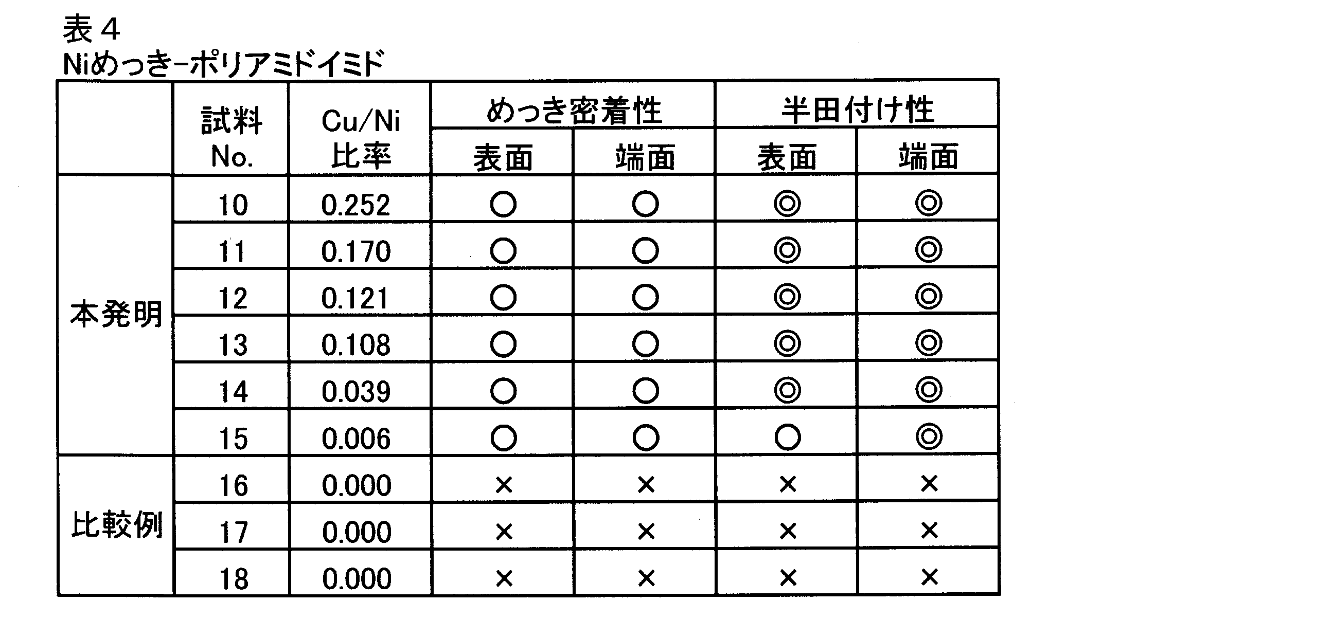
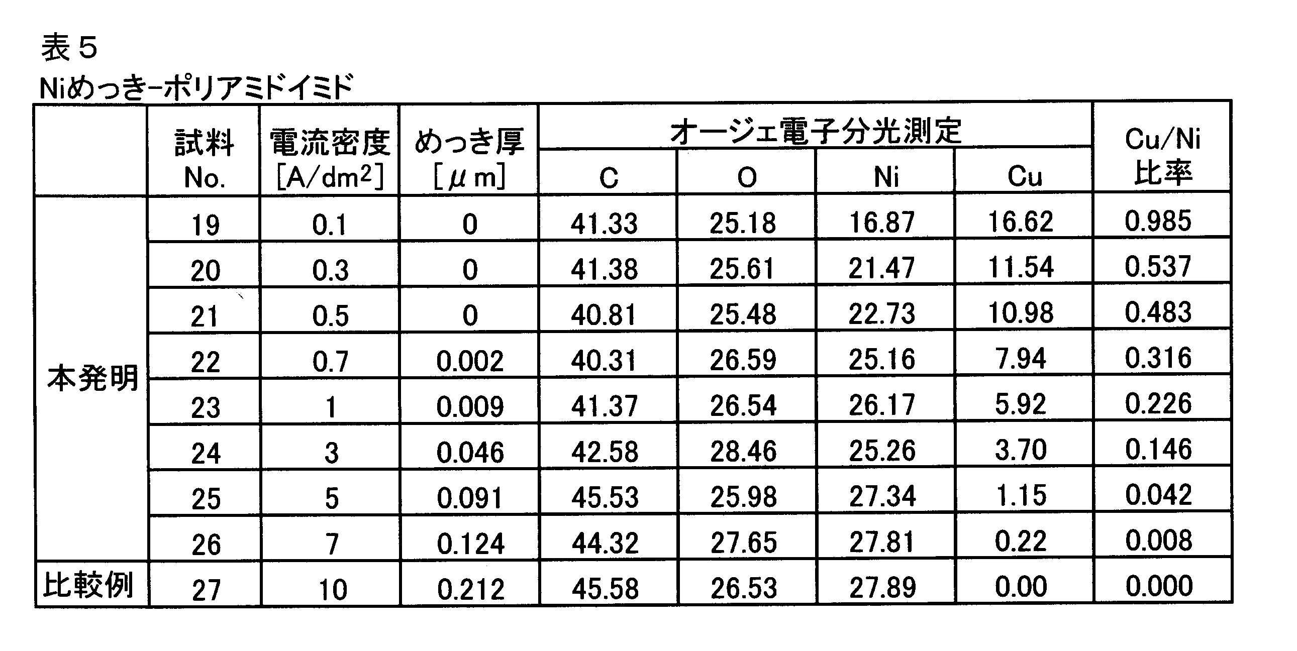
Niめっきが施された金属条に絶縁コーティング層を設ける前に250℃で1時間の熱処理を施した他は、実施例2と同様に、本発明例および比較例の電気電子部品用複合材料を製造し、評価試験を行った。その結果を表5、表6に示す。

Niめっきの代わりにNi-10%Znめっき、Ni-30%Znめっき、Ni-Feめっきを施した他は、実施例1および2と同様に、本発明例および比較例の電気電子部品用複合材料を製造した。
前記Ni-10%Zn合金めっきは、硫酸ニッケル5g/リットル、ピロリン酸亜鉛1g/リットル、ピロリン酸カリウム100g/リットルを含むめっき液中において、液温40℃で電流密度0.5~5A/dm2の条件で行った。
前記Ni-30%Zn合金めっきは、塩化ニッケル75g/リットル、塩化亜鉛30g/リットル、塩化アンモニウム30g/リットル、チオシアン化ナトリウム15g/リットルを含むめっき液中において、液温25℃で電流密度0.05~0.5A/dm2の条件で行った。
前記Ni-Fe合金めっきは、硫酸ニッケル250g/リットル、硫酸鉄50g/リットル、ホウ酸40g/リットルを含むめっき液中において、液温50℃で電流密度1~10A/dm2の条件で行った。
得られた材料に対するめっき密着性および半田付け性の評価結果を表7に示す。

Claims (6)
- 電気電子部品の材料として用いられる、少なくとも表面がCuまたはCu合金である金属基材上の少なくとも一部に絶縁皮膜が設けられた電気電子部品用複合材料であって、前記金属基材と前記絶縁皮膜との間にNiまたはNi合金にCuが拡散された金属層が介在し、前記金属層の最表面をオージェ電子分光測定した際のNiに対するCuの原子数比率(Cu/Ni)が0.005以上であることを特徴とする電気電子部品用複合材料。
- 前記絶縁皮膜がポリイミドまたはポリアミドイミドからなることを特徴とする請求項1に記載の電気電子部品用複合材料。
- 前記金属層は、表面にCuが熱拡散している層であることを特徴とする請求項1または2に記載の電気電子部品用複合材料。
- 請求項1~3のいずれか1項に記載の電気電子部品用複合材料を用いた電気電子部品であって、前記金属層の少なくとも一部にめっき処理が行われて形成されたことを特徴とする電気電子部品。
- 請求項1~3のいずれか1項に記載の電気電子部品用複合材料を用いた電気電子部品であって、前記金属層の少なくとも一部に半田付け処理が行われて形成されたことを特徴とする電気電子部品。
- 少なくとも表面がCuまたはCu合金である金属基材上の少なくとも一部にNiまたはNi合金からなる金属層を介して絶縁皮膜を形成し、前記絶縁皮膜を形成する前または後において熱処理を行い、前記金属層表面にCuを熱拡散させ、前記金属層の最表面をオージェ電子分光測定した際のNiに対するCuの原子数比率(Cu/Ni)を0.005以上とすることを特徴とする電気電子部品用複合材料の製造方法。
Priority Applications (5)
| Application Number | Priority Date | Filing Date | Title |
|---|---|---|---|
| CN2009801226182A CN102066614B (zh) | 2008-06-24 | 2009-06-23 | 电气电子部件用复合材料以及使用其的电气电子部件 |
| EP09770166A EP2295618A4 (en) | 2008-06-24 | 2009-06-23 | COMPOSITE FOR ELECTRICAL / ELECTRONIC COMPONENT AND ELECTRICAL / ELECTRONIC COMPONENT THEREFOR |
| KR1020117001434A KR101370137B1 (ko) | 2008-06-24 | 2009-06-23 | 전기전자 부품용 복합재료 및 그것을 이용한 전기전자 부품 |
| JP2010518028A JP4748550B2 (ja) | 2008-06-24 | 2009-06-23 | 電気電子部品用複合材料およびそれを用いた電気電子部品 |
| US12/977,167 US8337997B2 (en) | 2008-06-24 | 2010-12-23 | Composite material for electrical/electronic part and electrical/electronic part using the same |
Applications Claiming Priority (2)
| Application Number | Priority Date | Filing Date | Title |
|---|---|---|---|
| JP2008164850 | 2008-06-24 | ||
| JP2008-164850 | 2008-06-24 |
Related Child Applications (1)
| Application Number | Title | Priority Date | Filing Date |
|---|---|---|---|
| US12/977,167 Continuation US8337997B2 (en) | 2008-06-24 | 2010-12-23 | Composite material for electrical/electronic part and electrical/electronic part using the same |
Publications (1)
| Publication Number | Publication Date |
|---|---|
| WO2009157456A1 true WO2009157456A1 (ja) | 2009-12-30 |
Family
ID=41444522
Family Applications (1)
| Application Number | Title | Priority Date | Filing Date |
|---|---|---|---|
| PCT/JP2009/061429 Ceased WO2009157456A1 (ja) | 2008-06-24 | 2009-06-23 | 電気電子部品用複合材料およびそれを用いた電気電子部品 |
Country Status (7)
| Country | Link |
|---|---|
| US (1) | US8337997B2 (ja) |
| EP (1) | EP2295618A4 (ja) |
| JP (1) | JP4748550B2 (ja) |
| KR (1) | KR101370137B1 (ja) |
| CN (1) | CN102066614B (ja) |
| TW (1) | TWI449809B (ja) |
| WO (1) | WO2009157456A1 (ja) |
Cited By (1)
| Publication number | Priority date | Publication date | Assignee | Title |
|---|---|---|---|---|
| JP2020179525A (ja) * | 2019-04-23 | 2020-11-05 | 株式会社シミズ | 銅害防止膜、銅害防止膜付き銅部材の製造方法および銅害防止方法 |
Families Citing this family (11)
| Publication number | Priority date | Publication date | Assignee | Title |
|---|---|---|---|---|
| CN102255061A (zh) * | 2011-06-14 | 2011-11-23 | 深圳市豪鹏科技有限公司 | 电池及其所用的绝缘面片 |
| US11268526B2 (en) | 2013-07-09 | 2022-03-08 | Raytheon Technologies Corporation | Plated polymer fan |
| WO2015006421A1 (en) | 2013-07-09 | 2015-01-15 | United Technologies Corporation | Metal-encapsulated polymeric article |
| EP3019723A4 (en) | 2013-07-09 | 2017-05-10 | United Technologies Corporation | Plated polymer compressor |
| WO2015006397A1 (en) * | 2013-07-09 | 2015-01-15 | United Technologies Corporation | Industrial products formed from plated polymers |
| CA2917916A1 (en) | 2013-07-09 | 2015-02-05 | United Technologies Corporation | Plated polymer nosecone |
| JP7524567B2 (ja) * | 2020-03-19 | 2024-07-30 | 三菱マテリアル株式会社 | 絶縁皮膜付き打ち抜き加工品及びその製造方法 |
| RU2769782C1 (ru) * | 2021-10-28 | 2022-04-06 | Федеральное государственное бюджетное образовательное учреждение высшего образования "Сибирский государственный индустриальный университет" ФГБОУ ВО "СибГИУ" | СПОСОБ НАНЕСЕНИЯ ЭЛЕКТРОЭРОЗИОННОСТОЙКИХ ПОКРЫТИЙ СИСТЕМЫ Ni-C-Ag-N НА МЕДНЫЕ ЭЛЕКТРИЧЕСКИЕ КОНТАКТЫ |
| RU2768808C1 (ru) * | 2021-10-28 | 2022-03-24 | Федеральное государственное бюджетное образовательное учреждение высшего образования "Сибирский государственный индустриальный университет" ФГБОУ ВО "СибГИУ" | СПОСОБ НАНЕСЕНИЯ ЭЛЕКТРОЭРОЗИОННОСТОЙКИХ ПОКРЫТИЙ СИСТЕМЫ Mo-C-Ag-N НА МЕДНЫЕ ЭЛЕКТРИЧЕСКИЕ КОНТАКТЫ |
| RU2768806C1 (ru) * | 2021-10-28 | 2022-03-24 | Федеральное государственное бюджетное образовательное учреждение высшего образования "Сибирский государственный индустриальный университет" ФГБОУ ВО "СибГИУ" | Способ нанесения электроэрозионностойких покрытий на основе серебра, кобальта и нитридов кобальта на медные электрические контакты |
| RU210834U1 (ru) * | 2021-12-27 | 2022-05-06 | Федеральное государственное бюджетное образовательное учреждение высшего образования "Сибирский государственный индустриальный университет", ФГБОУ ВО "СибГИУ" | Высоковольтный разъединитель |
Citations (7)
| Publication number | Priority date | Publication date | Assignee | Title |
|---|---|---|---|---|
| JPS6480056A (en) * | 1987-09-21 | 1989-03-24 | Dainippon Printing Co Ltd | Manufacture of conductive material for electronic component |
| JPH051367A (ja) * | 1991-06-24 | 1993-01-08 | Mitsubishi Electric Corp | 電気・電子機器用銅合金材料 |
| JPH05130759A (ja) | 1991-10-31 | 1993-05-25 | Toshiba Corp | 回転電機巻線の絶縁方法 |
| JP2000113731A (ja) * | 1998-10-07 | 2000-04-21 | Mitsui Mining & Smelting Co Ltd | 高導電性・高屈曲性銅合金線 |
| JP2002237542A (ja) | 2001-02-08 | 2002-08-23 | Sumitomo Electric Ind Ltd | 電子部品収納パッケージ用金属キャップ |
| JP2004197224A (ja) | 2002-12-03 | 2004-07-15 | Furukawa Electric Co Ltd:The | 電気電子部品用金属材料 |
| JP2006086513A (ja) * | 2004-08-16 | 2006-03-30 | Furukawa Electric Co Ltd:The | 電気電子部品ケースまたはシールドケースの材料及びその製造方法 |
Family Cites Families (7)
| Publication number | Priority date | Publication date | Assignee | Title |
|---|---|---|---|---|
| JPS5427103B2 (ja) * | 1973-11-12 | 1979-09-07 | ||
| US4019877A (en) * | 1975-10-21 | 1977-04-26 | Westinghouse Electric Corporation | Method for coating of polyimide by electrodeposition |
| US4720401A (en) * | 1985-01-11 | 1988-01-19 | International Business Machines Corporation | Enhanced adhesion between metals and polymers |
| US5246564A (en) * | 1991-10-22 | 1993-09-21 | Sumitomo Metal Mining Company, Limited | Method of manufacturing copper-polyimide substrate |
| US5916695A (en) * | 1995-12-18 | 1999-06-29 | Olin Corporation | Tin coated electrical connector |
| JP4158942B2 (ja) * | 2006-10-03 | 2008-10-01 | 古河電気工業株式会社 | 金属張積層体の製造方法 |
| JP5306641B2 (ja) * | 2006-12-27 | 2013-10-02 | 古河電気工業株式会社 | 電気電子部品用複合材料、電気電子部品および電気電子部品用複合材料の製造方法 |
-
2009
- 2009-06-23 JP JP2010518028A patent/JP4748550B2/ja not_active Expired - Fee Related
- 2009-06-23 WO PCT/JP2009/061429 patent/WO2009157456A1/ja not_active Ceased
- 2009-06-23 CN CN2009801226182A patent/CN102066614B/zh not_active Expired - Fee Related
- 2009-06-23 KR KR1020117001434A patent/KR101370137B1/ko not_active Expired - Fee Related
- 2009-06-23 EP EP09770166A patent/EP2295618A4/en not_active Withdrawn
- 2009-06-24 TW TW098121116A patent/TWI449809B/zh not_active IP Right Cessation
-
2010
- 2010-12-23 US US12/977,167 patent/US8337997B2/en not_active Expired - Fee Related
Patent Citations (7)
| Publication number | Priority date | Publication date | Assignee | Title |
|---|---|---|---|---|
| JPS6480056A (en) * | 1987-09-21 | 1989-03-24 | Dainippon Printing Co Ltd | Manufacture of conductive material for electronic component |
| JPH051367A (ja) * | 1991-06-24 | 1993-01-08 | Mitsubishi Electric Corp | 電気・電子機器用銅合金材料 |
| JPH05130759A (ja) | 1991-10-31 | 1993-05-25 | Toshiba Corp | 回転電機巻線の絶縁方法 |
| JP2000113731A (ja) * | 1998-10-07 | 2000-04-21 | Mitsui Mining & Smelting Co Ltd | 高導電性・高屈曲性銅合金線 |
| JP2002237542A (ja) | 2001-02-08 | 2002-08-23 | Sumitomo Electric Ind Ltd | 電子部品収納パッケージ用金属キャップ |
| JP2004197224A (ja) | 2002-12-03 | 2004-07-15 | Furukawa Electric Co Ltd:The | 電気電子部品用金属材料 |
| JP2006086513A (ja) * | 2004-08-16 | 2006-03-30 | Furukawa Electric Co Ltd:The | 電気電子部品ケースまたはシールドケースの材料及びその製造方法 |
Non-Patent Citations (1)
| Title |
|---|
| See also references of EP2295618A4 |
Cited By (1)
| Publication number | Priority date | Publication date | Assignee | Title |
|---|---|---|---|---|
| JP2020179525A (ja) * | 2019-04-23 | 2020-11-05 | 株式会社シミズ | 銅害防止膜、銅害防止膜付き銅部材の製造方法および銅害防止方法 |
Also Published As
| Publication number | Publication date |
|---|---|
| JP4748550B2 (ja) | 2011-08-17 |
| KR101370137B1 (ko) | 2014-03-05 |
| JPWO2009157456A1 (ja) | 2011-12-15 |
| TWI449809B (zh) | 2014-08-21 |
| CN102066614B (zh) | 2013-07-10 |
| EP2295618A1 (en) | 2011-03-16 |
| TW201005124A (en) | 2010-02-01 |
| US8337997B2 (en) | 2012-12-25 |
| CN102066614A (zh) | 2011-05-18 |
| KR20110029150A (ko) | 2011-03-22 |
| EP2295618A4 (en) | 2011-07-27 |
| US20110091740A1 (en) | 2011-04-21 |
Similar Documents
| Publication | Publication Date | Title |
|---|---|---|
| JP4748550B2 (ja) | 電気電子部品用複合材料およびそれを用いた電気電子部品 | |
| CN101636514B (zh) | 印刷基板端子 | |
| JP4748551B2 (ja) | 電気電子部品用複合材料、その製造方法および電気電子部品 | |
| EP3489385B1 (en) | Electroless palladium/gold plating process | |
| JP4805409B2 (ja) | 電気電子部品用複合材料およびそれを用いた電気電子部品 | |
| JP5185759B2 (ja) | 導電材及びその製造方法 | |
| JP5306641B2 (ja) | 電気電子部品用複合材料、電気電子部品および電気電子部品用複合材料の製造方法 | |
| JP4316652B1 (ja) | 電気電子部品用複合材料、電気電子部品および電気電子部品用複合材料の製造方法 | |
| JP4570948B2 (ja) | ウィスカー発生を抑制したCu−Zn系合金のSnめっき条及びその製造方法 | |
| JP5174733B2 (ja) | メタルコア基板、メタルプレート用導電部材及びこれらの製造方法 | |
| JP2008179888A (ja) | 電気電子部品用複合材料、電気電子部品および電気電子部品用複合材料の製造方法 | |
| JP2006281453A (ja) | 電気電子部品用材料及びその製造方法 | |
| CN101617066A (zh) | 电气电子部件用复合材料、电气电子部件及电气电子部件用复合材料的制造方法 | |
| JP4856745B2 (ja) | フレキシブル基板用導体およびその製造方法並びにフレキシブル基板 | |
| JP2010042572A (ja) | 電気電子部品用複合材料および電気電子部品 |
Legal Events
| Date | Code | Title | Description |
|---|---|---|---|
| WWE | Wipo information: entry into national phase |
Ref document number: 200980122618.2 Country of ref document: CN |
|
| WWE | Wipo information: entry into national phase |
Ref document number: 2010518028 Country of ref document: JP |
|
| 121 | Ep: the epo has been informed by wipo that ep was designated in this application |
Ref document number: 09770166 Country of ref document: EP Kind code of ref document: A1 |
|
| REEP | Request for entry into the european phase |
Ref document number: 2009770166 Country of ref document: EP |
|
| WWE | Wipo information: entry into national phase |
Ref document number: 2009770166 Country of ref document: EP |
|
| NENP | Non-entry into the national phase |
Ref country code: DE |
|
| ENP | Entry into the national phase |
Ref document number: 20117001434 Country of ref document: KR Kind code of ref document: A |