WO2009157462A1 - 光電変換素子の製造方法 - Google Patents
光電変換素子の製造方法 Download PDFInfo
- Publication number
- WO2009157462A1 WO2009157462A1 PCT/JP2009/061450 JP2009061450W WO2009157462A1 WO 2009157462 A1 WO2009157462 A1 WO 2009157462A1 JP 2009061450 W JP2009061450 W JP 2009061450W WO 2009157462 A1 WO2009157462 A1 WO 2009157462A1
- Authority
- WO
- WIPO (PCT)
- Prior art keywords
- dye
- partition member
- partition
- semiconductor electrode
- conversion element
- Prior art date
- Legal status (The legal status is an assumption and is not a legal conclusion. Google has not performed a legal analysis and makes no representation as to the accuracy of the status listed.)
- Ceased
Links
Images
Classifications
-
- H—ELECTRICITY
- H01—ELECTRIC ELEMENTS
- H01M—PROCESSES OR MEANS, e.g. BATTERIES, FOR THE DIRECT CONVERSION OF CHEMICAL ENERGY INTO ELECTRICAL ENERGY
- H01M14/00—Electrochemical current or voltage generators not provided for in groups H01M6/00 - H01M12/00; Manufacture thereof
- H01M14/005—Photoelectrochemical storage cells
-
- H—ELECTRICITY
- H01—ELECTRIC ELEMENTS
- H01G—CAPACITORS; CAPACITORS, RECTIFIERS, DETECTORS, SWITCHING DEVICES, LIGHT-SENSITIVE OR TEMPERATURE-SENSITIVE DEVICES OF THE ELECTROLYTIC TYPE
- H01G9/00—Electrolytic capacitors, rectifiers, detectors, switching devices, light-sensitive or temperature-sensitive devices; Processes of their manufacture
- H01G9/20—Light-sensitive devices
- H01G9/2059—Light-sensitive devices comprising an organic dye as the active light absorbing material, e.g. adsorbed on an electrode or dissolved in solution
- H01G9/2063—Light-sensitive devices comprising an organic dye as the active light absorbing material, e.g. adsorbed on an electrode or dissolved in solution comprising a mixture of two or more dyes
-
- H—ELECTRICITY
- H01—ELECTRIC ELEMENTS
- H01G—CAPACITORS; CAPACITORS, RECTIFIERS, DETECTORS, SWITCHING DEVICES, LIGHT-SENSITIVE OR TEMPERATURE-SENSITIVE DEVICES OF THE ELECTROLYTIC TYPE
- H01G9/00—Electrolytic capacitors, rectifiers, detectors, switching devices, light-sensitive or temperature-sensitive devices; Processes of their manufacture
- H01G9/20—Light-sensitive devices
- H01G9/2068—Panels or arrays of photoelectrochemical cells, e.g. photovoltaic modules based on photoelectrochemical cells
-
- H—ELECTRICITY
- H01—ELECTRIC ELEMENTS
- H01G—CAPACITORS; CAPACITORS, RECTIFIERS, DETECTORS, SWITCHING DEVICES, LIGHT-SENSITIVE OR TEMPERATURE-SENSITIVE DEVICES OF THE ELECTROLYTIC TYPE
- H01G9/00—Electrolytic capacitors, rectifiers, detectors, switching devices, light-sensitive or temperature-sensitive devices; Processes of their manufacture
- H01G9/20—Light-sensitive devices
- H01G9/2068—Panels or arrays of photoelectrochemical cells, e.g. photovoltaic modules based on photoelectrochemical cells
- H01G9/2072—Panels or arrays of photoelectrochemical cells, e.g. photovoltaic modules based on photoelectrochemical cells comprising two or more photoelectrodes sensible to different parts of the solar spectrum, e.g. tandem cells
-
- H—ELECTRICITY
- H01—ELECTRIC ELEMENTS
- H01G—CAPACITORS; CAPACITORS, RECTIFIERS, DETECTORS, SWITCHING DEVICES, LIGHT-SENSITIVE OR TEMPERATURE-SENSITIVE DEVICES OF THE ELECTROLYTIC TYPE
- H01G9/00—Electrolytic capacitors, rectifiers, detectors, switching devices, light-sensitive or temperature-sensitive devices; Processes of their manufacture
- H01G9/20—Light-sensitive devices
- H01G9/2027—Light-sensitive devices comprising an oxide semiconductor electrode
- H01G9/2031—Light-sensitive devices comprising an oxide semiconductor electrode comprising titanium oxide, e.g. TiO2
-
- Y—GENERAL TAGGING OF NEW TECHNOLOGICAL DEVELOPMENTS; GENERAL TAGGING OF CROSS-SECTIONAL TECHNOLOGIES SPANNING OVER SEVERAL SECTIONS OF THE IPC; TECHNICAL SUBJECTS COVERED BY FORMER USPC CROSS-REFERENCE ART COLLECTIONS [XRACs] AND DIGESTS
- Y02—TECHNOLOGIES OR APPLICATIONS FOR MITIGATION OR ADAPTATION AGAINST CLIMATE CHANGE
- Y02E—REDUCTION OF GREENHOUSE GAS [GHG] EMISSIONS, RELATED TO ENERGY GENERATION, TRANSMISSION OR DISTRIBUTION
- Y02E10/00—Energy generation through renewable energy sources
- Y02E10/50—Photovoltaic [PV] energy
- Y02E10/542—Dye sensitized solar cells
-
- Y—GENERAL TAGGING OF NEW TECHNOLOGICAL DEVELOPMENTS; GENERAL TAGGING OF CROSS-SECTIONAL TECHNOLOGIES SPANNING OVER SEVERAL SECTIONS OF THE IPC; TECHNICAL SUBJECTS COVERED BY FORMER USPC CROSS-REFERENCE ART COLLECTIONS [XRACs] AND DIGESTS
- Y02—TECHNOLOGIES OR APPLICATIONS FOR MITIGATION OR ADAPTATION AGAINST CLIMATE CHANGE
- Y02P—CLIMATE CHANGE MITIGATION TECHNOLOGIES IN THE PRODUCTION OR PROCESSING OF GOODS
- Y02P70/00—Climate change mitigation technologies in the production process for final industrial or consumer products
- Y02P70/50—Manufacturing or production processes characterised by the final manufactured product
Definitions
- the present invention relates to a method for manufacturing a photoelectric conversion element, and more particularly, to a method for manufacturing a photoelectric conversion element that allows easy coloring of a dye.
- this dye-sensitized solar cell includes that the manufacturing process is simple and that design can be imparted.
- a solar cell having a plurality of colors can be installed without impairing the appearance of an installed device, a building, or the like, which is considered to lead to further spread of solar cells.
- Applications include, for example, power supplies for various electronic devices such as portable chargers, portable music players, personal computers, electronic cameras, recorders, mobile phones, and watches that have been used with solar cells such as silicon. It can be applied to calculators, as well as window glass and walls, and other signs and signs installed outdoors.
- Patent Document 1 As a method for manufacturing this type of dye-sensitized solar cell.
- the element that determines the color is a dye, and in the manufacturing process, a so-called color separation technique is required in which an arbitrary dye is adsorbed at an arbitrary place on the nanoporous semiconductor electrode. .
- Patent Document 1 since it is difficult to separate the dye when adsorbing the dye to the semiconductor electrode, there is an increasing demand to easily separate the dye. .
- the present invention has been made in view of such circumstances, and in the manufacture of an optical conversion element such as a dye-sensitized solar cell, when the dye is adsorbed to the semiconductor electrode, the dye is simply applied separately. Is to be able to.
- the method for producing a photoelectric conversion element includes a partition member having a partition wall having a predetermined shape on a semiconductor electrode for a photoelectric conversion element, and a different dye solution for each partition partitioned by the partition wall. And adsorbing a predetermined dye, and after a predetermined time has elapsed, removing the semiconductor electrode having the dye adsorbed in a predetermined area corresponding to the section from the partition member.
- the partition member has a container shape having a bottom, and in the step of adsorbing the dye, after the dye solution is put into the section of the partition member, the semiconductor is formed on the opening side of the partition member.
- An electrode is installed to seal the container-shaped partition member, and the partition member sealed in that state is turned upside down to adsorb a dye to a predetermined region on the semiconductor electrode corresponding to the partition.
- the partition member has a hollow shape, and in the step of adsorbing the dye, the partition member is installed on the semiconductor electrode, and the bottom of the partition member is the semiconductor electrode.
- the dye solution is introduced from the opening side of the partition member, and the dye is adsorbed to a predetermined region on the semiconductor electrode corresponding to the partition.
- the partition member includes a first partition member having a first partition and the second partition member having a second partition different from the first partition, and in the step of adsorbing the dye, After the dye is adsorbed to the first region on the semiconductor electrode corresponding to the first partition by the first partition member, the semiconductor corresponding to the second partition by the second partition member The dye is adsorbed in a second region different from the first region on the electrode.
- the semiconductor electrode and the partition member are bonded with an adhesive or pressed with a gasket.
- the internal space is decompressed by a vacuum pump to bond the partition member and the semiconductor electrode.
- the photoelectric conversion element is a dye-sensitized solar cell.
- a partition member having a partition wall having a predetermined shape is installed on a semiconductor electrode for a photoelectric conversion element, and a different dye solution for each partition partitioned by the partition wall After the predetermined amount of dye is adsorbed and a predetermined time has elapsed, the semiconductor electrode having the dye adsorbed in a predetermined region corresponding to the section is peeled off from the partition member.
- the pigments can be easily applied separately.
- a transparent substrate such as conductive glass is laser-processed by laser scribing processing to obtain a patterned transparent substrate.
- a predetermined paste is applied onto the transparent substrate by the screen printing method, and then (3) annealing by heating at 100 ° C. to 600 ° C. in an electric furnace, for example.
- a semiconductor electrode can be obtained by performing for about 1 hour.
- a predetermined dye is adsorbed on the semiconductor electrode, (5) after being bonded to the counter electrode, an antireflection film, etc., (6) (7) A dye-sensitized solar cell is obtained by sealing the liquid injection port.
- a dye-sensitized solar cell is manufactured through the manufacturing process as described above. (4) In the dye adsorption process, when the dye is adsorbed to the semiconductor electrode, the dye is separately applied. What has been difficult is as described above in [Problems to be solved by the invention]. Therefore, in the manufacturing process to which the present invention is applied, a dye adsorption process capable of solving such a problem is performed. Hereinafter, the dye adsorption process will be described with specific examples in [Example 1] to [Example 5].
- a commercially available TiO 2 paste is applied on a commercially available FTO glass (15 ⁇ / ⁇ ) by screen printing, and the temperature is 500 ° C. Is fired for 1 hour to obtain a titanium oxide electrode (average film thickness 20 ⁇ m) having a strip-like pattern.
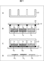
- FIG. 1 is described as (1) to the strip-shaped titanium oxide electrode obtained by the process of (3), the semiconductor electrode 12 1 to 12 3.
- the instrument 21 consists of a container shape (tray shape) with a bottom part. Moreover, the instrument 21 has a partition wall of a predetermined shape, and a different dye solution can be put in each section partitioned by the partition wall.
- the instrument 21 is divided into three compartments, in which three different dye solutions are placed. That is, for example, by dissolving three kinds of dyes N719, Black dye, and D149 in a CH3CN / t-BuOH mixed solution, a 0.3 mM dye solution (dye solutions S 1 , S 2 , S 3 ) is obtained. As such, this dye solution can be poured into each of the three compartments of the device 21 of FIG.
- the transparent substrate 11 is placed on the upper edge (opening upper edge side) of the partition wall of the instrument 21 in which the three different kinds of dye solutions S 1 to S 3 are placed, and the semiconductor electrode
- the appliance 21 is hermetically sealed by installing so that the surface on which 12 1 to 12 3 (titanium oxide electrode) is formed is on the lower side (the appliance 21 side).
- the transparent substrate 11 and the instrument 21 are bonded together and fixed by an adhesive 22 indicated by a black circle in the drawing.
- a bonding method in addition to a method using an adhesive 22 such as a UV curable adhesive, for example, a method of performing pressure bonding using a material that functions as a gasket such as silicon rubber can be used. .
- the silicon rubber may be bonded to the instrument 21 or a sheet-like material may be used.
- the transparent substrate 11 for example, a glass substrate such as conductive glass, a transparent plastic substrate, a metal plate, or the like is used.
- the transparent substrate 11 and the instrument 21 are bonded to each other and the sealed instrument 21 is turned upside down, the state shown in FIG. That is, when the upper and lower sides of the instrument 21 are inverted, the dye solutions S 1 to S 3 existing on the bottom side of the instrument 21 flow into the transparent substrate 11 side, and at the same time, the semiconductor electrodes 12 1 to 12 3 become the dye solution S. It will be filled with 1 to S 3 respectively. As a result, the dye is adsorbed to each of the semiconductor electrodes 12 1 to 12 3 .
- the semiconductor electrode 12 1 has the dye adsorbed by the dye solution S 1
- the semiconductor electrode 12 2 has the dye adsorbed by the dye solution S 2
- the semiconductor electrode 12 3 has the dye adsorbed by the dye solution S 3 .
- an arbitrary dye is adsorbed at an arbitrary position on the semiconductor electrode, and further, the dye can be separately applied only by preparing the instrument 21, which is convenient. I can say that.
- the height of the partition wall is required to be at least 3 mm. This is because if the amount is less than that, the amount of the dye contained in the dye solution poured into the semiconductor electrode 12 becomes insufficient.
- the upper limit of the partition wall height is not particularly limited to 3 mm or more.
- the width of the partition wall is not particularly limited, but in practice it is preferably 10 mm or less. If it is more than that, the area contributing to power generation in the area of the solar cell is reduced, so it is not at a level that can withstand practical use.
- a dye-sensitized solar cell is obtained by laminating using a counter electrode and a UV curable adhesive and injecting an electrolytic solution therein. Accordingly, a dye-sensitized solar cell in which a predetermined dye is adsorbed at a predetermined position is thereby obtained.
- the density can be controlled by changing the adsorption time, the concentration of the dye solution, the type of solvent, and the like for each unit.
- a dye representing letters, numbers, symbols, figures, or any combination thereof can be adsorbed on the semiconductor electrode. The same applies to other embodiments described later.
- Example 1 as an example of the bonding method of the appliance 21, in addition to the example of using the adhesive 22, an example of crimping with a gasket has been described. It is also possible to employ a technique of pressure bonding using atmospheric pressure, such as bonding in a vacuum and returning to the atmosphere.
- an instrument 21 having a partition wall into which three kinds of dye solutions S 1 to S 3 similar to those in [Example 1] are injected and provided with a silicon rubber layer on its outer periphery is shown in [Example 1].
- [Example 1] are mechanically bonded to the semiconductor electrodes 12 1 to 12 3 manufactured by the same method (steps (1) to (3)). Thereafter, the internal space of the instrument 21 that has been sealed by being bonded together is sufficiently adhered by reducing the pressure using a vacuum pump, and this is moved up and down in the same manner as in [Example 1]. After inversion, it was allowed to stand for 24 hours.
- the semiconductor electrodes 12 1 to 12 3 that are inverted and located below the instrument 21 are returned to the upper side again, and the interior is returned to atmospheric pressure, and the transparent substrate 11 is peeled off.
- Semiconductor electrodes 12 1 to 12 3 are obtained separately.
- this dye-attached semiconductor electrode was bonded using a platinum sputter counter electrode and a UV curable adhesive in the same manner as in [Example 1] (steps (5), (6), (7)), and an electrolytic solution. By injecting, a dye-sensitized solar cell can be obtained.
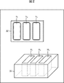
- Example 1 by inverting the top and bottom of the instrument 21 Fig. 1 has been described for the case where the adsorption of the dye to the semiconductor electrode 12 1 to 12 3, by using the jig 31 of FIG. 2 The dye can be adsorbed without inverting the member.
- the lower diagram shows a perspective view of the jig 31, and the upper diagram shows a top view of the silicon rubber 32.
- a hollow jig 31 is used. It is mechanically pressure-bonded through a silicon rubber 32 having holes h 1 to h 3 having shapes corresponding to the portions H 1 to H 3 . That is, at this time, the semiconductor electrodes 12 1 to 12 3 are positioned at the bottom of the jig 31 having a hollow shape. Thereafter, three types of dye solutions S 1 to S 3 similar to those in [Example 1] are injected into the three hollow portions H 1 to H 3 provided in the jig 31, respectively. The dye is adsorbed to the semiconductor electrodes 12 1 to 12 3 which are pressure-bonded through the silicon rubber 32 as the bottom.
- the semiconductor electrodes 12 1 to 12 3 are separately coated with three kinds of dyes corresponding to the hollow shape of the jig 31 by leaving it as it is for 24 hours. Then, in the same manner as in [Example 1] (steps (5), (6), (7)), this dye-attached semiconductor electrode is bonded using a platinum sputter counter electrode and a UV curable adhesive, and an electrolytic solution is obtained. By injecting, a dye-sensitized solar cell can be obtained.
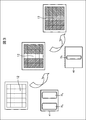
- FIG. 3 shows a top view of the jig 41, the jig 42, and the semiconductor electrode 12. As shown by the arrows in the figure, the semiconductor electrode 12 is arranged from the upper left in the figure to the lower right in the figure. It is lined up in time series in the direction toward Therefore, in FIG. 3, the states of the three semiconductor electrodes 12 arranged in time series from the upper left in the drawing to the lower right in the drawing are referred to as state 1, state 2, and state 3, respectively, from the upper left in the drawing. I will explain.
- a jig 41 having the shape of pattern 1 (hole H 4 and hole H 5 in FIG. 3) and pattern 2 different from pattern 1 (hole H 6 in FIG. 3).
- the jig 41 is installed on the semiconductor electrode 12 in the state 1.
- the holes H 4 and H 5 provided in the jig 41 correspond to the holes H 4 and H 5 .
- Dye solutions S 1 and S 2 are respectively injected into the first and second rows of cells in the figure and the fourth and fifth rows of cells from the left in the figure. More specifically, after the jig 41 is bonded to the semiconductor electrode 12, the dye solutions S 1 and S 2 of N719 and Black dye are respectively injected into the hole H 4 and the hole H 5 and left as they are for 24 hours. By standing still, the semiconductor electrode 12 is adsorbed with the dye having a shape corresponding to the hole H 4 and the hole H 5 of the jig 41.
- the dye solutions S 1 to squares first and second columns dye is adsorbed (in shaded downward right in the drawing
- the dye is adsorbed by the dye solution S 2 in the fourth and fifth rows (the area on the square indicated by the slanting diagonal lines in the figure).
- the middle cell in the third row is in a state where the dye is not adsorbed.
- a predetermined dye is adsorbed on the remaining third row of the semiconductor electrodes 12 by using the jig 42.
- a predetermined dye is adsorbed on the remaining third row of the semiconductor electrodes 12 by using the jig 42.
- rinsed with acetonitrile, by bonding jig 42 in the semiconductor electrode 12 was injected dye solution S 3 of D149 into the hole H 6, by standing still for 24 hours as it is, A dye having a shape corresponding to the hole H 6 of the jig 42 is adsorbed on the semiconductor electrode 12.
- the semiconductor electrode 12 coated with three types of pigments is obtained by coating the pigments in two stages using the jig 41 and the jig 42.
- this dye-attached semiconductor electrode was bonded using a platinum sputter counter electrode and a UV curable adhesive in the same manner as in [Example 1] (steps (5), (6), (7)), and an electrolytic solution. By injecting, a dye-sensitized solar cell can be obtained.
- the titanium oxide electrode may be manufactured by other methods.
- steps (1) to (3) which are the previous steps of the dye adsorption treatment, commercially available titanium oxide P25 is dispersed in 20 wt% with respect to gamma butyrolactone, and further 30 wt% with respect to titanium oxide.
- a PVDF-HFP (polyfucavinylidene-hexafluoropropylene) copolymer is added and stirred while heating to about 60 ° C. to obtain a uniform solution.
- This is coated on a PEN substrate with ITO by a blade coating method, dried at 120 ° C for 1 hour, and then pressed using a roll press to oxidize 5cm x 5cm on the PEN substrate.
- a titanium electrode is obtained.
- a dye-sensitized solar cell can be obtained by processing according to the method (steps (5), (6), (7)). That is, in [Embodiment 5], since the titanium oxide electrode is formed on a flexible substrate such as a PEN substrate, a dye-sensitized solar cell with higher flexibility can be manufactured.
- the dye when an optical conversion element such as a dye-sensitized solar cell is manufactured, the dye can be easily applied when the dye is adsorbed to the semiconductor electrode.
- the embodiment of the present invention is not limited to the above-described embodiment, and various modifications can be made without departing from the gist of the present invention.
- the numerical values, structures, shapes, materials, raw materials, processes, etc. given in this embodiment are merely examples, and different numerical values, structures, shapes, materials, raw materials, processes are used as necessary. May be.
- a dye-sensitized solar cell has been described as an example of a photoelectric conversion element.
- the present invention is not limited to a dye-sensitized solar cell or a photoelectric conversion element other than a solar cell. Is also applicable.
Landscapes
- Engineering & Computer Science (AREA)
- Power Engineering (AREA)
- Chemical & Material Sciences (AREA)
- Chemical Kinetics & Catalysis (AREA)
- Electrochemistry (AREA)
- Microelectronics & Electronic Packaging (AREA)
- Life Sciences & Earth Sciences (AREA)
- Sustainable Development (AREA)
- Materials Engineering (AREA)
- General Chemical & Material Sciences (AREA)
- Hybrid Cells (AREA)
- Photovoltaic Devices (AREA)
Abstract
Description
(2)スクリーン印刷処理
(3)アニール処理
(4)色素吸着処理
(5)貼り合せ処理
(6)電解液注液処理
(7)注液口の封止処理
Claims (7)
- 光電変換素子用の半導体電極上に、所定の形状からなる隔壁を有する仕切部材を設置し、前記隔壁により仕切られた区画ごとに異なる色素溶液を入れて所定の色素を吸着させる工程と、
所定の時間が経過した後、前記区画に対応する所定の領域に前記色素が吸着された前記半導体電極を前記仕切部材からはがす工程と
を備える光電変換素子の製造方法。 - 前記仕切部材は、底部を持つ容器型の形状を有しており、
前記色素を吸着させる工程において、前記仕切部材の前記区画に前記色素溶液を入れた後、前記仕切部材の開口側に前記半導体電極を設置して容器型の前記仕切部材を密閉し、その状態で密閉された前記仕切部材の上下を反転させて、前記区画に対応する前記半導体電極上の所定の領域に色素を吸着させる
請求項1に記載の光電変換素子の製造方法。 - 前記仕切部材は、中空の形状を有しており、
前記色素を吸着させる工程において、前記仕切部材を前記半導体電極上に設置し、前記仕切部材の底部が前記半導体電極となっている状態で、前記仕切部材の開口側から前記色素溶液を入れて、前記区画に対応する前記半導体電極上の所定の領域に色素を吸着させる 請求項1に記載の光電変換素子の製造方法。 - 前記仕切部材は、第1の区画を有する第1の仕切部材と、前記第1の区画とは異なる第2の区画を有する前記第2の仕切部材からなり、
前記色素を吸着させる工程において、前記第1の仕切部材によって、前記第1の区画に対応する前記半導体電極上の第1の領域に色素を吸着させた後、前記第2の仕切部材によって、前記第2の区画に対応する前記半導体電極上の前記第1の領域とは異なる第2の領域に色素を吸着させる
請求項1に記載の光電変換素子の製造方法。 - 前記半導体電極と前記仕切部材とは、接着剤により接着されるか、あるいはガスケットにより圧着される
請求項1に記載の光電変換素子の製造方法。 - 前記仕切部材が密閉された状態で、その内部空間を真空ポンプにより減圧させることによって、前記仕切部材と前記半導体電極とを接着させる
請求項2に記載の光電変換素子の製造方法。 - 前記光電変換素子は、色素増感型太陽電池である
請求項1に記載の光電変換素子の製造方法。
Priority Applications (4)
| Application Number | Priority Date | Filing Date | Title |
|---|---|---|---|
| BRPI0904321-7A BRPI0904321A2 (pt) | 2008-06-24 | 2009-06-24 | Método para fabricar um dispositivo de conversão fotoelétrico |
| CN200980100176A CN101785138A (zh) | 2008-06-24 | 2009-06-24 | 制造光电转换设备的方法 |
| EP09770172A EP2306584A4 (en) | 2008-06-24 | 2009-06-24 | PROCESS FOR PREPARING A PHOTOELECTRIC CONVERSION ELEMENT |
| US12/733,093 US20100144083A1 (en) | 2008-06-24 | 2009-06-24 | Method of manufacturing photoelectric conversion device |
Applications Claiming Priority (2)
| Application Number | Priority Date | Filing Date | Title |
|---|---|---|---|
| JP2008164448A JP2010009769A (ja) | 2008-06-24 | 2008-06-24 | 光電変換素子の製造方法 |
| JP2008-164448 | 2008-06-24 |
Publications (1)
| Publication Number | Publication Date |
|---|---|
| WO2009157462A1 true WO2009157462A1 (ja) | 2009-12-30 |
Family
ID=41444526
Family Applications (1)
| Application Number | Title | Priority Date | Filing Date |
|---|---|---|---|
| PCT/JP2009/061450 Ceased WO2009157462A1 (ja) | 2008-06-24 | 2009-06-24 | 光電変換素子の製造方法 |
Country Status (7)
| Country | Link |
|---|---|
| US (1) | US20100144083A1 (ja) |
| EP (1) | EP2306584A4 (ja) |
| JP (1) | JP2010009769A (ja) |
| KR (1) | KR20110026405A (ja) |
| CN (1) | CN101785138A (ja) |
| BR (1) | BRPI0904321A2 (ja) |
| WO (1) | WO2009157462A1 (ja) |
Cited By (3)
| Publication number | Priority date | Publication date | Assignee | Title |
|---|---|---|---|---|
| CN102315311A (zh) * | 2010-07-06 | 2012-01-11 | 杜邦太阳能有限公司 | 太阳能模块装置及其封边涂布方法 |
| KR101112058B1 (ko) * | 2010-12-31 | 2012-02-24 | 한국생산기술연구원 | 원자층 형성 공정의 선택적 증착으로 투명전극이 제조된 채널 구조의 태양전지 제조방법 |
| JP2012069491A (ja) * | 2010-09-27 | 2012-04-05 | Sekisui Chem Co Ltd | 太陽電池モジュールおよび太陽電池モジュールの製造方法 |
Families Citing this family (16)
| Publication number | Priority date | Publication date | Assignee | Title |
|---|---|---|---|---|
| JP5007784B2 (ja) * | 2006-01-30 | 2012-08-22 | ソニー株式会社 | 光電変換装置 |
| JP2007234580A (ja) * | 2006-02-02 | 2007-09-13 | Sony Corp | 色素増感型光電変換装置 |
| JP2007280906A (ja) * | 2006-04-12 | 2007-10-25 | Sony Corp | 機能デバイス及びその製造方法 |
| JP5023866B2 (ja) * | 2007-07-27 | 2012-09-12 | ソニー株式会社 | 色素増感光電変換素子およびその製造方法ならびに電子機器 |
| JP2009099476A (ja) * | 2007-10-19 | 2009-05-07 | Sony Corp | 色素増感光電変換素子およびその製造方法 |
| JP2009146625A (ja) * | 2007-12-12 | 2009-07-02 | Sony Corp | 色素増感光電変換素子モジュールおよびその製造方法ならびに光電変換素子モジュールおよびその製造方法ならびに電子機器 |
| JP2010003468A (ja) * | 2008-06-19 | 2010-01-07 | Sony Corp | 色素増感太陽電池およびその製造方法 |
| JP2010010191A (ja) * | 2008-06-24 | 2010-01-14 | Sony Corp | 電子装置 |
| JP2010092762A (ja) * | 2008-10-09 | 2010-04-22 | Sony Corp | 機能性デバイス及びその製造方法 |
| US20110048525A1 (en) * | 2008-11-26 | 2011-03-03 | Sony Corporation | Functional device and method for producing the same |
| JP5428555B2 (ja) * | 2009-06-08 | 2014-02-26 | ソニー株式会社 | 色素増感光電変換素子の製造方法 |
| JP2011204662A (ja) * | 2010-03-05 | 2011-10-13 | Sony Corp | 光電変換素子およびその製造方法ならびに電子機器 |
| JP5621488B2 (ja) * | 2010-03-17 | 2014-11-12 | ソニー株式会社 | 光電変換装置 |
| US20140102526A1 (en) * | 2011-06-24 | 2014-04-17 | Sony Corporation | Photoelectric conversion device, method for manufacturing same, dye adsorption device, liquid retaining jig used for dye adsorption device, and method for manufacturing photoelectric conversion element |
| JP2014013716A (ja) * | 2012-07-05 | 2014-01-23 | Nissha Printing Co Ltd | 色素増感型太陽電池、及びその製造方法 |
| JP5969844B2 (ja) * | 2012-07-18 | 2016-08-17 | 株式会社フジクラ | 色素増感太陽電池およびその製造方法 |
Citations (3)
| Publication number | Priority date | Publication date | Assignee | Title |
|---|---|---|---|---|
| JP2000268891A (ja) * | 1999-03-19 | 2000-09-29 | Toshiba Corp | 多色色素増感透明半導体電極部材とその製造方法、多色色素増感型太陽電池、及び表示素子 |
| JP2002299678A (ja) * | 2001-03-29 | 2002-10-11 | Fuji Photo Film Co Ltd | 高感度受光素子及び光センサー |
| JP2005259548A (ja) | 2004-03-12 | 2005-09-22 | Sony Corp | 光電変換素子及びその製造方法 |
Family Cites Families (25)
| Publication number | Priority date | Publication date | Assignee | Title |
|---|---|---|---|---|
| JP4010170B2 (ja) * | 2002-04-11 | 2007-11-21 | ソニー株式会社 | 光電変換素子の製造方法 |
| JP4221643B2 (ja) * | 2002-05-27 | 2009-02-12 | ソニー株式会社 | 光電変換装置 |
| JP4635473B2 (ja) * | 2004-05-13 | 2011-02-23 | ソニー株式会社 | 光電変換素子の製造方法及び半導体電極の製造方法 |
| JP4635474B2 (ja) * | 2004-05-14 | 2011-02-23 | ソニー株式会社 | 光電変換素子、及びこれに用いる透明導電性基板 |
| GB2432718A (en) * | 2005-11-25 | 2007-05-30 | Seiko Epson Corp | Multicolour metal oxide electrochemical cell |
| GB2432966A (en) * | 2005-11-25 | 2007-06-06 | Seiko Epson Corp | Dye-sensitised electrochemical cell |
| JP5007784B2 (ja) * | 2006-01-30 | 2012-08-22 | ソニー株式会社 | 光電変換装置 |
| JP2007234580A (ja) * | 2006-02-02 | 2007-09-13 | Sony Corp | 色素増感型光電変換装置 |
| JP2007280906A (ja) * | 2006-04-12 | 2007-10-25 | Sony Corp | 機能デバイス及びその製造方法 |
| JP5023866B2 (ja) * | 2007-07-27 | 2012-09-12 | ソニー株式会社 | 色素増感光電変換素子およびその製造方法ならびに電子機器 |
| KR100927660B1 (ko) * | 2007-10-16 | 2009-11-20 | 한국전자통신연구원 | 염료 감응 태양 전지 및 그 제조 방법 |
| JP2009099476A (ja) * | 2007-10-19 | 2009-05-07 | Sony Corp | 色素増感光電変換素子およびその製造方法 |
| JP2009110796A (ja) * | 2007-10-30 | 2009-05-21 | Sony Corp | 色素増感光電変換素子モジュールおよびその製造方法ならびに電子機器 |
| JP2009146625A (ja) * | 2007-12-12 | 2009-07-02 | Sony Corp | 色素増感光電変換素子モジュールおよびその製造方法ならびに光電変換素子モジュールおよびその製造方法ならびに電子機器 |
| JP2010003468A (ja) * | 2008-06-19 | 2010-01-07 | Sony Corp | 色素増感太陽電池およびその製造方法 |
| JP2010010191A (ja) * | 2008-06-24 | 2010-01-14 | Sony Corp | 電子装置 |
| JP2010092762A (ja) * | 2008-10-09 | 2010-04-22 | Sony Corp | 機能性デバイス及びその製造方法 |
| US20110048525A1 (en) * | 2008-11-26 | 2011-03-03 | Sony Corporation | Functional device and method for producing the same |
| JP5428555B2 (ja) * | 2009-06-08 | 2014-02-26 | ソニー株式会社 | 色素増感光電変換素子の製造方法 |
| JP2011204662A (ja) * | 2010-03-05 | 2011-10-13 | Sony Corp | 光電変換素子およびその製造方法ならびに電子機器 |
| JP5621488B2 (ja) * | 2010-03-17 | 2014-11-12 | ソニー株式会社 | 光電変換装置 |
| JP2011216190A (ja) * | 2010-03-31 | 2011-10-27 | Sony Corp | 光電変換装置及びその製造方法 |
| JP2011216189A (ja) * | 2010-03-31 | 2011-10-27 | Sony Corp | 光電変換装置及び光電変換装置モジュール |
| JP2011238472A (ja) * | 2010-05-11 | 2011-11-24 | Sony Corp | 光電変換装置 |
| JP2012014849A (ja) * | 2010-06-29 | 2012-01-19 | Sony Corp | 光電変換素子およびその製造方法ならびに光電変換素子モジュールおよびその製造方法 |
-
2008
- 2008-06-24 JP JP2008164448A patent/JP2010009769A/ja not_active Abandoned
-
2009
- 2009-06-24 BR BRPI0904321-7A patent/BRPI0904321A2/pt not_active IP Right Cessation
- 2009-06-24 US US12/733,093 patent/US20100144083A1/en not_active Abandoned
- 2009-06-24 CN CN200980100176A patent/CN101785138A/zh active Pending
- 2009-06-24 WO PCT/JP2009/061450 patent/WO2009157462A1/ja not_active Ceased
- 2009-06-24 KR KR1020107003360A patent/KR20110026405A/ko not_active Withdrawn
- 2009-06-24 EP EP09770172A patent/EP2306584A4/en not_active Withdrawn
Patent Citations (3)
| Publication number | Priority date | Publication date | Assignee | Title |
|---|---|---|---|---|
| JP2000268891A (ja) * | 1999-03-19 | 2000-09-29 | Toshiba Corp | 多色色素増感透明半導体電極部材とその製造方法、多色色素増感型太陽電池、及び表示素子 |
| JP2002299678A (ja) * | 2001-03-29 | 2002-10-11 | Fuji Photo Film Co Ltd | 高感度受光素子及び光センサー |
| JP2005259548A (ja) | 2004-03-12 | 2005-09-22 | Sony Corp | 光電変換素子及びその製造方法 |
Non-Patent Citations (1)
| Title |
|---|
| See also references of EP2306584A4 |
Cited By (3)
| Publication number | Priority date | Publication date | Assignee | Title |
|---|---|---|---|---|
| CN102315311A (zh) * | 2010-07-06 | 2012-01-11 | 杜邦太阳能有限公司 | 太阳能模块装置及其封边涂布方法 |
| JP2012069491A (ja) * | 2010-09-27 | 2012-04-05 | Sekisui Chem Co Ltd | 太陽電池モジュールおよび太陽電池モジュールの製造方法 |
| KR101112058B1 (ko) * | 2010-12-31 | 2012-02-24 | 한국생산기술연구원 | 원자층 형성 공정의 선택적 증착으로 투명전극이 제조된 채널 구조의 태양전지 제조방법 |
Also Published As
| Publication number | Publication date |
|---|---|
| BRPI0904321A2 (pt) | 2015-06-30 |
| KR20110026405A (ko) | 2011-03-15 |
| CN101785138A (zh) | 2010-07-21 |
| US20100144083A1 (en) | 2010-06-10 |
| JP2010009769A (ja) | 2010-01-14 |
| EP2306584A4 (en) | 2012-04-25 |
| EP2306584A1 (en) | 2011-04-06 |
Similar Documents
| Publication | Publication Date | Title |
|---|---|---|
| JP2010009769A (ja) | 光電変換素子の製造方法 | |
| WO2009157461A1 (ja) | 電子装置 | |
| AU2008299574B2 (en) | A method for manufacturing solar cells | |
| JP4640322B2 (ja) | 光電変換素子及びその製造方法、並びに電気化学セルの製造方法 | |
| CN103760730B (zh) | 一种黑矩阵及其制造方法、显示面板及显示装置 | |
| KR20110026404A (ko) | 색소 증감 태양 전지 및 그 제조 방법 | |
| EP3076227B1 (en) | Transmittance-variable film and method for producing same | |
| CN104317129A (zh) | 高通量筛选电致变色材料的电致变色器件及其制备方法 | |
| JP2009032614A (ja) | 色素増感型太陽電池の製造方法及び色素増感型太陽電池 | |
| JP5397585B2 (ja) | 色素増感太陽電池および隔壁形成方法 | |
| JP2014165064A (ja) | 色素増感太陽電池およびその製造方法、および電子機器 | |
| WO2013114995A1 (ja) | 色素増感太陽電池のための電極の製造方法 | |
| KR101446910B1 (ko) | 도전성 유리의 투명전도 산화막 패턴 형성방법 및 이에의하여 제조되는 도전성 유리 | |
| JP2014165049A (ja) | 色素増感太陽電池およびその製造方法、および電子機器 | |
| JP2006179380A (ja) | 意匠性を備えた太陽電池モジュールおよびその製造方法 | |
| KR101642894B1 (ko) | 매립형 전기 변색 소자 및 그 제조 방법 | |
| CN115938315B (zh) | 一种电润湿显示器件及其制备方法与应用 | |
| CN107768525A (zh) | 光伏电池光电转换复合层结构制作方法 | |
| JP4376707B2 (ja) | 透明太陽電池モジュール及びその製造方法 | |
| JP5400737B2 (ja) | 太陽電池モジュールおよび太陽電池モジュールの製造方法 | |
| JP2008181003A5 (ja) | ||
| KR20030067021A (ko) | 전기변색물질을 이용한 패시브 매트릭스 표시장치 및 그제조방법 | |
| KR20120122653A (ko) | 염료 감응 방식 태양전지 및 이의 제조방법 | |
| KR101592716B1 (ko) | 차량 루프용 태양전지 제조방법 | |
| KR20140004837A (ko) | 염료감응 태양전지 제조를 위한 합착 장치 및 그의 합착 플레이트 |
Legal Events
| Date | Code | Title | Description |
|---|---|---|---|
| WWE | Wipo information: entry into national phase |
Ref document number: 200980100176.1 Country of ref document: CN |
|
| WWE | Wipo information: entry into national phase |
Ref document number: 2009770172 Country of ref document: EP |
|
| WWE | Wipo information: entry into national phase |
Ref document number: 12733093 Country of ref document: US |
|
| WWE | Wipo information: entry into national phase |
Ref document number: 940/DELNP/2010 Country of ref document: IN |
|
| ENP | Entry into the national phase |
Ref document number: 20107003360 Country of ref document: KR Kind code of ref document: A |
|
| 121 | Ep: the epo has been informed by wipo that ep was designated in this application |
Ref document number: 09770172 Country of ref document: EP Kind code of ref document: A1 |
|
| NENP | Non-entry into the national phase |
Ref country code: DE |
|
| ENP | Entry into the national phase |
Ref document number: PI0904321 Country of ref document: BR Kind code of ref document: A2 Effective date: 20100217 |