WO2010004792A1 - 液晶表示装置 - Google Patents
液晶表示装置 Download PDFInfo
- Publication number
- WO2010004792A1 WO2010004792A1 PCT/JP2009/057088 JP2009057088W WO2010004792A1 WO 2010004792 A1 WO2010004792 A1 WO 2010004792A1 JP 2009057088 W JP2009057088 W JP 2009057088W WO 2010004792 A1 WO2010004792 A1 WO 2010004792A1
- Authority
- WO
- WIPO (PCT)
- Prior art keywords
- liquid crystal
- crystal display
- substrate
- display device
- substrate surface
- Prior art date
- Legal status (The legal status is an assumption and is not a legal conclusion. Google has not performed a legal analysis and makes no representation as to the accuracy of the status listed.)
- Ceased
Links
Images


Classifications
-
- G—PHYSICS
- G02—OPTICS
- G02B—OPTICAL ELEMENTS, SYSTEMS OR APPARATUS
- G02B6/00—Light guides; Structural details of arrangements comprising light guides and other optical elements, e.g. couplings
- G02B6/0001—Light guides; Structural details of arrangements comprising light guides and other optical elements, e.g. couplings specially adapted for lighting devices or systems
- G02B6/0011—Light guides; Structural details of arrangements comprising light guides and other optical elements, e.g. couplings specially adapted for lighting devices or systems the light guides being planar or of plate-like form
- G02B6/0081—Mechanical or electrical aspects of the light guide and light source in the lighting device peculiar to the adaptation to planar light guides, e.g. concerning packaging
- G02B6/0083—Details of electrical connections of light sources to drivers, circuit boards, or the like
-
- G—PHYSICS
- G02—OPTICS
- G02B—OPTICAL ELEMENTS, SYSTEMS OR APPARATUS
- G02B6/00—Light guides; Structural details of arrangements comprising light guides and other optical elements, e.g. couplings
- G02B6/0001—Light guides; Structural details of arrangements comprising light guides and other optical elements, e.g. couplings specially adapted for lighting devices or systems
- G02B6/0011—Light guides; Structural details of arrangements comprising light guides and other optical elements, e.g. couplings specially adapted for lighting devices or systems the light guides being planar or of plate-like form
- G02B6/0081—Mechanical or electrical aspects of the light guide and light source in the lighting device peculiar to the adaptation to planar light guides, e.g. concerning packaging
- G02B6/0086—Positioning aspects
- G02B6/009—Positioning aspects of the light source in the package
-
- G—PHYSICS
- G02—OPTICS
- G02F—OPTICAL DEVICES OR ARRANGEMENTS FOR THE CONTROL OF LIGHT BY MODIFICATION OF THE OPTICAL PROPERTIES OF THE MEDIA OF THE ELEMENTS INVOLVED THEREIN; NON-LINEAR OPTICS; FREQUENCY-CHANGING OF LIGHT; OPTICAL LOGIC ELEMENTS; OPTICAL ANALOGUE/DIGITAL CONVERTERS
- G02F1/00—Devices or arrangements for the control of the intensity, colour, phase, polarisation or direction of light arriving from an independent light source, e.g. switching, gating or modulating; Non-linear optics
- G02F1/01—Devices or arrangements for the control of the intensity, colour, phase, polarisation or direction of light arriving from an independent light source, e.g. switching, gating or modulating; Non-linear optics for the control of the intensity, phase, polarisation or colour
- G02F1/13—Devices or arrangements for the control of the intensity, colour, phase, polarisation or direction of light arriving from an independent light source, e.g. switching, gating or modulating; Non-linear optics for the control of the intensity, phase, polarisation or colour based on liquid crystals, e.g. single liquid crystal display cells
- G02F1/133—Constructional arrangements; Operation of liquid crystal cells; Circuit arrangements
- G02F1/1333—Constructional arrangements; Manufacturing methods
- G02F1/1335—Structural association of cells with optical devices, e.g. polarisers or reflectors
- G02F1/1336—Illuminating devices
- G02F1/133615—Edge-illuminating devices, i.e. illuminating from the side
-
- G—PHYSICS
- G02—OPTICS
- G02B—OPTICAL ELEMENTS, SYSTEMS OR APPARATUS
- G02B6/00—Light guides; Structural details of arrangements comprising light guides and other optical elements, e.g. couplings
- G02B6/0001—Light guides; Structural details of arrangements comprising light guides and other optical elements, e.g. couplings specially adapted for lighting devices or systems
- G02B6/0011—Light guides; Structural details of arrangements comprising light guides and other optical elements, e.g. couplings specially adapted for lighting devices or systems the light guides being planar or of plate-like form
- G02B6/0013—Means for improving the coupling-in of light from the light source into the light guide
- G02B6/0015—Means for improving the coupling-in of light from the light source into the light guide provided on the surface of the light guide or in the bulk of it
- G02B6/002—Means for improving the coupling-in of light from the light source into the light guide provided on the surface of the light guide or in the bulk of it by shaping at least a portion of the light guide, e.g. with collimating, focussing or diverging surfaces
-
- G—PHYSICS
- G02—OPTICS
- G02B—OPTICAL ELEMENTS, SYSTEMS OR APPARATUS
- G02B6/00—Light guides; Structural details of arrangements comprising light guides and other optical elements, e.g. couplings
- G02B6/0001—Light guides; Structural details of arrangements comprising light guides and other optical elements, e.g. couplings specially adapted for lighting devices or systems
- G02B6/0011—Light guides; Structural details of arrangements comprising light guides and other optical elements, e.g. couplings specially adapted for lighting devices or systems the light guides being planar or of plate-like form
- G02B6/0066—Light guides; Structural details of arrangements comprising light guides and other optical elements, e.g. couplings specially adapted for lighting devices or systems the light guides being planar or of plate-like form characterised by the light source being coupled to the light guide
- G02B6/0073—Light emitting diode [LED]
-
- G—PHYSICS
- G02—OPTICS
- G02F—OPTICAL DEVICES OR ARRANGEMENTS FOR THE CONTROL OF LIGHT BY MODIFICATION OF THE OPTICAL PROPERTIES OF THE MEDIA OF THE ELEMENTS INVOLVED THEREIN; NON-LINEAR OPTICS; FREQUENCY-CHANGING OF LIGHT; OPTICAL LOGIC ELEMENTS; OPTICAL ANALOGUE/DIGITAL CONVERTERS
- G02F1/00—Devices or arrangements for the control of the intensity, colour, phase, polarisation or direction of light arriving from an independent light source, e.g. switching, gating or modulating; Non-linear optics
- G02F1/01—Devices or arrangements for the control of the intensity, colour, phase, polarisation or direction of light arriving from an independent light source, e.g. switching, gating or modulating; Non-linear optics for the control of the intensity, phase, polarisation or colour
- G02F1/13—Devices or arrangements for the control of the intensity, colour, phase, polarisation or direction of light arriving from an independent light source, e.g. switching, gating or modulating; Non-linear optics for the control of the intensity, phase, polarisation or colour based on liquid crystals, e.g. single liquid crystal display cells
- G02F1/133—Constructional arrangements; Operation of liquid crystal cells; Circuit arrangements
- G02F1/1333—Constructional arrangements; Manufacturing methods
- G02F1/1335—Structural association of cells with optical devices, e.g. polarisers or reflectors
- G02F1/13356—Structural association of cells with optical devices, e.g. polarisers or reflectors characterised by the placement of the optical elements
- G02F1/133567—Structural association of cells with optical devices, e.g. polarisers or reflectors characterised by the placement of the optical elements on the back side
-
- G—PHYSICS
- G02—OPTICS
- G02F—OPTICAL DEVICES OR ARRANGEMENTS FOR THE CONTROL OF LIGHT BY MODIFICATION OF THE OPTICAL PROPERTIES OF THE MEDIA OF THE ELEMENTS INVOLVED THEREIN; NON-LINEAR OPTICS; FREQUENCY-CHANGING OF LIGHT; OPTICAL LOGIC ELEMENTS; OPTICAL ANALOGUE/DIGITAL CONVERTERS
- G02F1/00—Devices or arrangements for the control of the intensity, colour, phase, polarisation or direction of light arriving from an independent light source, e.g. switching, gating or modulating; Non-linear optics
- G02F1/01—Devices or arrangements for the control of the intensity, colour, phase, polarisation or direction of light arriving from an independent light source, e.g. switching, gating or modulating; Non-linear optics for the control of the intensity, phase, polarisation or colour
- G02F1/13—Devices or arrangements for the control of the intensity, colour, phase, polarisation or direction of light arriving from an independent light source, e.g. switching, gating or modulating; Non-linear optics for the control of the intensity, phase, polarisation or colour based on liquid crystals, e.g. single liquid crystal display cells
- G02F1/133—Constructional arrangements; Operation of liquid crystal cells; Circuit arrangements
- G02F1/136—Liquid crystal cells structurally associated with a semi-conducting layer or substrate, e.g. cells forming part of an integrated circuit
- G02F1/1362—Active matrix addressed cells
Definitions
- the present invention is a liquid crystal display device.
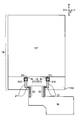
- FIG. 9 is an exploded perspective view of the liquid crystal display device 169.
- 10 is a plan view of the liquid crystal display panel 119 and the like included in the liquid crystal display device 169 shown in FIG. 9, and
- FIG. 8 is a cross-sectional view taken along the line EE ′ of the liquid crystal display device 169 shown in FIG. .
- the liquid crystal display device 169 includes a liquid crystal display panel 119 and a backlight unit 139 that irradiates the liquid crystal display panel 119 with light. Further, as shown in FIGS. 7 to 9, an LED (Light Emitting Diode) 131 is mounted on an FPC (Flexible Printed Circuits) substrate 116 attached to the liquid crystal display panel 119, and the light emitting surface 131 L of the LED 131 is the light guide plate 132. Facing the side surface 132S.
- FPC Flexible Printed Circuits
- the FPC board 116 In the liquid crystal display device 169 having such an internal structure, the FPC board 116 must be wound from one side of the liquid crystal display panel 119 to the other side in the vicinity of the end of the liquid crystal display panel 119. Further, as shown in FIG. 11 which is another example of FIG. 8, the FPC board 116 may be wound from one side of the liquid crystal display panel 119 to the other side so as to surround the built-in frame 170.
- a repulsive force is generated in the FPC board 116 that is bent due to winding, and due to this, the side surface (light receiving surface) 132S of the light guide plate 132 is caused.
- the position of the LED 131 may deviate from the desired position (in short, the positional accuracy of the LED 131 may be lowered).
- the positional deviation of the LED (light source) 131 with respect to the side surface 132S of the light guide plate 132 causes a light amount unevenness in the light from the backlight unit 139. As a result, the display quality of the liquid crystal display device 169 decreases. It also contributes.
- Patent Document 1 discloses a liquid crystal display device 169 that prevents such a problem.
- a concave portion 172 that accommodates a pin 171 formed on the light emitting surface 131L of the LED 131 is formed on the side surface 132S of the light guide plate 132.
- the LED 131 is immovable with respect to the light guide plate 132 due to the fit between the pin 171 formed on the LED 131 and the recess 172 formed on the light guide plate 132.
- the FPC board 116 is wound around the end of the liquid crystal display panel 119 from one side of the liquid crystal display panel 119 to the other side. Therefore, a repulsive force is generated in the FPC board 116.
- Such a repulsive force may cause the LED 131 to fluctuate, but may cause the liquid crystal display panel 119 to fluctuate.
- the liquid crystal display panel 119 may be lifted from the backlight unit 139 by a repulsive force. When such a floating phenomenon occurs, the display quality of the liquid crystal display device 169 is degraded.
- An object of the present invention is to provide a liquid crystal display device that prevents deterioration in display quality by simplifying the internal structure.
- the liquid crystal display device includes a liquid crystal display panel having a plurality of sandwiching substrates that sandwich the liquid crystal, and a backlight unit that is covered by the liquid crystal display panel and has a light guide plate that irradiates light to the liquid crystal display panel.
- the holding substrate closest to the light guide plate in the liquid crystal display panel is the first holding substrate and the substrate surface of the first holding substrate facing the light guide plate is the outer substrate surface, A light source for supplying light to the light plate is attached to the first sandwich substrate, and its light emitting surface is positioned on the outer substrate surface side.
- the light source is not attached to a flexible member such as an FPC board, but is directly attached to the first sandwich substrate included in the liquid crystal display panel.
- a flexible member such as an FPC board
- the light source is attached to the 1st clamping board
- substrate which does not have flexibility, it is hard to fluctuate. Therefore, the display quality deterioration of the liquid crystal display device due to the fluctuation of the light source is prevented.
- the light source is mounted on the outer substrate surface of the first sandwich substrate.
- the electrode of the light source is located on the outer substrate surface, and the panel wiring for passing current is mounted on the sandwich substrate surface which is the substrate surface on the back side of the outer substrate surface, and the first sandwich
- the substrate is preferably formed with a through hole that extends the panel wiring from the sandwich substrate surface to the outer substrate surface.
- the panel wiring extends to the outer substrate surface through the through hole and is connected to the electrode of the light source. Therefore, light can be emitted even if the light source is not mounted on an FPC board or the like.
- a part of the light source may be buried in an embedding hole penetrating the first sandwiching substrate.
- the light source when the light source is mounted in this way, it is desirable that it be as follows. That is, in the liquid crystal display device, panel wiring for passing current is mounted on the sandwich substrate surface, which is the substrate surface on the back side of the outer substrate surface, and the electrode of the light source is part of the light source buried in the embedded hole. It is desirable to be formed and positioned on the sandwich substrate surface.
- the electrode of the light source is connected to the panel wiring on the sandwich substrate surface of the first sandwich substrate, and the light source can emit light by the current flowing through it.
- the light source is attached to the highly stable first sandwich substrate that does not bend, a separate member (FPC substrate or the like) dedicated to the attachment of the light source becomes unnecessary, and the internal structure of the liquid crystal display device is simplified. become.
- FIG. 3 is a cross-sectional view taken along line A-A ′ of the liquid crystal display device shown in FIG. 2.
- FIG. 3 is an exploded perspective view of a liquid crystal display device. These are top views, such as a liquid crystal display panel contained in the liquid crystal display device shown by FIG.
- FIG. 6 is a cross-sectional view taken along line B-B ′ of the liquid crystal display device shown in FIG. 5.
- FIG. 3 is an exploded perspective view showing another example of the liquid crystal display device shown in FIG. 2.
- FIG. 6 is a plan view of a liquid crystal display panel and the like included in the liquid crystal display device shown in FIG. 5.
- FIG. 10 is a cross-sectional view taken along line E-E ′ of the conventional liquid crystal display device shown in FIG. 9.
- FIG. 6 is an exploded perspective view of a conventional liquid crystal display device.
- FIG. 10 is a plan view of a liquid crystal display panel and the like included in the conventional liquid crystal display device shown in FIG. 9.
- FIG. 12 is a cross-sectional view of another liquid crystal display device different from the conventional liquid crystal display device shown in FIGS.
- FIG. 2 is an exploded perspective view of the liquid crystal display device 69
- FIG. 3 is a plan view of the liquid crystal display panel 19 and the like included in the liquid crystal display device 69 shown in FIG.
- FIG. 1 is a cross-sectional view taken along line A-A ′ of the liquid crystal display device 69 shown in FIG.
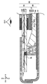
- the liquid crystal display device 69 includes a liquid crystal display panel 19, a backlight unit 39, and a housing HG that sandwiches them (the housing HG covering the liquid crystal display panel 19 includes a front housing HG1, The housing HG that supports the backlight unit 39 is referred to as a back housing HG2.
- the liquid crystal display panel 19 includes an active matrix substrate 11, a counter substrate 12, and polarizing films 13 and 13 that sandwich both the substrates 11 and 12.
- the active matrix substrate (first sandwich substrate) 11 is a substrate including a switching element such as a TFT for controlling liquid crystal (Thin Film Transistor) (the TFT is omitted in the drawing for convenience).
- a switching element such as a TFT for controlling liquid crystal (Thin Film Transistor) (the TFT is omitted in the drawing for convenience).
- the counter substrate (second sandwich substrate) 12 is a substrate including a color filter CF for coloring, and is bonded to the active matrix substrate 11 via a sealing material (not shown). Then, liquid crystal (not shown) is injected into the gap between the two substrates 11 and 12.
- a liquid crystal drive control LSI (Large Scale Integration) 15 is mounted on the exposed surface 11NE which is a part of the sandwich substrate surface 11N in the active matrix substrate 11 that is not covered by the counter substrate 12.
- the liquid crystal drive control LSI 15 is mounted, but the present invention is not limited to this.
- discrete components such as capacitors and resistors may be mounted together with the liquid crystal drive control LSI 15.
- the liquid crystal drive control LSI 15 is built in the liquid crystal display panel 19, there may be a case where only discrete components are mounted on the exposed surface 11NE, or nothing is mounted.
- a flexible FPC (Flexible Printed Circuits) substrate 16 having flexibility is attached to the exposed surface 11NE of the active matrix substrate 11 via an adhesive.
- the FPC board 16 and various elements are connected via the panel wiring 21 mounted on the exposed surface 11NE (note that the board wiring 22 and the panel wiring 21 in the FPC board 16 are connected, so that the current can be It flows to various elements through wiring 21 and 22).
- the polarizing films 13 and 13 are positioned so as to sandwich both the substrates 11 and 12, thereby adjusting the direction of light incident on the liquid crystal display panel 19 and light emitted from the liquid crystal display panel 19.
- the liquid crystal display panel 19 described above is a transmissive or transflective non-light emitting display panel, and thus exhibits a display function by receiving light from the backlight unit 39 (backlight light). Therefore, if the light from the backlight unit 39 can uniformly irradiate the entire surface of the liquid crystal display panel 19, the display quality of the liquid crystal display panel 19 is improved.
- the backlight unit 39 covered by the liquid crystal display panel 19 includes an LED (Light Emitting Diode) 31, a light guide plate 32, a reflection sheet 33, a diffusion sheet 34, and optical sheets 35 and 36.
- LED Light Emitting Diode
- the LED 31 is a light emitting element (point light source) having an electrode 31E, and emits light by receiving a current supply through the electrode 31E (the LED 31 mounting position will be described in detail later).
- the backlight unit 39 has a plurality of LEDs 31 mounted thereon, and it is further desirable that the LEDs 31 be arranged in a line.
- the direction in which the LEDs 31 are arranged is referred to as a parallel direction P).
- the light guide plate 32 is a plate-like member having a side surface 32S and a top surface 32U and a bottom surface 32B positioned so as to sandwich the side surface 32S. Then, one surface (light receiving surface) of the side surface 32 ⁇ / b> S faces the light emitting surface 31 ⁇ / b> L of the LED 31 to receive light from the LED 31. The received light is mixed inside the light guide plate 32 and is emitted outward from the top surface 32U as planar light.
- the reflection sheet 33 is positioned so as to be covered by the light guide plate 32. Then, one surface of the reflection sheet 33 facing the bottom surface 32B of the light guide plate 32 becomes a reflection surface. Therefore, this reflection surface reflects the light from the LED 31 and the light propagating through the light guide plate 32 so as to return to the light guide plate 32 (specifically, through the bottom surface 32B of the light guide plate 32) without leaking.
- the diffusion sheet 34 is positioned so as to cover the top surface 32U of the light guide plate 32, diffuses the planar light from the light guide plate 32, and spreads the light throughout the liquid crystal display panel 19 (Note that this diffusion sheet) 34 and the optical sheets 35 and 36 are collectively referred to as an optical sheet group 37).
- the optical sheets 35 and 36 are, for example, sheets having a prism shape in the sheet surface and deflecting the light radiation characteristic, and are positioned so as to cover the diffusion sheet 34. Therefore, the optical sheets 35 and 36 collect the light traveling from the diffusion sheet 34 and improve the luminance. In addition, the divergence direction of each light condensed by the optical sheet 35 and the optical sheet 36 has a crossing relationship.
- the reflection sheet 33, the light guide plate 32, the diffusion sheet 34, and the optical sheets 35 and 36 are stacked in this order. Therefore, the direction in which these members are stacked is defined as the overlapping direction Q, and the direction perpendicular to the parallel direction P of the LEDs 31 and the overlapping direction Q is defined as the direction R.
- the mounting position of the LED 31 will be described in detail.
- the liquid crystal display panel 19 is a transmissive or transflective type
- the light of the backlight unit 39 is irradiated from the back side of the display surface of the liquid crystal display panel 19 that is visually recognized by the user (Note that EYE in the drawing is Means the eyes of the user). That is, the counter substrate 12 of the liquid crystal display panel 19 becomes a substrate that is visible to the user, and the light from the backlight unit 39 is irradiated to the active matrix substrate 11 located on the back side of the counter substrate 12.
- the light from the backlight unit 39 is applied to the outer substrate surface 11T, which is a substrate surface that is not covered with the counter substrate 12 by the active matrix substrate 11.
- the outer substrate surface 11T which is a substrate surface that is not covered with the counter substrate 12 by the active matrix substrate 11.
- the light from the backlight unit 39 is applied to the outer substrate surface 11T, which is a substrate surface that is not covered with the counter substrate 12 by the active matrix substrate 11.
- the substrates 11 and 12 included in the liquid crystal display panel 19 light is incident from the outer substrate surface 11T facing the light guide plate 32 in the active matrix substrate 11 closest to the light guide plate 32.
- the top surface (light emitting surface) 32 U of the light guide plate 32 in the backlight unit 39 is covered with the active matrix substrate 11 of the liquid crystal display panel 19. Then, the side surface 32S of the light guide plate 32 and the outer substrate surface 11T of the active matrix substrate 11 (more specifically, the outer substrate surface 11T that does not overlap the top surface 32U of the light guide plate 32) approach each other with their surface directions crossing each other. become.
- the LED 31 is attached to the outer substrate surface 11T of the active matrix substrate 11 close to the side surface 32S with the light emitting surface 31L facing the side surface 32S of the light guide plate 32 while the light emitting surface 31L is positioned on the outer substrate surface side 11T. (Implemented).
- the internal structure of the liquid crystal display device 69 can be simplified. (In short, since the LEDs 31 are mounted on the liquid crystal display device 69, it is complicated. No internal structure is required).
- the LED 31 is not mounted on a highly flexible member such as the FPC board 16 but mounted on the active matrix board 11 having high rigidity. Therefore, the positional accuracy of the LED 31 is increased.
- the LED 31 mounted on the outer substrate surface 11T of the active matrix substrate 11 is more accurate than the accuracy with which the LED 31 mounted on the FPC substrate 16 is positioned at a predetermined position with respect to the side surface 32S of the light guide plate 32.
- the accuracy of being positioned at a predetermined position with respect to the side surface 32S of this is higher.
- the FPC board 16 when the LED 31 is mounted on the FPC board 16 connected to the exposed surface 11NE of the active matrix substrate 11, the FPC board 16 must be wound from the exposed surface 11NE to the outer substrate surface 11T. Then, a repulsive force is generated in the FPC board 16 bent by the winding, and this may cause a problem that the liquid crystal display panel 19 is displaced (the liquid crystal display device 19 is lifted from the backlight unit 39). Further, the LED 31 itself mounted on the FPC board 16 may fluctuate with respect to the side surface 32S of the light guide plate 32 due to the repulsive force generated in the FPC board 16.
- a current flowing through the substrate wiring 22 of the FPC board 16 connected to the exposed surface 11NE of the active matrix substrate 11 and the panel wiring 21 connected to the substrate wiring 22 is mounted on the outer substrate surface 11T of the active matrix substrate 11.
- the through hole HL is formed. That is, a through hole HL penetrating from the sandwiching substrate surface 11N (more specifically, the exposed surface 11NE) of the active matrix substrate 11 to the outer substrate surface 11T is formed.
- the panel wiring 21 on the exposed surface 11NE of the active matrix substrate 11 extends to the outer substrate surface 11T through the through hole HL formed on the exposed surface 11NE, and the electrode of the LED 31 It leads to 31E. Therefore, even if the LED 31 is mounted on the active matrix substrate 11, the current flowing through the substrate wiring 22 of the FPC board 16 reaches the electrode 31E of the LED 31 via the panel wiring 21, and the LED 31 can emit light.
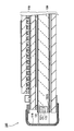
- FIG. 5 is an exploded perspective view of the liquid crystal display device 69
- FIG. 6 is a plan view of the liquid crystal display panel 19 and the like included in the liquid crystal display device 69 shown in FIG. 4 is a cross-sectional view taken along line B-B ′ shown in FIG.
- the active matrix substrate 11 is formed with holes (embedded holes) BL penetrating from the sandwiching substrate surface 11N (more specifically, the exposed surface 11NE) to the outer substrate surface 11T.
- the hole area of the embedded hole BL is an area that can accommodate the LED 31. More specifically, when the light emitting surface 31L is one of the side surfaces of the LED 31, the hole area of the embedded hole BL is larger than the outer peripheral area surrounding the entire side surface of the LED 31. As a result, the LED 31 can be embedded in the embedded hole BL.
- the LED 31 has the light emitting surface 31L facing the side surface (light receiving surface) 32S of the light guide plate 32, and the bottom surface 31B side (ie, a part of the LED 31), which is a surface other than its own side surface, such as the light emitting surface 31L.
- the adhesive material connects the LED 31 partially embedded in the buried hole BL and the active matrix substrate 11.
- the LED 31 is attached to the active matrix substrate 11, and the light emitting surface 31L of the LED 31 is active.
- the matrix substrate 11 is located on the outer substrate surface 11T side. Therefore, even in such a liquid crystal display device 69, as described above, the internal structure of the liquid crystal display device 69 is simplified, the positional accuracy of the LEDs 31 is improved, the positional deviation of the liquid crystal display panel 19 is prevented, and the liquid crystal display device A cost reduction of 69 is achieved.
- the electrode 31E of the LED 31 is preferably formed on a part of the LED 31 buried in the embedding hole BL, for example, the bottom surface 31B of the LED 31 and positioned on the sandwiching substrate surface 11N.
- the electrode 31E of the LED 31 is connected to the panel wiring 21 on the sandwiching substrate surface 11N of the active matrix substrate 11, and the LED 31 emits light by a current flowing from the substrate wiring 22 further connected to the panel wiring 21. It becomes possible.
- the embedded hole BL may not have a hole area enough to embed the LED 31 in some cases.
- the electrode 31E formed on the bottom surface 31B of the LED 31 is embedded in the embedded hole BL, and the LED 31 has the light emitting surface 31L on the light guide plate 32. May be directed to the side surface 32S.
- the LED 31 is attached to the active matrix substrate 11, and the light emitting surface 31L of the LED 31 is located on the outer substrate surface 11T side of the active matrix substrate 11.
- the internal structure of the liquid crystal display device 69 is simplified, the positional accuracy of the LEDs 31 is improved, the positional deviation of the liquid crystal display panel 19 is prevented, and the liquid crystal display A cost reduction of the device 69 is achieved.
- liquid crystal display device 69 was equipped with the liquid crystal display panel 19 incorporating the active matrix substrate 11, it is not limited to this.
- a passive liquid crystal display device 69 equipped with a liquid crystal display panel 19 including a substrate that does not use a switching element may be used instead of such an active liquid crystal display device 69.
Landscapes
- Physics & Mathematics (AREA)
- General Physics & Mathematics (AREA)
- Optics & Photonics (AREA)
- Nonlinear Science (AREA)
- Mathematical Physics (AREA)
- Chemical & Material Sciences (AREA)
- Crystallography & Structural Chemistry (AREA)
- Liquid Crystal (AREA)
- Planar Illumination Modules (AREA)
- Devices For Indicating Variable Information By Combining Individual Elements (AREA)
Abstract
Description
実施の一形態について、図面に基づいて説明すれば、以下の通りである。なお、便宜上、ハッチングや部材符号等を省略する場合もあるが、かかる場合、他の図面を参照するものとする。また、図面上での黒丸は紙面に対し垂直方向を意味する。
なお、本発明は上記の実施の形態に限定されず、本発明の趣旨を逸脱しない範囲で、種々の変更が可能である。
11N 対向基板に向くアクティブマトリックス基板の基板面である
挟持基板面
11T アクティブマトリックス基板の挟持基板面の裏側の基板面で
ある外基板面
11NE アクティブマトリックス基板の挟持基板面の一部分である露
出面
HL スルーホール
BL 埋込孔
12 対向基板
12N アクティブマトリックス基板に向く対向基板の基板面である
挟持基板面
12T 対向基板の挟持基板面の裏側の基板面である外基板面
13 偏光フィルム
15 LSI
16 FPC基板
19 液晶表示パネル
21 パネル配線
22 基板配線
31 LED(光源)
31L LEDの発光面
31B LEDの底面
32 導光板
32U 導光板の天面
32B 導光板の底面
32S 導光板の側面
39 バックライトユニット
69 液晶表示装置
Claims (5)
- 液晶を挟む複数の挟持基板を有する液晶表示パネルと、
上記液晶表示パネルによって覆われるとともに、その液晶表示パ
ネルに対して光を照射する導光板を有するバックライトユニットと、
を含む液晶表示装置にあって、
上記液晶表示パネルで上記導光板に最も近い上記挟持基板を第1挟持基板とし、その第1挟持基板の基板面で上記導光板に向くほうの基板面を外基板面とすると、
上記導光板に光を供給する光源は、上記第1挟持基板に取り付けられ、自身の発光面を上記外基板面側に位置させる液晶表示装置。 - 上記光源が、上記第1挟持基板の上記外基板面に実装される請求項1に記載の液晶表示装置。
- 上記外基板面に、上記光源の電極が位置し、
上記外基板面の裏側の基板面である挟持基板面には、電流を流すパネル配線が実装されており、
上記第1挟持基板には、上記パネル配線を、上記挟持基板面から上記外基板面まで延長させるスルーホールが形成される請求項2に記載の液晶表示装置。 - 上記光源の一部が、上記第1挟持基板を貫通する埋込孔に埋没する請求項1に記載の液晶表示装置。
- 上記外基板面の裏側の基板面である挟持基板面には、電流を流すパネル配線が実装されており、
上記光源の電極は、上記埋込孔に埋まる上記光源の一部に形成され、上記挟持基板面に位置する請求項4に記載の液晶表示装置。
Priority Applications (6)
| Application Number | Priority Date | Filing Date | Title |
|---|---|---|---|
| CN2009801226801A CN102067022B (zh) | 2008-07-08 | 2009-04-07 | 液晶显示装置 |
| EP09794239A EP2299316B1 (en) | 2008-07-08 | 2009-04-07 | Liquid crystal display device |
| JP2010519675A JP5221657B2 (ja) | 2008-07-08 | 2009-04-07 | 液晶表示装置 |
| RU2010153857/28A RU2473940C2 (ru) | 2008-07-08 | 2009-04-07 | Жидкокристаллическое дисплейное устройство |
| US13/002,654 US8373824B2 (en) | 2008-07-08 | 2009-04-07 | Liquid crystal display device |
| BRPI0915733A BRPI0915733A2 (pt) | 2008-07-08 | 2009-04-07 | dispositivo de vídeo de cristal líquido |
Applications Claiming Priority (2)
| Application Number | Priority Date | Filing Date | Title |
|---|---|---|---|
| JP2008-177555 | 2008-07-08 | ||
| JP2008177555 | 2008-07-08 |
Publications (1)
| Publication Number | Publication Date |
|---|---|
| WO2010004792A1 true WO2010004792A1 (ja) | 2010-01-14 |
Family
ID=41506914
Family Applications (1)
| Application Number | Title | Priority Date | Filing Date |
|---|---|---|---|
| PCT/JP2009/057088 Ceased WO2010004792A1 (ja) | 2008-07-08 | 2009-04-07 | 液晶表示装置 |
Country Status (7)
| Country | Link |
|---|---|
| US (1) | US8373824B2 (ja) |
| EP (1) | EP2299316B1 (ja) |
| JP (1) | JP5221657B2 (ja) |
| CN (1) | CN102067022B (ja) |
| BR (1) | BRPI0915733A2 (ja) |
| RU (1) | RU2473940C2 (ja) |
| WO (1) | WO2010004792A1 (ja) |
Cited By (3)
| Publication number | Priority date | Publication date | Assignee | Title |
|---|---|---|---|---|
| WO2012056660A1 (ja) * | 2010-10-25 | 2012-05-03 | シャープ株式会社 | 液晶表示装置及びその製造方法 |
| WO2012169268A1 (ja) * | 2011-06-07 | 2012-12-13 | シャープ株式会社 | 表示装置及びテレビジョン受信機 |
| JP2012256073A (ja) * | 2012-09-05 | 2012-12-27 | Sharp Corp | 表示装置及びテレビ受信装置 |
Families Citing this family (3)
| Publication number | Priority date | Publication date | Assignee | Title |
|---|---|---|---|---|
| US9841645B2 (en) | 2015-04-02 | 2017-12-12 | Himax Display, Inc. | Display device |
| EP3086171B1 (en) * | 2015-04-21 | 2018-03-14 | Himax Display, Inc. | Display device |
| KR102627114B1 (ko) * | 2016-12-30 | 2024-01-19 | 엘지디스플레이 주식회사 | 액정표시장치 |
Citations (2)
| Publication number | Priority date | Publication date | Assignee | Title |
|---|---|---|---|---|
| JP2001330830A (ja) | 2000-05-23 | 2001-11-30 | Seiko Epson Corp | 液晶装置及び電子機器 |
| JP2007171459A (ja) * | 2005-12-21 | 2007-07-05 | Citizen Holdings Co Ltd | 表示装置及びその製造方法 |
Family Cites Families (11)
| Publication number | Priority date | Publication date | Assignee | Title |
|---|---|---|---|---|
| JP3697925B2 (ja) * | 1999-02-26 | 2005-09-21 | セイコーエプソン株式会社 | 電気光学装置 |
| RU2183864C2 (ru) | 1999-08-04 | 2002-06-20 | ОПТИВА, Инк. | Модуль отображения информации |
| JP3987257B2 (ja) | 1999-12-10 | 2007-10-03 | ローム株式会社 | 液晶表示装置 |
| JP4439084B2 (ja) | 2000-06-14 | 2010-03-24 | 日東電工株式会社 | 液晶表示装置 |
| KR20050107033A (ko) * | 2004-05-07 | 2005-11-11 | 삼성전자주식회사 | 발광 다이오드 모듈 및 이를 구비한 액정표시장치 |
| CN2785066Y (zh) * | 2005-02-18 | 2006-05-31 | 群康科技(深圳)有限公司 | 显示模组 |
| JP4244942B2 (ja) * | 2005-03-08 | 2009-03-25 | セイコーエプソン株式会社 | 液晶装置、照明装置、および電子機器 |
| JP2007121597A (ja) * | 2005-10-27 | 2007-05-17 | Fujifilm Corp | 液晶表示装置 |
| US7534025B2 (en) * | 2006-08-25 | 2009-05-19 | Philips Lumiled Lighting Company, Llc | Thin backlight with flipped light emitting diode |
| JP2008170739A (ja) * | 2007-01-12 | 2008-07-24 | Hitachi Displays Ltd | 液晶表示装置 |
| US20110170033A1 (en) | 2008-09-25 | 2011-07-14 | Sharp Kabushiki Kaisha | Liquid crystal display device and manufacturing method therefor |
-
2009
- 2009-04-07 RU RU2010153857/28A patent/RU2473940C2/ru not_active IP Right Cessation
- 2009-04-07 US US13/002,654 patent/US8373824B2/en not_active Expired - Fee Related
- 2009-04-07 EP EP09794239A patent/EP2299316B1/en not_active Not-in-force
- 2009-04-07 BR BRPI0915733A patent/BRPI0915733A2/pt not_active IP Right Cessation
- 2009-04-07 CN CN2009801226801A patent/CN102067022B/zh not_active Expired - Fee Related
- 2009-04-07 WO PCT/JP2009/057088 patent/WO2010004792A1/ja not_active Ceased
- 2009-04-07 JP JP2010519675A patent/JP5221657B2/ja not_active Expired - Fee Related
Patent Citations (2)
| Publication number | Priority date | Publication date | Assignee | Title |
|---|---|---|---|---|
| JP2001330830A (ja) | 2000-05-23 | 2001-11-30 | Seiko Epson Corp | 液晶装置及び電子機器 |
| JP2007171459A (ja) * | 2005-12-21 | 2007-07-05 | Citizen Holdings Co Ltd | 表示装置及びその製造方法 |
Non-Patent Citations (1)
| Title |
|---|
| See also references of EP2299316A4 |
Cited By (5)
| Publication number | Priority date | Publication date | Assignee | Title |
|---|---|---|---|---|
| WO2012056660A1 (ja) * | 2010-10-25 | 2012-05-03 | シャープ株式会社 | 液晶表示装置及びその製造方法 |
| WO2012169268A1 (ja) * | 2011-06-07 | 2012-12-13 | シャープ株式会社 | 表示装置及びテレビジョン受信機 |
| JP2012256983A (ja) * | 2011-06-07 | 2012-12-27 | Sharp Corp | 表示装置及びテレビ受信装置 |
| US9182534B2 (en) | 2011-06-07 | 2015-11-10 | Sharp Kabushiki Kaisha | Display device and television receiver |
| JP2012256073A (ja) * | 2012-09-05 | 2012-12-27 | Sharp Corp | 表示装置及びテレビ受信装置 |
Also Published As
| Publication number | Publication date |
|---|---|
| RU2010153857A (ru) | 2012-08-20 |
| JPWO2010004792A1 (ja) | 2011-12-22 |
| BRPI0915733A2 (pt) | 2015-10-27 |
| CN102067022A (zh) | 2011-05-18 |
| US8373824B2 (en) | 2013-02-12 |
| RU2473940C2 (ru) | 2013-01-27 |
| EP2299316B1 (en) | 2013-03-13 |
| US20110109841A1 (en) | 2011-05-12 |
| JP5221657B2 (ja) | 2013-06-26 |
| EP2299316A4 (en) | 2012-01-04 |
| CN102067022B (zh) | 2013-02-06 |
| EP2299316A1 (en) | 2011-03-23 |
Similar Documents
| Publication | Publication Date | Title |
|---|---|---|
| CN101256305B (zh) | 背光组件和具有该背光组件的显示设备 | |
| CN103558705B (zh) | 液晶显示装置 | |
| US7581869B2 (en) | Backlight assembly and display device having the same | |
| JP5255960B2 (ja) | 液晶表示装置 | |
| KR101299130B1 (ko) | 액정표시장치 | |
| US20100220496A1 (en) | Display apparatus and method of assembling the same | |
| JP5221657B2 (ja) | 液晶表示装置 | |
| KR20140106905A (ko) | 액정표시장치 | |
| KR100786479B1 (ko) | 평판표시장치 및 이를 이용한 휴대용 표시기기 | |
| KR102459047B1 (ko) | 터치패널 부착형 액정표시장치 | |
| US9395484B2 (en) | Display device | |
| US9182536B2 (en) | Light-source device and display device | |
| US9690039B2 (en) | Light source device and display device | |
| KR20120136879A (ko) | 액정표시장치 | |
| JP2009004214A (ja) | 基板、基板ユニット、バックライトユニット、および液晶表示装置 | |
| KR101920760B1 (ko) | 백라이트 유닛을 포함하는 액정표시장치모듈 | |
| KR20180060525A (ko) | 액정표시장치 | |
| KR20170117695A (ko) | 두 개의 프리즘 시트를 포함하는 액정 표시 장치 | |
| US20130258242A1 (en) | Liquid crystal display device | |
| KR20130025765A (ko) | 액정표시장치 | |
| KR20180054263A (ko) | 백라이트 유닛 및 이를 포함하는 표시장치 | |
| KR20170117697A (ko) | 몰드 프레임을 포함하는 액정 표시 장치 | |
| KR101274795B1 (ko) | 액정 표시 장치 및 그 조립 방법 | |
| KR20170126269A (ko) | 광학 시트를 포함하는 액정 표시 장치 | |
| KR20150037237A (ko) | Led 백라이트를 구비한 액정표시소자 |
Legal Events
| Date | Code | Title | Description |
|---|---|---|---|
| WWE | Wipo information: entry into national phase |
Ref document number: 200980122680.1 Country of ref document: CN |
|
| 121 | Ep: the epo has been informed by wipo that ep was designated in this application |
Ref document number: 09794239 Country of ref document: EP Kind code of ref document: A1 |
|
| WWE | Wipo information: entry into national phase |
Ref document number: 2010519675 Country of ref document: JP |
|
| WWE | Wipo information: entry into national phase |
Ref document number: 2009794239 Country of ref document: EP |
|
| WWE | Wipo information: entry into national phase |
Ref document number: 27/CHENP/2011 Country of ref document: IN |
|
| WWE | Wipo information: entry into national phase |
Ref document number: 13002654 Country of ref document: US |
|
| NENP | Non-entry into the national phase |
Ref country code: DE |
|
| WWE | Wipo information: entry into national phase |
Ref document number: 2010153857 Country of ref document: RU |
|
| ENP | Entry into the national phase |
Ref document number: PI0915733 Country of ref document: BR Kind code of ref document: A2 Effective date: 20110110 |