WO2010010954A1 - ドットマトリックス型情報表示用パネル - Google Patents
ドットマトリックス型情報表示用パネル Download PDFInfo
- Publication number
- WO2010010954A1 WO2010010954A1 PCT/JP2009/063289 JP2009063289W WO2010010954A1 WO 2010010954 A1 WO2010010954 A1 WO 2010010954A1 JP 2009063289 W JP2009063289 W JP 2009063289W WO 2010010954 A1 WO2010010954 A1 WO 2010010954A1
- Authority
- WO
- WIPO (PCT)
- Prior art keywords
- display panel
- information display
- dot matrix
- matrix type
- type information
- Prior art date
- Legal status (The legal status is an assumption and is not a legal conclusion. Google has not performed a legal analysis and makes no representation as to the accuracy of the status listed.)
- Ceased
Links
Images





Classifications
-
- G—PHYSICS
- G09—EDUCATION; CRYPTOGRAPHY; DISPLAY; ADVERTISING; SEALS
- G09F—DISPLAYING; ADVERTISING; SIGNS; LABELS OR NAME-PLATES; SEALS
- G09F9/00—Indicating arrangements for variable information in which the information is built-up on a support by selection or combination of individual elements
- G09F9/30—Indicating arrangements for variable information in which the information is built-up on a support by selection or combination of individual elements in which the desired character or characters are formed by combining individual elements
- G09F9/37—Indicating arrangements for variable information in which the information is built-up on a support by selection or combination of individual elements in which the desired character or characters are formed by combining individual elements being movable elements
- G09F9/372—Indicating arrangements for variable information in which the information is built-up on a support by selection or combination of individual elements in which the desired character or characters are formed by combining individual elements being movable elements the positions of the elements being controlled by the application of an electric field
-
- G—PHYSICS
- G02—OPTICS
- G02F—OPTICAL DEVICES OR ARRANGEMENTS FOR THE CONTROL OF LIGHT BY MODIFICATION OF THE OPTICAL PROPERTIES OF THE MEDIA OF THE ELEMENTS INVOLVED THEREIN; NON-LINEAR OPTICS; FREQUENCY-CHANGING OF LIGHT; OPTICAL LOGIC ELEMENTS; OPTICAL ANALOGUE/DIGITAL CONVERTERS
- G02F1/00—Devices or arrangements for the control of the intensity, colour, phase, polarisation or direction of light arriving from an independent light source, e.g. switching, gating or modulating; Non-linear optics
- G02F1/01—Devices or arrangements for the control of the intensity, colour, phase, polarisation or direction of light arriving from an independent light source, e.g. switching, gating or modulating; Non-linear optics for the control of the intensity, phase, polarisation or colour
- G02F1/165—Devices or arrangements for the control of the intensity, colour, phase, polarisation or direction of light arriving from an independent light source, e.g. switching, gating or modulating; Non-linear optics for the control of the intensity, phase, polarisation or colour based on translational movement of particles in a fluid under the influence of an applied field
- G02F1/166—Devices or arrangements for the control of the intensity, colour, phase, polarisation or direction of light arriving from an independent light source, e.g. switching, gating or modulating; Non-linear optics for the control of the intensity, phase, polarisation or colour based on translational movement of particles in a fluid under the influence of an applied field characterised by the electro-optical or magneto-optical effect
- G02F1/167—Devices or arrangements for the control of the intensity, colour, phase, polarisation or direction of light arriving from an independent light source, e.g. switching, gating or modulating; Non-linear optics for the control of the intensity, phase, polarisation or colour based on translational movement of particles in a fluid under the influence of an applied field characterised by the electro-optical or magneto-optical effect by electrophoresis
-
- G—PHYSICS
- G09—EDUCATION; CRYPTOGRAPHY; DISPLAY; ADVERTISING; SEALS
- G09F—DISPLAYING; ADVERTISING; SIGNS; LABELS OR NAME-PLATES; SEALS
- G09F9/00—Indicating arrangements for variable information in which the information is built-up on a support by selection or combination of individual elements
- G09F9/30—Indicating arrangements for variable information in which the information is built-up on a support by selection or combination of individual elements in which the desired character or characters are formed by combining individual elements
- G09F9/302—Indicating arrangements for variable information in which the information is built-up on a support by selection or combination of individual elements in which the desired character or characters are formed by combining individual elements characterised by the form or geometrical disposition of the individual elements
-
- G—PHYSICS
- G02—OPTICS
- G02F—OPTICAL DEVICES OR ARRANGEMENTS FOR THE CONTROL OF LIGHT BY MODIFICATION OF THE OPTICAL PROPERTIES OF THE MEDIA OF THE ELEMENTS INVOLVED THEREIN; NON-LINEAR OPTICS; FREQUENCY-CHANGING OF LIGHT; OPTICAL LOGIC ELEMENTS; OPTICAL ANALOGUE/DIGITAL CONVERTERS
- G02F1/00—Devices or arrangements for the control of the intensity, colour, phase, polarisation or direction of light arriving from an independent light source, e.g. switching, gating or modulating; Non-linear optics
- G02F1/01—Devices or arrangements for the control of the intensity, colour, phase, polarisation or direction of light arriving from an independent light source, e.g. switching, gating or modulating; Non-linear optics for the control of the intensity, phase, polarisation or colour
- G02F1/13—Devices or arrangements for the control of the intensity, colour, phase, polarisation or direction of light arriving from an independent light source, e.g. switching, gating or modulating; Non-linear optics for the control of the intensity, phase, polarisation or colour based on liquid crystals, e.g. single liquid crystal display cells
- G02F1/133—Constructional arrangements; Operation of liquid crystal cells; Circuit arrangements
- G02F1/1333—Constructional arrangements; Manufacturing methods
- G02F1/1343—Electrodes
- G02F1/134309—Electrodes characterised by their geometrical arrangement
- G02F1/134327—Segmented, e.g. alpha numeric display
-
- G—PHYSICS
- G02—OPTICS
- G02F—OPTICAL DEVICES OR ARRANGEMENTS FOR THE CONTROL OF LIGHT BY MODIFICATION OF THE OPTICAL PROPERTIES OF THE MEDIA OF THE ELEMENTS INVOLVED THEREIN; NON-LINEAR OPTICS; FREQUENCY-CHANGING OF LIGHT; OPTICAL LOGIC ELEMENTS; OPTICAL ANALOGUE/DIGITAL CONVERTERS
- G02F1/00—Devices or arrangements for the control of the intensity, colour, phase, polarisation or direction of light arriving from an independent light source, e.g. switching, gating or modulating; Non-linear optics
- G02F1/01—Devices or arrangements for the control of the intensity, colour, phase, polarisation or direction of light arriving from an independent light source, e.g. switching, gating or modulating; Non-linear optics for the control of the intensity, phase, polarisation or colour
- G02F1/165—Devices or arrangements for the control of the intensity, colour, phase, polarisation or direction of light arriving from an independent light source, e.g. switching, gating or modulating; Non-linear optics for the control of the intensity, phase, polarisation or colour based on translational movement of particles in a fluid under the influence of an applied field
- G02F1/1675—Constructional details
- G02F1/1679—Gaskets; Spacers; Sealing of cells; Filling or closing of cells
- G02F1/1681—Gaskets; Spacers; Sealing of cells; Filling or closing of cells having two or more microcells partitioned by walls, e.g. of microcup type
Definitions
- a plurality of cells partitioned by partition walls are formed between two opposing substrates at least one of which is transparent, a display medium configured as a particle group is disposed in the cell, and the display medium is electrically
- the present invention relates to a rectangular dot matrix type information display panel that is driven to display information such as an image.
- a plurality of cells partitioned by partition walls are formed between two opposing substrates, at least one of which is transparent, a display medium configured as a particle group is disposed in the cell, and the display medium is electrically driven.
- a rectangular dot matrix type information display panel for displaying information such as images is known (see, for example, Japanese Patent Laid-Open No. 2001-215537).
- a lattice shape, a honeycomb shape, or the like is proposed as the shape of the cells partitioned by the partition walls, and a rectangular dot is proposed as the electrode shape to be a pixel.
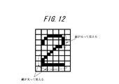
- FIG. 12 is a diagram showing an example in which cells are formed by using grid-like partition walls in the above-described conventional information display panel.
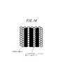
- FIG. 13 and FIG. 14 are diagrams showing examples in which cells are formed using honeycomb-shaped partition walls in the above-described conventional information display panel. In either example, only the partition walls are displayed so that the configuration of the partition walls can be clearly understood, and the substrate and electrodes necessary for configuring the information display panel are not shown.
- the examples shown in FIGS. 12 and 13 both show a state in which the numeral “2” is to be displayed. In the example shown in FIG. 14, three lines are to be displayed at equal intervals in the vertical direction. Shows the state.
- the object of the present invention is to solve the above-mentioned problems, and when displaying image information based on lines such as characters, the vertical and horizontal lines are not so noticeable, and the dots are not square, as in the case of honeycomb-shaped partition walls.
- An object of the present invention is to provide a dot matrix type information display panel that can express an image based on a line such as a sharp and natural character without appearing to collapse or causing interference fringes (moire).
- the dot matrix type information display panel of the present invention a plurality of cells partitioned by partition walls are formed between two opposing substrates at least one of which is transparent, and a display medium configured as a particle group is disposed in the cell
- the plurality of cells have at least a cell shape.
- a polygon cell having an even number of sides of 6 or more is used, and a plurality of cells having the polygon shape as a unit are regularly arranged and arranged in the display area.
- all of the partition walls of polygonal cells are connected at right angles, and the polygonal cell shape is any of L shape, step shape, and convex shape.
- the square pixel electrode pair size formed on the substrate is a square of 100 ⁇ m or more ⁇ 100 ⁇ m or more, the width of the partition wall is in the range of 5 ⁇ m to 50 ⁇ m, and the partition wall is formed by a photolithography method. There is.
- the plurality of cells are polygonal cells that are formed by connecting all the partition walls that have an even number of sides of at least six sides at right angles, and the plurality of cells in units of polygonal shapes
- the vertical and horizontal lines are not so noticeable, and the dots are not square, as in the case of honeycomb-shaped partition walls. It is possible to obtain an information display panel that can express an image based on a line such as a sharp and natural character without appearing to be broken or causing interference fringes (moire).
- partition area in the display area causes a decrease in the aperture ratio and a decrease in contrast.
- the partition area in the present invention example is 125% even when hexagonal cells are arranged in a honeycomb arrangement. There is no extreme decline.
- the intersections of the partition walls exist uniformly, increasing the strength against peeling.
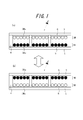
- (A), (b) is a figure which shows an example of the panel structure body of the dot matrix type information display panel of this invention, respectively.
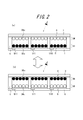
- (A), (b) is a figure which shows the other example of the panel structure body of the dot matrix type information display panel of this invention, respectively.
- (A), (b) is a figure which shows the further another example of the panel structure body of the dot matrix type information display panel of this invention, respectively.
- (A)-(g) is a figure for demonstrating an example of the polygon cell in the dot matrix type information display panel of this invention, respectively.
- (A)-(g) is a figure for demonstrating the other example of the polygon cell in the dot matrix type information display panel of this invention, respectively.
- (A)-(g) is a figure for demonstrating the further another example of the polygon cell in the dot matrix type information display panel of this invention, respectively.
- (A)-(g) is a figure for demonstrating the further another example of the polygon cell in the dot matrix type information display panel of this invention, respectively. It is a figure which shows the example using the step-shaped polygonal cell in the dot matrix type information display panel of this invention. It is a figure which shows the example using the step-shaped polygonal cell in the dot matrix type information display panel of this invention.
- (A), (b) is a figure for demonstrating an example of the board
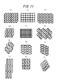
- (A)-(l) is a figure for demonstrating the polygonal cell formed of the partition in the Example of the dot matrix type information display panel of this invention, respectively. It is a figure which shows the example which formed the cell from the grid
- a display panel using a particle group containing chargeable particles as a display medium will be described.
- an electric field is applied to a display medium configured as a particle group including charged particles having optical reflectivity sealed in a space between two opposing substrates. Is granted.
- the display medium is attracted by an electric field force or a Coulomb force, and the display medium is moved by a change in the electric field direction, whereby information such as an image is displayed.
- the display panel so that the display medium can move uniformly and maintain the stability when the display information is rewritten or when the display information is continuously displayed.
- the force applied to the particles constituting the display medium in addition to the force attracting each other by the Coulomb force between the particles, an electric mirror image force between the electrode and the substrate, an intermolecular force, a liquid cross-linking force, gravity and the like can be considered.
- At least two types of display media configured as a particle group including particles having at least optical reflectance and chargeability are included.
- the electrode provided on the substrate 1 in each cell formed by the partition walls 4 is a white display medium 3W configured as a particle group and a black display medium 3B configured as a particle group including positively charged black particles 3Ba).
- 5 (line electrode) and the electrode 6 (line electrode) provided on the substrate 2 are opposed to each other, and the substrates 1, 2, Move vertically.
- the pixel electrode pair (one dot) and the cell are in a one-to-one correspondence. Then, as shown in FIG.
- the white display medium 3W is visually recognized by the observer to perform white display (white three dots), or as shown in FIG. 1 (b), the black display medium 3B. Is visually recognized by the observer, and black display (black three dots) is performed.
- the partition in front is abbreviate
- At least two types of display media (here, including negatively charged white particles 3Wa) configured as a particle group including particles having at least optical reflectance and chargeability are included.
- the electrode provided on the substrate 1 in each cell formed by the partition walls 4 is a white display medium 3W configured as a particle group and a black display medium 3B configured as a particle group including positively charged black particles 3Ba).
- 5 (pixel electrode with TFT) and an electrode 6 (common electrode) provided on the substrate 2 are moved perpendicularly to the substrates 1 and 2 in accordance with an electric field generated by applying a voltage.
- the pixel electrode pair (one dot) and the cell are in a one-to-one correspondence. Then, as shown in FIG.
- the white display medium 3W is visually recognized by the observer to perform white display (white 3 dots), or as shown in FIG. 2 (b), the black display medium 3B. Is visually recognized by the observer, and black display (black three dots) is performed.
- the partition in front is abbreviate
- a charged particle gas moving type display panel in which the cell space is filled with gas has been described.
- a charged particle liquid moving type (electrophoretic type) moving method using an insulating liquid is used instead of gas.
- a display panel instead of gas, a charged particle liquid moving type (electrophoretic type) moving method using an insulating liquid is used. It can also be a display panel.
- FIGS. 3A and 3B show an example of color display in which a display unit (1 dot) is constituted by three cells (pixels) each corresponding to a pixel electrode pair.
- a display unit (1 dot) is constituted by three cells (pixels) each corresponding to a pixel electrode pair.
- all of the cells 21-1 to 21-3 are filled with the white display medium 3W and the black display medium 3B as the display medium, and the first cell 21-1 is filled.
- a red color filter 22R is provided on the viewer side
- a green color filter 22G is provided on the viewer side of the second cell 21-2
- a blue color filter 22BL is provided on the viewer side of the third cell 21-3.
- the three cells (pixels) of the first cell 21-1, the second cell 21-2, and the third cell 21-3 constitute a display unit (1 dot).
- the information display panel according to the present invention is characterized by a square composed of opposed counter electrodes in which electrodes provided on one substrate overlap electrodes provided on the other substrate.
- a dot matrix type display panel having a shape of unit pixel (1 dot) the shape of a cell in which a particle group serving as a display medium is arranged is formed by connecting all the partition walls having even sides of 6 or more at right angles.
- the panel is formed by combining a plurality of unit cells having the same shape with rectangular cells.
- FIG. 4 (a) to 4 (g) are diagrams for explaining examples of polygonal cells in the dot matrix type information display panel of the present invention.
- the size of the quadrangle 11 serving as the basic unit of the polygonal cell shown in FIG. 4A is the same as the size of the pixel 15 consisting of the quadrangle shown in FIG.
- An arrangement example with the pixel 15 is shown.
- FIG. 4C an L-shaped polygonal cell 12 composed of three unit squares 11 is shown.
- FIG. 4D a stepped polygonal cell 12 composed of four unit squares 11 is shown.
- FIG. 4 (e) a step-shaped polygonal cell 12 composed of six unit squares 11 is shown.
- FIG. 4F a convex polygonal cell 12 composed of four unit squares 11 is shown.
- FIG. 4G an L-shaped polygon cell 12 composed of four unit squares 11 is shown.
- FIGS. 5A to 5G are diagrams for explaining other examples of polygonal cells in the dot matrix type information display panel of the present invention.
- the polygonal cell in the case where the size of the unit rectangle 11 serving as the basic unit of the polygonal cell shown in FIG. 5A is a quarter of the size of the pixel 15 shown in FIG.
- An arrangement example with the pixel 15 is shown.
- an L-shaped polygonal cell 12 composed of three unit squares 11 is shown.
- a step-shaped polygonal cell 12 composed of four unit squares 11 is shown.
- a step-shaped polygonal cell 12 composed of six unit squares 11 is shown.
- a convex polygonal cell 12 composed of four unit squares 11 is shown.
- an L-shaped polygonal cell 12 composed of four unit squares 11 is shown.
- FIG. 6 (a) to 6 (g) are diagrams for explaining still other examples of polygonal cells in the dot matrix type information display panel of the present invention.
- the size of the unit rectangle 11 consisting of a rectangle slightly longer in the vertical direction in FIG. 6A and the size of the pixel 15 consisting of a rectangle slightly longer in the vertical direction shown in FIG. Shows an arrangement example of the unit quadrangle 11 and the pixel 15 in the case where the same.
- FIG. 6C an L-shaped polygonal cell 12 composed of three unit squares 11 is shown.
- FIG. 6D a step-shaped polygonal cell 12 composed of four unit squares 11 is shown.
- a step-shaped polygonal cell 12 composed of six unit squares 11 is shown.
- a convex polygonal cell 12 composed of four unit squares 11 is shown.
- an L-shaped polygonal cell 12 composed of four unit squares 11 is shown.
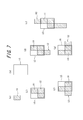
- FIGS. 7A to 7G are diagrams for explaining still another example of polygonal cells in the dot matrix information display panel of the present invention.
- the size of the unit quadrangle 11 made of a rectangle slightly longer in the vertical direction in the figure shown in FIG. 7A is the size of the pixel 15 made of a rectangle slightly longer in the vertical direction in FIG. 7B.
- positioning of the polygon cell and the pixel 15 in the case of 1/4 is shown.
- an L-shaped polygonal cell 12 composed of three unit squares 11 is shown.
- a stepped polygonal cell 12 composed of four unit squares 11 is shown.
- a step-shaped polygonal cell 12 composed of six unit squares 11 is shown.
- a convex polygonal cell 12 composed of four unit squares 11 is shown.
- an L-shaped polygonal cell 12 composed of four unit squares 11 is shown.
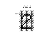
- FIG. 8 and FIG. 9 are diagrams each showing an example in which stepped polygonal cells are used in the dot matrix type information display panel of the present invention.
- the example shown in FIGS. 8 and 9 uses the same stepped polygonal cell 12. The difference is that in the example shown in FIG. 8, a plurality of step-shaped polygonal cells 12 are arranged in the vertical direction in the figure, whereas in the example shown in FIG. 9, the step-shaped polygonal cells 12 are shown in the figure.
- a plurality of polygonal cells 12 are arranged so as to be aligned in an oblique direction with a deviation from the vertical and horizontal directions. In either example, only the partition walls are displayed so that the configuration of the partition walls can be clearly understood, and the substrate and electrodes necessary for configuring the information display panel are not shown.
- FIG. 8 and FIG. 9 shows the following when comparing the display state of the dot matrix type information display panel of the present invention shown in FIGS. 8 and 9 with the display state of the conventional information display panel shown in FIGS.
- vertical and horizontal lines are not so conspicuous.
- the partition wall shape shown in FIG. 13 and FIG. 14 is a honeycomb shape, dots do not appear to be broken from a quadrangle, and interference fringes (moire) are not generated.
- the partition does not completely border the outer periphery of the character, a sharp and natural character can be expressed.
- the aperture ratio decreases and the contrast decreases.
- the partition wall area is about 125% as compared with the example in which hexagonal cells are arranged in a honeycomb, and the contrast is extremely high. There is no significant decline. The intersections of the partition walls exist uniformly, and the strength against peeling is increased at the junction between the top of the partition walls and the panel substrate.
- the width of the unit square 11 formed from the counter electrode pair that is, the width of the electrodes 5 and 6 is 100 ⁇ m or more. More preferably, the thickness is 200 ⁇ m or more. Further, if the area of the polygonal cell 12 is too large, the particle group as the display medium tends to be biased. Therefore, the configuration shown in FIGS. 4, 5, 6, and 7 is preferable in correspondence with the pixels.
- the substrate As for the substrate, at least one of the substrates is a transparent substrate 2 on which the color of the display medium can be confirmed from the outside of the information display panel, and a material having high visible light transmittance and good heat resistance is suitable.
- the substrate 1 may be transparent or opaque.
- substrate materials include polymer sheets such as polyethylene terephthalate, polyethylene naphthalate, polyethersulfone, polyethylene, polycarbonate, polyimide, and acrylic, flexible materials such as metal sheets, and glass and quartz.
- An inorganic sheet having no flexibility is mentioned.
- the thickness of the substrate is preferably 2 to 2000 ⁇ m, and more preferably 5 to 1000 ⁇ m. If it is too thin, it will be difficult to maintain the strength and uniformity of the distance between the substrates, and if it is thicker than 2000 ⁇ m, it will be a thin information display panel. Is inconvenient.
- electrode forming materials include metals such as aluminum, silver, nickel, copper, and gold, indium tin oxide (ITO), indium zinc oxide (IZO), indium oxide, aluminum-doped zinc oxide (AZO), conductive tin oxide, Conductive metal oxides such as antimony tin oxide (ATO) and conductive zinc oxide, and conductive polymers such as polyaniline, polypyrrole, and polythiophene are exemplified and appropriately selected and used.
- ITO indium tin oxide
- IZO indium zinc oxide
- AZO aluminum-doped zinc oxide
- Conductive metal oxides such as antimony tin oxide (ATO) and conductive zinc oxide
- conductive polymers such as polyaniline, polypyrrole, and polythiophene are exemplified and appropriately selected and used.
- a method for forming the electrode a method of forming the above-described materials into a thin film by sputtering, vacuum vapor deposition, CVD (chemical vapor deposition), coating, or the like, or a method of laminating metal foil (for example, rolled copper foil) Etc.), and a method in which a conductive agent is mixed with a solvent or a synthetic resin binder and applied.
- the electrode provided on the display surface side substrate 2 which is on the viewing side and needs to be transparent needs to be transparent, but the electrode provided on the back side substrate 1 does not need to be transparent.
- the above-mentioned material that can be patterned and is electrically conductive can be suitably used.
- the electrode thickness may be 0.01 to 10 ⁇ m, preferably 0.05 to 5 ⁇ m, as long as the conductivity is ensured and light transmittance is not hindered.
- the material and thickness of the electrode provided on the back side substrate 1 are the same as those of the electrode provided on the display surface side substrate described above, but need not be transparent.
- the partition 4 has a shape capable of forming the unit cell 12 described above.
- Examples of the method for forming the partition include a mold transfer method, a screen printing method, a sand blast method, a photolithography method, and an additive method. Any of these methods can be suitably used for the information display panel of the present invention, and among these, a photolithography method using a resist film and a mold transfer method are suitably used.
- the particle group is composed of these particles alone to form a display medium, or a particle group is composed of other particles together to form a display medium.
- the particles can contain a charge control agent, a colorant, an inorganic additive, and the like, if necessary, in the resin as the main component, as in the conventional case. Examples of resins, charge control agents, colorants, and other additives will be given below.
- the resin examples include urethane resin, urea resin, acrylic resin, polyester resin, acrylic urethane resin, acrylic urethane silicone resin, acrylic urethane fluororesin, acrylic fluororesin, silicone resin, acrylic silicone resin, epoxy resin, polystyrene resin, styrene Acrylic resin, polyolefin resin, butyral resin, vinylidene chloride resin, melamine resin, phenol resin, fluororesin, polycarbonate resin, polysulfone resin, polyether resin, polyamide resin and the like can be mentioned, and two or more kinds can be mixed.
- acrylic urethane resin, acrylic silicone resin, acrylic fluororesin, acrylic urethane silicone resin, acrylic urethane fluororesin, fluororesin, and silicone resin are suitable from the viewpoint of controlling the adhesive force with the substrate.
- the charge control agent is not particularly limited.
- the negative charge control agent include salicylic acid metal complexes, metal-containing azo dyes, metal-containing oil-soluble dyes (including metal ions and metal atoms), and quaternary ammonium salt systems. Examples thereof include compounds, calixarene compounds, boron-containing compounds (benzyl acid boron complexes), and nitroimidazole derivatives.
- the positive charge control agent include nigrosine dyes, triphenylmethane compounds, quaternary ammonium salt compounds, polyamine resins, imidazole derivatives, and the like.
- metal oxides such as ultrafine silica, ultrafine titanium oxide, ultrafine alumina, nitrogen-containing cyclic compounds such as pyridine and derivatives and salts thereof, various organic pigments, resins containing fluorine, chlorine, nitrogen, etc. are also charged. It can also be used as a control agent.
- colorant various organic or inorganic pigments and dyes as exemplified below can be used.
- black colorant examples include carbon black, copper oxide, manganese dioxide, aniline black, activated carbon and the like.
- blue colorants include C.I. I. Pigment blue 15: 3, C.I. I. Pigment Blue 15, Bituminous Blue, Cobalt Blue, Alkaline Blue Lake, Victoria Blue Lake, Phthalocyanine Blue, Metal-free Phthalocyanine Blue, Phthalocyanine Blue Partial Chlorides, Fast Sky Blue, Indanthrene Blue BC, and the like.
- red colorants include bengara, cadmium red, red lead, mercury sulfide, cadmium, permanent red 4R, risor red, pyrazolone red, watching red, calcium salt, lake red D, brilliant carmine 6B, eosin lake, rhodamine lake B, Alizarin Lake, Brilliant Carmine 3B, C.I. I. Pigment Red 2 etc.
- Yellow colorants include chrome yellow, zinc yellow, cadmium yellow, yellow iron oxide, mineral first yellow, nickel titanium yellow, navel yellow, naphthol yellow S, Hansa Yellow G, Hansa Yellow 10G, Benzidine Yellow G, Benzidine Yellow GR, Quinoline Yellow Lake, Permanent Yellow NCG, Tartrazine Lake, C.I. I. Pigment Yellow 12 etc.
- green colorants include chrome green, chromium oxide, pigment green B, C.I. I. Pigment Green 7, Malachite Green Lake, Final Yellow Green G, etc.
- orange colorant examples include red chrome yellow, molybdenum orange, permanent orange GTR, pyrazolone orange, Vulcan orange, indanthrene brilliant orange RK, benzidine orange G, indanthrene brilliant orange GK, C.I. I. Pigment Orange 31 etc.
- purple colorants include manganese purple, first violet B, and methyl violet lake.
- white colorants include zinc white, titanium oxide, antimony white, and zinc sulfide.
- extender pigments examples include barite powder, barium carbonate, clay, silica, white carbon, talc, and alumina white.
- various dyes such as basic, acidic, disperse, and direct dyes include nigrosine, methylene blue, rose bengal, quinoline yellow, and ultramarine blue.
- inorganic additives include titanium oxide, zinc white, zinc sulfide, antimony oxide, calcium carbonate, lead white, talc, silica, calcium silicate, alumina white, cadmium yellow, cadmium red, cadmium orange, titanium yellow, Examples include bitumen, ultramarine blue, cobalt blue, cobalt green, cobalt violet, iron oxide, carbon black, manganese ferrite black, cobalt ferrite black, copper powder, and aluminum powder. These pigments and inorganic additives can be used alone or in combination. Of these, carbon black is particularly preferable as the black pigment, and titanium oxide is preferable as the white pigment. By blending the colorant, particles of a desired color can be produced.
- the above particles preferably have an average particle diameter d (0.5) in the range of 1 to 20 ⁇ m and are uniform and uniform. If the average particle diameter d (0.5) is larger than this range, the display is not clear. If the average particle diameter d (0.5) is smaller than this range, the cohesive force between the particles becomes too large, which hinders movement as a display medium.
- the particle size distribution Span shown by the following formula is set to less than 5, preferably less than 3.
- Span (d (0.9) ⁇ d (0.1)) / d (0.5)
- d (0.5) is a numerical value expressing the particle diameter in ⁇ m that 50% of the particles are larger than this and 50% is smaller than this
- d (0.1) is a particle in which the ratio of the smaller particles is 10%.
- Numerical value expressed in ⁇ m, and d (0.9) is a numerical value expressed in ⁇ m for a particle diameter of 90% or less.
- the particle size distribution and the particle size can be obtained from a laser diffraction / scattering method or the like.
- a light intensity distribution pattern of diffracted / scattered light is spatially generated, and this light intensity pattern has a corresponding relationship with the particle diameter, so that the particle diameter and particle diameter distribution can be measured.
- the particle size and particle size distribution in the present invention are obtained from a volume-based distribution. Specifically, using a Mastersizer2000 (Malvern Instruments Ltd.) measuring instrument, particles are introduced into a nitrogen stream, and the attached analysis software (software based on volume-based distribution using Mie theory) The diameter and particle size distribution can be measured.
- the charge amount of the particles naturally depends on the measurement conditions, but the charge amount of the particles in the information display panel almost depends on the initial charge amount, the contact with the partition wall, the contact with the substrate, the charge decay with the elapsed time, In particular, it was found that the saturation value of the charging behavior of the particles is the dominant factor.
- the present inventors have found that by using the same carrier particles in the blow-off method and measuring the charge amount of the particles used in the display medium, it is possible to evaluate the range of the appropriate charging characteristic value of the particles. .
- the gap portion refers to electrodes 5 and 6 (when electrodes are provided inside the substrate) from the portion sandwiched between the opposing substrate 1 and substrate 2, and the display medium.
- a gas portion in contact with a so-called display medium excluding the occupied portion, the occupied portion of the partition wall 4 and the seal portion of the information display panel is meant.
- the gas in the gap is not limited as long as it is in the humidity region described above, but dry air, dry nitrogen, dry argon, dry helium, dry carbon dioxide, dry methane, and the like are preferable.
- This gas needs to be sealed in an information display panel so that the humidity is maintained, for example, filling a display medium, assembling an information display panel, etc. in a predetermined humidity environment, It is important to apply a sealing material and a sealing method that prevent moisture (moisture) from entering from the outside.
- the distance between the substrates in the charged particle movement type information display panel that is the subject of the present invention is not limited as long as the display medium can be moved and the contrast can be maintained, but is usually adjusted to 10 to 100 ⁇ m, preferably 10 to 50 ⁇ m. Is done.
- the volume occupation ratio of the display medium in the gas space between the opposing substrates is preferably 5 to 70%, more preferably 5 to 60%. If it exceeds 70%, the movement of the display medium is hindered, and if it is less than 5%, the contrast tends to be unclear.
- a striped line electrode having a pitch of 200 ⁇ m and a length of 30 mm, a lead-out portion to a driving driver, and an information display panel are manufactured.
- An alignment mark for bonding or the like was formed by photolithography of indium tin oxide (ITO).
- the line electrode spacing (space) was 20 ⁇ m.
- (Pixel size 1) Uses ITO photolithography to form stripe-shaped line electrodes with a pitch of 140 ⁇ m and a length of 30 mm on the PET film, alignment parts for driving drivers, and bonding for manufacturing information display panels. did.
- the line electrode spacing (space) was 20 ⁇ m.
- (Pixel size 2) The width of the partition wall was 20 ⁇ m.
- FIG. 10 (a) a cell structure as shown in FIGS. 11 (a) to 11 (l) is formed on the film on which the ITO electrode is formed by a photolithography process to obtain a substrate with barrier ribs. It was.
- the example of A shown in FIG. 11 (a), the example of F shown in FIG. 11 (f), and the example of J shown in FIG. 11 (j) show examples in which the polygonal cells 12 are stepped.
- the example of B shown in FIG. 11B the example of E shown in FIG. 11E shows an example of a cell formed from a lattice-shaped partition wall as a conventional example, and C shown in FIG. 11C.
- This example shows an example of a cell formed from a honeycomb-shaped partition wall as a conventional example.
- the example of G shown in FIG. 11 (g), the example of K shown in FIG. 11 (k), and the example of L shown in FIG. 11 (l) show examples where the polygonal cell 12 is L-shaped.
- the example of H shown in FIG. 11 (h) and the example of I shown in FIG. 11 (i) show examples in which the polygonal cell 12 has a convex shape.
- Each polygonal cell is formed with a structure in which 6 or 8 partition walls are connected at right angles.
- Black display medium Particle group of positively charged black particles having an average particle diameter of 9.1 ⁇ m
- White display medium Particle group of negatively charged black particles having an average particle diameter of 8.8 ⁇ m
- a counter substrate was manufactured by bonding a display medium to a substrate with a partition wall filled in a cell.
- the counter substrate is -It was formed on a PET film with a 200 ⁇ m pitch, 30 mm long stripe-shaped line electrode, a lead-out portion to a driver, and an alignment mark for bonding at the time of manufacturing an information display panel.
- the line electrode spacing (space) was 20 ⁇ m.
- An alignment mark for forming a stripe-shaped line electrode having a pitch of 150 ⁇ m and a length of 30 mm on a PET film, a portion led to a driver, and bonding at the time of manufacturing an information display panel was formed by ITO photolithography.
- the line electrode spacing was 20 ⁇ m. (Pixel size 2) -The width of the partition wall was 20 ⁇ m. -The height of the partition wall was 50 ⁇ m. In addition, an epoxy adhesive was placed on the top of the partition wall and bonded to the other PET film substrate.
- the prepared substrate with partition walls filled with the display medium and the counter substrate were bonded together to obtain an information display panel.
- the pixel size of the obtained information display panel was 200 ⁇ m ⁇ 200 ⁇ m (pixel size 1) and 150 ⁇ m ⁇ 150 ⁇ m (pixel size 2).
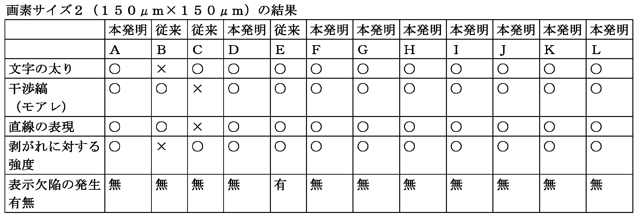
- Each of the information display panels having the cell shape shown in FIGS. 11 (a) to 11 (l) was electrically connected with a driver to display characters. At that time, for each information display panel, investigate the thickness of characters, interference fringes (moire), the expression of straight lines, the strength against peeling, and the presence or absence of display defects. ⁇ , bad ones were evaluated as x. The results are shown in Tables 1 and 2 below.
- the dot matrix type information display panel of the present invention is a notebook computer, electronic notebook, PDA (Personal Digital Assistants), a portable information device called electronic paper used in connection with a mobile device such as a mobile phone, a handy terminal, Electronic paper used as electronic books, electronic newspapers, electronic paper used as bulletin boards such as signboards, posters, blackboards (whiteboards), point cards, IC cards, electronic advertisements, information boards, electronic POPs (Point Of Presence, Point Of Purchase advertising), electronic price tags, electronic shelf labels, RF-ID type electronic paper such as electronic musical scores, POS terminals, car navigation devices, etc.
- a rewritable type that rewrites the display using external rewriting means.
- a child paper suitably used as a child paper.
- the display medium used in the dot matrix type information display panel of the present invention includes a particle group containing conductive particles and a particle group containing semiconductive particles in addition to the particle group containing charged particles described above.
- Various types of particle groups can be used.
- the driving method of the electronic paper of the present invention a simple matrix driving method and a static driving method that do not use a switching element in the panel itself, and a three-terminal switching element represented by a thin film transistor (TFT) or a thin film diode (TFD) are representative.
- TFT thin film transistor
- TFD thin film diode
- various types of driving methods can be applied.
Landscapes
- Physics & Mathematics (AREA)
- General Physics & Mathematics (AREA)
- Engineering & Computer Science (AREA)
- Theoretical Computer Science (AREA)
- Nonlinear Science (AREA)
- Chemical & Material Sciences (AREA)
- Life Sciences & Earth Sciences (AREA)
- Chemical Kinetics & Catalysis (AREA)
- Electrochemistry (AREA)
- Molecular Biology (AREA)
- Health & Medical Sciences (AREA)
- Optics & Photonics (AREA)
- Electrochromic Elements, Electrophoresis, Or Variable Reflection Or Absorption Elements (AREA)
- Devices For Indicating Variable Information By Combining Individual Elements (AREA)
Abstract
Description
この粒子だけで粒子群を構成して表示媒体としたり、その他の粒子と合わせて粒子群を構成して表示媒体としたりして用いられる。
粒子は、その主成分となる樹脂に、必要に応じて、従来と同様に、荷電制御剤、着色剤、無機添加剤等を含ますことができる。以下に、樹脂、荷電制御剤、着色剤、その他添加剤を例示する。
青色着色剤としては、C.I.ピグメントブルー15:3、C.I.ピグメントブルー15、紺青、コバルトブルー、アルカリブルーレーキ、ビクトリアブルーレーキ、フタロシアニンブルー、無金属フタロシアニンブルー、フタロシアニンブルー部分塩素化物、ファーストスカイブルー、インダンスレンブルーBC等がある。
赤色着色剤としては、ベンガラ、カドミウムレッド、鉛丹、硫化水銀、カドミウム、パーマネントレッド4R、リソールレッド、ピラゾロンレッド、ウォッチングレッド、カルシウム塩、レーキレッドD、ブリリアントカーミン6B、エオシンレーキ、ローダミンレーキB、アリザリンレーキ、ブリリアントカーミン3B、C.I.ピグメントレッド2等がある。
緑色着色剤としては、クロムグリーン、酸化クロム、ピグメントグリーンB、C.I.ピグメントグリーン7、マラカイトグリーンレーキ、ファイナルイエローグリーンG等がある。
橙色着色剤としては、赤色黄鉛、モリブデンオレンジ、パーマネントオレンジGTR、ピラゾロンオレンジ、バルカンオレンジ、インダンスレンブリリアントオレンジRK、ベンジジンオレンジG、インダンスレンブリリアントオレンジGK、C.I.ピグメントオレンジ31等がある。
紫色着色剤としては、マンガン紫、ファーストバイオレットB、メチルバイオレットレーキ等がある。
白色着色剤としては、亜鉛華、酸化チタン、アンチモン白、硫化亜鉛等がある。
これらの顔料および無機系添加剤は、単独であるいは複数組み合わせて用いることができる。このうち特に黒色顔料としてカーボンブラックが、白色顔料として酸化チタンが好ましい。
上記着色剤を配合して、所望の色の粒子を作製できる。
Span=(d(0.9)-d(0.1))/d(0.5)
(但し、d(0.5)は粒子の50%がこれより大きく、50%がこれより小さいという粒子径をμmで表した数値、d(0.1)はこれ以下の粒子の比率が10%である粒子径をμmで表した数値、d(0.9)はこれ以下の粒子が90%である粒子径をμmで表した数値である。)
Spanを5以下の範囲に納めることにより、各粒子のサイズが揃い、均一な表示媒体としての移動が可能となる。
ここで、本発明における粒子径および粒子径分布は、体積基準分布から得られたものである。具体的には、Mastersizer2000(Malvern Instruments Ltd.)測定機を用いて、窒素気流中に粒子を投入し、付属の解析ソフト(Mie理論を用いた体積基準分布を基本としたソフト)にて、粒子径および粒子径分布の測定を行なうことができる。
この空隙部分とは、例えば図1(a)、(b)において、対向する基板1、基板2に挟まれる部分から、電極5、6(電極を基板の内側に設けた場合)、表示媒体の占有部分、隔壁4の占有部分、情報表示用パネルのシール部分を除いた、いわゆる表示媒体が接する気体部分を指すものとする。
空隙部分の気体は、先に述べた湿度領域であれば、その種類は問わないが、乾燥空気、乾燥窒素、乾燥アルゴン、乾燥ヘリウム、乾燥二酸化炭素、乾燥メタンなどが好適である。この気体は、その湿度が保持されるように情報表示用パネルに封入することが必要であり、例えば、表示媒体の充填、情報表示用パネルの組み立てなどを所定湿度環境下にて行い、さらに、外からの水分(湿分)侵入を防ぐシール材、シール方法を施すことが肝要である。
対向する基板間の気体中空間における表示媒体の体積占有率は5~70%が好ましく、さらに好ましくは5~60%である。70%を超える場合には表示媒体の移動に支障をきたし、5%未満の場合にはコントラストが不明確となり易い。
・ PETフィルム上に、140μmピッチ、長さ30mmのストライプ形状のライン電極と駆動用ドライバーへの引き回し部分、情報表示用パネル製造時の貼り合わせなどのためのアライメントマークを、ITOのフォトリソグラフィーにより形成した。なお、ライン電極間隔(スペース)は20μmとした。‥‥(画素サイズ2)
・ 隔壁の幅は20μmとした。
・ 黒色表示媒体:平均粒子径9.1μmの正帯電性黒色粒子の粒子群
・ 白色表示媒体:平均粒子径8.8μmの負帯電性黒色粒子の粒子群
・ PETフィルム上に200μmピッチ、長さ30mmのストライプ形状のライン電極とドライバーへの引き回し部分、情報表示用パネル製造時の貼り合わせなどのためのアライメントマークとともに形成した。なお、ライン電極間隔(スペース)は20μmとした。‥‥(画素サイズ1)
・ PETフィルム上に150μmピッチ、長さ30mmのストライプ形状のライン電極とドライバーへの引き回し部分、情報表示用パネル製造時の貼り合わせなどのためのアライメントマークを、ITOのフォトリソグラフィーにより形成した。なお、ライン電極間隔(スペース)は20μmとした。‥‥(画素サイズ2)
・ 隔壁の幅は20μmとした。
・ 隔壁の高さは50μmとした。また、隔壁の頂上にエポキシ系接着剤を配置して、もう一方のPETフィルム基板と貼り合わせた。

Claims (6)
- 少なくとも一方が透明な対向する2枚の基板間に、隔壁によって仕切られた複数のセルを形成し、セル内に粒子群として構成した表示媒体を配置し、基板に形成した四角形画素電極対を用いて表示媒体を電気的に駆動させて、画像等の情報を表示する四角形ドットマトリックス型情報表示用パネルにおいて、
前記複数のセルを、セル形状が少なくとも6辺以上の偶数辺となる多角形セルとし、前記多角形形状を単位とした複数のセルを規則的に配列して表示領域に配置したことを特徴とするドットマトリックス型情報表示用パネル。 - 前記多角形セルの隔壁部分がすべて直角に接続されていることを特徴とする請求項1に記載のドットマトリックス型情報表示用パネル。
- 前記多角形のセル形状が、L型形状、階段形状、凸形状のいずれかであることを特徴とする請求項1または2に記載のドットマトリックス型情報表示用パネル。
- 前記基板に形成した四角形画素電極対サイズが、100μm以上×100μm以上の四角形であることを特徴とする請求項1~3のいずれか1項に記載のドットマトリックス型情報表示用パネル。
- 前記隔壁の幅が、5μm~50μmの範囲であることを特徴とする請求項1~4のいずれか1項に記載のドットマトリックス型情報表示用パネル。
- 前記隔壁を、フォトリソ法で形成したことを特徴とする請求項1~5のいずれか1項に記載のドットマトリックス型情報表示用パネル。
Priority Applications (4)
| Application Number | Priority Date | Filing Date | Title |
|---|---|---|---|
| CN2009801356858A CN102150077A (zh) | 2008-07-24 | 2009-07-24 | 点阵型信息显示面板 |
| US13/055,342 US20110176198A1 (en) | 2008-07-24 | 2009-07-24 | Dot matrix type information display panel |
| JP2010521752A JPWO2010010954A1 (ja) | 2008-07-24 | 2009-07-24 | ドットマトリックス型情報表示用パネル |
| EP09800468A EP2315072A4 (en) | 2008-07-24 | 2009-07-24 | DOT MATRIX INFORMATION SCOREBOARD |
Applications Claiming Priority (2)
| Application Number | Priority Date | Filing Date | Title |
|---|---|---|---|
| JP2008-191388 | 2008-07-24 | ||
| JP2008191388 | 2008-07-24 |
Publications (1)
| Publication Number | Publication Date |
|---|---|
| WO2010010954A1 true WO2010010954A1 (ja) | 2010-01-28 |
Family
ID=41570414
Family Applications (1)
| Application Number | Title | Priority Date | Filing Date |
|---|---|---|---|
| PCT/JP2009/063289 Ceased WO2010010954A1 (ja) | 2008-07-24 | 2009-07-24 | ドットマトリックス型情報表示用パネル |
Country Status (5)
| Country | Link |
|---|---|
| US (1) | US20110176198A1 (ja) |
| EP (1) | EP2315072A4 (ja) |
| JP (1) | JPWO2010010954A1 (ja) |
| CN (1) | CN102150077A (ja) |
| WO (1) | WO2010010954A1 (ja) |
Cited By (1)
| Publication number | Priority date | Publication date | Assignee | Title |
|---|---|---|---|---|
| WO2013122952A1 (en) * | 2012-02-14 | 2013-08-22 | Sipix Imaging, Inc. | Microcup designs for electrophoretic display |
Families Citing this family (1)
| Publication number | Priority date | Publication date | Assignee | Title |
|---|---|---|---|---|
| WO2014033235A2 (en) * | 2012-08-31 | 2014-03-06 | Universität Zürich | Device for placing an object in at least a first and a second orientation or spatial location |
Citations (3)
| Publication number | Priority date | Publication date | Assignee | Title |
|---|---|---|---|---|
| JP2001215537A (ja) | 2000-01-31 | 2001-08-10 | Minolta Co Ltd | 可逆性画像表示媒体 |
| JP2005024868A (ja) * | 2003-07-02 | 2005-01-27 | Fuji Xerox Co Ltd | 画像表示媒体 |
| JP2007164122A (ja) * | 2005-11-21 | 2007-06-28 | Bridgestone Corp | 情報表示用パネル |
Family Cites Families (4)
| Publication number | Priority date | Publication date | Assignee | Title |
|---|---|---|---|---|
| US6181393B1 (en) * | 1997-12-26 | 2001-01-30 | Kabushiki Kaisha Toshiba | Liquid crystal display device and method of manufacturing the same |
| US7471369B2 (en) * | 2001-01-11 | 2008-12-30 | Sipix Imaging, Inc. | Transmissive or reflective liquid crystal display and process for its manufacture |
| JP2008523438A (ja) * | 2004-12-10 | 2008-07-03 | ポリマー、ビジョン、リミテッド | 低減されたモアレ効果を有するディスプレイ |
| EP1785767A1 (en) * | 2005-11-09 | 2007-05-16 | Bridgestone Corporation | Information display panel |
-
2009
- 2009-07-24 WO PCT/JP2009/063289 patent/WO2010010954A1/ja not_active Ceased
- 2009-07-24 CN CN2009801356858A patent/CN102150077A/zh active Pending
- 2009-07-24 US US13/055,342 patent/US20110176198A1/en not_active Abandoned
- 2009-07-24 EP EP09800468A patent/EP2315072A4/en not_active Withdrawn
- 2009-07-24 JP JP2010521752A patent/JPWO2010010954A1/ja active Pending
Patent Citations (3)
| Publication number | Priority date | Publication date | Assignee | Title |
|---|---|---|---|---|
| JP2001215537A (ja) | 2000-01-31 | 2001-08-10 | Minolta Co Ltd | 可逆性画像表示媒体 |
| JP2005024868A (ja) * | 2003-07-02 | 2005-01-27 | Fuji Xerox Co Ltd | 画像表示媒体 |
| JP2007164122A (ja) * | 2005-11-21 | 2007-06-28 | Bridgestone Corp | 情報表示用パネル |
Non-Patent Citations (1)
| Title |
|---|
| See also references of EP2315072A4 |
Cited By (1)
| Publication number | Priority date | Publication date | Assignee | Title |
|---|---|---|---|---|
| WO2013122952A1 (en) * | 2012-02-14 | 2013-08-22 | Sipix Imaging, Inc. | Microcup designs for electrophoretic display |
Also Published As
| Publication number | Publication date |
|---|---|
| JPWO2010010954A1 (ja) | 2012-01-05 |
| EP2315072A1 (en) | 2011-04-27 |
| CN102150077A (zh) | 2011-08-10 |
| US20110176198A1 (en) | 2011-07-21 |
| EP2315072A4 (en) | 2011-11-30 |
Similar Documents
| Publication | Publication Date | Title |
|---|---|---|
| JP5116387B2 (ja) | 情報表示用パネル | |
| JP2008287172A (ja) | 情報表示用パネル | |
| JP5116458B2 (ja) | 情報表示用パネルおよび情報表示用パネルの製造方法 | |
| JP2008299202A (ja) | 情報表示用パネル | |
| JP2008268772A (ja) | 情報表示用パネルの製造方法 | |
| WO2010010954A1 (ja) | ドットマトリックス型情報表示用パネル | |
| JP2009103886A (ja) | 情報表示用パネル | |
| WO2011077668A1 (ja) | 情報表示用パネル及びその製造方法 | |
| JP2007122026A (ja) | 情報表示用パネルおよびその製造方法 | |
| JPWO2009148123A1 (ja) | 情報表示用パネルの駆動方法 | |
| JP2008268771A (ja) | 情報表示用パネルの製造方法 | |
| JP2008224738A (ja) | 情報表示用パネルの活性化方法 | |
| JP5032192B2 (ja) | 情報表示用パネル | |
| JP2010224143A (ja) | ドットマトリックス型情報表示用パネル | |
| JP2007156445A (ja) | 情報表示用パネル | |
| JP5112768B2 (ja) | 情報表示用パネルのマザーパネルおよび情報表示用パネル | |
| JP2009069405A (ja) | 情報表示用パネル | |
| JP2010266837A (ja) | 情報表示用パネル及びその製造方法 | |
| JP2008096495A (ja) | 情報表示装置 | |
| JP2010032724A (ja) | マザー基板、マザー基板に設けた電極の断線検査方法およびマザー基板を用いて作製した情報表示用パネル | |
| JP2007164150A (ja) | 情報表示用パネル | |
| JP2010197731A (ja) | 情報表示用パネル | |
| JP2009151174A (ja) | 情報表示用パネルの製造方法 | |
| JP2008224749A (ja) | 情報表示用パネル | |
| JP2007086475A (ja) | マザー基板構造およびその製造方法 |
Legal Events
| Date | Code | Title | Description |
|---|---|---|---|
| WWE | Wipo information: entry into national phase |
Ref document number: 200980135685.8 Country of ref document: CN |
|
| 121 | Ep: the epo has been informed by wipo that ep was designated in this application |
Ref document number: 09800468 Country of ref document: EP Kind code of ref document: A1 |
|
| WWE | Wipo information: entry into national phase |
Ref document number: 2010521752 Country of ref document: JP |
|
| NENP | Non-entry into the national phase |
Ref country code: DE |
|
| WWE | Wipo information: entry into national phase |
Ref document number: 2009800468 Country of ref document: EP |
|
| WWE | Wipo information: entry into national phase |
Ref document number: 13055342 Country of ref document: US |