WO2010013639A1 - 表示装置および表示装置の製造方法 - Google Patents
表示装置および表示装置の製造方法 Download PDFInfo
- Publication number
- WO2010013639A1 WO2010013639A1 PCT/JP2009/063190 JP2009063190W WO2010013639A1 WO 2010013639 A1 WO2010013639 A1 WO 2010013639A1 JP 2009063190 W JP2009063190 W JP 2009063190W WO 2010013639 A1 WO2010013639 A1 WO 2010013639A1
- Authority
- WO
- WIPO (PCT)
- Prior art keywords
- electrode
- wiring
- organic
- film
- substrate
- Prior art date
- Legal status (The legal status is an assumption and is not a legal conclusion. Google has not performed a legal analysis and makes no representation as to the accuracy of the status listed.)
- Ceased
Links
Images


Classifications
-
- H—ELECTRICITY
- H10—SEMICONDUCTOR DEVICES; ELECTRIC SOLID-STATE DEVICES NOT OTHERWISE PROVIDED FOR
- H10D—INORGANIC ELECTRIC SEMICONDUCTOR DEVICES
- H10D86/00—Integrated devices formed in or on insulating or conducting substrates, e.g. formed in silicon-on-insulator [SOI] substrates or on stainless steel or glass substrates
- H10D86/40—Integrated devices formed in or on insulating or conducting substrates, e.g. formed in silicon-on-insulator [SOI] substrates or on stainless steel or glass substrates characterised by multiple TFTs
-
- H—ELECTRICITY
- H10—SEMICONDUCTOR DEVICES; ELECTRIC SOLID-STATE DEVICES NOT OTHERWISE PROVIDED FOR
- H10D—INORGANIC ELECTRIC SEMICONDUCTOR DEVICES
- H10D30/00—Field-effect transistors [FET]
- H10D30/60—Insulated-gate field-effect transistors [IGFET]
- H10D30/67—Thin-film transistors [TFT]
- H10D30/674—Thin-film transistors [TFT] characterised by the active materials
- H10D30/6755—Oxide semiconductors, e.g. zinc oxide, copper aluminium oxide or cadmium stannate
-
- H—ELECTRICITY
- H10—SEMICONDUCTOR DEVICES; ELECTRIC SOLID-STATE DEVICES NOT OTHERWISE PROVIDED FOR
- H10D—INORGANIC ELECTRIC SEMICONDUCTOR DEVICES
- H10D86/00—Integrated devices formed in or on insulating or conducting substrates, e.g. formed in silicon-on-insulator [SOI] substrates or on stainless steel or glass substrates
- H10D86/40—Integrated devices formed in or on insulating or conducting substrates, e.g. formed in silicon-on-insulator [SOI] substrates or on stainless steel or glass substrates characterised by multiple TFTs
- H10D86/441—Interconnections, e.g. scanning lines
-
- H—ELECTRICITY
- H10—SEMICONDUCTOR DEVICES; ELECTRIC SOLID-STATE DEVICES NOT OTHERWISE PROVIDED FOR
- H10D—INORGANIC ELECTRIC SEMICONDUCTOR DEVICES
- H10D86/00—Integrated devices formed in or on insulating or conducting substrates, e.g. formed in silicon-on-insulator [SOI] substrates or on stainless steel or glass substrates
- H10D86/40—Integrated devices formed in or on insulating or conducting substrates, e.g. formed in silicon-on-insulator [SOI] substrates or on stainless steel or glass substrates characterised by multiple TFTs
- H10D86/60—Integrated devices formed in or on insulating or conducting substrates, e.g. formed in silicon-on-insulator [SOI] substrates or on stainless steel or glass substrates characterised by multiple TFTs wherein the TFTs are in active matrices
-
- H—ELECTRICITY
- H10—SEMICONDUCTOR DEVICES; ELECTRIC SOLID-STATE DEVICES NOT OTHERWISE PROVIDED FOR
- H10K—ORGANIC ELECTRIC SOLID-STATE DEVICES
- H10K50/00—Organic light-emitting devices
- H10K50/80—Constructional details
- H10K50/805—Electrodes
- H10K50/81—Anodes
- H10K50/813—Anodes characterised by their shape
-
- H—ELECTRICITY
- H10—SEMICONDUCTOR DEVICES; ELECTRIC SOLID-STATE DEVICES NOT OTHERWISE PROVIDED FOR
- H10K—ORGANIC ELECTRIC SOLID-STATE DEVICES
- H10K59/00—Integrated devices, or assemblies of multiple devices, comprising at least one organic light-emitting element covered by group H10K50/00
- H10K59/10—OLED displays
- H10K59/12—Active-matrix OLED [AMOLED] displays
- H10K59/125—Active-matrix OLED [AMOLED] displays including organic TFTs [OTFT]
-
- H—ELECTRICITY
- H10—SEMICONDUCTOR DEVICES; ELECTRIC SOLID-STATE DEVICES NOT OTHERWISE PROVIDED FOR
- H10K—ORGANIC ELECTRIC SOLID-STATE DEVICES
- H10K59/00—Integrated devices, or assemblies of multiple devices, comprising at least one organic light-emitting element covered by group H10K50/00
- H10K59/10—OLED displays
- H10K59/12—Active-matrix OLED [AMOLED] displays
- H10K59/131—Interconnections, e.g. wiring lines or terminals
Definitions
- the present invention relates to a display device including a semiconductor element and a light emitting element that emits light according to driving of the semiconductor element, and a method for manufacturing the display device.
- the display device includes a semiconductor element and a light emitting element that emits light in response to driving of the semiconductor element, and displays predetermined image information by controlling light emission of the light emitting element.
- a display device using, for example, an organic electroluminescence (EL) element as a light emitting element has been put into practical use (see, for example, Patent Document 1).
- EL organic electroluminescence
- each pixel includes an organic EL element and a transistor (semiconductor element) that drives the organic EL element.
- an organic EL element is a current drive element that emits light in response to a current supplied from a power supply line. Therefore, in a display device in which a large number of organic EL elements are integrated, It is necessary to pass a very large drive current through a wiring such as a power supply line connecting the EL element and the power supply. If the resistance value of the wiring through which the drive current flows is large, the voltage drop becomes large. Therefore, it is necessary to increase the drive voltage, resulting in a problem that the power consumption of the display device increases. Therefore, conventionally, the resistance value in the current path from the power supply to the organic EL element has been reduced by increasing the width of the wiring connected to the power supply and the electrode in each element, and further increasing the thickness. .
- a light emitting layer of an organic EL element called a top emission type that generally extracts light from the side opposite to a substrate on which a transistor element is formed is formed on the upper surface of a layer in which large unevenness occurs.
- the light emitting layer of the top emission type organic EL element is formed on a layer above the layer on which wirings, electrodes, and the like are formed, using a film forming technique such as a solution coating process or a vacuum deposition method.
- the light emitting layer of the organic EL element is within the same pixel under the influence of the unevenness as compared with the vacuum deposition method. Therefore, the film is formed with a non-uniform film thickness. If the film thickness of the light emitting layer is not uniform, the light emission characteristics of the organic EL element are greatly different due to the influence of the film thickness distribution even within the same pixel. For this reason, there is a problem in that the light emission luminance in the pixels with respect to the same drive current becomes non-uniform, resulting in performance degradation of the display device.
- the present invention has been made in view of the above problems, and suppresses a voltage drop due to wiring resistance, improves the flatness of the element film thickness in the same pixel, and reduces variations in light emission characteristics in the same pixel. It is an object to provide a display device that can be reduced and a method for manufacturing the display device.
- a semiconductor element including a gate electrode, a source electrode, a drain electrode, and a semiconductor film formed between the source electrode and the drain electrode, and a light emitting element including an electrode and electrically connected to the semiconductor element
- the semiconductor element and the light emitting element, and the semiconductor element and the light emitting element are connected to a power source and include a region where the light emitting element is provided when viewed from the thickness direction of the substrate.
- the wiring layer is made of a metal material or an oxide conductive material.
- the semiconductor film is made of an inorganic oxide semiconductor material.
- the semiconductor film is made of an organic semiconductor material.
- a method for manufacturing a display device comprising: an element; and a substrate on which the semiconductor element and the light emitting element are provided, the region being connected to a power source and provided with the light emitting element as viewed in the thickness direction of the substrate
- the gate electrode, the source electrode, and the drain electrode are formed on the flat wiring layer connected to the power source, it is possible to reduce the unevenness of the surface of the layer on which the organic EL element is formed. It can reduce that the light emitting layer of the organic EL element formed on this layer becomes a nonuniform film thickness. Thereby, it is possible to realize a display device and a method for manufacturing the display device that can reduce variations in light emission characteristics in the entire device and in the same pixel, and as a result, can improve performance.
- FIG. 1 is a diagram showing an example of a block diagram of an organic EL display device according to Embodiment 1 of the present invention.
- FIG. 2 is a circuit diagram corresponding to one pixel of the organic EL display device according to the first exemplary embodiment of the present invention.
- FIG. 3 is a diagram showing a cross section of each element constituting one pixel of the organic EL display device according to the first embodiment of the present invention.
- FIG. 4A is a layout diagram of the substrate and the wiring layer shown in FIG.
- FIG. 4B is a conceptual diagram for explaining a schematic path of current in the layout of the wiring layer shown in FIG.
- FIG. 5 is a diagram schematically showing a wiring structure of drive signal lines in a conventional organic EL display device.
- FIG. 1 is a diagram showing an example of a block diagram of an organic EL display device according to Embodiment 1 of the present invention.
- FIG. 2 is a circuit diagram corresponding to one pixel of the organic EL display device according to the first
- FIG. 6 is a cross-sectional view of a pixel driving transistor and an organic EL element in a conventional organic EL display device.
- FIG. 7A is a cross-sectional view illustrating a method of manufacturing the pixel shown in FIG.
- FIG. 7-2 is a cross-sectional view illustrating the method of manufacturing the pixel shown in FIG.
- FIG. 7C is a cross-sectional view illustrating the method of manufacturing the pixel shown in FIG. 7-4 is a cross-sectional view illustrating the method of manufacturing the pixel shown in FIG.
- FIG. 7-5 is a cross-sectional view illustrating the method of manufacturing the pixel shown in FIG. 7-6 is a cross-sectional view illustrating the method of manufacturing the pixel shown in FIG.
- FIG. 7-7 is a cross-sectional view illustrating the method of manufacturing the pixel shown in FIG.
- FIG. 8 is a diagram showing another example of a cross section of each element constituting one pixel of the organic EL display device according to Embodiment 1 of the present invention.
- FIG. 9A is a cross-sectional view illustrating the method of manufacturing the pixel shown in FIG.
- FIG. 9-2 is a cross-sectional view illustrating the method of manufacturing the pixel shown in FIG.
- FIG. 9C is a cross-sectional view illustrating the method of manufacturing the pixel shown in FIG.
- FIG. 9D is a cross-sectional view illustrating the method of manufacturing the pixel shown in FIG. 9-5 is a cross-sectional view illustrating the method of manufacturing the pixel shown in FIG.
- FIG. 9-6 is a cross-sectional view illustrating the method of manufacturing the pixel shown in FIG.
- FIG. 10 is a diagram showing a cross section of each element constituting one pixel of an organic EL display device according to another embodiment of the present invention.
- FIG. 11A is a layout diagram of the substrate and the wiring layer shown in FIG.
- FIG. 11B is a conceptual diagram for explaining a schematic path of current in the layout of the wiring layer shown in FIG. 11A.
- FIG. 12-3 is a cross-sectional view illustrating the method of manufacturing the pixel shown in FIG. 12-4 is a cross-sectional view illustrating the method of manufacturing the pixel shown in FIG. 12-5 is a cross-sectional view illustrating the method of manufacturing the pixel shown in FIG. 12-6 is a cross-sectional view illustrating the method of manufacturing the pixel shown in FIG.
- FIG. 13 is a diagram showing another example of a cross section of each element constituting one pixel of an organic EL display device according to another embodiment of the present invention.
- FIG. 14A is a cross-sectional view illustrating a method of manufacturing the pixel shown in FIG.
- FIG. 14B is a cross-sectional view illustrating the method of manufacturing the pixel shown in FIG. FIG.
- FIG. 14C is a cross-sectional view illustrating the method of manufacturing the pixel shown in FIG. 14-4 is a cross-sectional view illustrating the method of manufacturing the pixel shown in FIG.
- FIG. 14-5 is a cross-sectional view illustrating the method of manufacturing the pixel shown in FIG.
- FIG. 15 is a schematic diagram of the layout of the substrate and the wiring layer applied to the simulation.
- FIG. 1 is a diagram illustrating an example of a block diagram of the organic EL display device according to the first embodiment.
- the organic EL display device according to the first embodiment controls a display panel 603, a scan driver 604, a data driver 605, a drive voltage generator 607, and the display panel 603 connected thereto.
- a signal control unit 606 is included.
- Display panel 603 is connected to the scan driver 604, the scanning signal lines G 1 to transmit a scanning signal Vg, G 2, G 3, ⁇ , is connected to G n, and the data driver 605, the data It is connected to a plurality of signal lines such as data signal lines D 1 , D 2 , D 3 ,..., D m that transmit the signal Vd.
- Each scanning signal line G 1 to G n extends substantially in the row direction, and each data signal line D 1 to D m extends substantially in the column direction.
- the display panel 603 includes a plurality of pixels PX arranged in a matrix so as to be connected to the scanning signal lines G 1 to G n and the data signal lines D 1 to D m , respectively.
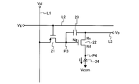
- FIG. 2 is a circuit diagram corresponding to one pixel of the organic EL display device according to the first embodiment.
- the display panel 603 further includes a signal line L ⁇ b> 3 that transmits the drive voltage signal Vp output from the drive voltage generation unit 607.
- the signal line L3 functions as a power supply line that supplies current.
- each pixel includes a switching transistor 21 corresponding to a semiconductor element, a driving transistor 22, a capacitor 23, and an organic EL element 24 corresponding to a light emitting element.
- the signal line L1 shown in FIG. 2 corresponds to the data signal line of this pixel, and the signal line L2 corresponds to the scanning signal line of this pixel.
- the input terminal of the switching transistor 21 is connected to the signal line L1, the control terminal is connected to the signal line L2, and the output terminal is connected to the control terminal Ng of the drive transistor 22.
- the switching transistor 21 outputs the data signal Vd applied to the data line L1 to the drive transistor 22 in response to the scanning signal Vg applied to the signal line L2 that is the scanning signal line.
- the control terminal Ng of the drive transistor 22 is connected to the switching transistor 21, and the output terminal Nd is connected to the organic EL element 24.
- the input terminal Ns of the drive transistor 22 is connected to the signal line L3.
- the drive transistor 22 supplies the organic EL element 24 with an output current I whose magnitude is controlled according to the magnitude of the voltage Vgs applied between the control terminal Ng and the input terminal Ns. This output current I is supplied from the signal line L3 functioning as a power supply line via the input terminal Ns.
- the capacitor 23 is provided between the control terminal Ng of the drive transistor 22 and the input terminal Ns, and charges the data signal Vd applied to the control terminal Ng of the drive transistor 22 and holds it for a certain period.
- the cathode electrode of the organic EL element 24 is connected to the common voltage Vcom, and the anode electrode is connected to the output terminal Nd of the drive transistor 22.
- the organic EL element 24 emits light with luminance corresponding to the output current I by driving the driving transistor 22.
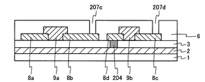
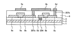
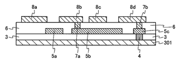
- FIG. 3 is a diagram showing a cross section of each element constituting one pixel of the organic EL display device according to the first embodiment.
- a switching transistor 21, a drive transistor 22, a capacitor 23, and an organic EL element 24 are formed on a substrate 1 such as glass or plastic. Is done.
- the switching transistor 21 is formed between a gate electrode 5a that functions as a control terminal, a source electrode 8a that functions as an input terminal, a drain electrode 8b that functions as an output terminal, and a source electrode 8a and a drain electrode 8b. And a semiconductor film 9a functioning as Gate electrode 5a is connected to signal line L2 in a region not shown, and source electrode 8a is connected to signal line L1 in a region not shown.
- a gate insulating film 6 is formed between the gate electrode 5a and the source electrode 8a, the drain electrode 8b, and the semiconductor film 9a.
- the drive transistor 22 is formed between the gate electrode 5b functioning as the control terminal Ng, the source electrode 8d functioning as the input terminal Ns, the drain electrode 8c functioning as the output terminal Nd, and the source electrode 8d and the drain electrode 8c. And a semiconductor film 9b functioning as a channel layer.
- the gate electrode 5b is connected to the drain electrode 8b of the switching transistor 21 through the in-contact wiring 7a.
- a gate insulating film 6 is formed between the gate electrode 5b and the source electrode 8d, the drain electrode 8c, and the semiconductor film 9b.
- the contact wiring 7a includes gate electrodes 5a and 5b (first gate electrode 5a and second gate electrode 5b), source electrodes 8a and 8d (first source electrode 8a and second source electrode 8b), and drain electrode 8b. , 8c (first drain electrode 8a, second drain electrode 8c).
- the in-contact wiring 7a corresponds to the point P3 shown in FIG.
- the organic EL element 24 is formed on the anode electrode 12 connected to the drain electrode 8 c of the driving transistor 22 via the contact wiring 11, the organic film 13 formed on the anode electrode 12, and the organic film 13. And a cathode electrode 14. Furthermore, the organic film 13 includes at least an organic light emitting layer, and emits light with luminance according to the amount of current supplied from the anode electrode 12. In addition, you may provide a positive hole injection layer, a positive hole transport layer, an electron carrying layer, an electron injection layer, a positive hole barrier layer, etc. between the anode electrode 12 and the cathode electrode 14 as needed.
- the in-contact wiring 11 is formed between the source electrodes 8a and 8d, the drain electrodes 8b and 8c, the semiconductor films 9a and 9b (first semiconductor film 9a and second semiconductor film 9b), and the anode electrode 12 of the organic EL element 24. It is provided on the formed interlayer insulating film 10.
- the interlayer insulating film 10 includes, for example, a semiconductor protective film that protects a semiconductor of a transistor and a planarization film that is formed for planarization.
- An interlayer film 15 having an opening provided only in a region where the organic EL element 24 is formed is laminated between the interlayer insulating film 10 and the cathode electrode 14.
- the in-contact wiring 11 corresponds to the point P4 shown in FIG.
- the cathode electrode 14 is formed of a transparent film or a semi-transparent film.
- a protective film 16 formed of a transparent film or a semi-transparent film and an upper substrate 17 that is transparent or semi-transparent are provided.
- Light emitted from the organic film 13 sequentially passes through the cathode electrode 14, the protective film 16, and the upper substrate 17 and is output to the outside. Therefore, the organic EL element 24 is a so-called top emission type.
- a wiring layer 2 is formed immediately above the substrate 1. That is, the wiring layer 2 is provided between the switching transistor 21, the driving transistor 22 and the organic EL element 24 and the substrate 1.
- the wiring layer 2 is made of a conductive material and is connected to a power source.
- a contact hole is formed in the wiring layer 2, and an in-contact wiring is formed in the contact hole.
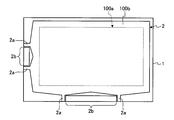
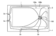
- the wiring layer 2 is a region in which the organic EL elements 24 are arranged in a matrix when viewed from the thickness direction of the substrate 1 (display this).
- the display area 100a overlaps with the display area 100a in a state in which the area 100a is included.
- the area of the wiring layer 2 viewed from the thickness direction is larger than the area of the display region 100a viewed from the thickness direction.
- the wiring layer 2 extends from the entire periphery of the region (display region 100 a) where the light emitting element (organic EL element 24 in the present embodiment) is provided to the outside of the region (display region 100 a).
- a protruding area 100b is provided. Therefore, the protruding region 100b that protrudes from the overlapping region exists outside the region overlapping the display region 100a in the wiring layer 2.
- the display region 100a is, for example, a region surrounded by connecting at least the outer sides of the organic EL elements 24 arranged on the outermost periphery, and is a region that expresses an image as a whole.
- the current i flowing into the wiring layer 2 from the power supply terminal 2a provided at the end of the substrate 1 flows into the protruding region 100b portion in the wiring layer 2. After that, it is configured to flow into each pixel 100 arranged in the display area 100a from four directions.
- the protruding region 100b that does not overlap with the display region 100a in the thickness direction of the substrate 1 functions as the main wiring portion of the power supply line, and in the present embodiment, it occurs in the wiring layer 2 constituting the power supply line. Voltage drop can be suppressed. As a result, the display quality of the organic EL display device can be improved and the power supply margin can be reduced, so that power consumption can be reduced.
- the wiring layer 2 is formed immediately above the upper surface, which is a flat element forming surface, on the substrate 1, it is formed with a substantially uniform film thickness, and even if the film thickness is increased, there is almost no influence on the upper layer. .
- the wiring layer 2 is formed in, for example, a cutting region on the periphery of the substrate 1 and a region excluding the sealing region and the terminal portion, that is, a region inside the outer edge of the substrate 1.
- the power supply terminal 2a for electrically connecting the wiring layer 2 and the power supply has, for example, four sides forming the outer end of the substrate 1.
- the other electrode terminals 2b can be disposed on at least one side of the two.
- the wiring layer 2 corresponds to the signal line L3 connected to the drive voltage generation unit 607 functioning as a power source. That is, the wiring layer 2 is connected to a power source and supplies current to the organic EL element 24 via the drive transistor 22.
- the wiring layer 2 is a connection film formed in the same layer as the in-contact wiring 4 and the gate electrodes 5 a and 5 b formed in the interlayer insulating film 3 immediately above the wiring layer 2, and is formed immediately above the in-contact wiring 4.
- the connection film 5c is connected to the source electrode 8d of the drive transistor 22 through the contact wiring 7b in the gate insulating film 6 formed immediately above the connection film 5c.
- a current is supplied to the anode electrode 12 of the organic EL element 24.
- the capacitor 23 is formed by a partial region of the wiring layer 2, a partial region of the gate electrode 5b, and a partial region of the interlayer insulating film 3.
- FIG. 5 is a diagram schematically showing a wiring structure of drive signal lines in a conventional organic EL display device
- FIG. 6 is a cross-sectional view of a pixel drive transistor and an organic EL element in the conventional organic EL display device. is there.
- the drive signal line is formed in the same layer as the scanning signal line or the data signal line.
- the display panel 603 The frame-shaped main wiring Lvm arranged so as to surround the display region K2 in FIG. 1 and a portion extending in the row direction in the main wiring Lvm extend in the column direction and branch to transmit a driving voltage signal to each pixel.
- the power supply terminal Ta for electrically connecting the main wiring Lvm and a power supply is, for example, on at least one side of the four sides forming the outer end of the substrate K1, together with other electrode terminals Tb. Can be arranged.
- the input terminal of the drive transistor of each pixel is connected to each branch line Lvb connected to the main line Lvm.
- the organic EL element is a current driving element that emits light according to a current supplied from a power supply line
- a power supply line that supplies current to the organic EL element in a light emitting device in which a large number of organic EL elements are integrated, a power supply line that supplies current to the organic EL element. Therefore, it is necessary to pass a very large current. For this reason, although it is desired to increase the area of the power supply line pattern in order to reduce the resistance of the branch wiring Lvb constituting the power supply line, the space that can be used for the power supply line pattern is limited. For this reason, in the conventional configuration, as shown in FIG.
- the film thickness T108 of the source electrode 108d of the driving transistor is set to about 1 ⁇ m, for example.
- the wiring and the electrode become thicker, resulting in large irregularities in the upper layer of the wiring and the electrode.
- the organic film constituting the organic EL element is applied on the film having large unevenness due to the thickening of the wiring and electrodes, so the organic film of the organic EL element is not uniform due to the influence of the unevenness of the base film. It will be applied with a thick film thickness. As a result, characteristic deterioration due to non-uniformity of light emission luminance occurs.
- the interlayer insulating film 110 formed on the wiring and the electrode very thick.
- the unevenness is absorbed by forming the interlayer insulating film 110 with a very thick film thickness T110 of 5 to 10 ⁇ m.
- the depth of the contact hole formed in the interlayer insulating film 110 becomes deep. In the case where the depth is shallow, the in-contact wiring 111 can be formed together with the electrode in the same step as the step of forming the anode electrode 12.
- the drain electrode 108c of the driving transistor is formed.
- a step of embedding a wiring material in the contact hole is necessary in order to form the in-contact wiring 111 that appropriately connects the anode electrode 12 of the organic EL element 24 .
- the wiring layer 2 is formed immediately above the substrate 1 so as to cover at least the entire display region 100a where the organic EL element 24 is formed. Can be ensured to the maximum. Therefore, in the first embodiment, since the resistance of the wiring layer 2 connected to the power supply line can be sufficiently reduced without increasing the thickness of each electrode, as shown in FIG. Even when the source electrode 8d is formed with a film thickness T8 smaller than the film thickness T108 (see FIG. 6), current supply to the organic EL element 24 can be smoothly performed.
- the thickness of the source electrode and the drain electrode in this embodiment is about 30 nm to 500 nm.
- the source and drain electrodes are Cr, Au, Pt, Pd, APC (Ag—Pd—Cu), Mo, MoO 3 , PEDOT, ITO (indium tin oxide), Ag, Cu, Al, Ti, Ni, It is comprised by Ir, Fe, W, MoW, and the alloy of these, and these laminated films, Preferably it is comprised by the laminated film of Mo, Mo / Al / Mo, Ta / Cu / Ta.
- the wiring layer 2 is formed immediately above the upper surface, which is a flat element formation surface, on the substrate 1, it is formed with a substantially uniform film thickness.
- the voltage drop can be reduced as compared with the conventional linear wiring. Therefore, in the first embodiment, as described above, it is thinner than the conventional one.
- the source electrode 8d can be formed with a film thickness. For this reason, in the first embodiment, as shown in FIG. 3, even when the film thickness T10 is smaller than the conventional film thickness T110 (see FIG. 6), it is formed on the wiring and the electrodes.
- the interlayer insulating film 10 can have a surface that is the same as or more flat than the conventional one.
- the organic film 13 of the organic EL element 24 formed on the interlayer insulating film 10 can be applied with a more uniform film thickness. Therefore, in the first embodiment, it is possible to reduce the formation of the organic film of the organic EL element 24 with a non-uniform film thickness, and to realize more uniform light emission luminance in the entire device and in the same pixel. Furthermore, in the first embodiment, since the interlayer insulating film 10 is thinner than the conventional film, the contact hole in which the contact wiring 11 provided in the interlayer insulating film 10 is formed can be accurately opened by a wet process. Connection failure between the drain electrode 8c of the drive transistor 22 and the anode electrode 12 of the organic EL element 24 can also be prevented.
- the wiring layer 2 and the source electrode 8 d of the driving transistor 22 are interposed between the wiring layer 2 and the source electrode 8 d.
- the wiring layer 2 and the source electrode 8d of the drive transistor 22 can be appropriately connected by providing an in-contact wiring or a connection layer as necessary.
- each branch wiring Lvb branched from the main wiring Lvm shown in FIG. 5 is formed in a line pattern, a voltage drop due to wiring resistance may occur. Therefore, in the conventional configuration, there is a case where a large fluctuation occurs in the voltage applied to the organic EL element 24 in proportion to the current consumption. Therefore, in order to correct the luminance fluctuation due to the voltage fluctuation, the voltage drop Since the voltage added with the fluctuation due to is applied to the main wiring Lvm as the power supply voltage to compensate the drain-source voltage, it is difficult to suppress the power consumption of the entire display device.
- the wiring layer 2 connected to the power source is formed so as to overlap and protrude at least the display region 100a where the organic EL element 24 is formed on the upper surface of the substrate 1.
- the power supply voltage drop is smaller than before. Therefore, in the first embodiment, since the voltage value itself added to the power supply voltage as the fluctuation due to the voltage drop can be made smaller than before, it is possible to reduce the power consumption of the entire display device than before. .
- a sheet member for heat diffusion is separately attached to the display panel, and the display panel generates the heat. The heat was diffusing.
- heat is diffused throughout the display panel via the wiring layer 2. Therefore, when combined with a sheet member for heat diffusion, a higher heat diffusion effect and heat dissipation effect can be expected, so that deterioration of the constituent materials of each pixel can be suppressed and long-term reliability of the display device can be improved.
- the wiring layer 2 is formed in a planar shape (flat plate shape) immediately above the substrate 1, so that the branch wiring Lvb itself becomes unnecessary, and a wiring area for forming this branch wiring Lvb is also secured. Therefore, the aperture ratio can be increased by this wiring area. Further, in the first embodiment, since the branch wiring Lvb itself is not necessary, higher definition can be achieved. Furthermore, in the first embodiment, since one electrode of the capacitor 23 is constituted by a part of the planar wiring layer 2 formed on the substrate 1, the other electrode of the capacitor 23 is the wiring layer. 2 can be formed in any region as long as it is on the interlayer insulating film 3 above. Therefore, in the first embodiment, it is possible to flexibly select the formation region of the capacitor 23.
- FIG. 15 is a schematic diagram of the layout of the substrate and wiring layers applied to the simulation.
- model (I) is a conventional wiring layer including the striped branch wiring described with reference to FIG.
- the model (II) is a wiring layer having a flat plate shape and no protruding region.
- the model (III) is a wiring layer 2 that has a flat plate shape and has a protruding region 100b.
- the sheet resistance is assumed to be 0.065 ⁇ / ⁇ .
- the width W in the direction orthogonal to the extending direction of the protruding region was 462 ⁇ m.
- a balanced bridge circuit that spreads in a mesh pattern over the entire wiring layer was adopted. By configuring the balanced bridge circuit, it is possible to simulate a flat wiring layer having a two-dimensional extension.
- a series resistor is adopted as an equivalent circuit of the branch wiring Lvb of the conventional wiring layer described with reference to FIG.
- the adjacent branch wirings Lvb are electrically connected via the main wiring Lvm (see FIG. 5).
- Resistance is employed as an equivalent circuit of the main wiring Lvm of the conventional wiring layer, and the resistance as the main wiring Lvm is disposed between one end and the other end of the adjacent branch wiring Lvb.
- the display area 100a has a rectangular shape with a diagonal length of 40 inches, and 25 (5 rows ⁇ 5 columns) transistors are arranged in the display area 100a in a grid pattern (not shown).
- the power supply terminal 2c for supplying electric power to the flat wiring layer was disposed in the vicinity of one corner of the four corners of the rectangular wiring layer.
- a simulation was performed on the operation when a voltage of 10 V was applied to the power supply terminal 2c.
- the voltage was calculated for each of the five monitor regions (first monitor region 2d1, second monitor region 2d2, third monitor region 2d3, fourth monitor region 2d4, and fifth monitor region 2d5).
- the first to fifth monitor regions 2d1 to 2d5 are shown as regions surrounded by broken lines, respectively. The results are shown in Table 1.
- the luminance of the light-emitting element is determined by the amount of current flowing through the light-emitting element, and this amount of current greatly depends on the voltage between the gate and source electrodes of the transistor that drives the light-emitting element (sometimes referred to as Vgs).
- Vgs the voltage between the gate and source electrodes of the transistor that drives the light-emitting element
- the voltage applied to the source electrode of the transistor varies depending on the position where the transistor is arranged due to the voltage drop generated in the wiring layer. As a result, the voltage drop generated in the wiring layer emits light. It affects the brightness of the device.
- the Vgs difference between the grayscales is very small, so it is necessary to control Vgs with high precision. If the voltages applied to the electrodes are different, it becomes difficult to control Vgs with high accuracy.
- the voltage drop that occurs in the wiring layer during driving can be suppressed, and the voltage applied to the source electrode of each transistor can be made substantially constant.
- a circuit capable of expressing multi-tone luminance with a low driving voltage can be realized relatively easily.
- the width of the protruding region is preferably 1 ⁇ m or more, and more preferably 50 ⁇ m or more. There is no upper limit to the width of the protruding area, but it is set within a range allowed from the viewpoint of miniaturization.
- the film thickness of the protruding area of the wiring layer is larger than the film thickness of the display area (area where the light emitting element is provided) of the wiring layer.
- 7-1 to 7-7 are cross-sectional views illustrating a method of manufacturing the pixel 100 shown in FIG.
- the wiring layer 2 is formed on the substrate.
- the substrate 1 may be an insulating substrate such as glass or plastic.
- the substrate 1 may be a so-called flexible substrate that is flexible and can be greatly deformed. Further, since the pixel 100 is a top emission type, the substrate 1 is not necessarily transparent.
- the wiring layer 2 is formed of a highly conductive material such as a metal material such as Cr, Ag, Au, Ti, Mo, AL, or Cu, or a transparent oxide conductive material such as ITO or IZO.
- the wiring layer 2 is formed using a method according to a material such as a vacuum deposition method, a sputtering method, a coating method, a printing method, a mask deposition method, an ink jet printing method, and a photolithography method (in this specification,
- the “photolithography method” may include a patterning process such as an etching process) to form a wiring pattern.
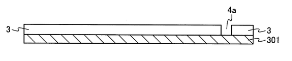
- an interlayer insulating film 3 having a thickness of about 500 nm to 2 ⁇ m is formed immediately above the wiring layer 2.
- Interlayer insulating film 3 for example, spin-on-glass (SOG), photoresist, polyimide, SiNx, is formed by a SiO 2, spin coating, is formed by a sputtering method, and CVD (Chemical vapor deposition) method.
- a contact hole 4a is formed at a position corresponding to the connection film 5c by photolithography. At this time, a contact hole between the electrode terminal 2b and another signal line at the end of the substrate 1 may be formed.
- an in-contact wiring 4 is formed by embedding a conductive material in the contact hole 4a.
- a metal material, a transparent oxide conductive material, or the like is deposited on the interlayer insulating film 3 and the contact wiring 4 using a vacuum deposition method, a sputtering method, or a coating method.
- the gate electrodes 5a and 5b and the connection film 5c are patterned using a photolithography method.
- the entire surface of the contact hole 4a and the gate electrodes 5a and 5b and the connection film 5c are formed using a metal material or a transparent oxide conductive material.
- the contact inner wiring 4, the gate electrodes 5a and 5b, and the connection film 5c may be collectively formed by patterning by photolithography.
- the in-contact wiring 4, the gate electrodes 5a and 5b, and the connection film 5c may be formed using an inkjet printing method, a printing method, or the like. In this step, it is also preferable to form an in-contact wiring for connecting the electrode terminal 2b at the end portion of the substrate 1 and other signal lines.
- a gate insulating film 6 is formed using an organic photosensitive resin or the like as a material.
- the gate insulating film 6 preferably has a dielectric constant of 1.5 or more and a film thickness of 500 nm or less in order to ensure the driving capability of each transistor.
- the gate insulating film 6 is formed using a method according to the material such as a coating method.
- contact holes 7c and 7d are formed in the gate insulating film 6 by using a photolithography method or the like.
- the contact wirings 7a and 7b (first contact wiring 7a and second contact wiring 7b) shown in FIG. 7-5 are formed.
- a metal material, a transparent oxide conductive material, or the like is formed on the entire surface by using a vacuum deposition method, a sputtering method, a coating method, or the like, and then a photolithography method.
- the source electrodes 8a and 8d and the drain electrodes 8b and 8c are patterned using, for example.
- the metal material or the transparent oxide conductive material can be directly used in the contact holes 7c and 7d and the source electrode 8a and 8d and drain electrode 8b and 8c formation regions by using the above method.
- the in-contact wirings 7a and 7b, the source electrodes 8a and 8d, and the drain electrodes 8b and 8c may be formed in a lump by forming a material or the like on the entire surface and then patterning by photolithography.
- the in-contact wirings 7a and 7b, the source electrodes 8a and 8d, and the drain electrodes 8b and 8c may be formed using an inkjet printing method, a printing method, or the like.
- semiconductor films 9a and 9b are formed between the source electrodes 8a and 8d and the drain electrodes 8b and 8c.
- the semiconductor films 9a and 9b are made of an inorganic oxide semiconductor material such as ZTO, an organic semiconductor material having a precursor of pentacene or tetrabenzoporphyrin, or an inorganic semiconductor material such as amorphous silicon and polysilicon.
- the semiconductor films 9a and 9b are formed using a method according to the material such as a vacuum deposition method, a sputtering method, a coating method or a CVD method, and then patterned using a photolithography method.
- the semiconductor films 9a and 9c may be formed using an ink jet printing method, a printing method, or the like.
- a protective film (not shown) is formed on the semiconductor films 9a and 9b, the planarization function is performed to absorb the unevenness of the source electrodes 8a and 8d, the drain electrodes 8b and 8c, and the semiconductor films 9a and 9b.
- An interlayer insulating film 10 having the following is formed.
- This interlayer insulating film 10 is formed of, for example, a photosensitive resin and has a thickness of about 2 ⁇ m to 10 ⁇ m.
- a contact hole 11a is formed in the interlayer insulating film 10 by using a photolithography method.
- the protective film (not shown) preferably has a dielectric constant of 3.5 or less in order to prevent a back channel formed by electrical coupling with the upper electrode, and does not affect the semiconductor characteristics. There must be.
- a conductive material is embedded in the contact hole 11a to form the in-contact wiring 11.
- a metal material, a transparent oxide conductive material, or the like is formed on the entire surface using a vacuum deposition method, a sputtering method, or the like, and then the anode electrode is used using a photolithography method or the like. 12 is patterned.
- the anode electrode 12 is formed of, for example, a laminated film of ITO / Ag / ITO or ITO / Al / ITO.
- a metal material, a transparent oxide conductive material, or the like is formed on the entire surface directly in the contact hole 11a and the anode electrode 12 formation region using the above-described method.
- the in-contact wiring 11 and the anode electrode 12 may be collectively formed by patterning using a lithography method.
- the cathode electrode 14 is formed of a transparent or translucent metal material or an oxide conductive material.
- the cathode electrode 14 is formed of, for example, an alloy material of Mg and Ag.
- the upper substrate 17 is provided on the protective film 16, whereby the pixel 100 shown in FIG. 3 can be obtained.
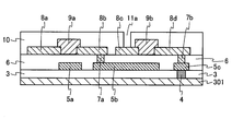
- the pixel 100 having the bottom gate structure in which the gate electrode is formed on the substrate side below the source electrode and the drain electrode has been described as an example.
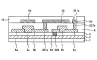
- the pixel 200 may have a top gate structure in which the gate electrodes 5a and 5b are formed on the organic EL element 24 side above the source electrodes 8a and 8d and the drain electrodes 8b and 8c. .
- the pixel 200 includes a switching transistor 21 having a gate electrode 5a, a source electrode 8a, a drain electrode 8b, and a semiconductor film 9a, a gate electrode 5b, a source electrode 8d, and a drain electrode 8c, as in the pixel 100.
- a driving transistor 22 having a semiconductor film 9b, and an organic EL element 24 having an anode electrode 12, an organic film 13, and a cathode electrode 14.
- a gate insulating film 6 is formed between the source electrodes 8a and 8d, the drain electrodes 8b and 8c, the semiconductor films 9a and 9b, and the gate electrodes 5a and 5b.
- the pixel 200 has a top gate structure in which the gate electrodes 5a and 5b are formed on the organic EL element 24 side above the source electrodes 8a and 8d and the drain electrodes 8b and 8c.
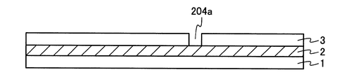
- the pixel 200 has a wiring layer 2 formed immediately above the substrate 1, as in the pixel 100.
- the wiring layer 2 is connected to the source electrode 8 d of the drive transistor 22 through the contact wiring 204 formed in the interlayer insulating film 3.
- the drain electrode 8c of the drive transistor 22 is a connection film formed in the same layer as the in-contact wiring 207b and the gate electrodes 5a and 5b formed in the gate insulating film 6 and formed immediately above the in-contact wiring 207b.
- the anode 5 is connected to the anode electrode 12 of the organic EL element 24 via the in-contact wiring 211 in the interlayer insulating film 10 formed immediately above the film 5d and the connection film 5d.
- the gate electrode 5 b of the drive transistor 22 is connected to the drain electrode 8 b of the switching transistor 21 through the contact wiring 207 a formed in the gate insulating film 6.
- the capacitor 23 is formed by a partial region of the wiring layer 2, a partial region of the drain electrode 8b, and a partial region of the interlayer insulating film 3.
- the thickness of each electrode is not increased.
- the resistance of the wiring layer 2 functioning as a power supply line can be sufficiently reduced, and the surface of the interlayer insulating film 10 is not generated due to the wiring layer 2 and is flat and more uniform. Since the organic film 13 having a film thickness can be formed, it is possible to achieve the same effect as the pixel 100 in that it is possible to achieve uniform emission luminance throughout the device and in the same pixel, as well as to reduce power consumption and prevent heat concentration. It becomes possible.
- FIGS. 9-1 to 9-6 are cross-sectional views showing a method for manufacturing the pixel 200 shown in FIG.
- the wiring layer 2 is formed similarly to the case shown in FIG.
- FIG. 9B after the interlayer insulating film 3 is formed immediately above the wiring layer 2, a contact hole 204a is formed at a position corresponding to the source electrode 8d by photolithography. Then, as shown in FIG.
- the source electrodes 8a and 8d and the drain electrodes 8b After forming the in-contact wiring 204 by embedding a conductive material in the contact hole 204a, the source electrodes 8a and 8d and the drain electrodes 8b, In order to form 8c, a metal material, a transparent oxide conductive material, or the like is formed using a vacuum deposition method, a sputtering method, a coating method, or the like, and the source electrodes 8a and 8d and the drain electrodes 8b and 8c are used using a photolithography method or the like. Is patterned.
- the in-contact wiring 204, the source electrodes 8a and 8d, and the drain electrodes 8b and 8c can be formed in a lump.
- semiconductor films 9a and 9b are formed between the source electrodes 8a and 8d and the drain electrodes 8b and 8c.
- a gate insulating film 6 is formed in the same manner as described above.
- a conductive material is formed in the contact holes 207c and 207d.
- the contact wirings 207a and 207b are formed.
- a metal material, a transparent oxide conductive material, or the like is applied to the gate insulating film by using a vacuum deposition method, a sputtering method, or a coating method in order to form the gate electrodes 5a and 5b and the connection film 5d.
- a vacuum deposition method, a sputtering method, or a coating method in order to form the gate electrodes 5a and 5b and the connection film 5d.
- the gate electrodes 5a and 5b and the connection film 5d are patterned by using a photolithography method.
- the in-contact wirings 207a and 207b, the gate electrodes 5a and 5b, and the connection film 5d can be collectively formed.
- the contact hole 211a is formed in the interlayer insulating film 10. .
- the contact wiring 211 is formed by embedding a conductive material in the contact hole 211a, the anode electrode 12 of the organic EL element 24 is formed, and then the organic film of the organic EL element 24 is formed. Is applied onto the anode electrode 12.
- the cathode electrode 14 is formed, the protective film 16 for protecting the organic EL element 24 is formed, and then the upper substrate 17 is provided on the protective film 16, as shown in FIG. Pixel 200 can be obtained.
- each electrode of each transistor may be formed of a transparent electrode, and a wiring layer connected to the source electrode of the driving transistor may be formed on a transparent substrate using a transparent conductive material.
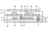
- FIG. 10 is a diagram showing a cross section of each element constituting one pixel of the organic EL display device according to the present embodiment.
- the organic EL display device according to the present embodiment has the device configuration shown in FIG. 1 as in the first embodiment, and each pixel has the circuit configuration shown in FIG.
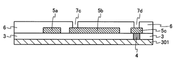
- the pixel 300 of the organic EL display device according to the present embodiment includes a switching transistor 21, a drive transistor 22, a capacitor 23, and an organic EL element 24.
- the pixel 300 has high conductivity and is formed over a metal substrate 301 that functions as a power supply line. Note that part of the metal substrate 301 may function as part of the pixel 300 in some cases.
- the switching transistor 21 is formed between a gate electrode 5a that functions as a control terminal, a source electrode 8a that functions as an input terminal, a drain electrode 8b that functions as an output terminal, and a source electrode 8a and a drain electrode 8b. And a semiconductor film 9a functioning as Gate electrode 5a is connected to signal line L2 in a region not shown, and source electrode 8a is connected to signal line L1 in a region not shown.
- a gate insulating film 6 is formed between the gate electrode 5a and the source electrode 8a, the drain electrode 8b, and the semiconductor film 9a.
- the drive transistor 22 is formed between the gate electrode 5b functioning as the control terminal Ng, the source electrode 8d functioning as the input terminal Ns, the drain electrode 8c functioning as the output terminal Nd, and the source electrode 8d and the drain electrode 8c. And a semiconductor film 9b functioning as a channel layer.
- the gate electrode 5b is connected to the drain electrode 8b of the switching transistor 21 via the in-contact wiring 7a.
- a gate insulating film 6 is formed between the gate electrode 5b and the source electrode 8d, the drain electrode 8c, and the semiconductor film 9b.
- the in-contact wiring 7a is provided in the gate insulating film 6 between the gate electrodes 5a and 5b and the source electrodes 8a and 8d and the drain electrodes 8b and 8c.
- the in-contact wiring 7a corresponds to the point P3 shown in FIG.
- the organic EL element 24 is formed on the anode electrode 12 connected to the drain electrode 8 c of the driving transistor 22 via the contact wiring 11, the organic film 13 formed on the anode electrode 12, and the organic film 13. And a cathode electrode 14. Furthermore, the organic film 13 includes at least an organic light emitting layer, and emits light with luminance according to the amount of current supplied from the anode electrode 12. In addition, you may provide a positive hole injection layer, a positive hole transport layer, an electron carrying layer, an electron injection layer, a positive hole barrier layer, etc. between the anode electrode 12 and the cathode electrode 14 as needed.
- the in-contact wiring 11 is provided in the interlayer insulating film 10 formed between the source electrodes 8a and 8d, the drain electrodes 8b and 8c, the semiconductor films 9a and 9b, and the anode electrode 12 of the organic EL element 24.
- the interlayer insulating film 10 includes, for example, a semiconductor protective film that protects a semiconductor layer of a transistor and a planarization film that is formed for planarization.
- An interlayer film 15 having an opening provided only in a region where the organic EL element 24 is formed is laminated between the interlayer insulating film 10 and the cathode electrode 14.
- the in-contact wiring 11 corresponds to the point P4 shown in FIG.
- the cathode electrode 14 is formed of a transparent film or a semi-transparent film.
- a protective film 16 formed of a transparent film or a semi-transparent film and an upper substrate 17 that is transparent or semi-transparent are provided.
- Light emitted from the organic film 13 sequentially passes through the cathode electrode 14, the protective film 16, and the upper substrate 17 and is output to the outside. Therefore, the organic EL element 24 is a so-called top emission type.
- the switching transistor 21 and the drive transistor 22 as semiconductor elements and the organic EL element 24 as a light emitting element are, for example, one main surface side (for example, the upper surface side) which is an element formation surface of the metal substrate 301.
- the metal substrate 301 corresponds to the signal line L3 connected to the drive voltage generation unit 607 (see FIG. 1) that functions as a power source. That is, the metal substrate 301 functions as a power supply line connected to a power supply, and supplies current to the organic EL element 24 via the drive transistor 22.
- the metal substrate 301 is provided with an interlayer insulating film 3 in which contact holes are formed.
- the metal substrate 301 is a connection film formed in the same layer as the in-contact wiring 4 and the gate electrodes 5 a and 5 b formed in the contact hole of the interlayer insulating film 3, and the connection formed immediately above the in-contact wiring 4.
- the organic EL element is connected to the source electrode 8d of the drive transistor 22 via the contact wiring 7b in the gate insulating film 6 formed immediately above the film 5c and the connection film 5c.
- a current is supplied to the 24 anode electrodes 12.
- the capacitor 23 is formed by a partial region of the metal substrate 301, a partial region of the gate electrode 5b, and a partial region of the interlayer insulating film 3.
- the metal substrate 301 includes a region 300a in which the organic EL elements 24 are arranged in a matrix as viewed from the thickness direction of the metal substrate 301 (this is a display region). It exists so as to overlap in a state of inclusion. Therefore, the protruding region 300b that protrudes from the overlapping region exists outside the overlapping region of the metal substrate 301 with the display region 300a.
- the current i flowing into the metal substrate 301 from the power supply terminal 301a provided at the end of the metal substrate 301 flows into the protruding region 300b in the metal substrate 301.
- the metal substrate 301 is insulated by an insulating film 318 formed so as to cover the vicinity of the four sides of the metal substrate 301 and to cover the surface opposite to the element forming surface. Is done.
- the power supply terminal 301a for connecting the metal substrate 301 to the power supply is disposed, for example, on the insulating film 318 covering the outer edge of the metal substrate 301 together with other electrode terminals 301b. Furthermore, the metal substrate 301 and the power supply terminal 301 a are electrically connected by, for example, a contact plug 301 c that penetrates the insulating film 318.
- the metal substrate 301 itself is used as part of the wiring as the power supply line, so that the area of the power supply line pattern can be ensured to the maximum. Therefore, in this embodiment, since the resistance of the metal substrate 301 that is a part of the power supply line can be sufficiently reduced without increasing the thickness of each electrode, as shown in FIG. Even when the source electrode 8d is formed with a thickness T8 (similar to FIG. 3) smaller than the thickness T108 (see FIG. 6), the current can be smoothly supplied to the organic EL element 24.
- the thickness of the source electrode and the drain electrode in this embodiment is about 30 nm to 500 nm.
- the source and drain electrodes are Cr, Au, Pt, Pd, APC (Ag—Pd—Cu), Mo, MoO 3 , PEDOT, ITO (indium tin oxide), Ag, Cu, Al, Ti, Ni, It is comprised by Ir, Fe, W, MoW, and the alloy of these metals, these laminated films, etc., Preferably it is comprised by Mo, Ta / Cu / Ta, Mo / Al / Mo.
- the metal substrate 301 itself is used as part of the wiring as the power supply line, it is not necessary to separately form a wiring layer as the power supply line. Thereby, the thickness of the display panel can be further reduced. As a result, the organic EL display device can be further reduced in thickness.
- the upper surface which is an element formation surface in the metal substrate 301 is flat.
- the voltage drop can be reduced as compared with the conventional linear wiring. Therefore, as described above, in the present embodiment, a film thinner than the conventional one is used.
- the source electrode 8d can be formed with a thickness. Therefore, in the present embodiment, as shown in FIG. 10, even when the film thickness T10 (similar to FIG. 3) is smaller than the conventional film thickness T110 (see FIG. 6), the wiring and The upper surface of the interlayer insulating film 10 formed on the electrodes can be made to be a plane that is the same as or flatter than the conventional one.
- the organic film 13 of the organic EL element 24 formed on the interlayer insulating film 10 can be formed with a more uniform film thickness. Therefore, in the present embodiment, it is possible to reduce the formation of the organic film of the organic EL element 24 with a non-uniform film thickness, and to realize more uniform light emission luminance in the entire device and in the same pixel. Further, in the present embodiment, since the interlayer insulating film 10 is thinner than the conventional film, the contact hole in which the contact wiring 11 provided in the interlayer insulating film 10 is formed can be accurately opened by a wet process, and driving Connection failure between the drain electrode 8c of the transistor 22 and the anode electrode 12 of the organic EL element 24 can also be prevented.
- the connection film 5 c, and the contact wiring 7 b formed in the gate insulating film 6 there is a gap between the metal substrate 301 and the source electrode 8 d of the driving transistor 22.
- the metal substrate 301 and the source electrode 8d of the drive transistor 22 can be appropriately connected by providing an in-contact wiring or a connection layer as necessary.
- each branch wiring Lvb branched from the main wiring Lvm shown in FIG. 5 is formed in a line pattern, a voltage drop due to wiring resistance may occur. Therefore, in the prior art, there has been a case where a large variation occurs in the voltage applied to the organic EL element 24 in proportion to the current consumption. Therefore, in order to correct the luminance variation due to this voltage variation, the variation due to the voltage drop Since the added voltage is applied to the main wiring Lvm as the power supply voltage to compensate the drain-source voltage, it is difficult to suppress the power consumption of the entire display device.
- the voltage drop is smaller than that of the conventional one. Therefore, in the present embodiment, the voltage value itself applied to the power supply voltage as a variation due to the voltage drop can be made smaller than before, so that the power consumption of the entire display device can be reduced more than before.
- the metal substrate 301 having a high thermal conductivity exists over the entire upper surface of the display panel, heat is diffused throughout the display panel by the metal substrate 301. Therefore, when combined with a sheet member for heat diffusion, a higher heat diffusion effect and heat dissipation effect can be expected, so that deterioration of the constituent materials of each pixel can be suppressed and long-term reliability of the display device can be improved.
- the branch wiring Lvb itself is not necessary, and the wiring area for forming this branch wiring Lvb Therefore, the aperture ratio can be increased by the wiring area. Further, in the present embodiment, the branch wiring Lvb itself is not necessary, so that higher definition can be achieved. Furthermore, in the present embodiment, since one electrode of the capacitor 23 is configured by a partial region of the metal substrate 301, the other electrode of the capacitor 23 may be on the interlayer insulating film 3 on the metal substrate 301. It can be formed in any region. Therefore, in the present embodiment, the formation region of the capacitor 23 can be flexibly selected.
- 12-1 to 12-6 are cross-sectional views illustrating a method of manufacturing the pixel 300 illustrated in FIG.
- an interlayer insulating film 3 having a thickness of about 500 nm to 2 ⁇ m is formed on one main surface (this is an upper surface) which is a surface perpendicular to the thickness direction of the metal substrate 301.
- a metal substrate 301 is formed using a highly conductive metal or an alloy thereof.
- the interlayer insulating film 3 for example, spin-on-glass (SOG), photoresist, polyimide, SiNx, is formed by a SiO 2, spin coating method, a sputtering method, and is formed by a CVD.
- a contact hole 4a is formed at a position corresponding to the connection film 5c in the interlayer insulating film 3 by using a photolithography method.
- an in-contact wiring 4 is formed by embedding a conductive material in the contact hole 4a.
- a metal material, a transparent oxide conductive material, or the like is deposited on the interlayer insulating film 3 and the contact wiring 4 using a vacuum deposition method, a sputtering method, or a coating method.
- the gate electrodes 5a and 5b and the connection film 5c are patterned using a photolithography method.
- the contact inner wiring 4, the gate electrodes 5a and 5b, and the connection film 5c may be collectively formed by patterning by photolithography.
- the in-contact wiring 4, the gate electrodes 5a and 5b, and the connection film 5c may be formed using an inkjet printing method, a printing method, or the like.
- a gate insulating film 6 is formed using an organic photosensitive resin or the like as a material.
- the gate insulating film 6 is preferably formed with a dielectric constant of 1.5 or more and 500 nm or less in order to ensure the driving capability of each transistor.
- the gate insulating film 6 is formed using a method according to the material such as a coating method.
- contact holes 7c and 7d are formed in the gate insulating film 6 by using a photolithography method, an etching method, or the like.
- the in-contact wirings 7a and 7b shown in FIG. 12-4 are formed.
- a metal material, a transparent oxide conductive material, or the like is formed on the entire surface by using a vacuum deposition method, a sputtering method, a coating method, or the like, and then a photolithography method.
- the source electrodes 8a and 8d and the drain electrodes 8b and 8c are patterned using an etching method or the like.
- the metal material or the transparent oxide conductive material is directly used in the contact holes 7c and 7d and the source electrode 8a and 8d and drain electrode 8b and 8c formation regions using the above-described method.
- the in-contact wirings 7a and 7b, the source electrodes 8a and 8d, and the drain electrodes 8b and 8c may be formed in a lump by forming a material or the like on the entire surface and then patterning by photolithography.
- the in-contact wirings 7a and 7b, the source electrodes 8a and 8d, and the drain electrodes 8b and 8c may be formed using an inkjet printing method, a printing method, or the like.
- semiconductor films 9a and 9b are formed between the source electrodes 8a and 8d and the drain electrodes 8b and 8c.
- the semiconductor films 9a and 9b are made of an inorganic oxide semiconductor material such as ZTO, an organic semiconductor material having a precursor of pentacene or tetrabenzoporphyrin, or an inorganic semiconductor material such as amorphous silicon and polysilicon.
- the semiconductor films 9a and 9b are formed using a method according to the material such as a vacuum deposition method, a sputtering method, a coating method or a CVD method, and then patterned using a photolithography method.
- the semiconductor films 9a and 9b may be formed using an ink jet printing method, a printing method, or the like.
- a protective film (not shown) is formed on the semiconductor films 9a and 9b, the planarization function is performed to absorb the unevenness of the source electrodes 8a and 8d, the drain electrodes 8b and 8c, and the semiconductor films 9a and 9b.
- An interlayer insulating film 10 having the following is formed.
- This interlayer insulating film 10 is formed of, for example, a photosensitive resin and has a thickness of about 2 ⁇ m to 10 ⁇ m.
- a contact hole 11a is formed in the interlayer insulating film 10 by using a photolithography method.
- the protective film (not shown) preferably has a dielectric constant of 3.5 or less in order to prevent a back channel formed by electrical coupling with the upper electrode, and does not affect the semiconductor characteristics. There must be.
- the in-contact wiring 11 is formed by embedding a conductive material in the contact hole 11a.
- a metal material, a transparent oxide conductive material, or the like is formed on the entire surface using a vacuum deposition method, a sputtering method, or the like, and then a photolithography method, an etching method, or the like is used.
- the anode electrode 12 is patterned.
- the anode electrode 12 is formed of, for example, a laminated film of ITO / Ag / ITO or ITO / Al / ITO.
- a metal material, a transparent oxide conductive material, or the like is formed on the entire surface directly in the contact hole 11a and the anode electrode 12 formation region using the above-described method.
- the in-contact wiring 11 and the anode electrode 12 may be collectively formed by patterning using a lithography method.
- the cathode electrode 14 is formed of a transparent or translucent metal material or an oxide conductive material.
- the cathode electrode 14 is formed of, for example, an alloy material of Mg and Ag.
- the upper substrate 17 is provided on the protective film 16, whereby the pixel 300 shown in FIG. 10 can be obtained.
- each formation process of the insulating film 318 which covers the back surface and the vicinity of the four sides of the metal substrate 318, the power supply terminal 301a for connecting the metal substrate 301 to the power source, and the electrode terminal 301b for connecting various wirings to the outside, As appropriate, it is inserted before, after or between the above-mentioned steps.
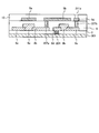
- the pixel 400 may have a top gate structure in which the gate electrodes 5a and 5b are formed on the organic EL element 24 side above the source electrodes 8a and 8d and the drain electrodes 8b and 8c.
- the pixel 400 includes a switching transistor 21 having a gate electrode 5a, a source electrode 8a, a drain electrode 8b, and a semiconductor film 9a, a gate electrode 5b, a source electrode 8d, and a drain electrode 8c. And a driving transistor 22 having a semiconductor film 9b, and an organic EL element 24 having an anode electrode 12, an organic film 13, and a cathode electrode 14.
- a gate insulating film 6 is formed between the source electrodes 8a and 8d, the drain electrodes 8b and 8c, the semiconductor films 9a and 9b, and the gate electrodes 5a and 5b.
- An interlayer insulating film 10 for absorbing the unevenness of each electrode is formed on the gate electrodes 5a and 5b.
- the pixel 400 has a top gate structure in which the gate electrodes 5a and 5b are formed on the organic EL element 24 side above the source electrodes 8a and 8d and the drain electrodes 8b and 8c.
- the substrate on which the switching transistor 21, the drive transistor 22, and the organic EL element 24 are provided is a metal substrate 301 that functions as a power supply line.
- the metal substrate 301 is connected to the source electrode 8 d of the drive transistor 22 through the in-contact wiring 204 formed in the interlayer insulating film 3.
- the drain electrode 8c of the drive transistor 22 is a connection film formed in the same layer as the in-contact wiring 207b and the gate electrodes 5a and 5b formed in the gate insulating film 6 and formed immediately above the in-contact wiring 207b.
- the electrode 5 is connected to the anode electrode 12 of the organic EL element 24 through the contact wiring 211 in the interlayer insulating film 10 formed immediately above the film 5d and the connection film 5d. Further, the gate electrode 5 b of the drive transistor 22 is connected to the drain electrode 8 b of the switching transistor 21 via the contact wiring 207 a formed in the gate insulating film 6.
- the capacitor 23 is formed by a partial region of the metal substrate 301, a partial region of the drain electrode 8b, and a partial region of the interlayer insulating film 3.
- the current is supplied to the organic EL element 24 using the metal substrate 301 existing in the entire display panel 603 without increasing the thickness of each electrode.
- the resistance of the metal substrate 301 functioning as a power supply line can be sufficiently reduced.
- the organic film 13 having a more uniform film thickness can be formed. It is possible to achieve the same effects as those of the pixel 300 that can achieve uniformization of the power consumption and reduce power consumption and prevent heat concentration.
- 14A to 14E are cross-sectional views illustrating a method for manufacturing the pixel 400 shown in FIG.
- the interlayer insulating film 3 is formed on the metal substrate 301 as in the case shown in FIG.
- a contact hole 204a is formed at a position corresponding to the source electrode 8d in the interlayer insulating film 3 by using a photolithography method. Then, as shown in FIG.
- the source electrodes 8a and 8d and the drain electrodes 8b After forming the in-contact wiring 204 by embedding a conductive material in the contact hole 204a, the source electrodes 8a and 8d and the drain electrodes 8b, In order to form 8c, a metal material, a transparent oxide conductive material, or the like is formed using a vacuum deposition method, a sputtering method, a coating method, or the like, and source electrodes 8a and 8d and a drain electrode are formed using a photolithography method, an etching method, or the like. 8b and 8c are patterned. The in-contact wiring 204, the source electrodes 8a and 8d, and the drain electrodes 8b and 8c can be formed in a lump.
- semiconductor films 9a and 9b are formed between the source electrodes 8a and 8d and the drain electrodes 8b and 8c.
- a gate insulating film 6 is formed in the same manner as described above.
- conductive materials are embedded in the contact holes 207c and 207d, thereby forming contact wirings 207a and 207b. To do.
- a metal material, a transparent oxide conductive material, or the like is applied to the gate insulating film using a vacuum deposition method, a sputtering method, or a coating method in order to form the gate electrodes 5a and 5b and the connection film 5d.
- 6 and the contact wirings 207a and 207b, the gate electrodes 5a and 5b and the connection film 5d are patterned using a photolithography method as shown in FIG. 14-4.
- the in-contact wirings 207a and 207b, the gate electrodes 5a and 5b, and the connection film 5d can be collectively formed.
- the contact hole 211a is formed in the interlayer insulating film 10. .
- the contact wiring 211 is formed by embedding a conductive material in the contact hole 211 a, the anode electrode 12 of the organic EL element 24 is formed, and then the organic film of the organic EL element 24 is formed. Is applied onto the anode electrode 12.
- the cathode electrode 14 is formed, the protective film 16 for protecting the organic EL element 24 is formed, and then the upper substrate 17 is provided on the protective film 16, whereby the pixel shown in FIG. 400 can be obtained.
- each electrode of each transistor is formed using a transparent electrode, and a substrate formed using a transparent conductor material instead of the metal substrate 301 may be used.
Landscapes
- Engineering & Computer Science (AREA)
- Microelectronics & Electronic Packaging (AREA)
- Physics & Mathematics (AREA)
- Optics & Photonics (AREA)
- Electroluminescent Light Sources (AREA)
- Devices For Indicating Variable Information By Combining Individual Elements (AREA)
Abstract
Description
[1] ゲート電極とソース電極とドレイン電極と前記ソース電極および前記ドレイン電極の間に形成された半導体膜とを含む半導体素子と、電極を含みかつ前記半導体素子に電気的に接続された発光素子と、前記半導体素子および前記発光素子が設けられる基板と、電源に接続されるとともに、前記基板の厚み方向から見て前記発光素子が設けられる領域を内包するように、前記半導体素子および前記発光素子と前記基板との間に形成された配線層と、前記半導体素子および前記発光素子と、前記配線層との間に設けられ、コンタクトホールが形成された層間絶縁膜と、前記コンタクトホール内に形成され、前記ソース電極、前記ドレイン電極および前記発光素子の前記電極のうちの少なくともいずれか一つと前記配線層とを電気的に接続するコンタクト内配線と、を備えたことを特徴とする表示装置。
[2] 前記配線層は、金属材料または酸化物導電材料から構成される、上記[1]に記載の表示装置。
[3] 前記半導体膜は、無機酸化物半導体材料から構成されている、上記[1]または[2]に記載の表示装置。
[4] 前記半導体膜は、有機半導体材料から構成される、上記[1]または[2]に記載の表示装置。
[5] 前記発光素子は、有機エレクトロルミネッセンス素子である、上記[1]~[4]のいずれか一つに記載の表示装置。
[6] 前記基板の厚み方向から見て、前記配線層は、前記発光素子が設けられる領域の全周から該領域の外方にはみ出すはみ出し領域を有する、上記[1]~[5]のいずれか一つに記載の表示装置。
[7] ゲート電極とソース電極とドレイン電極と前記ソース電極および前記ドレイン電極の間に形成された半導体膜とを含む半導体素子と、電極を有しかつ前記半導体素子に電気的に接続された発光素子と、前記半導体素子および前記発光素子が設けられる基板と、を備えた表示装置の製造方法であって、電源に接続されるとともに、前記基板の厚み方向から見て前記発光素子が設けられる領域を内包するように前記配線層を前記基板上に形成する配線層形成工程と、前記配線層を基準にして前記基板側と反対側に、層間絶縁膜を形成する層間絶縁膜形成工程と、前記層間絶縁膜を貫通し、一端が前記配線層に電気的に接続されたコンタクト内配線を形成するコンタクト内配線形成工程と、前記層間絶縁膜を基準にして前記基板側と反対側に、前記ソース電極と前記ドレイン電極とを形成する電極形成工程と、複数の前記発光素子を形成する発光素子形成工程と、を含み、前記ソース電極、前記ドレイン電極および前記発光素子の電極のうち少なくともいずれか一つは、前記コンタクト内配線の他端と電気的に接続されるように形成される、表示装置の製造方法。
が提供される。
まず、実施の形態1について説明する。図1は、本実施の形態1にかかる有機EL表示装置のブロック図の一例を示す図である。図1に示すように、実施の形態1にかかる有機EL表示装置は、ディスプレイパネル603、およびこれに接続される走査駆動部604、データ駆動部605、駆動電圧生成部607、並びにこれらを制御する信号制御部606を有する。ディスプレイパネル603は、走査駆動部604に接続され、各走査信号Vgを伝達する走査信号線G1、G2、G3、・・・、Gn、およびデータ駆動部605に接続され、各データ信号Vdを伝達するデータ信号線D1、D2、D3、・・・、Dmなどの複数の信号線に接続されている。各走査信号線G1~Gnは、略行方向に延伸しており、各データ信号線D1~Dmは、略列方向に延伸している。ディスプレイパネル603は、走査信号線G1~Gnおよび各データ信号線D1~Dmにそれぞれ接続されるように行列状に配列された複数の画素PXを備える。
配線層が平板状であり、かつはみ出し領域を有することの効果を確認するために行ったシミュレーション及びその結果について図15を参照して説明する。図15はシミュレーションに適用した基板および配線層のレイアウトの概略図である。
モデル(I)~モデル(III)の配線層をそれぞれ想定した等価回路において、電源端子2cに10Vの電圧を印加したときの動作についてシミュレーションを行った。5つのモニタ領域(第1モニタ領域2d1、第2モニタ領域2d2、第3モニタ領域2d3、第4モニタ領域2d4、及び第5モニタ領域2d5)のそれぞれについて電圧を算出した。図15では、第1~第5モニタ領域2d1~2d5をそれぞれ破線で囲まれた領域として示す。結果を表1に示す。

つぎに、本発明を実施するために参考となる他の実施の形態について説明する。図10は、本実施の形態にかかる有機EL表示装置の一画素を構成する各素子の断面を示した図である。なお、本実施の形態にかかる有機EL表示装置は、実施の形態1と同様に、図1に示す装置構成を有するとともに、各画素は、それぞれ図2に示す回路構成を有する。
2 配線層
2a,2b,2c 電極端子
2d1 第1モニタ領域
2d2 第2モニタ領域
2d3 第3モニタ領域
2d4 第4モニタ領域
2d5 第5モニタ領域
3 層間絶縁膜
4,7a,7b,11,111,204,207a,207b,211 コンタクト内配線
4a,7c,7d,11a,204a,207c,207d,211a コンタクトホール
5a,5b ゲート電極
5c,5d 接続膜
6 ゲート絶縁膜
8a,8d,108d ソース電極
8b,8c,108c ドレイン電極
9a,9b 半導体膜
10,110 層間絶縁膜
12 アノード電極
13 有機膜
14 カソード電極
16 保護膜
17 上部基板
21 スイッチングトランジスタ
22 駆動トランジスタ
23 キャパシタ
24 有機EL素子
100,200,300,400 画素
100a,300a 表示領域
100b,300b はみ出し領域
301 金属基板
318 絶縁膜
603 ディスプレイパネル
604 走査駆動部
605 データ駆動部
606 信号制御部
607 駆動電圧生成部
Claims (7)
- ゲート電極とソース電極とドレイン電極と前記ソース電極および前記ドレイン電極の間に形成された半導体膜とを含む半導体素子と、
電極を含みかつ前記半導体素子に電気的に接続された発光素子と、
前記半導体素子および前記発光素子が設けられる基板と、
電源に接続されるとともに、前記基板の厚み方向から見て前記発光素子が設けられる領域を内包するように、前記半導体素子および前記発光素子と前記基板との間に形成された配線層と、
前記半導体素子および前記発光素子と、前記配線層との間に設けられ、コンタクトホールが形成された層間絶縁膜と、
前記コンタクトホール内に形成され、前記ソース電極、前記ドレイン電極および前記発光素子の前記電極のうちの少なくともいずれか一つと前記配線層とを電気的に接続するコンタクト内配線と、
を備えたことを特徴とする表示装置。 - 前記配線層は、金属材料または酸化物導電材料から構成される、請求項1に記載の表示装置。
- 前記半導体膜は、無機酸化物半導体材料から構成されている、請求項1に記載の表示装置。
- 前記半導体膜は、有機半導体材料から構成される、請求項1に記載の表示装置。
- 前記発光素子は、有機エレクトロルミネッセンス素子である、請求項1に記載の表示装置。
- 前記基板の厚み方向から見て、前記配線層は、前記発光素子が設けられる領域の全周から該領域の外方にはみ出すはみ出し領域を有する、請求項1に記載の表示装置。
- ゲート電極とソース電極とドレイン電極と前記ソース電極および前記ドレイン電極の間に形成された半導体膜とを含む半導体素子と、
電極を有しかつ前記半導体素子に電気的に接続された発光素子と、
前記半導体素子および前記発光素子が設けられる基板と、を備えた表示装置の製造方法であって、
電源に接続されるとともに、前記基板の厚み方向から見て前記発光素子が設けられる領域を内包するように前記配線層を前記基板上に形成する配線層形成工程と、
前記配線層を基準にして前記基板側と反対側に、層間絶縁膜を形成する層間絶縁膜形成工程と、
前記層間絶縁膜を貫通し、一端が前記配線層に電気的に接続されたコンタクト内配線を形成するコンタクト内配線形成工程と、
前記層間絶縁膜を基準にして前記基板側と反対側に、前記ソース電極と前記ドレイン電極とを形成する電極形成工程と、
複数の前記発光素子を形成する発光素子形成工程と、
を含み、
前記ソース電極、前記ドレイン電極および前記発光素子の電極のうち少なくともいずれか一つは、前記コンタクト内配線の他端と電気的に接続されるように形成される、表示装置の製造方法。
Priority Applications (3)
| Application Number | Priority Date | Filing Date | Title |
|---|---|---|---|
| US13/056,082 US20110127537A1 (en) | 2008-07-30 | 2009-07-23 | Display device and method for manufacturing display device |
| CN2009801299200A CN102113040A (zh) | 2008-07-30 | 2009-07-23 | 显示装置及显示装置的制造方法 |
| EP09802882.2A EP2312562A4 (en) | 2008-07-30 | 2009-07-23 | DISPLAY DEVICE AND METHOD FOR PRODUCING A DISPLAY DEVICE |
Applications Claiming Priority (2)
| Application Number | Priority Date | Filing Date | Title |
|---|---|---|---|
| JP2008-195772 | 2008-07-30 | ||
| JP2008195772 | 2008-07-30 |
Publications (1)
| Publication Number | Publication Date |
|---|---|
| WO2010013639A1 true WO2010013639A1 (ja) | 2010-02-04 |
Family
ID=41610338
Family Applications (1)
| Application Number | Title | Priority Date | Filing Date |
|---|---|---|---|
| PCT/JP2009/063190 Ceased WO2010013639A1 (ja) | 2008-07-30 | 2009-07-23 | 表示装置および表示装置の製造方法 |
Country Status (7)
| Country | Link |
|---|---|
| US (1) | US20110127537A1 (ja) |
| EP (1) | EP2312562A4 (ja) |
| JP (1) | JP2010055070A (ja) |
| KR (1) | KR20110049783A (ja) |
| CN (1) | CN102113040A (ja) |
| TW (1) | TW201013922A (ja) |
| WO (1) | WO2010013639A1 (ja) |
Families Citing this family (12)
| Publication number | Priority date | Publication date | Assignee | Title |
|---|---|---|---|---|
| US8115883B2 (en) * | 2009-08-27 | 2012-02-14 | Semiconductor Energy Laboratory Co., Ltd. | Display device and method for manufacturing the same |
| TWI570809B (zh) | 2011-01-12 | 2017-02-11 | 半導體能源研究所股份有限公司 | 半導體裝置及其製造方法 |
| JP5806905B2 (ja) * | 2011-09-30 | 2015-11-10 | 株式会社半導体エネルギー研究所 | 半導体装置 |
| WO2013051236A1 (ja) * | 2011-10-05 | 2013-04-11 | パナソニック株式会社 | 表示装置 |
| FR3005754B1 (fr) * | 2013-05-17 | 2019-04-05 | Thales | Dispositif electrooptique a matrice de pixels de grande dimension |
| KR101844284B1 (ko) | 2013-10-07 | 2018-04-02 | 엘지디스플레이 주식회사 | 표시장치 및 그의 제조방법 |
| JP6098017B2 (ja) * | 2014-02-17 | 2017-03-22 | エバーディスプレイ オプトロニクス(シャンハイ) リミテッド | 薄膜トランジスタアレイ基板及びその製造方法 |
| JP6807712B2 (ja) * | 2016-11-16 | 2021-01-06 | 株式会社ジャパンディスプレイ | 表示装置 |
| CN109037273B (zh) * | 2017-06-08 | 2020-06-09 | 京东方科技集团股份有限公司 | 有机发光二极管阵列基板及其制备方法、显示装置 |
| CN113994485B (zh) * | 2019-05-10 | 2026-03-24 | 日亚化学工业株式会社 | 图像显示装置的制造方法以及图像显示装置 |
| KR102949676B1 (ko) * | 2020-10-05 | 2026-04-06 | 삼성전자주식회사 | 마이크로 발광 디스플레이 장치 및 그 제조 방법 |
| KR102802249B1 (ko) * | 2021-06-30 | 2025-05-07 | 엘지전자 주식회사 | 반도체 발광소자를 포함하는 디스플레이 장치 |
Citations (5)
| Publication number | Priority date | Publication date | Assignee | Title |
|---|---|---|---|---|
| JP2002032037A (ja) * | 2000-05-12 | 2002-01-31 | Semiconductor Energy Lab Co Ltd | 表示装置 |
| US20030111954A1 (en) * | 2001-12-14 | 2003-06-19 | Samsung Sdi Co., Ltd. | Flat panel display device with face plate and method for fabricating the same |
| JP2004046154A (ja) * | 2002-06-03 | 2004-02-12 | Lg Phillips Lcd Co Ltd | アクティブ・マトリクス有機電界発光素子及びその製造方法 |
| JP2004193129A (ja) * | 2002-12-11 | 2004-07-08 | Samsung Electronics Co Ltd | 有機発光表示板 |
| JP2005346055A (ja) | 2004-06-02 | 2005-12-15 | Samsung Electronics Co Ltd | 表示装置及びその駆動方法 |
Family Cites Families (9)
| Publication number | Priority date | Publication date | Assignee | Title |
|---|---|---|---|---|
| JP3082129B2 (ja) * | 1995-03-27 | 2000-08-28 | セイコーインスツルメンツ株式会社 | 液晶表示装置 |
| TW554637B (en) * | 2000-05-12 | 2003-09-21 | Semiconductor Energy Lab | Display device and light emitting device |
| US6835954B2 (en) * | 2001-12-29 | 2004-12-28 | Lg.Philips Lcd Co., Ltd. | Active matrix organic electroluminescent display device |
| KR100484591B1 (ko) * | 2001-12-29 | 2005-04-20 | 엘지.필립스 엘시디 주식회사 | 능동행렬 유기전기발광소자 및 그의 제조 방법 |
| JP4720069B2 (ja) * | 2002-04-18 | 2011-07-13 | セイコーエプソン株式会社 | 電気光学装置及び電子機器 |
| GB0220613D0 (en) * | 2002-09-05 | 2002-10-16 | Koninkl Philips Electronics Nv | Electroluminescent display devices |
| US7710019B2 (en) * | 2002-12-11 | 2010-05-04 | Samsung Electronics Co., Ltd. | Organic light-emitting diode display comprising auxiliary electrodes |
| JP4380242B2 (ja) * | 2003-07-16 | 2009-12-09 | セイコーエプソン株式会社 | 電気光学装置、電気光学装置の製造方法及び電子機器 |
| KR100768199B1 (ko) * | 2006-01-02 | 2007-10-17 | 삼성에스디아이 주식회사 | 유기 박막 트랜지스터 및 이를 구비한 유기 발광 표시 장치 |
-
2009
- 2009-07-07 JP JP2009160863A patent/JP2010055070A/ja active Pending
- 2009-07-23 CN CN2009801299200A patent/CN102113040A/zh active Pending
- 2009-07-23 KR KR1020117002216A patent/KR20110049783A/ko not_active Withdrawn
- 2009-07-23 US US13/056,082 patent/US20110127537A1/en not_active Abandoned
- 2009-07-23 WO PCT/JP2009/063190 patent/WO2010013639A1/ja not_active Ceased
- 2009-07-23 EP EP09802882.2A patent/EP2312562A4/en not_active Withdrawn
- 2009-07-29 TW TW098125488A patent/TW201013922A/zh unknown
Patent Citations (5)
| Publication number | Priority date | Publication date | Assignee | Title |
|---|---|---|---|---|
| JP2002032037A (ja) * | 2000-05-12 | 2002-01-31 | Semiconductor Energy Lab Co Ltd | 表示装置 |
| US20030111954A1 (en) * | 2001-12-14 | 2003-06-19 | Samsung Sdi Co., Ltd. | Flat panel display device with face plate and method for fabricating the same |
| JP2004046154A (ja) * | 2002-06-03 | 2004-02-12 | Lg Phillips Lcd Co Ltd | アクティブ・マトリクス有機電界発光素子及びその製造方法 |
| JP2004193129A (ja) * | 2002-12-11 | 2004-07-08 | Samsung Electronics Co Ltd | 有機発光表示板 |
| JP2005346055A (ja) | 2004-06-02 | 2005-12-15 | Samsung Electronics Co Ltd | 表示装置及びその駆動方法 |
Non-Patent Citations (1)
| Title |
|---|
| See also references of EP2312562A4 |
Also Published As
| Publication number | Publication date |
|---|---|
| TW201013922A (en) | 2010-04-01 |
| JP2010055070A (ja) | 2010-03-11 |
| CN102113040A (zh) | 2011-06-29 |
| US20110127537A1 (en) | 2011-06-02 |
| EP2312562A4 (en) | 2013-10-16 |
| KR20110049783A (ko) | 2011-05-12 |
| EP2312562A1 (en) | 2011-04-20 |
Similar Documents
| Publication | Publication Date | Title |
|---|---|---|
| WO2010013639A1 (ja) | 表示装置および表示装置の製造方法 | |
| CN102105924B (zh) | 显示装置以及显示装置的制造方法 | |
| US10671200B2 (en) | Display device and method of manufacturing the same | |
| US10504976B2 (en) | OLED display device and method of manufacturing the same | |
| US9287531B2 (en) | Organic light-emitting display device and method of manufacturing the same | |
| TW594636B (en) | Electro-optical device and electronic apparatus | |
| TWI478126B (zh) | Surface light display device | |
| US11107399B2 (en) | Organic light-emitting diode display device with pixel array | |
| JP7011149B2 (ja) | 表示装置及びその製造方法 | |
| CN102751311A (zh) | 有机电致发光显示装置 | |
| CN101405784A (zh) | El显示装置 | |
| JP6223070B2 (ja) | 有機el表示装置及び有機el表示装置の製造方法 | |
| TW201003600A (en) | Surface-emitting display device | |
| KR20180003363A (ko) | 유기발광 표시장치 | |
| CN110890386A (zh) | 薄膜晶体管基板、液晶显示装置及有机电致发光显示装置 | |
| TWI383344B (zh) | 顯示單元及其製造方法 | |
| US20080204377A1 (en) | Organic EL display device | |
| CN109728063B (zh) | 显示基板及显示装置 | |
| JP2010139640A (ja) | 表示装置 | |
| US11232949B2 (en) | Display device | |
| CN116386507A (zh) | 发光显示器 | |
| JP5212683B2 (ja) | トランジスタパネル及びその製造方法 | |
| JP5304761B2 (ja) | 発光装置及び電子機器 | |
| WO2025017861A1 (ja) | 表示装置 | |
| JP2010139641A (ja) | 表示装置 |
Legal Events
| Date | Code | Title | Description |
|---|---|---|---|
| WWE | Wipo information: entry into national phase |
Ref document number: 200980129920.0 Country of ref document: CN |
|
| 121 | Ep: the epo has been informed by wipo that ep was designated in this application |
Ref document number: 09802882 Country of ref document: EP Kind code of ref document: A1 |
|
| WWE | Wipo information: entry into national phase |
Ref document number: 13056082 Country of ref document: US |
|
| ENP | Entry into the national phase |
Ref document number: 20117002216 Country of ref document: KR Kind code of ref document: A |
|
| WWE | Wipo information: entry into national phase |
Ref document number: 2009802882 Country of ref document: EP |
|
| NENP | Non-entry into the national phase |
Ref country code: DE |