WO2010021202A1 - ニッケル粉末またはニッケルを主成分とする合金粉末およびその製造方法、導電性ペースト、並びに積層セラミックコンデンサ - Google Patents
ニッケル粉末またはニッケルを主成分とする合金粉末およびその製造方法、導電性ペースト、並びに積層セラミックコンデンサ Download PDFInfo
- Publication number
- WO2010021202A1 WO2010021202A1 PCT/JP2009/061701 JP2009061701W WO2010021202A1 WO 2010021202 A1 WO2010021202 A1 WO 2010021202A1 JP 2009061701 W JP2009061701 W JP 2009061701W WO 2010021202 A1 WO2010021202 A1 WO 2010021202A1
- Authority
- WO
- WIPO (PCT)
- Prior art keywords
- nickel
- powder
- alloy powder
- main component
- nickel powder
- Prior art date
- Legal status (The legal status is an assumption and is not a legal conclusion. Google has not performed a legal analysis and makes no representation as to the accuracy of the status listed.)
- Ceased
Links
Images


Classifications
-
- C—CHEMISTRY; METALLURGY
- C22—METALLURGY; FERROUS OR NON-FERROUS ALLOYS; TREATMENT OF ALLOYS OR NON-FERROUS METALS
- C22C—ALLOYS
- C22C19/00—Alloys based on nickel or cobalt
- C22C19/03—Alloys based on nickel or cobalt based on nickel
-
- B—PERFORMING OPERATIONS; TRANSPORTING
- B22—CASTING; POWDER METALLURGY
- B22F—WORKING METALLIC POWDER; MANUFACTURE OF ARTICLES FROM METALLIC POWDER; MAKING METALLIC POWDER; APPARATUS OR DEVICES SPECIALLY ADAPTED FOR METALLIC POWDER
- B22F1/00—Metallic powder; Treatment of metallic powder, e.g. to facilitate working or to improve properties
- B22F1/05—Metallic powder characterised by the size or surface area of the particles
- B22F1/054—Nanosized particles
- B22F1/056—Submicron particles having a size above 100 nm up to 300 nm
-
- B—PERFORMING OPERATIONS; TRANSPORTING
- B22—CASTING; POWDER METALLURGY
- B22F—WORKING METALLIC POWDER; MANUFACTURE OF ARTICLES FROM METALLIC POWDER; MAKING METALLIC POWDER; APPARATUS OR DEVICES SPECIALLY ADAPTED FOR METALLIC POWDER
- B22F9/00—Making metallic powder or suspensions thereof
- B22F9/16—Making metallic powder or suspensions thereof using chemical processes
- B22F9/18—Making metallic powder or suspensions thereof using chemical processes with reduction of metal compounds
- B22F9/24—Making metallic powder or suspensions thereof using chemical processes with reduction of metal compounds starting from liquid metal compounds, e.g. solutions
-
- B—PERFORMING OPERATIONS; TRANSPORTING
- B82—NANOTECHNOLOGY
- B82Y—SPECIFIC USES OR APPLICATIONS OF NANOSTRUCTURES; MEASUREMENT OR ANALYSIS OF NANOSTRUCTURES; MANUFACTURE OR TREATMENT OF NANOSTRUCTURES
- B82Y30/00—Nanotechnology for materials or surface science, e.g. nanocomposites
-
- H—ELECTRICITY
- H01—ELECTRIC ELEMENTS
- H01B—CABLES; CONDUCTORS; INSULATORS; SELECTION OF MATERIALS FOR THEIR CONDUCTIVE, INSULATING OR DIELECTRIC PROPERTIES
- H01B1/00—Conductors or conductive bodies characterised by the conductive materials; Selection of materials as conductors
- H01B1/02—Conductors or conductive bodies characterised by the conductive materials; Selection of materials as conductors mainly consisting of metals or alloys
-
- H—ELECTRICITY
- H01—ELECTRIC ELEMENTS
- H01B—CABLES; CONDUCTORS; INSULATORS; SELECTION OF MATERIALS FOR THEIR CONDUCTIVE, INSULATING OR DIELECTRIC PROPERTIES
- H01B1/00—Conductors or conductive bodies characterised by the conductive materials; Selection of materials as conductors
- H01B1/20—Conductive material dispersed in non-conductive organic material
- H01B1/22—Conductive material dispersed in non-conductive organic material the conductive material comprising metals or alloys
-
- H—ELECTRICITY
- H01—ELECTRIC ELEMENTS
- H01G—CAPACITORS; CAPACITORS, RECTIFIERS, DETECTORS, SWITCHING DEVICES, LIGHT-SENSITIVE OR TEMPERATURE-SENSITIVE DEVICES OF THE ELECTROLYTIC TYPE
- H01G4/00—Fixed capacitors; Processes of their manufacture
- H01G4/002—Details
- H01G4/005—Electrodes
- H01G4/008—Selection of materials
- H01G4/0085—Fried electrodes
-
- H—ELECTRICITY
- H01—ELECTRIC ELEMENTS
- H01G—CAPACITORS; CAPACITORS, RECTIFIERS, DETECTORS, SWITCHING DEVICES, LIGHT-SENSITIVE OR TEMPERATURE-SENSITIVE DEVICES OF THE ELECTROLYTIC TYPE
- H01G4/00—Fixed capacitors; Processes of their manufacture
- H01G4/30—Stacked capacitors
Definitions
- the present invention relates to a metal powder and a production method thereof, a conductive paste, and a multilayer ceramic capacitor, and more particularly, a metal powder suitable as a conductive fine powder for a conductive paste used for an internal electrode of a multilayer ceramic capacitor, a production method thereof,
- the present invention also relates to a conductive paste using the same, and a multilayer ceramic capacitor.
- metal powder has been used in various fields, and as a material for thick film conductors, it has been used for forming electric circuits such as electrodes of multilayer ceramic parts.
- the internal electrode of a multi-layer ceramic capacitor (MLCC) is formed using a conductive paste containing metal powder.
- This multilayer ceramic capacitor includes a ceramic body formed as a multilayer ceramic fired body by alternately stacking a plurality of dielectric layers and a plurality of conductive layers (internal electrode layers) by pressure bonding and firing and integrating them. A pair of external electrodes are formed at both ends of the ceramic body.
- a metal powder is mixed with an organic vehicle in which an organic binder such as a cellulose resin is dissolved in a solvent such as terpineol, and is kneaded and dispersed by a three-roll roll or the like, thereby conducting a conductive material for an internal electrode.
- a conductive paste this conductive paste is printed on a ceramic green sheet forming a dielectric layer, and the ceramic green sheet and the conductive paste layer (internal electrode layer) are alternately stacked by pressure bonding.
- a laminated ceramic fired body can be obtained by firing this laminated body in a reducing atmosphere.
- metals such as platinum, palladium, and silver-palladium alloys have been conventionally used as the metal powder contained in the conductive paste forming the internal electrode of the multilayer ceramic capacitor.
- these metals are expensive. For this reason, in recent years, inexpensive metals such as nickel have been used in order to reduce costs.
- a liquid phase reduction method in which metal ions are reduced with a reducing agent is used. More specifically, for example, a reducing agent aqueous solution containing a reducing agent is prepared, and a nickel aqueous solution containing nickel ions is mixed into the reducing agent aqueous solution to reduce nickel ions and deposit nickel powder.
- a reducing agent aqueous solution containing a reducing agent is prepared, and a nickel aqueous solution containing nickel ions is mixed into the reducing agent aqueous solution to reduce nickel ions and deposit nickel powder.
- the nickel powder produced by the above liquid phase reduction method has a low crystallinity because it is an aggregate of fine particles, and when an internal electrode of a multilayer ceramic capacitor is formed with a conductive paste containing nickel powder with low crystallinity.
- the shrinkage of the conductive paste containing nickel powder during firing increases, and as the sintering progresses, the conductive paste breaks into islands, causing electrode breaks (breaks in internal electrodes), and multilayer ceramic
- the capacitance of the capacitor is reduced.
- the present invention has been made in view of the above problems, and a multilayer ceramic capacitor having an internal electrode whose surface is smoothed and which can reliably prevent electrode breakage, a conductive paste used therein, nickel powder or
- An object is to provide an alloy powder containing nickel as a main component and a method for producing the same.
- the average particle diameter D 50 is 30 to 300 nm
- the half width of the diffraction peak of the (111) plane by X-ray diffraction method is 0.5 ° or less
- the ratio of the specific surface area A measured by the BET method to the theoretical value B of the specific surface area corresponding to the average particle diameter D 50 (A / B) is 3 or less
- nickel powder or nickel as a main component Alloy powder is 3 or less.
- the surface of the nickel powder that is the metal powder or the alloy powder containing nickel as a main component is smoothed and the crystallinity is improved, so the nickel powder or the alloy powder containing nickel as a main component is contained. Even when the internal electrode is formed by the conductive paste, the electrode surface can be easily smoothed and the occurrence of electrode breakage can be avoided.
- the second invention of the present application is to reduce the nickel ions by the reducing agent in a reaction solution containing nickel ions, a reducing agent, and a dispersing agent, and to make the whole nickel powder or the whole alloy powder mainly composed of nickel.
- it is a method for producing nickel powder or nickel-based alloy powder, characterized by comprising at least a step of performing heat treatment at 300 ° C. to 700 ° C.
- a third invention of the present application is a method for producing a nickel powder or an alloy powder containing nickel as a main component according to the second invention of the present application, wherein the heat treatment is performed in a reducing atmosphere containing 2% or more of H 2 gas.
- a fourth invention of the present application is a conductive paste characterized in that the nickel powder of the first invention of the present application or an alloy powder containing nickel as a main component and an organic vehicle as main components.
- a fifth invention of the present application is a multilayer ceramic capacitor comprising a capacitor body formed by alternately laminating internal electrode layers and dielectric layers, wherein the internal electrode layer is formed by the conductive paste of the fourth invention of the present application It is characterized by being.
- the internal electrode of the multilayer ceramic capacitor is formed by the conductive paste containing the nickel powder or the nickel-based alloy powder of the present invention, the electrode surface is easily smoothed and the electrode is interrupted. Can be avoided.
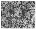
- FIG. 2 is an electron micrograph showing nickel powder in Example 1.
- FIG. 2 is an electron micrograph showing nickel powder in Comparative Example 1.
- 4 is an electron micrograph showing nickel powder in Comparative Example 2.
- 6 is an electron micrograph showing nickel powder in Comparative Example 3.
- the metal powder according to the present invention is used as a conductive powder for a conductive paste used for an internal electrode of a multilayer ceramic capacitor.
- a method for producing a metal powder according to the present invention it can be produced by a liquid phase reduction method in which metal ions in an aqueous solution are reduced and a metal compound is subjected to a wet reduction treatment.
- a water-soluble metal compound is added to and dissolved in water or a mixture of water and a lower alcohol to prepare an aqueous solution containing metal ions, a dispersant is added to the aqueous solution, and then the reducing agent is dissolved. It is possible to prepare a reaction solution to which the aqueous solution is added, stir the reaction solution, and then perform a heat treatment for improving crystallinity.
- the metal powder when producing a nickel powder or a nickel-based alloy powder as the metal powder, contains a metal ion (nickel ion) in which a nickel salt (for example, nickel sulfate) as a metal compound is dissolved in pure water, An aqueous solution to which a dispersant is added and a titanium ion aqueous solution containing trivalent titanium ions that act as a reducing agent are mixed at a predetermined ratio to prepare a reaction solution, and then hydroxylated as a pH adjuster in the reaction solution. A sodium aqueous solution is added to adjust the pH, and stirring is performed to reduce nickel ions and precipitate nickel powder or alloy powder containing nickel as a main component. And in order to improve the crystallinity of nickel powder or the alloy powder which has nickel as a main component, it manufactures by performing heat processing in a reducing atmosphere.
- nickel ion nickel ion
- a nickel salt for example, nickel sulfate
- a metal compound for example, nickel
- the metal powder according to the present invention is not particularly limited, but nickel powder and alloy powder mainly composed of nickel are preferably used. This is because nickel powder or alloy powder containing nickel as a main component is excellent in conductivity, low in cost, and excellent in oxidation resistance as compared with other metals such as copper. This is because it is less likely to occur and is suitable as a conductive material.
- the alloy powder of nickel for example, an alloy powder of nickel and at least one element selected from the group consisting of manganese, chromium, cobalt, aluminum, iron, copper, zinc, gold, platinum, silver, and palladium Can be used. Further, the content of nickel in the alloy powder containing nickel as a main component is 50% by mass or more, preferably 80% by mass or more. This is because if the nickel content is reduced, oxidation is likely to occur during firing, and therefore, electrode breakage, a decrease in capacitance, and the like are likely to occur.
- the metal powder according to the present invention for use as a conductive powder for a conductive paste used in internal electrodes of multilayer ceramic capacitors, average particle diameter D 50 of the alloy powder based on nickel powder or nickel Those having a thickness of 30 to 300 nm can be used.
- the nickel salt to be used is not particularly limited.
- a nickel salt containing at least one selected from the group consisting of nickel sulfate, nickel chloride, nickel nitrate, nickel acetate, nickel sulfamate, and nickel hydroxide can be used.
- nickel chloride is preferably used from the viewpoint that it contains the same chlorine ions as titanium trichloride, which is a reducing agent.
- the concentration of nickel salt in the reaction solution is preferably 5 g / l or more and 100 g / l or less. This is because when the nickel salt concentration is less than 5 g / l, it is difficult to reduce and precipitate a sufficient amount of nickel powder, resulting in a decrease in productivity, and the nickel salt concentration from 100 g / l. If it is large, the collision probability between the nickel particles increases, so that the particles are likely to aggregate, and there is a case where it is difficult to control the particle size.
- titanium trichloride sodium borohydride, hydrazine and the like can be used.
- titanium trichloride having strong reducibility to metal ions and reduce metal ions using an aqueous titanium ion solution containing trivalent titanium ions.
- the pH adjuster is not particularly limited as long as it is conventionally used in the nickel powder reduction precipitation process. More specifically, as the pH adjuster, for example, sodium hydroxide, sodium carbonate, ammonia and the like can be used.
- the entire nickel powder or an alloy containing nickel as a main component is used to prevent coarsening due to heat treatment and increase crystallinity. It is set as the structure which heat-processes in the reducing atmosphere the nickel powder containing 0.1 to 5 mass% of carbon with respect to the whole powder, or the alloy powder which has nickel as a main component.
- the half width of the diffraction peak of the (111) plane by the X-ray diffraction method is used as the crystallinity index of the nickel powder of the present invention or the alloy powder containing nickel as a main component. Then, by using the production method of the present invention, a nickel powder or a nickel-based alloy powder whose half-value width of the diffraction peak of the (111) plane by X-ray diffraction is 0.5 ° or less is obtained. Therefore, the crystallinity of the nickel powder or the alloy powder containing nickel as a main component is improved. As a result, even when the internal electrode is formed by the conductive paste containing nickel powder or an alloy powder containing nickel as a main component, it is possible to avoid the occurrence of electrode breakage.
- the specific surface area is used as an indicator of the smoothness of the nickel powder or the alloy powder containing nickel as a main component of the present invention. More specifically, the specific surface area A [m 2 / g] of the nickel powder or nickel-based alloy powder measured by the BET method and the average particle diameter of the nickel powder or nickel-based alloy powder The theoretical value B [m 2 / g] of the specific surface area corresponding to D 50 is used. And by using the manufacturing method of this invention, the ratio (A / B) of the specific surface area A and the theoretical value B of a specific surface area is 3 or less nickel powder or the alloy powder which has nickel as a main component. Therefore, the smoothness of the nickel powder or the alloy powder containing nickel as a main component is improved. As a result, even when the internal electrode is formed with a conductive paste containing nickel powder or an alloy powder containing nickel as a main component, the surface of the electrode can be easily smoothed.
- the “BET method” mentioned here is one of powder surface measurement methods by vapor phase adsorption, and the total surface area (ie, specific surface area) of a 1 g sample is determined by using an adsorption isotherm. This is a calculation method and is a well-known method.
- B [m 2 / g] of the specific surface area corresponding to the average particle diameter D 50 of the nickel powder or the alloy powder containing nickel as a main component can be obtained by the following (Equation 1).
- B [m 2 / g] 6 / (D50 [um] ⁇ ⁇ [g / cm 3 ]) (Formula 1)
- ⁇ is a density.
- the average particle diameter D 50 of the nickel powder or the alloy powder containing nickel as a main component measured using a SEM (scanning electron microscope) is 100 nm and the density is 8.9 g / cm 3 , the above (formula From 1), the theoretical value B [m 2 / g] of the specific surface area is 6.7 [m 2 / g].
- the specific surface area A [m 2 / g] of the nickel powder or nickel-based alloy powder measured by the BET method is 16 [m 2 / g]
- the specific surface area A and the theoretical value B of the specific surface area B (A / B) is 2.4, and in this case, it can be said that the nickel powder or the alloy powder containing nickel as a main component is excellent in surface smoothness.
- a carbon-containing dispersant is used to obtain a carbon-containing nickel powder or an alloy powder containing nickel as a main component by the above-described liquid phase reduction method.
- the dispersant used the dispersibility of the nickel powder or nickel-based alloy powder in the reaction solution is improved, and the reduction-precipitated nickel powder or nickel-based alloy powder has carbon on the surface. If it can adsorb
- polyvinyl pyrrolidone which is a polymer dispersant, polycarboxylic acid type anionic dispersant, polyvinyl alcohol, cationic dispersant and the like can be used.
- the carbon content with respect to the whole nickel powder or the whole alloy powder containing nickel as a main component is set to 0.1 mass% or more and 5 mass% or less when the carbon content is less than 0.1 mass%.
- the carbon may not be sufficiently adsorbed on the surface of the nickel powder reduced or precipitated or the alloy powder containing nickel as a main component, and the above-described coarsening prevention effect and crystallinity improvement effect may not be sufficiently obtained.
- the carbon content is more than 5% by mass, it may remain without being decomposed during the heat treatment.
- the heat treatment of the nickel powder containing carbon or the alloy powder mainly containing nickel produced by the above-described liquid phase reduction method is performed in order to suppress the oxidation of the nickel powder or the alloy powder mainly containing nickel.
- the atmosphere in the reducing atmosphere and the heat treatment is preferably a reducing atmosphere containing 2% or more of H 2 gas (for example, an atmosphere of a mixed gas of N 2 gas and H 2 gas).
- the temperature during the heat treatment is preferably 300 ° C. to 700 ° C., and more preferably 400 ° C. to 600 ° C.
- the holding time of the above temperature at the time of heat treatment is 0.5 hours to 3 hours.
- the conductive paste of the present invention contains the above-described nickel powder of the present invention or an alloy powder containing nickel as a main component and an organic vehicle as main components.
- the organic vehicle used in the present invention is a mixture of a resin and a solvent.
- the resin examples include cellulose resins such as methyl cellulose, ethyl cellulose, nitrocellulose, cellulose acetate, and cellulose propionate, methyl (meth) acrylate, ( Acrylic esters such as ethyl (meth) acrylate and propyl (meth) acrylate, alkyd resins, polyvinyl alcohol, and the like can be used, and ethyl cellulose is particularly preferably used from the viewpoints of safety and stability.
- the solvent constituting the organic vehicle terpineol, tetralin, butyl carbitol, carbitol acetate, etc. can be used alone or in combination.
- a conductive paste for example, an organic vehicle in which an organic binder of a cellulose resin is dissolved in terpineol is produced, and then the nickel powder of the present invention or an alloy powder containing nickel as a main component and the organic vehicle are produced.
- the conductive paste for the internal electrode of the multilayer ceramic capacitor of the present invention can be obtained.
- a dielectric material, an additive for adjusting sintering, and the like can be added to the conductive paste.
- a multilayer ceramic capacitor is obtained by alternately laminating a plurality of dielectric layers made of ceramic green sheets and a plurality of internal electrode layers made of conductive paste by pressure bonding, and then firing the laminate. By integrating them. After producing a multilayer ceramic fired body to be a ceramic body, it is manufactured by forming a pair of external electrodes at both ends of the ceramic body.
- a ceramic green sheet that is an unfired ceramic sheet is prepared.
- this ceramic green sheet for example, a dielectric layer paste obtained by adding an organic binder such as polyvinyl butyral and a solvent such as terpineol to a predetermined ceramic raw material powder such as barium titanate, a PET film or the like. Examples thereof include a sheet formed on a support film and dried to remove the solvent.
- the thickness of the dielectric layer made of the ceramic green sheet is not particularly limited, but is preferably 0.2 ⁇ m to 4 ⁇ m from the viewpoint of demand for downsizing of the multilayer ceramic capacitor.
- a plurality of sheets are prepared by printing and applying the above-described conductive paste on one side of the ceramic green sheet by a known method such as a screen printing method to form an internal electrode layer made of the conductive paste.
- the thickness of the internal electrode layer made of a conductive paste is preferably 0.2 to 4 ⁇ m or less from the viewpoint of the demand for thinning of the internal electrode layer.
- the ceramic green sheet is peeled off from the support film, and heating and heating are performed so that the dielectric layer made of the ceramic green sheet and the internal electrode layer made of the conductive paste formed on one surface thereof are alternately arranged.
- Lamination is performed by pressure treatment to obtain a laminate.
- the green chip is subjected to a binder removal treatment and fired in a reducing atmosphere to produce a laminated ceramic fired body.
- the atmosphere in the debinding process is preferably air or an N 2 gas atmosphere, and the temperature during the debinding process is preferably 200 ° C. to 400 ° C. Further, it is preferable that the temperature holding time at the time of performing the binder removal treatment is 0.5 to 24 hours.
- the firing is performed in a reducing atmosphere in order to suppress oxidation of the metal used for the internal electrode layer, and the atmosphere at the time of firing is an atmosphere of N 2 gas or a mixed gas of N 2 gas and H 2 gas.
- the temperature at which the laminate is fired is preferably 1250 ° C. to 1350 ° C.
- the holding time of the above temperature when firing is preferably 0.5 to 8 hours.
- the organic binder in the green sheet is removed, and the ceramic raw material powder is fired to form a ceramic dielectric layer. Further, the organic vehicle in the internal electrode layer is removed, and the nickel powder or the alloy powder containing nickel as a main component is sintered or melted and integrated to form an internal electrode, and the dielectric layer, the internal electrode layer, A multilayer ceramic fired body in which a plurality of sheets are alternately laminated is formed.
- the atmosphere in the annealing treatment is preferably an N 2 gas atmosphere, and the temperature during the annealing treatment is preferably set to 800 ° C. to 950 ° C. Further, it is preferable that the temperature holding time at the time of annealing is 2 hours to 10 hours.
- a multilayer ceramic capacitor is manufactured by providing a pair of external electrodes to the manufactured multilayer ceramic fired body.
- a material of an external electrode copper, nickel, or these alloys can be used conveniently, for example.
- the alloy powder based on nickel powder or nickel an average particle diameter D 50 of 30 ⁇ 300 nm, the half-width of the diffraction peak of the (111) plane by X-ray diffraction method 0. 5 ° or less and the ratio of the theoretical value B of a corresponding specific surface has been a specific surface area a mean particle diameter D 50 measured by the BET method (a / B) is configured to be 3 or less.
- the surface of the nickel powder which is a metal powder, or an alloy powder containing nickel as a main component is smoothed and the crystallinity is improved, so that the conductive paste containing nickel powder or an alloy powder containing nickel as a main component is provided.
- the electrode surface can be easily smoothed and the occurrence of electrode breakage can be avoided.
- nickel ions are reduced by a reducing agent in a reaction solution containing nickel ions, a reducing agent, and a dispersing agent.
- the deposited nickel powder or alloy powder containing nickel as a main component is subjected to heat treatment at 300 ° C. to 700 ° C.
- the heat treatment is performed in a reducing atmosphere containing 2% or more of H 2 gas. Therefore, during the heat treatment, oxidation of the nickel powder or the alloy powder containing nickel as a main component can be suppressed.
- Example 1 (Production of nickel powder) Nickel sulfate hexahydrate as a metal compound is dissolved in pure water so as to have a concentration of 20 g / l, and an aqueous solution containing nickel ions is prepared.
- polyvinylpyrrolidone molymer (molecular weight 30000) is used as a dispersant. It added so that it might become a density
- titanium chloride as a reducing agent was dissolved in pure water to a concentration of 80 g / l to prepare a titanium ion aqueous solution containing trivalent titanium ions. Then, these aqueous solutions are mixed to prepare a reaction solution.
- sodium hydroxide is dissolved in pure water as a pH adjuster so as to have a concentration of 10 g / l. Was added to adjust the pH of the reaction solution to 9.0.
- this reaction solution was reacted at a reaction temperature of 30 ° C. for 120 minutes with stirring at a speed of 500 rpm, whereby nickel powder was reduced and precipitated. Subsequently, the reaction solution was subjected to suction filtration, and impurities were removed while repeating washing with pure water to obtain a nickel dispersion solution having no precipitation using water as a dispersion medium. And the nickel powder was produced by drying this nickel dispersion liquid. Note that in precipitated nickel powder was 120nm was measured an average particle size D 50 of when observed at a magnification of 30,000 using a scanning electron microscope. Moreover, when the amount of carbon contained in the nickel powder was measured using a high frequency combustion infrared absorption method, it was 1.5% by mass with respect to the whole nickel powder.
- the deposited nickel powder was heat-treated at a temperature of 500 ° C. in a reducing atmosphere (H 2 gas was 3%, N 2 gas was 97%).
- the holding time during the heat treatment was set to 1 hour.
- the average particle diameter D 50 of when observed at a magnification of 30,000 using a scanning electron microscope to measure a 150 nm coarsening of the nickel powder is not observed It was.
- the theoretical value B [m 2 / g] of the specific surface area corresponding to the average particle diameter D 50 of the nickel powder after the heat treatment was determined from the above (formula 1), it was 4.5 [m 2 / g]. there were.
- the specific surface area A [m 2 / g] of the nickel powder after the heat treatment measured by the BET method is 10 [m 2 / g], and the specific surface area A and the average particle diameter D 50 measured by the BET method.
- the ratio (A / B) of the specific surface area corresponding to to the theoretical value B was 2.2. Accordingly, it was confirmed that the nickel powder after the heat treatment was excellent in surface smoothness. Furthermore, when the crystallinity of the nickel powder after heat treatment was evaluated by the X-ray diffraction method, the half-value width of the diffraction peak of the (111) plane was 0.25 °, and it was confirmed that the crystallinity was high. An electron micrograph of the nickel powder obtained in this example is shown in FIG.
- an organic vehicle is prepared by dissolving 10 parts by mass of ethyl cellulose, which is an organic binder, in 90 parts by mass of terpineol, and 100 parts by mass of the nickel powder after the above heat treatment and 40 parts by mass of the organic vehicle are mixed and kneaded by three rolls. -By dispersing, a conductive paste for the internal electrode of the multilayer ceramic capacitor was produced.
- a dielectric layer paste (barium titanate, which is a ceramic raw material powder, to which ethyl cellulose as an organic binder and terpineol as a solvent are added) is applied in a sheet form on a PET film, which is a support film, Next, drying was performed to remove the solvent, thereby producing a ceramic green sheet having a thickness of 2 ⁇ m. Next, the produced conductive paste was printed on one side of the ceramic green sheet by a screen printing method and applied to form an internal electrode layer made of the conductive paste having a thickness of 2 ⁇ m.
- the ceramic green sheet is peeled from the PET film and a protective ceramic green sheet is laminated on the surface of the internal electrode layer of the peeled ceramic green sheet and pressed to form a dielectric layer composed of the ceramic green sheet and the conductive layer.
- a laminate was produced in which internal electrode layers made of paste were alternately laminated.
- the manufactured multilayer body is cut into a predetermined size (0.3 mm ⁇ 0.6 mm) to form a green chip, and then the green chip is subjected to binder removal processing, firing, and annealing treatment to form a multilayer ceramic as a capacitor body.
- a fired body was produced.
- the binder removal treatment was performed in an air atmosphere at a temperature of 300 ° C. and a holding time of 1 hour.
- Firing was performed in an N 2 gas atmosphere at a temperature of 1300 ° C. and a holding time of 2 hours.
- the annealing treatment was performed in a N 2 gas atmosphere at a temperature of 900 ° C. and a holding time of 1 hour.
- Example 2 (Production of nickel powder)
- Nickel acetate tetrahydrate as a metal compound is dissolved in pure water so as to have a concentration of 25 g / l, and an aqueous solution containing nickel ions is prepared.
- polyvinyl alcohol molecular weight 10,000
- titanium chloride as a reducing agent was dissolved in pure water to a concentration of 80 g / l to prepare a titanium ion aqueous solution containing trivalent titanium ions. Then, these aqueous solutions are mixed to prepare a reaction solution.
- this reaction solution was reacted at a reaction temperature of 30 ° C. for 120 minutes with stirring at a speed of 500 rpm, whereby nickel powder was reduced and precipitated.
- cross flow ultrafiltration was performed on the reaction solution, and impurities were removed while repeating washing with pure water, to obtain a nickel dispersion solution with no precipitation using water as a dispersion medium.
- the nickel powder was produced by drying this nickel dispersion liquid. Note that in precipitated nickel powder was 30nm was measured an average particle size D 50 of when observed at a magnification of 30,000 using a scanning electron microscope. Further, when the amount of carbon contained in the nickel powder was measured using a high frequency combustion infrared absorption method, it was 4% by mass with respect to the whole nickel powder.
- the deposited nickel powder was heat-treated at a temperature of 350 ° C. in a reducing atmosphere (3% H 2 gas and 97% N 2 gas).
- the holding time during the heat treatment was set to 1 hour.
- the average particle diameter D 50 of when observed at a magnification of 30,000 using a scanning electron microscope to measure a 40 nm coarsening of the nickel powder is not observed It was.
- the theoretical value B [m 2 / g] of the specific surface area corresponding to the average particle diameter D 50 of the nickel powder after the heat treatment was determined from the above (formula 1), it was 16.8 [m 2 / g]. there were.
- the specific surface area A [m 2 / g] of the nickel powder after the heat treatment measured by the BET method is 33.6 [m 2 / g]
- the specific surface area A and the average particle diameter measured by the BET method are 33.6 [m 2 / g].
- the ratio of the theoretical value B of specific surface area corresponding to D 50 (a / B) was 2.0. Accordingly, it was confirmed that the nickel powder after the heat treatment was excellent in surface smoothness.
- the crystallinity of the nickel powder after the heat treatment was evaluated by the X-ray diffraction method, the half-value width of the diffraction peak of the (111) plane was 0.45 °, and it was confirmed that the crystallinity was high.
- Example 1 a conductive paste, internal electrodes, a multilayer body, and a multilayer ceramic fired body were obtained. Then, the above results of performing the smoothness evaluation of the electrode surface and the electrode breakage evaluation under the same conditions as in Example 1 are shown in Table 1.
- Example 1 A nickel powder was produced in the same manner as in Example 1 except that the heat treatment was not performed. Note that in the nickel powder produced was measured an average particle size D 50 of when observed at a magnification of 30,000 using a scanning electron microscope was 120 nm. From the above (Equation 1), the theoretical value B [m 2 / g] of the specific surface area corresponding to the average particle diameter D 50 of the prepared nickel powder was determined to be 5.6 [m 2 / g]. It was. Further, the specific surface area A [m 2 / g] of the nickel powder measured by the BET method is 15.7 [m 2 / g], and the specific surface area A and the average particle diameter D 50 measured by the BET method are as follows.
- the ratio (A / B) of the corresponding specific surface area to the theoretical value B was 2.8. Accordingly, it was confirmed that the nickel powder after the heat treatment was excellent in surface smoothness. Furthermore, when the crystallinity of the nickel powder after the heat treatment was evaluated by the X-ray diffraction method, the half-value width of the diffraction peak of the (111) plane was 1.5 °, and it was confirmed that the crystallinity was low. An electron micrograph of the nickel powder obtained in this example is shown in FIG. Moreover, it carried out similarly to the above-mentioned Example 1, and obtained the electrically conductive paste, the internal electrode, the laminated body, and the laminated ceramic fired body. Then, the above results of performing the smoothness evaluation of the electrode surface and the electrode breakage evaluation under the same conditions as in Example 1 are shown in Table 1.
- Nickel powder was produced in the same manner as in Example 1 except that the temperature during the heat treatment was set to 100 ° C. Note that in the nickel powder before the heat treatment, when the average particle diameter D 50 of when observed at a magnification of 30,000 using a scanning electron microscope was measured to be 120 nm. Further, in the nickel powder after the heat treatment, when the average particle diameter D 50 of when observed at a magnification of 30,000 using a scanning electron microscope to measure a 120 nm, coarsening of the nickel powder is not observed It was. From the above (Equation 1), the theoretical value B [m 2 / g] of the specific surface area corresponding to the average particle diameter D 50 of the prepared nickel powder was determined to be 5.6 [m 2 / g].
- the specific surface area A [m 2 / g] of the nickel powder measured by the BET method is 14 [m 2 / g], and corresponds to the specific surface area A and the average particle diameter D 50 measured by the BET method.
- the ratio (A / B) of the specific surface area to the theoretical value B was 2.5. Accordingly, it was confirmed that the nickel powder after the heat treatment was excellent in surface smoothness. Furthermore, when the crystallinity of the nickel powder after the heat treatment was evaluated by the X-ray diffraction method, the half-value width of the diffraction peak of the (111) plane was 0.8 °, and it was confirmed that the crystallinity was low.
- An electron micrograph of the nickel powder obtained in this example is shown in FIG.
- Example 1 it carried out similarly to the above-mentioned Example 1, and obtained the electrically conductive paste, the internal electrode, the laminated body, and the laminated ceramic fired body. Then, the above results of performing the smoothness evaluation of the electrode surface and the electrode breakage evaluation under the same conditions as in Example 1 are shown in Table 1.
- Example 3 A nickel powder was produced in the same manner as in Example 1 except that the temperature during the heat treatment was set to 800 ° C. Note that in the nickel powder before the heat treatment, when the average particle diameter D 50 of when observed at a magnification of 30,000 using a scanning electron microscope was measured to be 200 nm. Further, in the nickel powder after the heat treatment, when the average particle diameter D 50 of when observed using a scanning electron microscope at a magnification of 30000 times was measured, a 800 nm, coarsening of the nickel powder was observed.
- the theoretical value B [m 2 / g] of the specific surface area corresponding to the average particle diameter D 50 of the produced nickel powder was determined from the above (Formula 1), it was 0.8 [m 2 / g]. It was. Moreover, the specific surface area A [m 2 / g] of the nickel powder measured by the BET method is 3.6 [m 2 / g], and the specific surface area A and the average particle diameter D 50 measured by the BET method are as follows. The ratio (A / B) of the corresponding specific surface area to the theoretical value B was 4.5. Therefore, it was confirmed that the nickel powder after the heat treatment has low surface smoothness.
- the nickel powder of Example 1 is not an agglomerated powder and is excellent in surface smoothness. Further, as shown in Table 1, it can be seen that the internal electrode formed of the conductive paste containing the nickel powder of Example 1 has excellent surface smoothness and no electrode breakage. From the above, it can be said that the conductive paste containing the nickel powder of Example 1 is excellent in forming the internal electrode of the multilayer ceramic capacitor.
- the nickel particles of Comparative Example 1 are not agglomerated powder and are excellent in surface smoothness.
- Table 1 it can be seen that the internal electrode formed of the conductive paste containing the nickel powder of Comparative Example 1 has an electrode discontinuity. This is presumably because, in Comparative Example 1, the deposited nickel particles were not heat-treated, and the crystallinity of the nickel powder was low.
- the nickel particles of Comparative Example 2 are not agglomerated powder and are excellent in surface smoothness.
- Table 1 it can be seen that the internal electrode formed of the conductive paste containing the nickel powder of Comparative Example 1 has an electrode discontinuity. This is because, in Comparative Example 2, the deposited nickel particles were heat treated. However, since the heat treatment temperature was as low as 100 ° C., single crystallization did not proceed sufficiently and the crystallinity of the nickel powder was not sufficiently improved.
- the nickel particles of Comparative Example 3 are coarse and have poor surface smoothness.
- Table 1 it can be seen that the internal electrode formed of the conductive paste containing the nickel powder of Comparative Example 3 has poor surface smoothness.
- the deposited nickel particles were heat-treated, but since the heat treatment temperature was as high as 800 ° C., single crystallization proceeded, but the particles joined together and aggregated. This is considered to be because it became powder.
- nickel powder or an alloy powder containing nickel as a main component and a method for producing the same, a conductive paste, and a multilayer ceramic capacitor in particular, a conductive paste for a conductive paste used for an internal electrode of the multilayer ceramic capacitor.
Landscapes
- Engineering & Computer Science (AREA)
- Chemical & Material Sciences (AREA)
- Nanotechnology (AREA)
- Power Engineering (AREA)
- Materials Engineering (AREA)
- Inorganic Chemistry (AREA)
- Microelectronics & Electronic Packaging (AREA)
- Physics & Mathematics (AREA)
- Manufacturing & Machinery (AREA)
- Chemical Kinetics & Catalysis (AREA)
- Dispersion Chemistry (AREA)
- Spectroscopy & Molecular Physics (AREA)
- General Chemical & Material Sciences (AREA)
- Condensed Matter Physics & Semiconductors (AREA)
- Crystallography & Structural Chemistry (AREA)
- General Physics & Mathematics (AREA)
- Composite Materials (AREA)
- Mechanical Engineering (AREA)
- Metallurgy (AREA)
- Organic Chemistry (AREA)
- Ceramic Capacitors (AREA)
- Powder Metallurgy (AREA)
- Fixed Capacitors And Capacitor Manufacturing Machines (AREA)
- Manufacture Of Metal Powder And Suspensions Thereof (AREA)
- Conductive Materials (AREA)
- Non-Insulated Conductors (AREA)
Abstract
Description
本願第4の発明は、本願第1の発明のニッケル粉末またはニッケルを主成分とする合金粉末と、有機ビヒクルを主成分とすることを特徴とする導電性ペーストである。
B〔m2/g〕=6/(D50〔um〕×ρ〔g/cm3〕)…(式1)
ここで、(式1)中、ρは、密度である。
(1)本実施形態においては、ニッケル粉末またはニッケルを主成分とする合金粉末が、平均粒径D50が30~300nm、X線回折法による(111)面の回折ピークの半値幅が0.5°以下であり、かつBET法により測定された比表面積Aと平均粒径D50に対応する比表面積の理論値Bとの比(A/B)が3以下である構成としている。従って、金属粉末であるニッケル粉末またはニッケルを主成分とする合金粉末の表面が平滑化されるとともに、結晶性が向上するため、ニッケル粉末またはニッケルを主成分とする合金粉末を含有する導電性ペーストにより、内部電極を形成する場合であっても、電極表面の平滑化が容易になるとともに、電極途切れの発生を回避することが可能になる。
(ニッケル粉末の作製)
金属化合物としての硫酸ニッケル六水和物を、20g/lの濃度となるように純水に溶解させ、ニッケルイオンを含む水溶液を作製し、この水溶液に分散剤としてポリビニルピロリドン(分子量30000)を、4g/lの濃度となるように添加した。次いで、還元剤としての塩化チタンを、80g/lの濃度となるように純水に溶解させ、3価のチタンイオンを含むチタンイオン水溶液を作製した。そして、これらの水溶液を混合して、反応液を作製し、この反応液に、pH調整剤として、水酸化ナトリウムを、10g/lの濃度となるように純水に溶解させた水酸化ナトリウム水溶液を加えて、反応液のpHが9.0となるように調整した。
次いで、有機バインダーであるエチルセルロース10質量部をターピネオール90質量部に溶解させた有機ビヒクルを作製し、上述の熱処理後のニッケル粉末100質量部と有機ビヒクル40質量部を混合し、三本ロールによって混練・分散することにより、積層セラミックコンデンサの内部電極用の導電性ペーストを作製した。
まず、誘電体層用ペースト(セラミックの原料粉末であるチタン酸バリウムに、有機バインダーであるエチルセルロースと溶剤であるターピネオールとを加えたもの)を支持フィルムであるPETフィルム上にシート状に塗布し、次いで、乾燥させて溶剤を除去することにより、厚みが2μmであるセラミックグリーンシートを作製した。次いで、このセラミックグリーンシートの片面に、スクリーン印刷法により、上述の作製した導電性ペーストを印刷して塗布し、導電性ペーストからなる厚みが2μmである内部電極層を形成した。次いで、PETフィルムからセラミックグリーンシートを剥離するとともに、剥離したセラミックグリーンシートの内部電極層の表面上に保護用のセラミックグリーンシートを積層、圧着して、セラミックグリーンシートからなる誘電体層と導電性ペーストからなる内部電極層とが交互に積層された積層体を作製した。
製作した積層体を所定サイズ(0.3mm×0.6mm)に切断してグリーンチップを形成後、当該グリーンチップに対して脱バインダー処理、焼成、およびアニール処理を行い、コンデンサ本体である積層セラミック焼成体を作製した。なお、脱バインダー処理は、大気雰囲気において、300℃の温度で、保持時間を1時間として行った。また、焼成は、N2ガス雰囲気において、1300℃の温度で、保持時間を2時間として行った。また、アニール処理は、N2ガス雰囲気において、900℃の温度で、保持時間を1時間として行った。
次いで、製作した積層セラミック焼成体を切断し、その断面を、走査型電子顕微鏡を使用して観察(倍率:2000倍、視野:50μm×60μm)して、電極の平滑性、および電極途切れの有無を目視により判断した。その結果を表1に示す。
(ニッケル粉末の作製)
金属化合物としての酢酸ニッケル四水和物を、25g/lの濃度となるように純水に溶解させ、ニッケルイオンを含む水溶液を作製し、この水溶液に分散剤としてポリビニルアルコール(分子量10000)を、4g/lの濃度となるように添加した。次いで、還元剤としての塩化チタンを、80g/lの濃度となるように純水に溶解させ、3価のチタンイオンを含むチタンイオン水溶液を作製した。そして、これらの水溶液を混合して、反応液を作製し、この反応液に、pH調整剤として、炭酸ナトリウムを、20g/lの濃度となるように純水に溶解させた水酸化ナトリウム水溶液を加えて、反応液のpHが8.5となるように調整した。
熱処理を行わなかったこと以外は、上述の実施例1と同様にして、ニッケル粉末を作製した。なお、作製したニッケル粉末において、走査型電子顕微鏡を使用して倍率30000倍にて観察した時の平均粒径D50を測定したところ、120nmであった。また、上記(式1)より、作製したニッケル粉末の平均粒径D50に対応する比表面積の理論値B〔m2/g〕を求めたところ、5.6〔m2/g〕であった。また、BET法により測定されたニッケル粉末の比表面積A〔m2/g〕は、15.7〔m2/g〕であり、BET法により測定された比表面積Aと平均粒径D50に対応する比表面積の理論値Bとの比(A/B)は、2.8であった。従って、熱処理後のニッケル粉末は、表面平滑性に優れていることが確認された。さらに、X線回折法により、熱処理後のニッケル粉末の結晶性を評価したところ、(111)面の回折ピークの半値幅が1.5°となり、結晶性が低いことが確認された。なお、本実施例で得られたニッケル粉末の電子顕微鏡写真を図2に示す。また、上述の実施例1と同様にして、導電性ペースト、内部電極、積層体、および積層セラミック焼成体を得た。その後、上述の実施例1と同一条件により、電極表面の平滑性評価、および電極途切れ評価を行った、以上の結果を表1に示す。
熱処理を行う際の温度を100℃に設定したこと以外は、上述の実施例1と同様にして、ニッケル粉末を作製した。なお、熱処理前のニッケル粉末において、走査型電子顕微鏡を使用して倍率30000倍にて観察した時の平均粒径D50を測定したところ、120nmであった。また、熱処理後のニッケル粉末において、走査型電子顕微鏡を使用して倍率30000倍にて観察した時の平均粒径D50を測定したところ、120nmであり、ニッケル粉末の粗大化は、見られなかった。また、上記(式1)より、作製したニッケル粉末の平均粒径D50に対応する比表面積の理論値B〔m2/g〕を求めたところ、5.6〔m2/g〕であった。また、BET法により測定されたニッケル粉末の比表面積A〔m2/g〕は、14〔m2/g〕であり、BET法により測定された比表面積Aと平均粒径D50に対応する比表面積の理論値Bとの比(A/B)は、2.5であった。従って、熱処理後のニッケル粉末は、表面平滑性に優れていることが確認された。さらに、X線回折法により、熱処理後のニッケル粉末の結晶性を評価したところ、(111)面の回折ピークの半値幅が0.8°となり、結晶性が低いことが確認された。なお、本実施例で得られたニッケル粉末の電子顕微鏡写真を図3に示す。また、上述の実施例1と同様にして、導電性ペースト、内部電極、積層体、および積層セラミック焼成体を得た。その後、上述の実施例1と同一条件により、電極表面の平滑性評価、および電極途切れ評価を行った、以上の結果を表1に示す。
熱処理を行う際の温度を800℃に設定したこと以外は、上述の実施例1と同様にして、ニッケル粉末を作製した。なお、熱処理前のニッケル粉末において、走査型電子顕微鏡を使用して倍率30000倍にて観察した時の平均粒径D50を測定したところ、200nmであった。また、熱処理後のニッケル粉末において、走査型電子顕微鏡を使用して倍率30000倍にて観察した時の平均粒径D50を測定したところ、800nmであり、ニッケル粉末の粗大化が見られた。また、上記(式1)より、作製したニッケル粉末の平均粒径D50に対応する比表面積の理論値B〔m2/g〕を求めたところ、0.8〔m2/g〕であった。また、BET法により測定されたニッケル粉末の比表面積A〔m2/g〕は、3.6〔m2/g〕であり、BET法により測定された比表面積Aと平均粒径D50に対応する比表面積の理論値Bとの比(A/B)は、4.5であった。従って、熱処理後のニッケル粉末は、表面平滑性が低いことが確認された。さらに、X線回折法により、熱処理後のニッケル粉末の結晶性を評価したところ、(111)面の回折ピークの半値幅が0.1°となり、結晶性が高いことが確認された。なお、本実施例で得られたニッケル粉末の電子顕微鏡写真を図4に示す。また、上述の実施例1と同様にして、導電性ペースト、内部電極、積層体、および積層セラミック焼成体を得た。その後、上述の実施例1と同一条件により、電極表面の平滑性評価、および電極途切れ評価を行った、以上の結果を表1に示す。

が、熱処理温度が100℃と低温であったため、単結晶化が十分に進行せず、ニッケル粉末の結晶性が十分に向上しなかったためであると考えられる。
Claims (5)
- 平均粒径D50が30~300nm、X線回折法による(111)面の回折ピークの半値幅が0.5°以下であり、かつBET法により測定された比表面積Aと前記平均粒径D50に対応する比表面積の理論値Bとの比(A/B)が3以下であることを特徴とするニッケル粉末またはニッケルを主成分とする合金粉末。
- ニッケルイオンと、還元剤と、分散剤とを含む反応液中で、前記還元剤により前記ニッケルイオンを還元させて、ニッケル粉末全体またはニッケルを主成分とする合金粉末全体に対して0.1質量%以上5質量%以下の炭素を含有するニッケル粉末またはニッケルを主成分とする合金粉末を析出させる工程と、
前記析出させたニッケル粉末またはニッケルを主成分とする合金粉末に対して、300℃~700℃で熱処理を行う工程と
を少なくとも含むことを特徴とするニッケル粉末またはニッケルを主成分とする合金粉末の製造方法。 - H2ガスを2%以上含む還元雰囲気中で、前記熱処理を行うことを特徴とする請求項2に記載のニッケル粉末またはニッケルを主成分とする合金粉末の製造方法。
- 請求項1に記載のニッケル粉末またはニッケルを主成分とする合金粉末と、有機ビヒクルを主成分とすることを特徴とする導電性ペースト。
- 内部電極層および誘電体層を交互に積層して形成されたコンデンサ本体を備える積層セラミックコンデンサであって、
前記内部電極層が、請求項4に記載の導電性ペーストにより形成されていることを特徴とする積層セラミックコンデンサ。
Priority Applications (3)
| Application Number | Priority Date | Filing Date | Title |
|---|---|---|---|
| US13/059,323 US20110141654A1 (en) | 2008-08-18 | 2009-06-26 | Nickel powder or alloy powder comprising nickel as main component, method for producing the same, conductive paste and laminated ceramic capacitor |
| EP09808138A EP2314400A1 (en) | 2008-08-18 | 2009-06-26 | Nickel powder or alloy powder comprising nickel as main component, method for producing the same, conductive paste and laminated ceramic capacitor |
| CN2009801324560A CN102123805A (zh) | 2008-08-18 | 2009-06-26 | 镍粉或包含镍作为主要成分的合金粉末、其制备方法、导电性糊状物、以及层压陶瓷电容器 |
Applications Claiming Priority (2)
| Application Number | Priority Date | Filing Date | Title |
|---|---|---|---|
| JP2008-209997 | 2008-08-18 | ||
| JP2008209997A JP2010043345A (ja) | 2008-08-18 | 2008-08-18 | ニッケル粉末またはニッケルを主成分とする合金粉末およびその製造方法、導電性ペースト、並びに積層セラミックコンデンサ |
Publications (1)
| Publication Number | Publication Date |
|---|---|
| WO2010021202A1 true WO2010021202A1 (ja) | 2010-02-25 |
Family
ID=41707081
Family Applications (1)
| Application Number | Title | Priority Date | Filing Date |
|---|---|---|---|
| PCT/JP2009/061701 Ceased WO2010021202A1 (ja) | 2008-08-18 | 2009-06-26 | ニッケル粉末またはニッケルを主成分とする合金粉末およびその製造方法、導電性ペースト、並びに積層セラミックコンデンサ |
Country Status (7)
| Country | Link |
|---|---|
| US (1) | US20110141654A1 (ja) |
| EP (1) | EP2314400A1 (ja) |
| JP (1) | JP2010043345A (ja) |
| KR (1) | KR20110059700A (ja) |
| CN (1) | CN102123805A (ja) |
| TW (1) | TW201016350A (ja) |
| WO (1) | WO2010021202A1 (ja) |
Cited By (2)
| Publication number | Priority date | Publication date | Assignee | Title |
|---|---|---|---|---|
| KR20160082253A (ko) | 2014-03-20 | 2016-07-08 | 세키스이가가쿠 고교가부시키가이샤 | 도전 페이스트 |
| JP2021141131A (ja) * | 2020-03-03 | 2021-09-16 | 太陽誘電株式会社 | セラミック電子部品の製造方法、および金属導電ペースト |
Families Citing this family (14)
| Publication number | Priority date | Publication date | Assignee | Title |
|---|---|---|---|---|
| JP2013042104A (ja) * | 2011-07-19 | 2013-02-28 | Sumitomo Electric Ind Ltd | 積層セラミックコンデンサ用の導電ペーストおよびその製造方法 |
| JP5794426B2 (ja) * | 2011-11-30 | 2015-10-14 | 戸田工業株式会社 | ニッケル微粒子粉末の製造法 |
| JP2013115425A (ja) * | 2011-11-30 | 2013-06-10 | Samsung Electro-Mechanics Co Ltd | 積層セラミック電子部品及びその製造方法 |
| KR20140023543A (ko) * | 2012-08-16 | 2014-02-27 | 삼성전기주식회사 | 내부 전극용 니켈 분말, 그 제조방법 및 이를 포함하는 적층 세라믹 전자부품 |
| CN104837580B (zh) * | 2012-11-20 | 2016-10-26 | 杰富意矿物股份有限公司 | 镍粉末、导电膏以及层叠陶瓷电子部件 |
| KR102029478B1 (ko) * | 2013-07-29 | 2019-10-07 | 삼성전기주식회사 | 내부 전극 페이스트 조성물, 및 이를 내부전극층으로 이용한 적층형 세라믹 캐패시터 |
| JP6135935B2 (ja) * | 2014-03-28 | 2017-05-31 | 住友金属鉱山株式会社 | 湿式ニッケル粉末の製造方法 |
| JP6846969B2 (ja) * | 2016-03-31 | 2021-03-24 | Dowaエレクトロニクス株式会社 | 銀被覆ニッケル粉末およびその製造方法 |
| US10395841B2 (en) * | 2016-12-02 | 2019-08-27 | Capacitor Sciences Incorporated | Multilayered electrode and film energy storage device |
| CN110461503B (zh) * | 2017-03-10 | 2022-01-14 | 东邦钛株式会社 | 镍粉和镍糊料 |
| CN110799285B (zh) * | 2017-07-05 | 2022-04-29 | 东邦钛株式会社 | 金属粉末及其制造方法 |
| KR20250012192A (ko) * | 2018-01-30 | 2025-01-23 | 테크나 플라즈마 시스템 인코포레이티드 | 다층 세라믹 커패시터의 전극 재료로 사용하기 위한 금속 분말과 제조 방법 및 그 사용 방법 |
| JP7193534B2 (ja) * | 2018-06-28 | 2022-12-20 | 東邦チタニウム株式会社 | ニッケル粉体とその製造方法 |
| KR20230008405A (ko) * | 2021-07-07 | 2023-01-16 | 삼성전기주식회사 | 커패시터 부품 및 커패시터 부품의 제조 방법 |
Citations (5)
| Publication number | Priority date | Publication date | Assignee | Title |
|---|---|---|---|---|
| JPH11302709A (ja) | 1998-04-24 | 1999-11-02 | Murata Mfg Co Ltd | ニッケルまたはニッケル合金微粉末の製造方法 |
| JP2003105402A (ja) * | 2001-09-28 | 2003-04-09 | Mitsui Mining & Smelting Co Ltd | 導電ペースト用の銅粉及びその銅粉を用いた導電ペースト並びにその導電ペーストを用いた導体を含んだチップ部品 |
| JP2004176120A (ja) * | 2002-11-27 | 2004-06-24 | Sumitomo Metal Mining Co Ltd | 導電粉末、その製造方法、及びそれを用いた導電ペースト |
| JP2005154904A (ja) * | 2003-11-25 | 2005-06-16 | Samsung Electronics Co Ltd | 炭素含有ニッケル粒子粉末およびその製造方法 |
| JP2008095146A (ja) * | 2006-10-12 | 2008-04-24 | Akita Prefecture | 球状ニッケル微小粒子およびその製造方法ならびに、異方性導電フィルム用導電粒子 |
Family Cites Families (1)
| Publication number | Priority date | Publication date | Assignee | Title |
|---|---|---|---|---|
| TWI399254B (zh) * | 2004-12-10 | 2013-06-21 | Mitsui Mining & Smelting Co | Nickel powder and its manufacturing method and conductive paste |
-
2008
- 2008-08-18 JP JP2008209997A patent/JP2010043345A/ja active Pending
-
2009
- 2009-06-26 EP EP09808138A patent/EP2314400A1/en not_active Withdrawn
- 2009-06-26 KR KR1020117002812A patent/KR20110059700A/ko not_active Withdrawn
- 2009-06-26 CN CN2009801324560A patent/CN102123805A/zh active Pending
- 2009-06-26 WO PCT/JP2009/061701 patent/WO2010021202A1/ja not_active Ceased
- 2009-06-26 US US13/059,323 patent/US20110141654A1/en not_active Abandoned
- 2009-08-17 TW TW098127526A patent/TW201016350A/zh unknown
Patent Citations (5)
| Publication number | Priority date | Publication date | Assignee | Title |
|---|---|---|---|---|
| JPH11302709A (ja) | 1998-04-24 | 1999-11-02 | Murata Mfg Co Ltd | ニッケルまたはニッケル合金微粉末の製造方法 |
| JP2003105402A (ja) * | 2001-09-28 | 2003-04-09 | Mitsui Mining & Smelting Co Ltd | 導電ペースト用の銅粉及びその銅粉を用いた導電ペースト並びにその導電ペーストを用いた導体を含んだチップ部品 |
| JP2004176120A (ja) * | 2002-11-27 | 2004-06-24 | Sumitomo Metal Mining Co Ltd | 導電粉末、その製造方法、及びそれを用いた導電ペースト |
| JP2005154904A (ja) * | 2003-11-25 | 2005-06-16 | Samsung Electronics Co Ltd | 炭素含有ニッケル粒子粉末およびその製造方法 |
| JP2008095146A (ja) * | 2006-10-12 | 2008-04-24 | Akita Prefecture | 球状ニッケル微小粒子およびその製造方法ならびに、異方性導電フィルム用導電粒子 |
Cited By (4)
| Publication number | Priority date | Publication date | Assignee | Title |
|---|---|---|---|---|
| KR20160082253A (ko) | 2014-03-20 | 2016-07-08 | 세키스이가가쿠 고교가부시키가이샤 | 도전 페이스트 |
| US9796866B2 (en) | 2014-03-20 | 2017-10-24 | Sekisui Chemical Co., Ltd. | Electroconductive paste |
| JP2021141131A (ja) * | 2020-03-03 | 2021-09-16 | 太陽誘電株式会社 | セラミック電子部品の製造方法、および金属導電ペースト |
| JP7523922B2 (ja) | 2020-03-03 | 2024-07-29 | 太陽誘電株式会社 | セラミック電子部品の製造方法、および金属導電ペースト |
Also Published As
| Publication number | Publication date |
|---|---|
| JP2010043345A (ja) | 2010-02-25 |
| KR20110059700A (ko) | 2011-06-03 |
| US20110141654A1 (en) | 2011-06-16 |
| TW201016350A (en) | 2010-05-01 |
| EP2314400A1 (en) | 2011-04-27 |
| CN102123805A (zh) | 2011-07-13 |
Similar Documents
| Publication | Publication Date | Title |
|---|---|---|
| WO2010021202A1 (ja) | ニッケル粉末またはニッケルを主成分とする合金粉末およびその製造方法、導電性ペースト、並びに積層セラミックコンデンサ | |
| JP5407495B2 (ja) | 金属粉末および金属粉末製造方法、導電性ペースト、並びに積層セラミックコンデンサ | |
| JP2009079239A (ja) | ニッケル粉末、またはニッケルを主成分とする合金粉末およびその製造方法、導電性ペースト、並びに積層セラミックコンデンサ | |
| JP4081987B2 (ja) | 金属粉末の製造方法,金属粉末,これを用いた導電性ペーストならびにこれを用いた積層セラミック電子部品 | |
| JP5843821B2 (ja) | 金属粉ペースト、及びその製造方法 | |
| JP2010053409A (ja) | 金属粉末の製造方法および金属粉末、導電性ペースト、積層セラミックコンデンサ | |
| JP5574154B2 (ja) | ニッケル粉末およびその製造方法 | |
| WO2001033588A1 (fr) | Condensateur multicouche | |
| JP6799936B2 (ja) | ニッケル粒子、導電性ペースト、内部電極及び積層セラミックコンデンサ | |
| US20160203911A1 (en) | Surface-treated metal powder, and method for producing same | |
| KR100859646B1 (ko) | 도전성 입자의 제조 방법, 도전성 페이스트 및 전자 부품의제조 방법 | |
| JP4100244B2 (ja) | ニッケル粉末とその製造方法 | |
| JP2015036444A (ja) | 表面処理された金属粉の製造方法 | |
| JP2015036443A (ja) | 表面処理された金属粉の製造方法 | |
| JP5206246B2 (ja) | ニッケル粉末およびその製造方法 | |
| JP5526856B2 (ja) | ニッケル粉末およびその製造方法 | |
| CN118742982A (zh) | 层叠陶瓷电子部件 | |
| JP2014231643A (ja) | 金属粉末の製造方法、金属粉末及び積層セラミックコンデンサ用導電性ペースト | |
| JP2013067865A (ja) | 金属粉末、導電性ペースト及び積層セラミックコンデンサ | |
| JP2020084275A (ja) | ニッケル粉末 | |
| JP2004247632A (ja) | 導電性ペースト、及び積層セラミックコンデンサ | |
| JP5348918B2 (ja) | ニッケル粉末、卑金属粉末の製法、導体ペースト、ならびに電子部品 | |
| JP4453214B2 (ja) | 銅粉末の製造方法、銅粉末、導電性ペーストおよびセラミック電子部品 | |
| JP2017119906A (ja) | ニッケル微粒子含有組成物及びその製造方法、内部電極並びに積層セラミックスコンデンサ | |
| JP3922001B2 (ja) | 銅粉末の製造方法、銅粉末、導電性ペースト、及び積層セラミック電子部品 |
Legal Events
| Date | Code | Title | Description |
|---|---|---|---|
| WWE | Wipo information: entry into national phase |
Ref document number: 200980132456.0 Country of ref document: CN |
|
| 121 | Ep: the epo has been informed by wipo that ep was designated in this application |
Ref document number: 09808138 Country of ref document: EP Kind code of ref document: A1 |
|
| ENP | Entry into the national phase |
Ref document number: 20117002812 Country of ref document: KR Kind code of ref document: A |
|
| WWE | Wipo information: entry into national phase |
Ref document number: 13059323 Country of ref document: US |
|
| WWE | Wipo information: entry into national phase |
Ref document number: 2009808138 Country of ref document: EP |
|
| NENP | Non-entry into the national phase |
Ref country code: DE |