WO2010038735A1 - 基板検出装置および方法 - Google Patents
基板検出装置および方法 Download PDFInfo
- Publication number
- WO2010038735A1 WO2010038735A1 PCT/JP2009/066938 JP2009066938W WO2010038735A1 WO 2010038735 A1 WO2010038735 A1 WO 2010038735A1 JP 2009066938 W JP2009066938 W JP 2009066938W WO 2010038735 A1 WO2010038735 A1 WO 2010038735A1
- Authority
- WO
- WIPO (PCT)
- Prior art keywords
- substrates
- substrate detection
- light source
- illumination
- reflector
- Prior art date
- Legal status (The legal status is an assumption and is not a legal conclusion. Google has not performed a legal analysis and makes no representation as to the accuracy of the status listed.)
- Ceased
Links
Images





Classifications
-
- H—ELECTRICITY
- H10—SEMICONDUCTOR DEVICES; ELECTRIC SOLID-STATE DEVICES NOT OTHERWISE PROVIDED FOR
- H10P—GENERIC PROCESSES OR APPARATUS FOR THE MANUFACTURE OR TREATMENT OF DEVICES COVERED BY CLASS H10
- H10P72/00—Handling or holding of wafers, substrates or devices during manufacture or treatment thereof
- H10P72/06—Apparatus for monitoring, sorting, marking, testing or measuring
- H10P72/0606—Position monitoring, e.g. misposition detection or presence detection
- H10P72/0608—Position monitoring, e.g. misposition detection or presence detection of substrates stored in a container, a magazine, a carrier, a boat or the like
-
- H—ELECTRICITY
- H10—SEMICONDUCTOR DEVICES; ELECTRIC SOLID-STATE DEVICES NOT OTHERWISE PROVIDED FOR
- H10P—GENERIC PROCESSES OR APPARATUS FOR THE MANUFACTURE OR TREATMENT OF DEVICES COVERED BY CLASS H10
- H10P72/00—Handling or holding of wafers, substrates or devices during manufacture or treatment thereof
-
- H—ELECTRICITY
- H10—SEMICONDUCTOR DEVICES; ELECTRIC SOLID-STATE DEVICES NOT OTHERWISE PROVIDED FOR
- H10P—GENERIC PROCESSES OR APPARATUS FOR THE MANUFACTURE OR TREATMENT OF DEVICES COVERED BY CLASS H10
- H10P72/00—Handling or holding of wafers, substrates or devices during manufacture or treatment thereof
- H10P72/50—Handling or holding of wafers, substrates or devices during manufacture or treatment thereof for positioning, orientation or alignment
-
- Y—GENERAL TAGGING OF NEW TECHNOLOGICAL DEVELOPMENTS; GENERAL TAGGING OF CROSS-SECTIONAL TECHNOLOGIES SPANNING OVER SEVERAL SECTIONS OF THE IPC; TECHNICAL SUBJECTS COVERED BY FORMER USPC CROSS-REFERENCE ART COLLECTIONS [XRACs] AND DIGESTS
- Y10—TECHNICAL SUBJECTS COVERED BY FORMER USPC
- Y10S—TECHNICAL SUBJECTS COVERED BY FORMER USPC CROSS-REFERENCE ART COLLECTIONS [XRACs] AND DIGESTS
- Y10S414/00—Material or article handling
- Y10S414/135—Associated with semiconductor wafer handling
- Y10S414/137—Associated with semiconductor wafer handling including means for charging or discharging wafer cassette
- Y10S414/138—Wafers positioned vertically within cassette
Definitions
- the present invention relates to an apparatus and a method for detecting a storage state of a plurality of substrates stored in a cassette.
- the present invention is suitable for detecting the storage state of a plurality of semiconductor wafers stored in a wafer cassette (FOUP).
- FOUP wafer cassette
- a method of detecting the storage state of a plurality of wafers stored in a wafer cassette As a method of detecting the storage state of a plurality of wafers stored in a wafer cassette (FOUP), a method is used in which a wafer end is mechanically scanned by a transmission optical switch and mapping is performed by detection of light shielding (light shielding type). Sensor scan) is known.
- a mapping sensor method using such an image there is a method of acquiring and analyzing a plurality of luminance profile lines between two points perpendicular to the wafer surface.
- mapping method based on the light-shielding sensor scan is simple, but it is essential to attach the sensor to the mechanism part, and it takes a relatively long time for the mechanical scan. It is necessary to additionally install a dedicated sensor.
- jumping detection refers to detecting a state in which the wafer stored in the wafer cassette is protruding forward from the specified storage position.
- the presence / absence of the wafer and the cross wafer are determined from the position and interval of the peak (capturing the reflection at the wafer edge), so that the local There is a problem of being vulnerable to disturbances.
- the present invention has been made in view of the above-described problems of the prior art, and provides a substrate detection apparatus and method that can quickly and reliably detect the storage state of a plurality of substrates in a cassette. With the goal.
- the present invention provides an apparatus for detecting a storage state of a plurality of substrates housed in a cassette, a collimator reflector disposed beside the plurality of substrates, and the collimator reflection.
- An illuminating unit that emits light in a plane toward a plate, the illuminating unit disposed so that ends of the plurality of substrates are positioned in an optical path thereof, and a plane radiated from the illuminating unit.
- the illumination means includes a surface light source.
- the illumination unit includes a point light source that emits light toward the collimator reflector, and a retroreflector that reflects the collimated light reflected by the collimator reflector toward the collimator reflector. And including.
- the point light source and the image pickup means are disposed substantially coaxially with each other.
- the surface light source or the point light source includes a light emitting diode.
- the collimating reflector is a parabolic mirror.
- the collimating reflector is composed of a curved mirror formed by combining a plurality of flat mirrors as a whole into a substantially curved shape.
- the present invention provides a method for detecting a storage state of a plurality of substrates stored in a cassette from an illumination unit toward a collimator reflector disposed beside the plurality of substrates.
- the illumination means includes a surface light source.
- light emitted from a point light source toward the collimator reflector, and reflected and collimated by the collimator reflector is provided in the optical path so that end portions of the plurality of substrates are in the optical path. Reflected by the retroreflector toward the collimator reflector so as to be positioned.
- the point light source and the image pickup means are disposed substantially coaxially with each other.
- the surface light source or the point light source includes a light emitting diode.
- the collimating reflector is a parabolic mirror.
- the collimating reflector is composed of a curved mirror formed by combining a plurality of flat mirrors as a whole into a substantially curved shape.
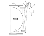
- the substrate detection apparatus 1 is for detecting the storage state of a plurality of semiconductor wafers (substrates) 11 stored in a FOUP (wafer cassette) 10. .
- the semiconductor wafer 11 has a circular flat plate shape, and is carried in and out of the FOUP 10 by a hand attached to the tip of the arm of the wafer transfer robot.
- a high-luminance point light source 2 composed of a light emitting diode (LED) is disposed substantially coaxially with an imaging means 3 composed of a CCD camera (monocular camera).
- LED light emitting diode
- the light from the point light source 2 is radiated toward the collimating reflector 4 formed of a radiation mirror, reflected by the collimator reflector 4 and collimated.
- the collimating reflector 4 can also be constituted by a curved mirror formed by combining a plurality of small flat mirrors in a substantially curved shape as a whole, instead of the parabolic mirror.
- a retroreflecting plate 5 is disposed so as to face the collimating reflecting plate 4, and the retroreflecting plate 5 is configured by a ⁇ CCR plate (CCR: “Corner” Cube “Reflector”).
- the imaging means 3 is connected to the image processing means 6 by a transmission cable, and an image acquired by the imaging means 3 is transmitted to the image processing means 6 via the transmission cable.
- the light from the point light source 2 is radiated, reflected by the collimating reflector 4 and collimated.
- the light reflected by the collimator reflector 4 is reflected toward the collimator reflector 4 by the retroreflector 5 disposed opposite to the collimator reflector 4 (irradiation step).
- the illumination transmission image including the ends of the plurality of wafers 11 is formed on the collimator reflector 4 by the light reflected by the retroreflector 4. That is, the ends of the plurality of wafers 11 are positioned in the optical path of the reflected light that is reflected by the retroreflecting plate 5 and directed toward the collimating reflecting plate 4.
- the illumination transmission image including the ends of the plurality of wafers 11 projected on the collimating reflector 4 is picked up by the image pickup means 3 composed of a CCD camera (image pickup step).
- the mirror normal of the collimating reflector 4 and the camera optical axis of the image pickup means (CCD camera) 3 are parallel to each other on the plan view. Forms a parallel image.
- FIG. 2 is an image diagram of the illumination transmission image 20 on the collimator reflection plate 4 acquired by the imaging means 3.
- the portions shielded by the respective end portions of the plurality of wafers 11 appear as a plurality of local light shielding portions (low luminance portions). Therefore, by analyzing the illumination transmission image 20 by the image processing means 6, it is possible to detect the storage state of the plurality of wafers 11 in the cassette 10 (detection step).
- the pop-out amount can be determined.
- double wafer refers to the case where two wafers are stored in the same slot.
- Cross wafer refers to a case where wafers are stored in different levels in the left and right slots.
- the “pop-out wafer” refers to a case where the wafer is jumping forward from a specified storage position.
- the corresponding light-shielding portion when there is no wafer in a certain slot, the corresponding light-shielding portion is missing. Further, when a pop-out wafer is present, the light shielding portion corresponding thereto is longer in the Y-axis direction than the other light shielding portions. When there is a cross wafer, the light shielding portion corresponding to the cross wafer is thicker in the X-axis direction than the other light shielding portions, and extends over two slot positions. When a double wafer is present, a portion corresponding to the double wafer is twice as thick in the X-axis direction as the other light shielding portions.
- This embodiment employs an image processing method using a camera, but in principle, is close to a method of scanning a transmission type light shielding sensor, and therefore depends on the reflectance of the wafer 11 as an object. Therefore, the storage state of the wafer 11 can be reliably detected.
- the illumination transmission image 20 can be obtained with a certain width (length in the Y-axis direction) at the edge of the wafer 11, the projection of the wafer 11 can be reliably detected in addition to the function of the mapping sensor. This cannot be realized only by scanning the conventional transmissive light-shielding sensor once.
- a mechanical scan like a conventional transmissive light-shielding sensor is unnecessary, and the mechanism can be simplified and the processing time can be shortened.
- the light from the point light source 2 is reflected and collimated by the collimator reflector 4, and the collimated light is reflected by the retroreflector 5. I am doing so.
- a transmissive surface light source 12 is arranged at the position of the retroreflective plate 5 shown in FIGS. The light is emitted toward the collimating reflector 4.
- the transmissive surface light source 12 includes an LED light source 13 configured by arranging LED elements in a vertical row, and a diffuse transmission plate 14 that transmits light emitted from the LED light source 13.
- the diffuse transmission plate 14 is made of, for example, frosted glass.
- the light immediately after being emitted from the LED light source 13 has unevenness, by transmitting through the diffusion transmission plate 14, a surface light source having uniform brightness without unevenness can be obtained.
- an illumination transmission image including the ends of the plurality of wafers 11 projected on the collimating reflector 4 is picked up by the image pickup means 3 comprising a CCD camera, and the image processing means 6
- the image pickup means 3 comprising a CCD camera
- the image processing means 6 By analyzing the illumination transmission image, the same effects as those of the substrate detection apparatus 1 shown in FIGS. 1A and 1B can be obtained.
- FIG. 4 shows a substrate detection apparatus 1B as a modification of the embodiment shown in FIG. 3, and a reflective surface light source 15 is used in this apparatus 1B.
- the reflective surface light source 15 is configured to reflect the light emitted from the LED light source 13 by the diffuse reflector 16.
- the surface light source 15 can also emit uniform light without unevenness toward the collimating reflector 4.
- the substrate 11 is generally transported from or to the cassette by a substrate transport robot (hereinafter simply “robot”).
- robot a substrate transport robot
- the substrate detection apparatus determines whether or not the substrate 11 can be transferred. If it is determined that the substrate 11 can be transferred, the operation parameters such as the robot operation position are corrected based on the detected value of the storage state of the substrate 11. By doing so, the substrate 11 can be transported by the robot.
- the robot can carry the substrate 11, so that the throughput of the entire substrate processing apparatus including the robot can be improved.
- the storage state of the substrate 11 in the cassette 10 is detected by the substrate detection device of the present invention.
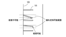
- the robot grasps the substrate 11 based on the detected distance from the substrate 11 to the substrate 11 positioned below the substrate 11. It is determined whether or not it is possible (see FIG. 7).
- the robot is gripped by correcting the motion parameters such as the robot motion position based on the detected amount of droop. .
- necessary processing such as operation stop is performed.
- the processes (2) and (3) are performed in combination.
- substrate dripping refers to a state in which the substrate housed in the cassette 10 is drooping downward from a specified position (see FIGS. 5 and 6).
- the criterion for determining whether or not the substrate 11 can be gripped by the robot can be appropriately set according to the structure of the substrate gripping mechanism of the robot.
- the imaging means 31 and the light source (illumination means) 32 are provided in the robot 30 as shown in FIG. 8 and the robot 30 is moved to the cassette 10 to be detected to detect the storage state of the substrate 11, A set of at least the imaging means 31 and the light source (illumination means) 32 is sufficient for the plurality of cassettes 10, and the apparatus can be made compact and the cost can be reduced.
- light from the light source 32 provided in the robot 30 is reflected toward the edge of the substrate 11 by the diffusion plate 33 and further reflected toward the imaging means 31 by the reflection plate 34.
- the processing of the substrate 11 is performed in an automated system, and humans do not always monitor the processing process. Therefore, when the robot 30 has an abnormality such as a conveyance failure or a collision, the cause is investigated. There was a problem that it was difficult.
- the robot 30 has caused an abnormality such as a conveyance failure or a collision.
- an abnormality such as a conveyance failure or a collision.
- the image at the time of occurrence of an abnormality can be confirmed, and the cause of the abnormality can be investigated and a recurrence prevention measure can be investigated using the image as a clue.
- an image of the cassette 10 or the like obtained by the imaging unit 31 of the substrate detection apparatus of the present invention is stored in the recording unit 35, and a past image can be referred to as necessary.
- the configuration may be such that only the latest image within the range allowed by the storage capacity of the recording means 35 is left and the old image is deleted (including overwritten).
- the configuration is such that deletion of an old image (including a case where it is overwritten) is stopped after detecting an abnormality, it is possible to avoid deleting an image for a certain period of time before the occurrence of the abnormality.
- the imaging means 31 may be provided in the robot 30 as in the second application example (see FIG. 8) or may be provided in a place other than the robot (see FIG. 9). If the image pickup means 31 is provided in the robot 30, an image representing the storage state of the wafer 11 as shown in FIG. 5 can be recorded, and the robot 30 can be operated to move to an arbitrary position from an arbitrary angle. In the latter case, the optimum imaging angle and position can be selected for investigating the cause of the abnormality and examining the recurrence prevention measures.
- Moving / rotating means for imaging means other than the robot may be provided.
- the robot 30 if the robot 30 is caused to perform a substrate transfer operation in a state where a frictional fastening portion of the robot 30 is displaced or a member is deformed due to a collision between the robot 30 and an apparatus, the robot 30 fails to transfer the substrate 11. There has been a problem of colliding with a device or the like. In addition, it is necessary to provide a dedicated detection means in order to detect the above-described deviation and deformation, which causes a problem of increasing the size and cost of the apparatus.
- image information when the robot 30 is in a specific posture during normal operation is acquired and stored in the storage means 35, and then the specific information is stored in the robot 30.
- image information when the posture is taken and comparing the obtained image information with the image information stored in the storage means 35 it is possible to detect the above-described deviation or deformation. Become.
- no dedicated detection means is required, it is possible to avoid an increase in size and cost of the apparatus.
- the image information (reference image information) when the robot 30 is in a specific posture during normal operation is acquired by the imaging unit 3 (see FIGS. 4 and 10) (see FIG. 10).
- the comparison image information and the reference image information are compared, and if there is a difference between them, it can be determined that the robot 30 is displaced or deformed.
- the comparison image information and the reference image information are shifted in the vertical direction, it is highly possible that the hand 36 is bent or the bolt is loosened.
- the cause of the abnormality of the robot 30 can also be estimated so that there is a high possibility that the robot 30 is present.
- the cause of the abnormality may be automatically estimated by a computer, or the estimation result may be displayed. Further, a threshold value may be provided for the difference between the comparison image information and the reference image information, and it may be determined that the robot 30 is displaced or deformed when the comparison result exceeds the threshold value. Further, such a determination may be performed by each element such as a vertical shift, a horizontal shift, a hand image width, or a combination thereof among the differences between the comparison image information and the reference image information.
- the operation parameters such as the operation position of the robot 30 may be corrected based on the determination result or the comparison result. In this way, even when the robot 30 is displaced or deformed, the transfer operation can be continued while the transfer operation can be performed by correcting the operation parameter, and the stop time of the apparatus can be reduced. Furthermore, if a plurality of postures are employed as the specific posture, more information can be obtained.
Landscapes
- Container, Conveyance, Adherence, Positioning, Of Wafer (AREA)
Abstract
Description
本発明の第一応用例について、図5乃至図7を参照して説明する。
(1) 本発明の基板検出装置によりカセット10内における基板11の収納状態を検出する。
(2) 基板11の飛び出し(図5参照)が検出された場合には、検出された飛び出し量に基づいてロボットによる基板11の把持が可能であるか否かの判定を行い(図6参照)、把持可能と判定された場合には、検出された飛び出し量に基づいてロボットの動作位置を補正することにより把持を行う。把持不可能と判定された場合には動作停止等の必要な処理を行う。
(3) 基板11の垂れ(図5参照)が検出された場合には、その基板11からその基板11の下方に位置する基板11までの検出された距離に基づいてロボットによる基板11の把持が可能であるか否かの判定を行い(図7参照)、把持可能と判定された場合には、検出された垂れ量に基づいてロボットの動作位置等の動作パラメータを補正することにより把持を行う。把持不可能と判定された場合には動作停止等の必要な処理を行う。
(4) 基板11の飛び出しと垂れが両方検出された場合には、(2)、(3)の処理を組合せて行う。
本発明の第二応用例について、図8を参照して説明する。
本発明の第三応用例について、図9を参照して説明する。
本発明の第四応用例について、図10(及び図4)を参照して説明する。
(1) 撮像手段3(図4、図10参照)により、正常時にロボット30に特定の姿勢をとらせた場合の画像情報(基準画像情報)を取得する(図10参照)。
(2) 取得した画像情報を記憶手段35に記憶する。
(3) ロボット30のずれや変形等を検出する際に、ロボット30に前記特定の姿勢をとらせた場合の画像情報(比較画像情報)を取得する。
(4) 比較画像情報と基準画像情報とを比較し、両者に相違がある場合にはロボット30にずれや変形等が生じていると判定できる。
Claims (14)
- カセット内に収納された複数の基板の収納状態を検出するための装置において、
前記複数の基板の傍らに配置されるコリメート反射板と、
前記コリメート反射板に向けて面状に光を放射する照明手段であって、その光路内に前記複数の基板の端部が位置するように配置される、照明手段と、
前記照明手段から面状に放射された光によって前記コリメート反射板上に形成された、前記複数の基板の端部を含む照明透過像を撮像する撮像手段と、
前記撮像手段により取得された前記照明透過像の画像を処理して、前記複数の基板の収納状態を検出する画像処理手段と、を備えた基板検出装置。 - 前記照明手段は面光源を含む請求項1記載の基板検出装置。
- 前記照明手段は、前記コリメート反射板に向けて光を放射する点光源と、前記コリメート反射板で反射されて平行化された光を、前記コリメート反射板に向けて反射する再帰反射板と、を含む請求項1記載の基板検出装置。
- 前記点光源と前記撮像手段とが互いに略同軸位置に配置されている請求項3記載の基板検出装置。
- 前記面光源又は前記点光源は発光ダイオードを含む請求項2乃至4のいずれか一項に記載の基板検出装置。
- 前記コリメート反射板は、放物線ミラーから成る請求項1乃至5のいずれか一項に記載の基板検出装置。
- 前記コリメート反射板は、複数の平面ミラーを全体として略曲面状に組み合わせて形成された曲面ミラーから成る請求項1乃至5のいずれか一項に記載の基板検出装置。
- カセット内に収納された複数の基板の収納状態を検出する方法において、
前記複数の基板の傍らに配置されたコリメート反射板に向けて、照明手段から面状の光を放射する工程であって、その光路内に前記複数の基板の端部が位置している、照明工程と、
前記照明手段から面状に放射された光によって前記コリメート反射板上に形成された、前記複数の基板の端部を含む照明透過像を撮像手段によって撮像する撮像工程と、
前記撮像手段により取得された前記照明透過像の画像を画像処理手段によって処理して、前記複数の基板の収納状態を検出する検出工程と、を備えた基板検出方法。 - 前記照明手段は面光源を含む請求項8記載の基板検出方法。
- 前記照明工程において、点光源から前記コリメート反射板に向けて光を放射し、前記コリメート反射板で反射されて平行化された光を、その光路内に前記複数の基板の端部が位置するように前記コリメート反射板に向けて再帰反射板により反射する、請求項8記載の基板検出方法。
- 前記点光源と前記撮像手段とが互いに略同軸位置に配置されている請求項10記載の基板検出方法。
- 前記面光源又は前記点光源は発光ダイオードを含む請求項9乃至11のいずれか一項に記載の基板検出方法。
- 前記コリメート反射板は、放物線ミラーから成る請求項8乃至12のいずれか一項に記載の基板検出方法。
- 前記コリメート反射板は、複数の平面ミラーを全体として略曲面状に組み合わせて形成された曲面ミラーから成る請求項8乃至12のいずれか一項に記載の基板検出方法。
Priority Applications (4)
| Application Number | Priority Date | Filing Date | Title |
|---|---|---|---|
| CN200980138891.4A CN102171806B (zh) | 2008-10-01 | 2009-09-29 | 基板检测装置及方法 |
| US13/121,498 US9202732B2 (en) | 2008-10-01 | 2009-09-29 | Apparatus and method for detecting substrates |
| EP09817767.8A EP2346072B1 (en) | 2008-10-01 | 2009-09-29 | Substrate detection device and method |
| KR1020117007656A KR101298791B1 (ko) | 2008-10-01 | 2009-09-29 | 기판검출장치 및 방법 |
Applications Claiming Priority (2)
| Application Number | Priority Date | Filing Date | Title |
|---|---|---|---|
| JP2008256268A JP5185756B2 (ja) | 2008-10-01 | 2008-10-01 | 基板検出装置および方法 |
| JP2008-256268 | 2008-10-01 |
Publications (1)
| Publication Number | Publication Date |
|---|---|
| WO2010038735A1 true WO2010038735A1 (ja) | 2010-04-08 |
Family
ID=42073496
Family Applications (1)
| Application Number | Title | Priority Date | Filing Date |
|---|---|---|---|
| PCT/JP2009/066938 Ceased WO2010038735A1 (ja) | 2008-10-01 | 2009-09-29 | 基板検出装置および方法 |
Country Status (7)
| Country | Link |
|---|---|
| US (1) | US9202732B2 (ja) |
| EP (1) | EP2346072B1 (ja) |
| JP (1) | JP5185756B2 (ja) |
| KR (1) | KR101298791B1 (ja) |
| CN (1) | CN102171806B (ja) |
| TW (1) | TWI414778B (ja) |
| WO (1) | WO2010038735A1 (ja) |
Cited By (3)
| Publication number | Priority date | Publication date | Assignee | Title |
|---|---|---|---|---|
| JP2012064918A (ja) * | 2010-08-20 | 2012-03-29 | Tokyo Electron Ltd | 基板搬送装置、基板搬送方法及びその基板搬送方法を実行させるためのプログラムを記録した記録媒体 |
| KR20120042658A (ko) * | 2010-10-22 | 2012-05-03 | 도쿄엘렉트론가부시키가이샤 | 보지 부재의 형상 판정 장치, 그 방법, 기판 처리 장치 및 기억 매체 |
| JP2014229730A (ja) * | 2013-05-22 | 2014-12-08 | 株式会社安川電機 | 基板搬送ロボット、基板搬送システムおよび基板の配置状態の検出方法 |
Families Citing this family (18)
| Publication number | Priority date | Publication date | Assignee | Title |
|---|---|---|---|---|
| JP5512350B2 (ja) * | 2010-03-30 | 2014-06-04 | 川崎重工業株式会社 | 基板搬送ロボットの状態監視装置 |
| US11880178B1 (en) | 2010-11-16 | 2024-01-23 | Ectoscan Systems, Llc | Surface data, acquisition, storage, and assessment system |
| US9599461B2 (en) | 2010-11-16 | 2017-03-21 | Ectoscan Systems, Llc | Surface data acquisition, storage, and assessment system |
| TWI484160B (zh) * | 2013-04-23 | 2015-05-11 | Au Optronics Corp | 基板檢測裝置與方法 |
| CN105206550B (zh) * | 2014-06-20 | 2018-08-24 | 北京北方华创微电子装备有限公司 | 反应腔室和半导体设备 |
| CN104916573B (zh) * | 2015-06-17 | 2018-07-06 | 北京北方华创微电子装备有限公司 | 半导体设备承载区域的硅片分布状态组合检测方法及装置 |
| KR101701419B1 (ko) * | 2016-08-17 | 2017-02-02 | 주식회사 오토닉스 | 반사형 이미지 검출 센서 |
| US10784134B2 (en) * | 2017-05-03 | 2020-09-22 | Applied Materials, Inc. | Image based substrate mapper |
| CA3084951A1 (en) | 2017-12-06 | 2019-06-13 | Ectoscan Systems, Llc | Performance scanning system and method for improving athletic performance |
| TWI641073B (zh) * | 2018-03-09 | 2018-11-11 | 創意電子股份有限公司 | 晶圓載運裝置 |
| JP7346839B2 (ja) * | 2019-02-15 | 2023-09-20 | Tdk株式会社 | ロードポート |
| JP7324667B2 (ja) | 2019-09-20 | 2023-08-10 | 株式会社Screenホールディングス | 基板処理装置 |
| JP7447661B2 (ja) * | 2020-04-23 | 2024-03-12 | Tdk株式会社 | 板状対象物の配列検出装置およびロードポート |
| US12002696B2 (en) * | 2020-06-30 | 2024-06-04 | Brooks Automation Us, Llc | Substrate mapping apparatus and method therefor |
| US11996308B2 (en) * | 2021-03-03 | 2024-05-28 | Taiwan Semiconductor Manufacturing Company, Ltd. | Method for mapping wafers in a wafer carrier |
| JP2023132455A (ja) * | 2022-03-11 | 2023-09-22 | シンフォニアテクノロジー株式会社 | 基板の検出方法及びロードポート |
| US12394647B2 (en) * | 2022-09-23 | 2025-08-19 | Taiwan Semiconductor Manufacturing Company, Ltd. | Wafer shift detection |
| TWI900052B (zh) * | 2024-06-07 | 2025-10-01 | 鏵友益科技股份有限公司 | 晶圓辨識裝置 |
Citations (5)
| Publication number | Priority date | Publication date | Assignee | Title |
|---|---|---|---|---|
| JPH09283603A (ja) * | 1996-04-10 | 1997-10-31 | Metsukusu:Kk | 半導体ウェハ検出装置 |
| JP2001093964A (ja) * | 1999-09-21 | 2001-04-06 | Nikon Corp | ウェハ検出装置 |
| JP2003017548A (ja) * | 2001-06-28 | 2003-01-17 | Sunx Ltd | ウエハ検出装置 |
| JP2005005347A (ja) | 2003-06-10 | 2005-01-06 | Yaskawa Electric Corp | 薄型基板検出方法 |
| JP2005520350A (ja) | 2000-12-01 | 2005-07-07 | ウェーハマスターズ・インコーポレイテッド | ウエハマッピング装置及び方法 |
Family Cites Families (19)
| Publication number | Priority date | Publication date | Assignee | Title |
|---|---|---|---|---|
| JPS60157230A (ja) * | 1984-01-11 | 1985-08-17 | Telmec Co Ltd | 半導体ウエハ搬送方法 |
| US4691999A (en) * | 1986-04-04 | 1987-09-08 | Hughes Aircraft Company | Afocal beam expansion apparatus and method |
| JPS63131533A (ja) * | 1986-11-21 | 1988-06-03 | Canon Inc | 斜め基板検出装置および方法 |
| JPH03239344A (ja) * | 1990-02-17 | 1991-10-24 | Kokusai Electric Co Ltd | ウェーハ検知装置 |
| US5225691A (en) * | 1992-05-18 | 1993-07-06 | Avalon Engineering, Inc. | Semiconductor wafer cassette mapper with emitter and detector arrays for slot interrogation |
| JPH06244268A (ja) * | 1993-02-16 | 1994-09-02 | Tokyo Electron Tohoku Ltd | 移載装置 |
| DE19535871C2 (de) * | 1995-09-27 | 2000-02-10 | Jenoptik Jena Gmbh | Indexer für Magazinfächer eines Magazins und darin enthaltene scheibenförmige Objekte |
| JP3977485B2 (ja) * | 1997-04-24 | 2007-09-19 | 東京エレクトロン株式会社 | アームアクセス位置検出方法及び真空処理装置 |
| DE19814046C1 (de) * | 1998-03-30 | 1999-11-18 | Jenoptik Jena Gmbh | Anordnung zur Detektion von scheibenförmigen Objekten in einer Kassette |
| JP3058615B2 (ja) * | 1998-04-10 | 2000-07-04 | 株式会社山武 | ウエハ検出装置 |
| US6914233B2 (en) * | 2001-12-12 | 2005-07-05 | Shinko Electric Co., Ltd. | Wafer mapping system |
| JP2003273197A (ja) * | 2002-03-14 | 2003-09-26 | Sunx Ltd | ウエハ飛び出し検出装置 |
| JP4163435B2 (ja) * | 2002-03-29 | 2008-10-08 | 株式会社日本マイクロニクス | 被検査基板の検査装置 |
| US20040207836A1 (en) * | 2002-09-27 | 2004-10-21 | Rajeshwar Chhibber | High dynamic range optical inspection system and method |
| JP4276440B2 (ja) * | 2003-01-06 | 2009-06-10 | 東京エレクトロン株式会社 | 基板検出方法及び装置並びに基板処理装置 |
| JP4028814B2 (ja) * | 2003-04-21 | 2007-12-26 | 川崎重工業株式会社 | マッピング装置 |
| JP2006170622A (ja) * | 2004-12-10 | 2006-06-29 | Olympus Corp | 外観検査装置 |
| WO2008100443A2 (en) | 2007-02-09 | 2008-08-21 | Bright View Technologies, Inc. | High contrast liquid crystal displays |
| AU2008323626B2 (en) * | 2007-11-15 | 2014-09-18 | Garrett Thermal Systems Limited | Particle detection |
-
2008
- 2008-10-01 JP JP2008256268A patent/JP5185756B2/ja active Active
-
2009
- 2009-09-29 WO PCT/JP2009/066938 patent/WO2010038735A1/ja not_active Ceased
- 2009-09-29 CN CN200980138891.4A patent/CN102171806B/zh active Active
- 2009-09-29 US US13/121,498 patent/US9202732B2/en active Active
- 2009-09-29 KR KR1020117007656A patent/KR101298791B1/ko active Active
- 2009-09-29 EP EP09817767.8A patent/EP2346072B1/en active Active
- 2009-10-01 TW TW098133411A patent/TWI414778B/zh active
Patent Citations (5)
| Publication number | Priority date | Publication date | Assignee | Title |
|---|---|---|---|---|
| JPH09283603A (ja) * | 1996-04-10 | 1997-10-31 | Metsukusu:Kk | 半導体ウェハ検出装置 |
| JP2001093964A (ja) * | 1999-09-21 | 2001-04-06 | Nikon Corp | ウェハ検出装置 |
| JP2005520350A (ja) | 2000-12-01 | 2005-07-07 | ウェーハマスターズ・インコーポレイテッド | ウエハマッピング装置及び方法 |
| JP2003017548A (ja) * | 2001-06-28 | 2003-01-17 | Sunx Ltd | ウエハ検出装置 |
| JP2005005347A (ja) | 2003-06-10 | 2005-01-06 | Yaskawa Electric Corp | 薄型基板検出方法 |
Non-Patent Citations (1)
| Title |
|---|
| See also references of EP2346072A4 |
Cited By (11)
| Publication number | Priority date | Publication date | Assignee | Title |
|---|---|---|---|---|
| JP2012064918A (ja) * | 2010-08-20 | 2012-03-29 | Tokyo Electron Ltd | 基板搬送装置、基板搬送方法及びその基板搬送方法を実行させるためのプログラムを記録した記録媒体 |
| US8781787B2 (en) | 2010-08-20 | 2014-07-15 | Tokyo Electron Limited | Substrate carrying mechanism, substrate carrying method and recording medium storing program including set of instructions to be executed to accomplish the substrate carrying method |
| TWI475634B (zh) * | 2010-08-20 | 2015-03-01 | 東京威力科創股份有限公司 | 基板運送裝置、基板運送方法及記錄有用來實行該基板運送方法的程式之記錄媒體 |
| CN104867856A (zh) * | 2010-08-20 | 2015-08-26 | 东京毅力科创株式会社 | 基板搬运装置、基板搬运方法和记录程序的记录介质 |
| KR101790867B1 (ko) * | 2010-08-20 | 2017-10-26 | 도쿄엘렉트론가부시키가이샤 | 기판 반송 장치, 기판 반송 방법 및 그 기판 반송 방법을 실행시키기 위한 프로그램을 기록한 기록 매체 |
| KR101891446B1 (ko) | 2010-08-20 | 2018-08-24 | 도쿄엘렉트론가부시키가이샤 | 기판 반송 장치, 기판 반송 방법 및 그 기판 반송 방법을 실행시키기 위한 프로그램을 기록한 기록 매체 |
| KR101931061B1 (ko) | 2010-08-20 | 2018-12-19 | 도쿄엘렉트론가부시키가이샤 | 기판 반송 장치, 기판 반송 방법 및 그 기판 반송 방법을 실행시키기 위한 프로그램을 기록한 기록 매체 |
| KR20120042658A (ko) * | 2010-10-22 | 2012-05-03 | 도쿄엘렉트론가부시키가이샤 | 보지 부재의 형상 판정 장치, 그 방법, 기판 처리 장치 및 기억 매체 |
| JP2012089809A (ja) * | 2010-10-22 | 2012-05-10 | Tokyo Electron Ltd | 保持部材の姿勢判定装置、その方法、基板処理装置及び記憶媒体 |
| KR101695197B1 (ko) | 2010-10-22 | 2017-01-11 | 도쿄엘렉트론가부시키가이샤 | 보지 부재의 형상 판정 장치, 그 방법, 기판 처리 장치 및 기억 매체 |
| JP2014229730A (ja) * | 2013-05-22 | 2014-12-08 | 株式会社安川電機 | 基板搬送ロボット、基板搬送システムおよび基板の配置状態の検出方法 |
Also Published As
| Publication number | Publication date |
|---|---|
| EP2346072A4 (en) | 2012-11-28 |
| US20110205354A1 (en) | 2011-08-25 |
| TW201028679A (en) | 2010-08-01 |
| CN102171806A (zh) | 2011-08-31 |
| US9202732B2 (en) | 2015-12-01 |
| KR101298791B1 (ko) | 2013-08-22 |
| CN102171806B (zh) | 2014-07-16 |
| EP2346072A1 (en) | 2011-07-20 |
| JP5185756B2 (ja) | 2013-04-17 |
| JP2010087340A (ja) | 2010-04-15 |
| EP2346072B1 (en) | 2016-05-25 |
| TWI414778B (zh) | 2013-11-11 |
| KR20110049916A (ko) | 2011-05-12 |
Similar Documents
| Publication | Publication Date | Title |
|---|---|---|
| WO2010038735A1 (ja) | 基板検出装置および方法 | |
| JP5512350B2 (ja) | 基板搬送ロボットの状態監視装置 | |
| JP5529522B2 (ja) | 基板収納状態検出装置及び基板収納状態検出方法 | |
| US8837777B2 (en) | Wafer detecting apparatus | |
| JP2011523032A (ja) | コンポーネントの表面を検出する光検出装置と方法 | |
| US20100034621A1 (en) | End effector to substrate offset detection and correction | |
| CN103033143B (zh) | 光学探测器 | |
| US20100243867A1 (en) | Mapping mechanism, foup and load port | |
| CN110914966A (zh) | 用于检查容器的方法及检查系统 | |
| CN101603926B (zh) | 多表面检测系统及方法 | |
| JP2009302392A (ja) | 基板検出装置および方法 | |
| US8379082B2 (en) | System, methods and apparatus for substrate carrier content verification using a material handling system | |
| JP3568482B2 (ja) | 板状体の傷検出方法及び装置 | |
| US7045803B2 (en) | Missing die detection | |
| KR20190134103A (ko) | 챔버에서의 결함 검사 시스템 및 그 방법 | |
| JP5387926B2 (ja) | 板状体の検出装置とケースポート及び保管装置 | |
| JP2009244175A (ja) | 測定装置の受光ユニット、姿勢検出センサの受光ユニット及びその製造方法 | |
| JP3251601U (ja) | ウェハカセット暗視装置 | |
| KR20060008201A (ko) | 광전센서 | |
| JP2021113795A (ja) | 異物検査装置 | |
| HK1169742B (en) | Wafer detecting apparatus | |
| JPH04236448A (ja) | ウェーハ用搬送アーム装置 |
Legal Events
| Date | Code | Title | Description |
|---|---|---|---|
| WWE | Wipo information: entry into national phase |
Ref document number: 200980138891.4 Country of ref document: CN |
|
| 121 | Ep: the epo has been informed by wipo that ep was designated in this application |
Ref document number: 09817767 Country of ref document: EP Kind code of ref document: A1 |
|
| WWE | Wipo information: entry into national phase |
Ref document number: 13121498 Country of ref document: US |
|
| ENP | Entry into the national phase |
Ref document number: 20117007656 Country of ref document: KR Kind code of ref document: A |
|
| NENP | Non-entry into the national phase |
Ref country code: DE |
|
| WWE | Wipo information: entry into national phase |
Ref document number: 2009817767 Country of ref document: EP |