WO2010041729A1 - 機能性デバイス及びその製造方法 - Google Patents
機能性デバイス及びその製造方法 Download PDFInfo
- Publication number
- WO2010041729A1 WO2010041729A1 PCT/JP2009/067598 JP2009067598W WO2010041729A1 WO 2010041729 A1 WO2010041729 A1 WO 2010041729A1 JP 2009067598 W JP2009067598 W JP 2009067598W WO 2010041729 A1 WO2010041729 A1 WO 2010041729A1
- Authority
- WO
- WIPO (PCT)
- Prior art keywords
- substrate
- ultraviolet curable
- curable resin
- sealing portion
- electrolyte solution
- Prior art date
- Legal status (The legal status is an assumption and is not a legal conclusion. Google has not performed a legal analysis and makes no representation as to the accuracy of the status listed.)
- Ceased
Links
Images




Classifications
-
- H—ELECTRICITY
- H01—ELECTRIC ELEMENTS
- H01G—CAPACITORS; CAPACITORS, RECTIFIERS, DETECTORS, SWITCHING DEVICES, LIGHT-SENSITIVE OR TEMPERATURE-SENSITIVE DEVICES OF THE ELECTROLYTIC TYPE
- H01G9/00—Electrolytic capacitors, rectifiers, detectors, switching devices, light-sensitive or temperature-sensitive devices; Processes of their manufacture
- H01G9/20—Light-sensitive devices
- H01G9/2027—Light-sensitive devices comprising an oxide semiconductor electrode
- H01G9/2031—Light-sensitive devices comprising an oxide semiconductor electrode comprising titanium oxide, e.g. TiO2
-
- H—ELECTRICITY
- H01—ELECTRIC ELEMENTS
- H01G—CAPACITORS; CAPACITORS, RECTIFIERS, DETECTORS, SWITCHING DEVICES, LIGHT-SENSITIVE OR TEMPERATURE-SENSITIVE DEVICES OF THE ELECTROLYTIC TYPE
- H01G9/00—Electrolytic capacitors, rectifiers, detectors, switching devices, light-sensitive or temperature-sensitive devices; Processes of their manufacture
- H01G9/20—Light-sensitive devices
- H01G9/2068—Panels or arrays of photoelectrochemical cells, e.g. photovoltaic modules based on photoelectrochemical cells
- H01G9/2077—Sealing arrangements, e.g. to prevent the leakage of the electrolyte
-
- H—ELECTRICITY
- H10—SEMICONDUCTOR DEVICES; ELECTRIC SOLID-STATE DEVICES NOT OTHERWISE PROVIDED FOR
- H10K—ORGANIC ELECTRIC SOLID-STATE DEVICES
- H10K85/00—Organic materials used in the body or electrodes of devices covered by this subclass
- H10K85/30—Coordination compounds
- H10K85/341—Transition metal complexes, e.g. Ru(II)polypyridine complexes
- H10K85/344—Transition metal complexes, e.g. Ru(II)polypyridine complexes comprising ruthenium
-
- Y—GENERAL TAGGING OF NEW TECHNOLOGICAL DEVELOPMENTS; GENERAL TAGGING OF CROSS-SECTIONAL TECHNOLOGIES SPANNING OVER SEVERAL SECTIONS OF THE IPC; TECHNICAL SUBJECTS COVERED BY FORMER USPC CROSS-REFERENCE ART COLLECTIONS [XRACs] AND DIGESTS
- Y02—TECHNOLOGIES OR APPLICATIONS FOR MITIGATION OR ADAPTATION AGAINST CLIMATE CHANGE
- Y02E—REDUCTION OF GREENHOUSE GAS [GHG] EMISSIONS, RELATED TO ENERGY GENERATION, TRANSMISSION OR DISTRIBUTION
- Y02E10/00—Energy generation through renewable energy sources
- Y02E10/50—Photovoltaic [PV] energy
- Y02E10/542—Dye sensitized solar cells
-
- Y—GENERAL TAGGING OF NEW TECHNOLOGICAL DEVELOPMENTS; GENERAL TAGGING OF CROSS-SECTIONAL TECHNOLOGIES SPANNING OVER SEVERAL SECTIONS OF THE IPC; TECHNICAL SUBJECTS COVERED BY FORMER USPC CROSS-REFERENCE ART COLLECTIONS [XRACs] AND DIGESTS
- Y02—TECHNOLOGIES OR APPLICATIONS FOR MITIGATION OR ADAPTATION AGAINST CLIMATE CHANGE
- Y02P—CLIMATE CHANGE MITIGATION TECHNOLOGIES IN THE PRODUCTION OR PROCESSING OF GOODS
- Y02P70/00—Climate change mitigation technologies in the production process for final industrial or consumer products
- Y02P70/50—Manufacturing or production processes characterised by the final manufactured product
Definitions
- the present invention relates to a functional device suitable for a dye-sensitized solar cell or the like and a manufacturing method thereof, and particularly relates to a sealing technique for a functional device.
- a solar cell is a kind of photoelectric conversion device that converts light energy into electric energy, and uses sunlight as an energy source, and therefore has a very small influence on the global environment, and is expected to be further spread.
- Dye-sensitized solar cells using photoinduced electron transfer sensitized by dyes have recently attracted attention as a next-generation solar cell that replaces silicon (Si) -based solar cells and the like and have been widely studied.
- the sensitizing dye a substance that can effectively absorb light in the vicinity of visible light, such as a ruthenium complex, is used.
- Dye-sensitized solar cells have high photoelectric conversion efficiency, do not require large-scale manufacturing equipment such as vacuum equipment, and can be manufactured easily and with high productivity using inexpensive semiconductor materials such as titanium oxide. It is expected as a solar cell of the next generation.
- a stable photoelectric conversion characteristic over a long period can be mentioned.
- a liquid electrolyte component is generally included as a constituent element.
- sealing technology is important to avoid performance degradation due to volatilization or leakage of electrolyte components, penetration of moisture, oxygen, and other components from the atmosphere into the electrolyte. It has been regarded as a difficult issue.
- Various methods for solving this problem have been studied. For example, there are the following methods.
- Patent Document 1 described later entitled “Dye-sensitized solar cell sealant” has the following description.
- the encapsulant for dye-sensitized solar cell of the invention of Patent Document 1 is a dye-sensitized solar cell in which the above two sheets are used to form a space for encapsulating an electrolyte between two opposing electrode substrates.
- a sealing material interposed between electrode substrates comprising: an electrolyte solution layer in contact with the electrolyte solution; and a gas permeable layer provided in contact with the layer, wherein the electrolyte solution layer comprises a fluoropolymer.
- the gas-resistant permeation layer is composed of at least one selected from the group consisting of polyvinylidene chloride (PVDC), ethylene-vinyl alcohol copolymer (EvOH), and polyvinyl alcohol (PVA). Take the configuration.
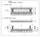
- FIG. 9 is FIGS. 1 and 2 described in Patent Document 1.
- FIG. 9A is a cross-sectional view showing an example of a dye-sensitized solar cell using a sealant for a dye-sensitized solar cell.
- FIG. 9B is a cross-sectional view showing the production process of the dye-sensitized solar cell.
- a dye-sensitized solar cell encapsulant (hereinafter abbreviated as “encapsulant”) 9 of the invention of Patent Document 1 is in contact with the electrolyte-resistant layer 107 and the electrolyte-resistant layer 107. And a gas permeation resistant layer 108 provided.
- the electrolyte solution layer 107 is configured using a fluorine-based polymer
- the gas-resistant layer 8 is configured using at least one selected from the group consisting of PVDC, EvOH, and PVA. It is a feature.
- the sealing material 109 is usually used in a mode as shown in FIG. 9A, 101 and 101 ′ are transparent substrates made of glass or the like, 102 and 102 ′ are transparent conductive films, 103 is a porous film, and 104 is a sensitizing dye. Yes, 15 is an electrolytic solution.
- the dye-sensitized solar cell shown in FIG. 9A can be manufactured as follows, for example. That is, as shown in FIG. 9B, first, a transparent conductive film 102 is formed on one surface of the transparent substrate 101, and titanium oxide particles are uniformly applied on the transparent conductive film 102 and heated. In addition, the porous film 103 is adsorbed with a sensitizing dye 104 such as a ruthenium complex to form an electrode substrate 111 serving as a cathode, and a transparent substrate 101 ′ similar to the above is formed. A transparent conductive film 102 ′ is formed on one surface, and an electrode substrate 110 serving as an anode is also configured.
- a sensitizing dye 104 such as a ruthenium complex
- the electrolytic solution layer forming composition 107 ' is applied (arranged) in a frame shape.
- a sheet (gas-resistant permeation layer 108) made of PVDC, EvOH or PVA is attached to the outer peripheral surface of the frame-shaped composition 107 ′ as shown in the figure, and the electrode substrate 111 is further shown in the figure.
- the electrode substrate 110 is opposed to each other and bonded via the frame-shaped composition 107 ′, and a sealed space is formed by both the substrates and the frame-shaped composition 107 ′. Thereafter, the composition 107 ′ is heated and vulcanized (usually 80 to 150 ° C. ⁇ 30 to 60 minutes). Then, by injecting the electrolytic solution 115 from the injection port 112 formed in the electrode substrate 110 and then closing the injection port 112, a dye-sensitized solar cell as shown in FIG. can get.
- Patent Document 2 described later entitled “Dye-sensitized solar cell module” describes that an ultraviolet curable sealing material (31X-101 manufactured by ThreeBond Co., Ltd.) is applied to the hole for electrolyte injection and cured. There is.
- an ultraviolet curable sealing material 31X-101 manufactured by ThreeBond Co., Ltd.
- JP 2007-294387 A paragraphs 0010 to 0011, paragraphs 0017 to 0018, paragraphs 0043 to 0044, FIGS. 1 and 2
- JP 2007-220606 paragraphs 0017 to 0022, paragraphs 0101 to 0102, FIGS. 1 and 2
- This outer periphery can be sealed before the liquid is injected into the gap, and since the liquid and the sealant are cured without direct contact, the cured sealant is less permeable to the liquid. If it has tolerance, a liquid can be sealed over a long period of time, and the sealing performance will be high.
- the final injection port sealing (so-called end seal) after injecting the liquid into the gap is caused by the liquid injected into the interior and the sealant before curing touching in the vicinity of the injection port. There is a problem that the adhesive strength is significantly reduced.
- the present invention has been made in order to solve the above-described problems, and its purpose is to have a high barrier characteristic and durability, and to maintain a high characteristic over a long period of time and to function stably. It is in providing a sexual device and its manufacturing method.
- the present invention provides a first substrate (for example, a photoelectrode-side transparent film in a later-described embodiment) on which a first conductive electrode (for example, a photoelectrode-side transparent conductive film 13a in a later-described embodiment) is formed.
- a second substrate for example, a counter electrode side substrate 12b in a later-described embodiment on which a substrate 12a) and a second conductive electrode (for example, a counter electrode-side conductive film 13b in a later-described embodiment) are formed.
- a functional substance for example, an electrolyte solution 16 in an embodiment described later
- a first ultraviolet curable resin A first sealing portion (for example, in an embodiment described later) that is disposed between the first substrate and the second substrate, seals the functional substance, and joins the first substrate and the second substrate.
- the inner main seal 15a) and the second A first curable resin formed of an ultraviolet curable resin, disposed between the first substrate and the second substrate, and joining the first substrate and the second substrate outside the first sealing portion;
- the present invention relates to a functional device having two sealing portions (for example, an outer main seal 17a in an embodiment described later).
- the present invention provides a first substrate (for example, a photoelectrode side transparent in an embodiment described later) on which a first conductive electrode (for example, a photoelectrode side transparent conductive film 13a in an embodiment described later) is formed.
- a first conductive electrode for example, a photoelectrode side transparent conductive film 13a in an embodiment described later
- a first step of annularly applying a first ultraviolet curable resin and a second conductive electrode for example, a counter electrode side conductive film 13b in an embodiment described later
- the second substrate (for example, the counter electrode side substrate 12b in the embodiment described later) is opposed to the first substrate, and the first ultraviolet curable resin is cured to form an annular first A second step of bonding the first substrate and the second substrate by a sealing portion (for example, an inner main seal 15a in an embodiment described later), and the outer side of the first sealing portion Between the first substrate and the second substrate A second ultraviolet curable resin is filled and cured to form a second sealing portion (for example, an outer main seal 17a in an embodiment described later), and the first substrate and the second substrate are formed.
- a sealing portion for example, an inner main seal 15a in an embodiment described later
- a third step of bonding, and an opening provided in the first substrate in an internal space formed by the first and second substrates and the first sealing portion (for example, implementation described later)
- a fourth step of filling a functional substance (for example, an electrolyte solution 16 in an embodiment to be described later) from the electrolyte solution injection holes 18a and 18b) and a fifth step of sealing the opening.
- the present invention relates to a method for manufacturing a functional device.
- an ultraviolet curable resin is formed by the first sealing portion formed between the first substrate and the second substrate and the second sealing portion formed outside the first sealing portion.
- a main seal with a double sealing structure is formed and the functional substance is sealed, so that the functional substance can be prevented from leaking to the outside and the functional substance can be shielded from the external atmosphere. It is possible to provide a functional device that has barrier characteristics, has excellent durability, maintains characteristics over a long period of time, and can operate stably.
- the first ultraviolet curable resin is annularly applied to the surface of the first substrate, the second substrate is opposed to the first substrate, and the first ultraviolet curing is performed.
- the two substrates are joined by the annular first sealing portion formed by curing the mold resin, and the second ultraviolet curable resin is filled between the substrates outside the first sealing portion.
- the second sealing portion is formed by curing, the two substrates are joined, and the opening provided in the first substrate is formed in the internal space formed by both the substrates and the first sealing portion.
- the functional material is filled from the portion, the opening is sealed, and the functional material is sealed in the internal space, the first sealing portion and the second sealing formed outside thereof As a result, a main seal having a double sealing structure made of an ultraviolet curable resin is formed, and the functional substance is sealed. While preventing leakage of the functional substance to the outside, the functional substance can be shielded from the external atmosphere, has high barrier characteristics and excellent durability, and maintains stable characteristics over a long period of time. It is possible to provide a method for manufacturing a possible functional device.
- FIG. 8 is a diagram in which the data shown in FIG. 7 is graphed. It is a figure explaining the dye-sensitized solar cell in a prior art.
- a third sealing portion that seals at least the opening and seals the functional substance, and is formed of a fourth ultraviolet curable resin, outside the third sealing portion.
- the main substance and the end seal are used to release the functional substance to the outside.
- the first ultraviolet curable resin has a low permeability of the functional substance
- the second ultraviolet curable resin has a permeability to water, oxygen, and an organic solvent. It is preferable that the functional substance is prevented from leaking to the outside and blocked from the external atmosphere by the first sealing portion and the second sealing portion. According to such a configuration, after the first ultraviolet curable resin is cured, the first ultraviolet curable resin does not decompose or denature even when it comes into contact with the functional substance. Leakage of the substance can be prevented, and the second ultraviolet curable resin has less permeability to water, oxygen, and an organic solvent after the curing than the first ultraviolet curable resin.
- the first sealing portion and the second sealing portion prevent leakage of the functional substance to the outside and form a barrier that shields it from the external atmosphere. It has excellent durability and characteristics over a long period of time. Thus, it is possible to provide a functional device that can operate stably.
- the first ultraviolet curable resin and the third ultraviolet curable resin are the same, and the second ultraviolet curable resin and the fourth ultraviolet curable resin are the same. Good. According to such a configuration, the main seal and the end seal can be formed by two different types of ultraviolet curable resins.
- the first substrate is made of a light-transmitting material and configured as a device having a photoelectric conversion function, a dimming function, or an image display function.
- a functional device such as a battery, a photosensor, or the like having a photoelectric conversion function that can photoelectrically convert incident light from the first substrate side and take it out as an electric current, or light
- a functional device such as a liquid crystal device having a dimming function capable of controlling the transmission of light, or a functional device such as an organic electroluminescence element having a color display controlled and an image display function can be realized.
- a semiconductor electrode layer formed on the surface of the first conductive electrode and holding a sensitizing dye is provided, and the electrolyte solution is filled between the first substrate and the second substrate as the functional substance.
- the dye of the sensitizing dye excited by light absorption is taken out to the semiconductor electrode layer, and the sensitizing dye that has lost the electron is reduced by the reducing agent in the electrolyte solution. It is preferable to configure as a conversion device. According to such a configuration, it is possible to realize a functional device that can photoelectrically convert incident light from the first substrate side with high conversion efficiency and take it out as an electric current.
- the fifth step is a third step of sealing the functional substance by applying and curing at least the opening with a third ultraviolet curable resin.
- Forming a sealing portion and joining a third substrate and the second substrate, and between the second substrate and the third substrate outside the third sealing portion It is preferable to include a step of filling and curing the ultraviolet curable resin 4 to form a fourth sealing portion, and joining the second substrate and the third substrate.
- the third substrate and the second substrate are joined by at least the third sealing portion that closes the opening, and the first sealing portion is outside the third sealing portion.
- the second substrate and the third substrate are joined by the fourth sealing portion, and an end seal having a double sealing structure made of an ultraviolet curable resin is formed, and the functional substance is sealed.
- the main seal and the end seal prevent leakage of the functional substance to the outside, and can block the functional substance from the external atmosphere, have high barrier properties, excellent durability, and a long period of time.
- the first ultraviolet curable resin has a low permeability of the functional substance
- the second ultraviolet curable resin has a permeability to water, oxygen, and an organic solvent. It is preferable that the functional material is prevented from leaking to the outside and blocked from the external atmosphere by the first sealing portion and the second sealing portion. According to such a configuration, after the first ultraviolet curable resin is cured, the first ultraviolet curable resin does not decompose or denature even when it comes into contact with the functional substance. Leakage of the substance can be prevented, and the second ultraviolet curable resin has less permeability to water, oxygen, and an organic solvent after the curing than the first ultraviolet curable resin.
- the first sealing portion and the second sealing portion prevent leakage of the functional substance to the outside and form a barrier that shields it from the external atmosphere. It has excellent durability and characteristics over a long period of time. Thus, it is possible to provide a method for manufacturing a functional device capable of stably operating.
- the first ultraviolet curable resin and the third ultraviolet curable resin are the same, and the second ultraviolet curable resin and the fourth ultraviolet curable resin are the same. Good. According to such a configuration, the main seal and the end seal can be formed by two different types of ultraviolet curable resins.
- the first substrate is made of a light transmissive material, and has a step of forming a semiconductor electrode layer holding a sensitizing dye on the surface of the first conductive electrode, and the functional substance is an electrolyte solution. Is filled between the first substrate and the second substrate, and the electrons of the sensitizing dye excited by light absorption are taken out to the semiconductor electrode layer, and the sensitizing dye that has lost the electrons is A dye-sensitized photoelectric conversion device that is reduced by a reducing agent in the electrolyte solution is preferably used. According to such a configuration, it is possible to realize a method for manufacturing a functional device that can photoelectrically convert incident light from the first substrate side with high conversion efficiency and extract the light as an electric current.
- the functional device of the present invention has two substrates on which conductive electrodes are formed, and the functional substance is sealed between the two substrates by shielding from the external atmosphere and sealed with an ultraviolet curable sealant having different characteristics. It has a double sealing structure.
- the functional substance is polymerized against the ultraviolet curable sealant (main sealant) used to form the inner main seal and inner end seal of the part that comes into contact with the functional substance sealed between the two substrates.
- An ultraviolet curable sealant (main sealant) is selected and used so as not to become an inhibitor, and a decrease in bonding strength between two substrates and leakage of a functional substance are prevented.
- the outer main seal and the outer end seal which are less permeable to oxygen, water, organic solvents, etc. than the inner seal, are UV curable sealant (sub sealant) outside the inner main seal and inner end seal.
- UV curable sealant sub sealant
- a functional material is sealed by a double sealing structure using an ultraviolet curable sealing agent (sealing agent) having different characteristics, and durability is provided. It became possible to fabricate functional devices with excellent performance.
- FIG. 1 is a cross-sectional view schematically showing a configuration example of a dye-sensitized solar cell in an embodiment of the present invention.
- DSC Dye-sensitized Solar Cell
- the photoelectrode is formed by a photoelectrode-side transparent conductive film 13a formed on the photoelectrode-side transparent substrate 12a.
- nano-sized titanium oxide carrying a sensitizing dye ( A TiO 2 ) semiconductor porous film 14 is formed on the photoelectrode-side transparent conductive film 13a.
- the sensitizing dye is, for example, a ruthenium bipyridyl complex.
- the counter electrode is formed by a counter electrode side conductive film 13b formed on the counter electrode side substrate 12b in which the electrolyte solution injection holes 18a and 18b are formed.
- An annular inner main sealing portion (first sealing portion) is formed so as to surround the porous film 14 by an inner main seal (sealing agent made of an ultraviolet curable adhesive) 15a on the photoelectrode side transparent conductive film 13a. ) Is formed, the photoelectrode side transparent substrate 12a and the counter electrode side substrate 12b are laminated through this inner sealing portion, and the UV curable adhesive is cured, so that the photo electrode side transparent substrate 12a and the counter electrode side substrate are cured. 12b is joined.
- An outer main seal (sealing agent made of an ultraviolet curable adhesive) 17a is injected from the periphery into the gap between the photoelectrode side transparent substrate 12a and the counter electrode side substrate 12b, and the ultraviolet curable adhesive is cured, An outer main sealing portion (second sealing portion) is formed, whereby the photoelectrode side transparent substrate 12a and the counter electrode side substrate 12b are joined outside the inner main seal 15a.
- the electrolyte solution 16 has one of the electrolyte solution injection holes 18a and 18b formed in the counter electrode side substrate 12b as an air vent hole, and from the other, the electrolyte solution 16 has both the photoelectrode side transparent substrate 12a and the counter electrode side substrate 12b. And injected into the internal space formed by the inner main seal 15a.
- An outer end seal (sealing agent made of an ultraviolet curable adhesive) 17b is injected into the gap between the counter electrode side substrate 12b and the end seal plate 19 from the peripheral portion, and the UV curable adhesive is cured, so that the counter electrode side
- the substrate 12b and the end seal plate 19 are joined to the outside of the inner end seals 15b and 15c to form an outer sub-sealing portion (fourth sealing portion).
- the electrolyte solution 16 made of a solution in which a redox system of iodine and iodine ions is dissolved in a nitrile solvent is held between the photoelectrode side transparent conductive film 13a and the counter electrode side conductive film 13b.
- the inner main seal (sealing agent) 15a, the outer main seal (sealing agent) 17a, the inner end seals 15b and 15c, and the outer end seal hold the inner space.
- the photoelectrode of the DSC When the photoelectrode of the DSC is irradiated with sunlight 11, electrons in the ground state of the sensitizing dye are excited and transition to an excited state, and the excited state electrons are between the sensitizing dye and the titanium oxide semiconductor. It is injected into the conduction band of the titanium oxide semiconductor via electrical coupling and reaches the photoelectrode.
- the sensitizing dye that has lost the electron is converted from the reducing agent in the electrolyte solution, for example, iodide ion I ⁇ to the following reaction 2I ⁇ ⁇ I 2 + 2e ⁇ . I 2 + I - ⁇ I 3 -
- an oxidant for example, triiodide ion I 3 ⁇ (a combination of I 2 and I ⁇ ) in the electrolyte solution.
- the generated oxidizing agent reaches the counter electrode by diffusion, and the reverse reaction of the above reaction I 3 ⁇ ⁇ I 2 + I ⁇ I 2 + 2e - ⁇ 2I -
- the electron is received from the counter electrode and reduced to the original reducing agent.
- Electrons sent from the transparent conductive layer to the external circuit return to the counter electrode after performing electrical work in the external circuit. In this way, light energy is converted into electrical energy without leaving any change in the sensitizing dye or the electrolyte solution. By repeating such a process, light is converted into current and electric energy is extracted to the outside.
- the photoelectrode side transparent substrate 12a a substrate having high transmittance in the visible light region, excellent barrier properties against various gases such as water and oxygen and organic solvents, and excellent in solvent resistance and weather resistance, for example, quartz,
- transparent inorganic substrates such as sapphire and glass
- transparent plastic substrates such as polyethylene terephthalate, polyethylene naphthalate, polycarbonate, polypropylene, polyphenylene sulfide, polyvinylidene fluoride, polyimide, polysulfone, and polyolefin. These can be used as the counter electrode side substrate 12 b and the end seal plate 19.
- the photoelectrode-side transparent conductive film 13a for example, indium-tin composite oxide (ITO), fluorine-doped SnO 2 (FTO), antimony-doped SnO 2 (ATO), SnO 2 or the like can be used.
- ITO indium-tin composite oxide
- FTO fluorine-doped SnO 2
- ATO antimony-doped SnO 2
- the semiconductor material constituting the semiconductor porous film 14 is preferably an n-type semiconductor material in which conduction band electrons become carriers under photoexcitation to generate an anode current, and anatase-type titanium oxide TiO 2 is preferable.
- anatase-type titanium oxide TiO 2 is preferable.
- MgO, ZnO, SnO 2, WO 3, Fe 2 O 3, In 2 O 3, Bi 2 O 3, Nb 2 O 5, SrTiO 3, BaTiO 3, ZnS, CdS, CdSe, CdTe, PbS, CuInS InP or the like can be used.
- sensitizing dye supported on the semiconductor fine particles those formed by complexing with a metal such as ruthenium (Ru), zinc (Zn), platinum (Pt), palladium (Pd) can be used. High quantum yield is particularly preferable.
- Other dyes such as xanthene dyes, cyanine dyes, porphyrin dyes, anthraquinone dyes, polycyclic quinone dyes, and the like can be used as long as they provide a sensitizing action.
- the electrolyte solution 16 is a solution in which a redox system (redox pair) that reversibly changes state of oxidation / reduction is dissolved in a solvent.
- Redox couples include, for example, halogens such as I ⁇ / I 3 ⁇ and Br ⁇ / Br 2 , pseudohalogens such as quinone / hydroquinone and SCN ⁇ / (SCN) 2 , iron (II) ions / iron (III) Ions, copper (I) ions / copper (II) ions, and the like.
- a combination of iodine (I 2 ) and metal iodide or organic iodide, or a combination of bromine (Br 2 ) and metal bromide or organic bromide can be used as the electrolyte.
- the cations constituting the metal halide salt are Li + , Na + , K + , Cs + , Mg 2 + , Ca 2 + and the like.
- the cations constituting the organic halide salt are tetraalkylammonium ions, pyridinium. Quaternary ammonium ions such as ions and imidazolium ions are preferred.
- a combination of ferrocyanate and ferricyanate, a combination of ferrocene and ferricinium ion, a sodium polysulfide or a combination of alkylthiol and alkyl disulfide can be used as the electrolyte.
- an electrolyte combining iodine (I 2 ) and imidazolium compounds such as lithium iodide (LiI), sodium iodide (NaI), or imidazolium iodide is preferable.
- water, various organic solvents, and ionic liquid can be used as the solvent of the electrolyte solution 16. More specifically, for example, nitriles such as acetonitrile, carbonates such as propylene carbonate and ethylene carbonate, gamma butyrolactone, pyridine, dimethylacetamide, other polar solvents, and ionic properties such as methylpropylimidazolium-iodine (MPII) Liquids or mixtures thereof can be used.
- nitriles such as acetonitrile
- carbonates such as propylene carbonate and ethylene carbonate
- gamma butyrolactone gamma butyrolactone
- pyridine dimethylacetamide
- dimethylacetamide other polar solvents
- ionic properties such as methylpropylimidazolium-iodine (MPII) Liquids or mixtures thereof can be used.
- MPII methylpropylimidazolium
- An additive may be added for the purpose of preventing reverse electron transfer in the electrolyte solution and improving the open-circuit voltage and the short-circuit current.
- this additive tert-butylpyridine, 1-methoxybenzimidazole, carboxylic acid having a long-chain alkyl group having about 13 carbon atoms, or the like is used.
- an inorganic salt such as lithium iodide or sodium iodide, or a molten salt such as imidazolium or quaternary ammonium may be added to the electrolyte solution as a supporting electrolyte.
- the counter electrode-side conductive film 13b is desirably electrochemically stable.
- platinum, gold, carbon, conductive polymer, or the like can be used.
- the inner main seal 15a and inner end seals 15b and 15c are denatured even if they come into contact with the electrolyte solution 16 before and after curing in order to suppress deterioration of the electrolyte solution 16 and sensitizing dye due to high temperature exposure during curing of the sealing resin.
- an ultraviolet curable resin adheresive
- it is more desirable that the permeability of the electrolyte solution 16 to the solvent, water, and oxygen after curing is small.
- an ultraviolet curable resin (adhesive) (which can be cured at a low temperature) different from the inner main seal 15a and the inner end seals 15b and 15c is used.
- the outer main seal 17a and the outer end seal 17b are less permeable to water, oxygen, and organic solvent than the inner main seal 15a and the inner end seals 15b and 15c after being cured.
- the width of the outer main seal 17a is larger than the width of the inner main seal 15a so that the outer main seal 17a effectively acts as a barrier against permeation of water, oxygen and organic solvents.
- the width of the seal is a dimension in a direction parallel to the surfaces of the substrates 12a and 12b.
- the inner main seal 15a and inner end seals 15b and 15c having good iodine resistance are prevented from being deteriorated by using the inner main seal 15a and inner end seals 15b and 15c with good iodine resistance as in the sealing structure described above.
- leakage of the electrolyte and solvent of the electrolyte solution 16 can be suppressed, and intrusion of water and oxygen from the atmosphere into the electrolyte solution 16 can be suppressed, so that the performance of the DSC can be maintained and the life can be extended. be able to.
- the inner main seal 15a and the inner end seals 15b and 15c may be different ultraviolet curable resins (adhesives). Further, if the outer main seal 17a and the outer end seal 17b are different in UV curable resin (adhesive) as long as it has less water, oxygen, and organic solvent permeability than the inner main seal 15a and the inner end seals 15b and 15c, ).
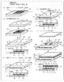
- FIG. 2 is a perspective view for explaining an example of the manufacturing process of the dye-sensitized solar cell in the embodiment of the present invention, and a diagram including an SS section sectional view.
- the manufacturing process of the dye-sensitized solar cell includes (A), (B, (C), (D), and (E).
- a photomask is formed on the photoelectrode-side transparent conductive film 13a so as to surround the TiO 2 porous film 14 carrying the sensitizing dye, and the inner main seal (inner Main sealant) 15a is applied in a ring shape.
- the counter electrode side substrate 12b and the photoelectrode side transparent substrate 12a are overlapped via the inner main seal 15a so that the conductive films 13a and 13b formed thereon are opposed to each other.
- the inner main seal 15a is cured by irradiating ultraviolet rays, and both the substrates 12a and 12b are bonded.
- an outer main seal (outer main sealant) 17a having a low viscosity is injected into the gap between the peripheral portions of the joined substrates 12a and 12b using capillary action.
- the two substrates 12a and 12b are bonded at the peripheral edge by irradiating and curing ultraviolet rays.
- an internal space having an opening having electrolyte solution injection holes 18a and 18b is formed by both the substrates 12a and 12b and the inner main seal 15a.
- one of the electrolyte solution injection holes 18a and 18b is used as an air vent hole, and the electrolyte solution 16 containing iodine or the like is injected into the internal space from the other hole.
- an inner end seal (inner auxiliary sealant) is formed so that a photomask is formed on the counter electrode side substrate 12b and at least the openings of the electrolyte solution injection holes 18a and 18b are closed. ) Apply 15b and 15c.
- the inner end seals 15b and 15c may be connected.
- the end seal plate 19 is overlapped on the counter electrode side substrate 12 through the inner end seals 15b and 15c, and the inner end seals 15b and 15c are cured by irradiating ultraviolet rays, so that the counter electrode side substrate 12 and the end seal are cured.
- the plates 19 are joined.
- an outer end seal (outer subsealing agent) 17b having a low viscosity is injected into the gap between the bonded counter electrode side substrate 12 and the peripheral edge of the end seal plate 19 by utilizing capillary action, and ultraviolet rays are injected.
- the counter electrode side substrate 12 and the end seal plate 19 are joined at the peripheral edge portion by irradiation and curing.
- the end seal plate 19 is joined to the counter electrode side substrate 12b by the inner end seals 15b and 15c and the outer end seal 17b, the electrolyte solution injection holes 18a and 18b are sealed, and the electrolyte solution 16 is added to the lower atmosphere. And is sealed in the internal space.
- the inner main seal 15a and the inner end seals 15b and 15c are not denatured even when they come into contact with the electrolyte solution 16 before and after curing, the bonding strength does not decrease after curing, and the iodine resistance is good. It is preferable to use an ultraviolet curable resin (adhesive) having low properties, and it is more desirable that the electrolyte solution 16 has less permeability to the electrolyte, solvent, water, and oxygen after curing.
- an ultraviolet curable resin (adhesive) different from the inner main seal 15a and the inner end seals 15b and 15c is used as the outer main seal 17a and the outer end seal 17b.
- the outer main seal 17a and the outer end seal 17b are less permeable to water, oxygen, and organic solvent than the inner main seal 15a and the inner end seals 15b and 15c after being cured.
- the inner main seal 15a and the inner end seals 15b and 15c may be different ultraviolet curable resins (adhesives). Further, if the outer main seal 17a and the outer end seal 17b are different in UV curable resin (adhesive) as long as it has less water, oxygen, and organic solvent permeability than the inner main seal 15a and the inner end seals 15b and 15c, ).
- the ultraviolet curable sealant (main seal) used for forming the inner main seal 15a and the inner end seals 15b and 15c at the portion in contact with the electrolyte solution 16 is used.
- an ultraviolet curable sealant (main sealant) is selected and used so that components contained in the electrolyte solution 16, such as iodine, do not become polymerization inhibitors. Leakage of the electrolyte solution 16 is prevented.
- the outer main seal 17a and the outer end seal 17b which are less permeable to water, oxygen, organic solvents and the like than the inner seal, are located outside the inner main seal 15a and the inner end seals 15b and 15c. Formed by an ultraviolet curable sealant (sub-sealant), leakage of the solvent of the electrolyte solution 16 is prevented, and water, oxygen, etc. enter from the external atmosphere into the internal space where the electrolyte solution 16 is sealed Is prevented.
- the DSC according to the present embodiment has iodine resistance as an ultraviolet curable sealing resin for the inner seal that forms the inner seals 15 a, 15 b, and 15 c in contact with the electrolyte solution 16.
- a resin having low iodine permeability is used.
- an ultraviolet curable sealing resin for outer seals that forms outer seals 17a and 17b that do not come into contact with the electrolyte solution 16
- it has water resistance, oxygen resistance, and organic solvent resistance, and is permeable to water, oxygen, and organic solvents. Less resin is used.
- the electrolyte solution 16 is sealed by using an ultraviolet curable sealant (sealant) having different characteristics to provide durability.
- an ultraviolet curable sealant silant
- a DSC having excellent durability can be manufactured in accordance with the use environment and resistance.
- This embodiment mode is not limited to DSC, and has two substrates on which conductive electrodes are formed. A functional substance is shielded from the external atmosphere and sealed between the two substrates, and has characteristics over a long period of time.
- Functional devices required to be maintained for example, photoelectric conversion devices other than DSC (for example, optical sensors), chemical batteries, organic and inorganic electroluminescent elements, display devices using organic or inorganic electroluminescent elements, biosensors, capacitors
- the present invention can also be applied.
- Titanium oxide was applied on the FTO layer of the photoelectrode with a screen printing machine and sintered at 510 ° C. for 30 minutes to form a titanium oxide (TiO 2 ) semiconductor porous film 14 as a semiconductor porous film.
- FIG. 3 is a diagram showing examples of sensitizing dyes in Examples of the present invention.
- ruthenium (II) tri-tetrabutylammonium complex (manufactured by Solaronix) shown in FIG. , Ru 620-1H3TBA) (black dye, commonly referred to as N749).
- This dye has a peak of absorption in the vicinity of visible light (600 nm) and is a typical sensitizing dye of a dye-sensitized solar cell in which absorption spreads to 800 nm (near infrared).
- TBA in FIG. 3 is tetrabutylammonium (tetrabuthylammonium) (N ((CH 2 ) 3 CH 3 ) 4 ).
- Counter electrode As a counter electrode in which the counter electrode side conductive film 13b is formed on the counter electrode side substrate 12b, glass / Cr / Pt (Co., Ltd.) in which Cr (thickness: 500 mm) / Pt (thickness: 1000 mm) is sputtered on a glass plate, respectively. Purchased from Geomatek.).
- a photomask is formed on the photoelectrode-side transparent conductive film 13a so as to surround the TiO 2 porous film 14 carrying the sensitizing dye, and an ultraviolet curable resin is formed.
- the counter electrode side substrate 12b and the photoelectrode side transparent substrate 12a are overlapped via the inner main seal 15a so that the conductive films 13a and 13b formed thereon are opposed to each other.
- the inner main seal 15a was cured by irradiating ultraviolet rays, and both the substrates 12a and 12b were joined.
- an ultraviolet curable resin having a low viscosity (TB3042, manufactured by ThreeBond Co., Ltd., a one-component non-solvent radical curable resin) is formed in the gap between the peripheral portions of the bonded substrates 12a and 12b.
- an outer main seal (outer main sealant) 17a which was injected by utilizing a capillary phenomenon, and cured by irradiating with ultraviolet rays to bond both substrates 12a and 12b at the peripheral edge.
- an internal space in which the electrolyte solution 16 was enclosed was formed by the two substrates 12a and 12b and the inner main seal 15a.
- one of the electrolyte solution injection holes 18a and 18b formed in the counter electrode substrate 12b is an air vent hole, and the electrolyte solution 16 containing iodine or the like is extracted from the other hole. Injected into the interior space.
- FIG. 4 is a diagram showing an example of the composition of the electrolyte solution in the example of the present invention.
- the electrolyte solution 16 having the layer shown in FIG. 4 was injected into the internal space from one of the electrolyte solution injection holes 18a and 18b.
- DMPImI shown in FIG. 4 is 1,2-dimethyl-3-propyl-1H-imidazole-3-iumiodide (1,2-dimethyl-3-propyl-1H-imidazole-3-iumiodide) ( C 8 H 15 N 2 ).
- the end seal plate 19 is overlapped on the counter electrode side substrate 12 through the inner end seals 15b and 15c, and the inner end seals 15b and 15c are cured by irradiating ultraviolet rays, so that the counter electrode side substrate 12 and the end seal are cured.
- the plate 19 was joined.
- an ultraviolet curable resin having a low viscosity (TB3042, manufactured by Three Bond Co., Ltd.) is placed outside in the gap between the bonded counter electrode side substrate 12 and the peripheral edge of the end seal plate 19. This was injected as an end seal (outer main sealant) 17b using a capillary phenomenon, cured by irradiating with ultraviolet rays, and the counter electrode side substrate 12 and the end seal plate 19 were joined at the peripheral edge.
- the end seal plate 19 is joined to the counter electrode side substrate 12b by the inner end seals 15b and 15c and the outer end seal 17b, the electrolyte solution injection holes 18a and 18b are sealed, and the electrolyte solution 16 is added to the lower atmosphere. And was sealed in the internal space.
- the above-mentioned ultraviolet curable resin TB3042 (manufactured by ThreeBond Co., Ltd.) was cured by ultraviolet rays even in the presence of iodine, and could be cured even in contact with the electrolyte solution 16 containing iodine.
- the above-described ultraviolet curable resin TB3042 (manufactured by ThreeBond Co., Ltd.) is superior in water resistance and oxygen resistance than the 31X-101 series resin, and has a lower viscosity than the 31X-101 series resin. It was possible to easily enter the narrow gap by capillary action.
- an ultraviolet curable sealant (main sealant, 31X-101 series resin) used for forming the inner main seal 15a and the inner end seals 15b and 15c at the portion in contact with the electrolyte solution 16 is used.
- the iodine contained in the electrolyte solution 16 was not a polymerization inhibitor, and it was possible to prevent a decrease in bonding strength and leakage of the electrolyte solution 16.
- the outer main seal 17a and the outer end seal 17b which are superior to the main sealant (31X-101 series resin) in water resistance and oxygen resistance, are placed outside the inner main seal 15a and the inner end seals 15b and 15c. Since it is formed by the sealing agent (TB3042), leakage of iodine and organic solvent constituting the electrolyte solution 16 is prevented, and intrusion of water, oxygen, etc. from the external atmosphere to the internal space where the electrolyte solution 16 is sealed is prevented. It was possible to prevent this, maintain the photoelectric conversion efficiency for a long time, and improve the durability.
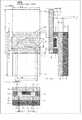
- FIG. 5 is a diagram showing a configuration example of a dye-sensitized solar cell in an example of the present invention, in which FIG. 5A is a plan view, FIG. 5B is a cross-sectional view taken along line AA, FIG. 5C is a cross-sectional view taken along the line BB.
- FIG. 5 shows the structure and dimensions of the dye-sensitized solar cell manufactured by the embodiment described above.
- the photoelectrode-side transparent substrate 12a and the counter electrode-side substrate 12b are not oppositely bonded to each other.
- the photoelectrode-side conductive film 13a and the counter-electrode-side conductive film 13b are exposed to the outside.
- the external terminal is connected to this portion, and the current generated by the DSC is taken out to the outside.
- the width of the inner main seal 15a is 1 mm
- the width of the outer main seal 17a is 1.5 mm
- the width of the outer main seal 17a is larger than the width of the inner main seal 15a
- the outer main seal 17a has water, oxygen, It acts effectively as a barrier against permeation of organic solvents.
- the width of the seal is a dimension in a direction parallel to the surfaces of the substrates 12a and 12b.
- the opening diameter of the electrolyte solution injection holes 18a and 18b is 0.3 mm ⁇ although not shown in FIG.
- the end seal plate 19 is made of a glass plate with low permeability, and the end seals 15b, 15c, and 17b are sandwiched between the counter electrode side substrate 12b and the end seal plate 19 and leak in a direction perpendicular to the counter electrode side substrate 12b. Is prevented by the end seal plate 19.
- Comparative example As described above, the DSC formed by the main seal and end seal of the double sealing structure with different ultraviolet curable resins is formed by the main seal and end seal of the double sealing structure with a single ultraviolet curable resin. In order to confirm that the DSC was superior to the formed DSC, a comparative example was manufactured, a characteristic deterioration evaluation experiment was performed, and the durability was compared with the DSC according to the example.
- the ultraviolet curable sealant (main sealant (31X-101 series resin, manufactured by ThreeBond)) is represented as ⁇ , and the ultraviolet curable sealant (sub-encapsulant (TB3042, manufactured by ThreeBond) is used. )) Is represented as ⁇ .
- FIG. 6 is a diagram showing an example of the sealing structure of the dye-sensitized solar cell in the example of the present invention.
- FIG. 6 (A) is a (double main seal + double end seal) structure, (B) is a (double main seal + 1 double end seal) structure, and (C) is (single main seal + double end seal). Structure, (D) shows (single main seal + double end seal) structure, (A) is a double sealing structure in the embodiment shown above, (B), (C), (D) are comparisons The sealing structure in an example is shown.
- the main seal has a double sealing structure of ⁇ and ⁇ , the inner seal 15a is formed of ⁇ , and the outer seal 17a is formed of ⁇ . ing.
- the main seal has a single sealing structure with ⁇ , and the inner seal 15a and the outer seal 17a are formed with ⁇ .
- the end seal has a double sealing structure of ⁇ and ⁇ , the inner seals 15b and 15c are formed of ⁇ , and the outer seal 17b is formed of ⁇ . Forming.
- the end seal has a single sealing structure by ⁇ , and the inner seals 15b and 15c and the outer seal 17b are formed by ⁇ .
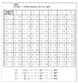
- FIG. 7 is a diagram showing the relationship between the sealing structure shown in FIG. 6 and the characteristic deterioration of the dye-sensitized solar cell.
- FIG. 7 (A) -1, (A) -2, and (A) -3 are (double main seal + double end seal) structure shown in FIG. 6, (B) -1, (B)- 2 shows the structure shown in FIG. 6 (double main seal + 1 double end seal), and (C) -1, (C) -2, and (C) -3 show FIG. 6 (single main seal + double end seal). Structures (D) -1, (D) -2, and (D) -3 respectively show the (single main seal + 1 double end seal) structure shown in FIG.
- the open-circuit voltage (V oc ) and short-circuit current of the I (current) -V (voltage) curve when irradiated with simulated sunlight (AM1.5, 100 mW / cm 2 ) (J sc ), fill factor (ff) and photoelectric conversion efficiency were measured.
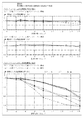
- FIG. 8 is a graph of the data shown in FIG. 7.
- FIG. 8 (1) shows a case where the main seal has a double sealing structure of ⁇ and ⁇
- FIG. 8 (2) shows that the main seal is ⁇ .
- the case of the single sealing structure by is shown.
- FIG. 8 In (1) of FIG. 8, (A) shows the data of (A) -1, (A) -2, (A) -3 in FIG. 7, and (B) shows (B) -1, (B) -2 data is shown. 8 (2), (C) shows data of (C) -1, (C) -2, (C) -3 in FIG. 7, and (D) shows (D)-in FIG. Data of 1, (D) -2, (D) -3 are shown.
- the main seal shows almost no characteristic deterioration in the double sealing structure due to ⁇ and ⁇ .
- the characteristic deterioration in the single-sealed structure due to is significantly increased when the number of elapsed days exceeds three days.
- the characteristic deterioration of the single seal structure due to the ⁇ only in the main seal is remarkable.
- iodine resistance is required for the main seal having a large area in contact with the electrolyte solution and a short distance from the electrolyte solution to the external atmosphere. It has been shown that a sealed structure having only ⁇ cannot prevent deterioration of characteristics caused by permeation and penetration of an organic solvent such as acetonitrile, water, and oxygen.
- this double sealing structure is added to the ⁇ sealing structure with iodine resistance. It is considered that the sealed structure by ⁇ suppresses permeation and penetration of organic solvents such as acetonitrile, water, oxygen and the like, and contributes notably to the deterioration of characteristics.
- ⁇ has a shielding property against an electrolyte solution component (assumed to be methoxyacetonitrile in view of the contained amount) rather than water / oxygen resistance. Because of the large size, it is considered that the difference in characteristics due to the sealing structure of the end seal in (A) and (B) of (1) in FIG. 8 is hardly seen.
- an ultraviolet curable sealant (main sealant (i.e., main sealant) having iodine resistance is used to form the inner seals 15a, 15b, and 15c at the portions in contact with the electrolyte solution 16. 31X-101 series resin)) and UV curable sealant (sub-sealant (TB3042)) which has better water resistance, oxygen resistance and mechanical strength than inner seals 15a, 15b and 15c. ),
- main sealant i.e., main sealant having iodine resistance
- sub-sealant sub-sealant
- the materials of the substrates 12 a and 12 b and the end seal substrate 19, the materials of the conductive films 13 a and 13 b, the type of the sensitizing dye, the material of the porous film 1, and the composition of the electrolyte solution 16 used for a functional device such as DSC. can be arbitrarily changed as necessary.
- the UV curable sealing resin for the inner seal that forms the inner seals 15a, 15b, and 15c that contacts the electrolyte solution 16 has iodine resistance, and the outer that forms the outer seals 17a and 17b that do not contact the electrolyte solution 16. If the ultraviolet curable sealing resin for sealing has water resistance, oxygen resistance, and organic solvent resistance, it can be used as appropriate.
- the present invention can provide a functional device such as a dye-sensitized solar cell that has good sealing performance and can maintain high efficiency for a long time.
Landscapes
- Engineering & Computer Science (AREA)
- Power Engineering (AREA)
- Chemical & Material Sciences (AREA)
- Chemical Kinetics & Catalysis (AREA)
- Electrochemistry (AREA)
- Microelectronics & Electronic Packaging (AREA)
- Hybrid Cells (AREA)
- Photovoltaic Devices (AREA)
Abstract
Description
[色素増感太陽電池の構成例]
図1は、本発明の実施の形態における、色素増感太陽電池の構成例を模式的に示す断面図である。
2I- → I2 +2e-
I2 + I- →I3 -
によって電子を受け取り、電解質溶液中に酸化剤、例えば、三ヨウ化物イオンI3 -(I2 とI-との結合体)を生成させる。生じた酸化剤は拡散によって対向電極に到達し、上記反応の逆反応
I3 - → I2 +I-
I2 +2e- →2I-
によって対向電極から電子を受け取り、もとの還元剤に還元される。
図2は、本発明の実施の形態における、色素増感太陽電池の製造工程の例を説明する斜視図、SS部断面図を含む図である。
以下、色素増感太陽電池の封止構造について説明する。図2に示す製造工程に従って色素増感太陽電池を製作した。
ガラス板からなる光電極側透明基板12aと、その上にFTO材料が透明導電膜として形成された光電極側透明電導膜13aからなる光電極として、日本板硝子社製FTO材料(10Ω)を使用した。
上記の光電極のFTO層上にスクリーン印刷機で酸化チタンを塗布し、510℃にて30分焼結して、半導体多孔質膜として酸化チタン(TiO2)半導体多孔質膜14を形成した。
図3は、本発明の実施例における、増感色素の例を示す図である。
対向電極側電導膜13bが対向極側基板12b上に形成された対向電極として、ガラス板にCr(厚さ500Å)/Pt(厚さ1000Å)がそれぞれスパッタされたガラス/Cr/Pt(株式会社ジオマテックより購入。)を使用した。
図2の(A)に示すように、増感色素が担持されたTiO2多孔質膜14を包囲するように、光電極側透明導電膜13a上にフォトマスクを形成して、紫外線硬化型樹脂(スリーボンド社製、31X-101系樹脂、メタアクリレート基を有するポリブタジエン重合材)を内側メインシール(内側主封止剤)15aとして使用してこれを環状に塗布した。
図2の(C)に示すように、接合された両基板12a、12bの周縁部の間隙に、粘度の小さい紫外線硬化型樹脂(スリーボンド社製、TB3042、一液性無溶剤のラジカル硬化型樹脂)を外側メインシール(外側主封止剤)17aとしてこれを、毛細管現象を利用して注入し、紫外線を照射して硬化させて上記の周縁部で両基板12a、12bを接合した。この結果、両基板12a、12bと内側メインシール15aによって、電解質溶液16が封入される内部空間が形成された。
図2の(D)に示すように、対向極側基板12bに形成されている電解質溶液用注入孔18a、18bの一方を空気抜き孔とし他方の孔から、ヨウ素等を含む電解質溶液16を、上記の内部空間に注入した。
図2の(E)に示すように、対向電極側基板12b上にフォトマスクを形成して電解質溶液用注入孔18a、18bの開口部を少なくとも塞ぐように、紫外線硬化型樹脂(スリーボンド社製、31X-101系樹脂)を内側エンドシール(内側副封止剤)15b、15cとして使用してこれを塗布した。なお、この内側エンドシール15b、15cは、図2に示す例とは異なり、連接して形成した。
次に、図2の(E)に示すように、接合された対向電極側基板12とエンドシール板19の周縁部の間隙に、粘度の小さい紫外線硬化型樹脂(スリーボンド社製、TB3042)を外側エンドシール(外側主封止剤)17bとしてこれを、毛細管現象を利用して注入し、紫外線を照射して硬化させて上記の周縁部で対向電極側基板12とエンドシール板19を接合した。
図5は、本発明の実施例における、色素増感太陽電池の構成例を示す図であり、図5の(A)は平面図、図5の(B)はA-A部断面図、図5の(C)はB-B部断面図である。
以上説明したような、異なる紫外線硬化型樹脂による2重封止構造のメインシール及びエンドシールによって形成されたDSCが、単一の紫外線硬化型樹脂による2重封止構造のメインシール及びエンドシールによって形成されたDSCよりも、優れていることを確認するために比較例を製作し、特性劣化評価実験を行い、実施例によるDSCとの耐久性の比較を行った。
以下の説明では、紫外線硬化型封止剤(主封止剤(31X-101系樹脂、スリーボンド社製))をαと表し、紫外線硬化型封止剤(副封止剤(TB3042、スリーボンド社製))をβと表すことにする。
図7は、図6に示す封止構造と色素増感太陽電池の特性劣化の関係を示す図である。図7において、特性劣化は、初回の光電変換効率の測定時点(経過日数=0日とする。)から経過日数と、この経過日数後に実測された光電変換効率を、初回に測定された光電変換効率で規格化して得られた光電変換効率(%、相対光電変換効率)によって、示している。
Claims (11)
- 第1の導電性電極が形成された第1の基板と、
第2の導電性電極が形成された第2の基板と、
前記第1の基板と前記第2の基板の間に充填された機能物質と、
第1の紫外線硬化型樹脂によって形成され、前記第1の基板と前記第2の基板の間に配置され、前記機能物質を封止し前記第1の基板と前記第2の基板を接合する第1の封止部と、
第2の紫外線硬化型樹脂によって形成され、前記第1の基板と前記第2の基板の間に配置され、前記第1の封止部の外側で前記第1の基板と前記第2の基板を接合する第2の封止部と、
を有する機能性デバイス。 - 前記第2の基板に形成され、前記第1の基板と前記第2の基板の間に前記機能物質を充填するための開口部と、第3の紫外線硬化型樹脂によって形成され、少なくとも前記開口部を塞ぐように形成され前記機能物質を封止する第3の封止部と、第4の紫外線硬化型樹脂によって形成され、前記第3の封止部の外側に配置された第4の封止部と、前記第3の封止部と前記第4の封止部によって前記第2の基板に接合された第3の基板とを有する、請求項1に記載の機能性デバイス。
- 前記第1の紫外線硬化型樹脂は、前記機能物質の透過性が少なく、前記第2の紫外線硬化型樹脂は、水、酸素、有機溶媒に対する透過性が、前記第1の紫外線硬化型樹脂よりもさく、前記第1の封止部及び前記第2の封止部によって、前記機能物質の外部への漏洩が防止され、外部の雰囲気から遮断された、請求項1又は請求項2に記載の機能性デバイス。
- 前記第1の紫外線硬化型樹脂と前記第3の紫外線硬化型樹脂が同じであり、前記第2の紫外線硬化型樹脂と前記第4の紫外線硬化型樹脂が同じである、請求項3に記載の機能性デバイス。
- 前記第1の基板が光透過性の材料からなり、光電変換機能、又は、調光機能、又は、画像表示機能を有するデバイスとして構成された、請求項3に記載の機能性デバイス。
- 光電変換機能として構成された機能性デバイスであり、前記第1の導電性電極の面に形成され増感色素を保持した半導体電極層を有し、前記機能物質として、電解質溶液が前記第1の基板と前記第2の基板の間に充填され、光吸収によって励起された前記増感色素の電子が前記半導体電極層へ取り出されるとともに、前記電子を失った前記増感色素が、前記電解質溶液中の還元剤によって還元される色素増感光電変換装置として構成された、請求項5に記載の機能性デバイス。
- 第1の導電性電極が形成された第1の基板の面に、第1の紫外線硬化型樹脂を環状に塗布する第1の工程と、
第2の導電性電極が形成された第2の基板を前記第1の基板に対向させ、前記第1の紫外線硬化型樹脂を硬化させて形成された環状の第1の封止部よって、前記第1の基板と前記第2の基板を接合する第2の工程と、
前記第1の封止部の外側において前記第1の基板と前記第2の基板の間に、第2の紫外線硬化型樹脂を充填して硬化させて第2の封止部を形成し、前記第1の基板と前記第2の基板を接合する第3の工程と、
前記第1及び第2の基板と前記第1の封止部によって形成された内部空間に、前記第1の基板に設けられている開口部から機能物質を充填する第4の工程と、
前記開口部を封止する第5の工程と
を有する機能性デバイスの製造方法。 - 前記第5の工程は、第3の紫外線硬化型樹脂によって少なくとも前記開口部を塞ぐように塗布して硬化させて、前記機能物質を封止する第3の封止部を形成し、第3の基板と前記第2の基板を接合する工程と、前記第3の封止部の外側において前記第2の基板と前記第3の基板の間に、第4の紫外線硬化型樹脂を充填して硬化させて第4の封止部を形成し、前記第2の基板と前記第3の基板を接合する工程を有する、請求項7に記載の機能性デバイスの製造方法。
- 前記第1の紫外線硬化型樹脂は、前記機能物質の透過性が少なく、前記第2の紫外線硬化型樹脂は、水、酸素、有機溶媒に対する透過性が、前記第1の紫外線硬化型樹脂よりもさく、前記第1の封止部及び前記第2の封止部によって、前記機能物質の外部への漏洩が防止され、外部の雰囲気から遮断される、請求項7又は請求項8に記載の機能性デバイスの製造方法。
- 前記第1の紫外線硬化型樹脂と前記第3の紫外線硬化型樹脂が同じであり、前記第2の紫外線硬化型樹脂と前記第4の紫外線硬化型樹脂が同じである、請求項9に記載の機能性デバイスの製造方法。
- 前記第1の基板が光透過性の材料からなり、増感色素を保持した半導体電極層を前記第1の導電性電極の面に形成する工程を有し、前記機能物質として、電解質溶液が前記第1の基板と前記第2の基板の間に充填され、光吸収によって励起された前記増感色素の電子が前記半導体電極層へ取り出されるとともに、前記電子を失った前記増感色素が、前記電解質溶液中の還元剤によって還元される色素増感光電変換装置として構成された、請求項7又は請求項8に記載の機能性デバイスの製造方法。
Priority Applications (4)
| Application Number | Priority Date | Filing Date | Title |
|---|---|---|---|
| CN2009801012925A CN101889366A (zh) | 2008-10-09 | 2009-10-09 | 功能性器件及其制造方法 |
| BRPI0906022-7A BRPI0906022A2 (pt) | 2008-10-09 | 2009-10-09 | Dispositivo funcional, e, método para fabricar um dispositivo funcional |
| EP09819262A EP2219261A4 (en) | 2008-10-09 | 2009-10-09 | FUNCTIONAL DEVICE AND MANUFACTURING METHOD THEREFOR |
| US12/734,917 US20100243055A1 (en) | 2008-10-09 | 2009-10-09 | Functional device and method for manufacturing the same |
Applications Claiming Priority (2)
| Application Number | Priority Date | Filing Date | Title |
|---|---|---|---|
| JP2008-262824 | 2008-10-09 | ||
| JP2008262824A JP2010092762A (ja) | 2008-10-09 | 2008-10-09 | 機能性デバイス及びその製造方法 |
Publications (1)
| Publication Number | Publication Date |
|---|---|
| WO2010041729A1 true WO2010041729A1 (ja) | 2010-04-15 |
Family
ID=42100676
Family Applications (1)
| Application Number | Title | Priority Date | Filing Date |
|---|---|---|---|
| PCT/JP2009/067598 Ceased WO2010041729A1 (ja) | 2008-10-09 | 2009-10-09 | 機能性デバイス及びその製造方法 |
Country Status (7)
| Country | Link |
|---|---|
| US (1) | US20100243055A1 (ja) |
| EP (1) | EP2219261A4 (ja) |
| JP (1) | JP2010092762A (ja) |
| KR (1) | KR20110083502A (ja) |
| CN (1) | CN101889366A (ja) |
| BR (1) | BRPI0906022A2 (ja) |
| WO (1) | WO2010041729A1 (ja) |
Families Citing this family (22)
| Publication number | Priority date | Publication date | Assignee | Title |
|---|---|---|---|---|
| JP5007784B2 (ja) * | 2006-01-30 | 2012-08-22 | ソニー株式会社 | 光電変換装置 |
| JP2007234580A (ja) * | 2006-02-02 | 2007-09-13 | Sony Corp | 色素増感型光電変換装置 |
| JP2007280906A (ja) * | 2006-04-12 | 2007-10-25 | Sony Corp | 機能デバイス及びその製造方法 |
| JP5023866B2 (ja) * | 2007-07-27 | 2012-09-12 | ソニー株式会社 | 色素増感光電変換素子およびその製造方法ならびに電子機器 |
| JP2009099476A (ja) * | 2007-10-19 | 2009-05-07 | Sony Corp | 色素増感光電変換素子およびその製造方法 |
| JP2009146625A (ja) * | 2007-12-12 | 2009-07-02 | Sony Corp | 色素増感光電変換素子モジュールおよびその製造方法ならびに光電変換素子モジュールおよびその製造方法ならびに電子機器 |
| JP2010003468A (ja) * | 2008-06-19 | 2010-01-07 | Sony Corp | 色素増感太陽電池およびその製造方法 |
| JP2010009769A (ja) * | 2008-06-24 | 2010-01-14 | Sony Corp | 光電変換素子の製造方法 |
| JP2010010191A (ja) * | 2008-06-24 | 2010-01-14 | Sony Corp | 電子装置 |
| US20110048525A1 (en) * | 2008-11-26 | 2011-03-03 | Sony Corporation | Functional device and method for producing the same |
| JP5428555B2 (ja) * | 2009-06-08 | 2014-02-26 | ソニー株式会社 | 色素増感光電変換素子の製造方法 |
| JP2011204662A (ja) * | 2010-03-05 | 2011-10-13 | Sony Corp | 光電変換素子およびその製造方法ならびに電子機器 |
| JP5621488B2 (ja) * | 2010-03-17 | 2014-11-12 | ソニー株式会社 | 光電変換装置 |
| CN102324308B (zh) * | 2011-06-29 | 2012-10-17 | 西安建筑科技大学 | 一种改善染料敏化太阳能电池基板界面粘结性的方法 |
| JP2013026030A (ja) * | 2011-07-21 | 2013-02-04 | Sony Corp | 光電変換素子モジュールおよび建築物 |
| US9934913B2 (en) | 2011-10-26 | 2018-04-03 | Nokia Technologies Oy | Apparatus and associated methods |
| KR101199658B1 (ko) | 2011-11-07 | 2012-11-08 | 현대하이스코 주식회사 | 전해질의 누설 방지 효과가 우수한 염료감응 태양전지 |
| NL2008853C2 (nl) * | 2012-05-22 | 2013-11-25 | Mate4Sun B V | Zonnepaneelmodule en samenstel. |
| CN103337365B (zh) * | 2013-06-05 | 2017-02-08 | 奇瑞汽车股份有限公司 | 凝胶电解质及其制备方法、染料敏化电池 |
| FI127237B (en) * | 2014-02-17 | 2018-02-15 | Savo Solar Oy | Aurinkolämpöabsorberielementti |
| JP6338458B2 (ja) * | 2014-06-05 | 2018-06-06 | シャープ株式会社 | 光電変換素子、光電変換モジュールおよび光電変換素子の製造方法 |
| TWI672824B (zh) * | 2018-10-02 | 2019-09-21 | 臺灣塑膠工業股份有限公司 | 染料敏化電池之電解液灌注方法 |
Citations (5)
| Publication number | Priority date | Publication date | Assignee | Title |
|---|---|---|---|---|
| JP2004119149A (ja) * | 2002-09-25 | 2004-04-15 | Hitachi Maxell Ltd | 光電変換素子 |
| JP2007059181A (ja) * | 2005-08-24 | 2007-03-08 | Sony Corp | 光学装置及びその製造方法 |
| JP2007220606A (ja) | 2006-02-20 | 2007-08-30 | Dainippon Printing Co Ltd | 色素増感型太陽電池モジュール |
| JP2007294387A (ja) | 2006-03-29 | 2007-11-08 | Tokai Rubber Ind Ltd | 色素増感型太陽電池用封止材 |
| JP2008226782A (ja) * | 2007-03-15 | 2008-09-25 | Fujikura Ltd | 光電変換素子およびその製造方法 |
Family Cites Families (26)
| Publication number | Priority date | Publication date | Assignee | Title |
|---|---|---|---|---|
| JP3875130B2 (ja) * | 2002-03-26 | 2007-01-31 | 株式会社東芝 | 表示装置及びその製造方法 |
| JP4010170B2 (ja) * | 2002-04-11 | 2007-11-21 | ソニー株式会社 | 光電変換素子の製造方法 |
| JP4221643B2 (ja) * | 2002-05-27 | 2009-02-12 | ソニー株式会社 | 光電変換装置 |
| JP4635473B2 (ja) * | 2004-05-13 | 2011-02-23 | ソニー株式会社 | 光電変換素子の製造方法及び半導体電極の製造方法 |
| JP4635474B2 (ja) * | 2004-05-14 | 2011-02-23 | ソニー株式会社 | 光電変換素子、及びこれに用いる透明導電性基板 |
| KR101001548B1 (ko) * | 2004-06-29 | 2010-12-17 | 삼성에스디아이 주식회사 | 광전변환소자를 이용한 염료감응 태양전지 |
| WO2007046499A1 (ja) * | 2005-10-21 | 2007-04-26 | Nippon Kayaku Kabushiki Kaisha | 色素増感型光電変換素子及びその製造法 |
| JP5007784B2 (ja) * | 2006-01-30 | 2012-08-22 | ソニー株式会社 | 光電変換装置 |
| JP2007234580A (ja) * | 2006-02-02 | 2007-09-13 | Sony Corp | 色素増感型光電変換装置 |
| JP2007280906A (ja) * | 2006-04-12 | 2007-10-25 | Sony Corp | 機能デバイス及びその製造方法 |
| JP5139713B2 (ja) * | 2006-11-10 | 2013-02-06 | 日東電工株式会社 | 色素増感型太陽電池 |
| JP5023866B2 (ja) * | 2007-07-27 | 2012-09-12 | ソニー株式会社 | 色素増感光電変換素子およびその製造方法ならびに電子機器 |
| JP2009099476A (ja) * | 2007-10-19 | 2009-05-07 | Sony Corp | 色素増感光電変換素子およびその製造方法 |
| JP2009110796A (ja) * | 2007-10-30 | 2009-05-21 | Sony Corp | 色素増感光電変換素子モジュールおよびその製造方法ならびに電子機器 |
| JP2009146625A (ja) * | 2007-12-12 | 2009-07-02 | Sony Corp | 色素増感光電変換素子モジュールおよびその製造方法ならびに光電変換素子モジュールおよびその製造方法ならびに電子機器 |
| JP2010003468A (ja) * | 2008-06-19 | 2010-01-07 | Sony Corp | 色素増感太陽電池およびその製造方法 |
| JP2010009769A (ja) * | 2008-06-24 | 2010-01-14 | Sony Corp | 光電変換素子の製造方法 |
| JP2010010191A (ja) * | 2008-06-24 | 2010-01-14 | Sony Corp | 電子装置 |
| US20110048525A1 (en) * | 2008-11-26 | 2011-03-03 | Sony Corporation | Functional device and method for producing the same |
| JP5428555B2 (ja) * | 2009-06-08 | 2014-02-26 | ソニー株式会社 | 色素増感光電変換素子の製造方法 |
| JP2011204662A (ja) * | 2010-03-05 | 2011-10-13 | Sony Corp | 光電変換素子およびその製造方法ならびに電子機器 |
| JP5621488B2 (ja) * | 2010-03-17 | 2014-11-12 | ソニー株式会社 | 光電変換装置 |
| JP2011216189A (ja) * | 2010-03-31 | 2011-10-27 | Sony Corp | 光電変換装置及び光電変換装置モジュール |
| JP2011216190A (ja) * | 2010-03-31 | 2011-10-27 | Sony Corp | 光電変換装置及びその製造方法 |
| JP2011238472A (ja) * | 2010-05-11 | 2011-11-24 | Sony Corp | 光電変換装置 |
| JP2012014849A (ja) * | 2010-06-29 | 2012-01-19 | Sony Corp | 光電変換素子およびその製造方法ならびに光電変換素子モジュールおよびその製造方法 |
-
2008
- 2008-10-09 JP JP2008262824A patent/JP2010092762A/ja not_active Abandoned
-
2009
- 2009-10-09 CN CN2009801012925A patent/CN101889366A/zh active Pending
- 2009-10-09 WO PCT/JP2009/067598 patent/WO2010041729A1/ja not_active Ceased
- 2009-10-09 BR BRPI0906022-7A patent/BRPI0906022A2/pt not_active IP Right Cessation
- 2009-10-09 EP EP09819262A patent/EP2219261A4/en not_active Withdrawn
- 2009-10-09 US US12/734,917 patent/US20100243055A1/en not_active Abandoned
- 2009-10-09 KR KR1020107012138A patent/KR20110083502A/ko not_active Withdrawn
Patent Citations (5)
| Publication number | Priority date | Publication date | Assignee | Title |
|---|---|---|---|---|
| JP2004119149A (ja) * | 2002-09-25 | 2004-04-15 | Hitachi Maxell Ltd | 光電変換素子 |
| JP2007059181A (ja) * | 2005-08-24 | 2007-03-08 | Sony Corp | 光学装置及びその製造方法 |
| JP2007220606A (ja) | 2006-02-20 | 2007-08-30 | Dainippon Printing Co Ltd | 色素増感型太陽電池モジュール |
| JP2007294387A (ja) | 2006-03-29 | 2007-11-08 | Tokai Rubber Ind Ltd | 色素増感型太陽電池用封止材 |
| JP2008226782A (ja) * | 2007-03-15 | 2008-09-25 | Fujikura Ltd | 光電変換素子およびその製造方法 |
Non-Patent Citations (1)
| Title |
|---|
| See also references of EP2219261A4 |
Also Published As
| Publication number | Publication date |
|---|---|
| EP2219261A1 (en) | 2010-08-18 |
| JP2010092762A (ja) | 2010-04-22 |
| EP2219261A4 (en) | 2012-12-12 |
| BRPI0906022A2 (pt) | 2015-06-30 |
| US20100243055A1 (en) | 2010-09-30 |
| CN101889366A (zh) | 2010-11-17 |
| KR20110083502A (ko) | 2011-07-20 |
Similar Documents
| Publication | Publication Date | Title |
|---|---|---|
| JP2010092762A (ja) | 機能性デバイス及びその製造方法 | |
| JP4788761B2 (ja) | 機能性デバイス及びその製造方法 | |
| TWI381535B (zh) | Pigment Sensitive Photoelectric Conversion Device and Manufacturing Method thereof | |
| CN101842934B (zh) | 染料敏化太阳能电池模块 | |
| JP4467879B2 (ja) | 色素増感太陽電池の製法 | |
| US20100255632A1 (en) | Photoelectric conversion device, its manufacturing method, electronic apparatus, its manufacturing method, semiconductor layer, and its manufacturing method | |
| US20110132461A1 (en) | Dye-sensitized photoelectric conversion element and method for manufacturing the same and electronic apparatus | |
| JP2004292247A (ja) | ガラス基板の接合方法 | |
| US20110048510A1 (en) | Sealant, dye-sensitized solar cell including the sealant, and method of manufacturing the dye-sensitized solar cell | |
| TWI433376B (zh) | 染料敏化太陽能電池模組及其製造方法 | |
| JP5008034B2 (ja) | 光電変換素子及びその製造方法 | |
| US20110277807A1 (en) | Photoelectric conversion module | |
| JP2010103094A (ja) | 光電変換装置 | |
| JP4887694B2 (ja) | 光電変換素子およびその製造方法ならびに光電変換素子モジュールならびに電子機器ならびに移動体ならびに発電システムならびにディスプレイおよびその製造方法 | |
| JP4787540B2 (ja) | 色素増感型太陽電池素子の製造方法 | |
| JP5348475B2 (ja) | 太陽電池モジュール | |
| JP2011228312A (ja) | 機能性デバイス | |
| KR20100106837A (ko) | 염료감응 태양전지의 밀봉방법 및 밀봉단계를 포함하는 염료감응 태양전지의 제조방법 | |
| US20110017396A1 (en) | Method of manufacturing photoelectric conversion element | |
| JP4885511B2 (ja) | 色素増感型太陽電池素子の製造方法 | |
| JP6338458B2 (ja) | 光電変換素子、光電変換モジュールおよび光電変換素子の製造方法 | |
| KR20200072290A (ko) | 염료감응형 태양전지용 준고체 전해질 및 이를 이용한 염료감응형 태양전지 제조방법 | |
| US20130340809A1 (en) | Dye-sensitized photovoltaic device and fabrication method for the same | |
| WO2013114983A1 (ja) | 色素増感太陽電池の製造方法 | |
| JP2008243623A (ja) | 光電変換素子の製造方法および光電変換素子 |
Legal Events
| Date | Code | Title | Description |
|---|---|---|---|
| WWE | Wipo information: entry into national phase |
Ref document number: 200980101292.5 Country of ref document: CN |
|
| ENP | Entry into the national phase |
Ref document number: 20107012138 Country of ref document: KR Kind code of ref document: A |
|
| WWE | Wipo information: entry into national phase |
Ref document number: 2009819262 Country of ref document: EP |
|
| 121 | Ep: the epo has been informed by wipo that ep was designated in this application |
Ref document number: 09819262 Country of ref document: EP Kind code of ref document: A1 |
|
| WWE | Wipo information: entry into national phase |
Ref document number: 12734917 Country of ref document: US Ref document number: 3897/DELNP/2010 Country of ref document: IN |
|
| NENP | Non-entry into the national phase |
Ref country code: DE |
|
| ENP | Entry into the national phase |
Ref document number: PI0906022 Country of ref document: BR Kind code of ref document: A2 Effective date: 20100602 |