WO2010044301A1 - 点灯制御方法、クロック生成方法、クロック生成回路、光源制御回路および表示装置 - Google Patents
点灯制御方法、クロック生成方法、クロック生成回路、光源制御回路および表示装置 Download PDFInfo
- Publication number
- WO2010044301A1 WO2010044301A1 PCT/JP2009/063150 JP2009063150W WO2010044301A1 WO 2010044301 A1 WO2010044301 A1 WO 2010044301A1 JP 2009063150 W JP2009063150 W JP 2009063150W WO 2010044301 A1 WO2010044301 A1 WO 2010044301A1
- Authority
- WO
- WIPO (PCT)
- Prior art keywords
- clock
- circuit
- light source
- output
- cycle
- Prior art date
- Legal status (The legal status is an assumption and is not a legal conclusion. Google has not performed a legal analysis and makes no representation as to the accuracy of the status listed.)
- Ceased
Links
Images


Classifications
-
- G—PHYSICS
- G09—EDUCATION; CRYPTOGRAPHY; DISPLAY; ADVERTISING; SEALS
- G09G—ARRANGEMENTS OR CIRCUITS FOR CONTROL OF INDICATING DEVICES USING STATIC MEANS TO PRESENT VARIABLE INFORMATION
- G09G3/00—Control arrangements or circuits, of interest only in connection with visual indicators other than cathode-ray tubes
- G09G3/20—Control arrangements or circuits, of interest only in connection with visual indicators other than cathode-ray tubes for presentation of an assembly of a number of characters, e.g. a page, by composing the assembly by combination of individual elements arranged in a matrix no fixed position being assigned to or needed to be assigned to the individual characters or partial characters
- G09G3/34—Control arrangements or circuits, of interest only in connection with visual indicators other than cathode-ray tubes for presentation of an assembly of a number of characters, e.g. a page, by composing the assembly by combination of individual elements arranged in a matrix no fixed position being assigned to or needed to be assigned to the individual characters or partial characters by control of light from an independent source
- G09G3/3406—Control of illumination source
- G09G3/342—Control of illumination source using several illumination sources separately controlled corresponding to different display panel areas, e.g. along one dimension such as lines
-
- H—ELECTRICITY
- H04—ELECTRIC COMMUNICATION TECHNIQUE
- H04N—PICTORIAL COMMUNICATION, e.g. TELEVISION
- H04N9/00—Details of colour television systems
- H04N9/12—Picture reproducers
- H04N9/31—Projection devices for colour picture display, e.g. using electronic spatial light modulators [ESLM]
- H04N9/3141—Constructional details thereof
- H04N9/315—Modulator illumination systems
- H04N9/3155—Modulator illumination systems for controlling the light source
-
- G—PHYSICS
- G09—EDUCATION; CRYPTOGRAPHY; DISPLAY; ADVERTISING; SEALS
- G09G—ARRANGEMENTS OR CIRCUITS FOR CONTROL OF INDICATING DEVICES USING STATIC MEANS TO PRESENT VARIABLE INFORMATION
- G09G2310/00—Command of the display device
- G09G2310/02—Addressing, scanning or driving the display screen or processing steps related thereto
- G09G2310/024—Scrolling of light from the illumination source over the display in combination with the scanning of the display screen
-
- G—PHYSICS
- G09—EDUCATION; CRYPTOGRAPHY; DISPLAY; ADVERTISING; SEALS
- G09G—ARRANGEMENTS OR CIRCUITS FOR CONTROL OF INDICATING DEVICES USING STATIC MEANS TO PRESENT VARIABLE INFORMATION
- G09G2310/00—Command of the display device
- G09G2310/08—Details of timing specific for flat panels, other than clock recovery
-
- G—PHYSICS
- G09—EDUCATION; CRYPTOGRAPHY; DISPLAY; ADVERTISING; SEALS
- G09G—ARRANGEMENTS OR CIRCUITS FOR CONTROL OF INDICATING DEVICES USING STATIC MEANS TO PRESENT VARIABLE INFORMATION
- G09G2320/00—Control of display operating conditions
- G09G2320/02—Improving the quality of display appearance
- G09G2320/0247—Flicker reduction other than flicker reduction circuits used for single beam cathode-ray tubes
-
- G—PHYSICS
- G09—EDUCATION; CRYPTOGRAPHY; DISPLAY; ADVERTISING; SEALS
- G09G—ARRANGEMENTS OR CIRCUITS FOR CONTROL OF INDICATING DEVICES USING STATIC MEANS TO PRESENT VARIABLE INFORMATION
- G09G2320/00—Control of display operating conditions
- G09G2320/06—Adjustment of display parameters
- G09G2320/0626—Adjustment of display parameters for control of overall brightness
- G09G2320/064—Adjustment of display parameters for control of overall brightness by time modulation of the brightness of the illumination source
-
- G—PHYSICS
- G09—EDUCATION; CRYPTOGRAPHY; DISPLAY; ADVERTISING; SEALS
- G09G—ARRANGEMENTS OR CIRCUITS FOR CONTROL OF INDICATING DEVICES USING STATIC MEANS TO PRESENT VARIABLE INFORMATION
- G09G2320/00—Control of display operating conditions
- G09G2320/06—Adjustment of display parameters
- G09G2320/0626—Adjustment of display parameters for control of overall brightness
- G09G2320/0646—Modulation of illumination source brightness and image signal correlated to each other
-
- H—ELECTRICITY
- H04—ELECTRIC COMMUNICATION TECHNIQUE
- H04N—PICTORIAL COMMUNICATION, e.g. TELEVISION
- H04N5/00—Details of television systems
- H04N5/66—Transforming electric information into light information
Definitions
- the present invention relates to a technique for generating a clock synchronized with a periodic signal composed of a periodic pulse train based on a reference clock, and modulating the amount of light emitted from a light source based on a video signal to
- the present invention relates to control of the lighting time of the light source in a display device for display.
- liquid crystal display devices applied to mobile phones and computer displays, televisions, and the like include a liquid crystal display panel and a light source device.
- the light source device is classified into a backlight type, a sidelight type, and the like. In any case, the light source device is configured to irradiate the liquid crystal display panel with uniform light.
- Patent Document 1 In order to reduce the power consumption of the liquid crystal display device as described above, there is known a backlight control technology for periodically turning on and off the backlight.
- Patent Document 1 listed below focuses on the problem that flickering occurs due to the interaction between the frequency at which the liquid crystal display device updates data and the frequency at which backlighting is provided in the conventional backlighting control technique. is doing.
- Patent Document 1 a method and a circuit for generating a pulse width modulation signal for turning on and off a light source in synchronization with a frame of display data provided to a liquid crystal display device is disclosed in Patent Document 1.
- a television broadcast signal as a video signal is converted into a video signal supplied from another video source such as a DVD (digital versatile disk) player.
- a television broadcast signal viewed in Japan conforms to the NTSC system, and the frame frequency is set to 60 Hz.
- some video signals supplied from other video sources have a frame frequency set to 24 Hz, such as a video signal created based on a movie screened in a movie theater.
- the frame period of the video signal changes depending on the destination of the display device
- the case where the frame period changes between the NTSC country and the PAL country is applicable. That is, when the NTSC system is changed to the PAL system, the frame frequency must be changed from 60 Hz to 50 Hz.
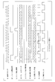
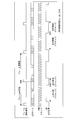
- FIG. 9 is a timing chart of various signals showing that the light emission amount of the light source changes with respect to the time per frame when the frame period of the video signal changes.
- the frame start signal consists of a frame pulse train corresponding to the frame period of the video signal.
- the first and second frame pulses correspond to a frame frequency of 60 Hz, for example, and the second and third frame pulses correspond to a frame frequency of 50 Hz, for example.
- the frame frequency is If it is changed to be smaller, the frame period becomes longer.
- the LED data is composed of a data string in which each LED is turned on / off in turn at a predetermined lighting time when a plurality of (number 0 to n) LEDs (light-emission-diodes) are used as the light source. .
- the PWM (pulse width modulation) clock gives the timing for extracting the pulse width when the LED lighting signal is pulse width modulated according to the LED data.
- the lighting time of each LED is set constant. In the example of FIG. 9, for the convenience of explanation, it is assumed that the lighting time is set to 7 clocks of the PWM clock. Since the frame period (short period) of the first and second frame pulses is detected to be 10 clocks using the PWM clock, the period of the LED lighting signal generated in synchronization with the frame pulse is also 10 clocks. On the other hand, since the frame period (long period) of the second and third frame pulses is detected to be 12 clocks using the same PWM clock, the period of the LED lighting signal is also 12 clocks. Yes.
- each LED is turned on for the above-mentioned 7 clocks, so the turn-off time for the short period is 3 clocks, and the turn-off time for the long period is 5 clocks. It turns out that it becomes. Therefore, when the frame period is long, the extinguishing time with respect to the time per frame is long, so that the light emission rate with respect to the time per frame is lowered, resulting in a dark display screen.
- the lighting brightness of the light source is defined by the following equation.
- Lighting brightness Maximum LED brightness x Lighting time / (Lighting time + Light-off time)
- the frame period is changed by providing the display device with separate lighting time / extinguishing time data for each video signal source or each display device destination.
- a method for switching the setting of the lighting time or the light-off time can be considered.
- this method has a disadvantage in terms of the cost of the display device and the response speed because the required memory increases and the control program becomes complicated.
- an unknown video signal is input to the display device, it may not be possible to cope with it.
- the present invention has been made to solve the above-described problems, and its purpose is to change the source of the video signal, change the destination of the display device, or change the destination of the unknown video signal to the display device.
- a clock generation method and a clock generation circuit for generating a clock suitable for performing lighting control in which the light emission amount of the light source does not change with respect to the time per frame even when input, and lighting control using the clock A method, a light source control circuit, and a display device are provided.
- a lighting control method uses a pulse width modulation method to turn on a light source that irradiates the display screen in synchronization with a video signal that rewrites the display screen at a constant period.
- the pulse interval of the first clock that gives the timing for generating the light source driving signal by determining the pulse width corresponding to the lighting time or the lighting time is changed in conjunction with the change of the period,
- a modulation clock is generated in which the number of clocks of the first clock for one cycle is maintained at a constant value regardless of the change of the cycle, and even if the cycle changes, the lighting time and the turn-off time within one cycle are It is characterized by keeping the ratio constant.
- the video on the display screen is rewritten at a constant cycle.
- One image can be displayed on the display screen by one cycle of the video signal, and the one image is called a frame, for example.
- the lighting and extinguishing of the light source that illuminates the display screen are controlled in synchronization with a fixed cycle of rewriting the video.
- the lighting time or extinguishing time at that time is determined by the pulse width of the light source driving signal.
- the timing for determining the pulse width is given by the first clock and the number of clocks.
- the pulse interval of the first clock that is, the time interval from the rising edge of a certain pulse of the first clock to the rising edge of the next pulse is interlocked with the change of the cycle for rewriting the display screen.
- a modulation clock is generated in which the number of clocks of the first clock with respect to one cycle of the cycle is maintained at a constant value regardless of the change of the cycle. Keep the ratio between time and turn-off time constant.
- the pulse interval of the first clock is extended in conjunction with the longer cycle, and the number of clocks of the first clock for one cycle of the cycle is changed. Do not.
- the light source drive signal is given a timing that determines the pulse width of the lighting time and the light-off time by the first clock whose cycle number is extended and whose clock number is not changed.
- the turn-on time and the turn-off time are extended in conjunction with a long cycle so as to keep the ratio between the turn-on time and the turn-off time within one cycle constant.
- the pulse interval of the first clock is shortened in conjunction with the shorter cycle. Also in this case, since the number of clocks of the first clock with respect to one cycle of the cycle does not change, the lighting time and the lighting time are short so that the ratio between the lighting time and the lighting time within one cycle is kept constant. As a result, it shrinks in conjunction with the cycle.
- the clock generation method of the present invention uses a pulse width modulation method to turn on and off the light source that illuminates the display screen in synchronization with a video signal that rewrites the display screen at a constant period.
- the clock generation method for generating the first clock for controlling in accordance with the second clock as a reference the number of clocks A obtained by detecting the period by the second clock, and 1 of the period
- the second clock is divided by A / B based on the total number of clocks B of the first clock set to a predetermined value so as to determine the total time of the lighting time and the lighting time corresponding to the period.
- a frequency-divided clock is generated as the first clock.
- the resulting clock number A is changed when the cycle is changed. It changes in conjunction with the cycle.
- the total clock number B of the first clock that determines the total time of the light source lighting time and the light extinguishing time corresponding to one cycle does not change because it is set to a constant value in advance.
- the divided clocks divided by A / B have the same number of clocks included in one period regardless of whether the number of clocks included in one period is one period before the change or one period after the change.
- the clock becomes the number B.
- a clock generation circuit generates a first clock synchronized with a periodic signal composed of a periodic pulse train based on a second clock as a reference.
- the detection circuit detects the period of the periodic signal as the clock number A of the second clock, the clock number A output from the detection circuit, and a constant value corresponding to one period of the period.
- a frequency dividing circuit that inputs the total clock number B of the first clock and outputs the divided clock obtained by dividing the second clock by A / B as the first clock.
- the number of clocks A as a result is the changed period when the period is changed. It changes in conjunction.
- the total clock number B of the first clock corresponding to one period of the period is not changed because it is set to a constant value in advance.
- the divided clocks divided by A / B have the same number of clocks included in one period regardless of whether the number of clocks included in one period is one period before the change or one period after the change.
- the clock becomes the number B. That is, even if the frequency of the periodic signal changes, the frequency-divided clock of the present invention maintains the synchronization with the periodic signal by having the same period as the periodic signal, and the number of clocks per period does not change. Become a clock.
- the periodic signal is the video signal.
- the above-mentioned frequency-divided clock can be used as a clock suitable for light source control that keeps the ratio between the lighting time and the light-off time within one cycle constant.
- the clock generation circuit of the present invention uses a pulse width modulation method to turn on and off the light source that irradiates the display screen in synchronization with a video signal that rewrites the display screen at a constant period.
- a detection circuit that detects the period of the video signal as the number of clocks A of the second clock in a clock generation circuit that generates a first clock for control in step 2 based on a second clock as a reference;
- the clock number A output from the detection circuit and the total clock number B of the first clock that determines the total time of the lighting time and the light-off time corresponding to one cycle of the cycle are input, and the second clock And a frequency dividing circuit that outputs a frequency-divided clock obtained by frequency-dividing A / B as the first clock.
- the frequency dividing circuit in the clock generation circuit of the present invention further includes a comparison / selection circuit, an output circuit, and an addition circuit for adding the output value of the comparison / selection circuit and the total clock number B, and the comparison / selection circuit.
- the circuit compares the clock number A with the output value C of the adder circuit, and outputs the output value C when the output value C is less than the clock number A.
- the output circuit C is configured to output a value obtained by subtracting the clock number A from the output value C, and the output circuit has the output value C equal to or greater than the clock number A. It is configured to output a pulse every time.
- the comparison / selection circuit outputs the output value C as it is during the period T1 in which the output value C of the adder circuit does not exceed the clock number A of the second clock, and the output value C is equal to or greater than the clock number A.
- the period T2 exceeds, the value obtained by subtracting the clock number A from the output value C is output.
- the comparison / selection circuit further compares the clock number A with the output value C of the adder circuit, and subtracts the clock number A from the output value C of the adder circuit.
- the output of the comparison circuit indicates that the output of the subtraction circuit, the output of the comparison circuit, the output of the addition circuit, and the output of the subtraction circuit are input and the output value C is less than the clock number A. If the output of the comparator circuit indicates that the output value C is equal to or greater than the clock number A, the output value C of the adder circuit is selected. And a selection circuit for outputting the output.
- a clock generation circuit that generates a divided clock obtained by dividing the second clock by A / B can be realized with a simple configuration.
- the comparison and selection circuit in the clock generation circuit of the present invention further includes a first latch circuit that latches an output of the selection circuit using the second clock and outputs the latched signal to the adder circuit. This is preferable for generating a divided clock obtained by dividing the clock by A / B.
- the output circuit is a second latch circuit that latches the output of the comparison circuit using the second clock, and the divided clock obtained by dividing the second clock by A / B is used. It is further preferable in producing.
- the clock generation circuit of the present invention is configured by a digital circuit.
- PLL Phase Lock Loop
- the divided clock can be generated within one period when the period is changed. Therefore, the change in the luminance of the display screen due to the change in the light emission amount of the light source is suppressed to the minimum, and the change in the luminance can be prevented from being recognized by the observer of the display screen.
- the detection circuit in the clock generation circuit of the present invention further includes a period limiting circuit for giving a predetermined maximum value and minimum value with respect to the period.
- the period exceeding the maximum value or the period falling below the minimum value is an abnormal period that is not assumed as a video signal input to the display device. Therefore, by providing a cycle limiting circuit in the detection circuit, various malfunctions can be prevented from occurring.
- various malfunctions include, for example, a frequency-divided clock that is generated based on an abnormal period, and the lighting time of the light source becomes inappropriately long, and as a result, the light source blinks slowly enough to be visually recognized.
- the light source drive circuit may cause an abnormal operation.
- a light source control circuit receives the clock generation circuit described above and the video signal and supplies a synchronization signal indicating the period to the clock generation circuit.
- a light source control data generation circuit that generates a lighting control signal that determines a lighting time, and the lighting control signal input from the light source control data generation circuit when the on / off control of the light source is synchronized with the synchronization signal.
- a light source driving circuit for generating a light source driving signal by counting the lighting time shown using the frequency-divided clock input from the clock generating circuit.
- the detection circuit provided in the clock generation circuit obtains the clock number A using the synchronization signal supplied from the light source control data generation circuit and the second clock. be able to.
- the clock generation circuit can generate a divided clock obtained by dividing the second clock by A / B and output the divided clock to the light source driving circuit.
- the light source control data generation circuit generates a lighting control signal that determines the lighting time of the light source, and outputs it to the light source driving circuit.
- the light source driving circuit that has obtained the divided clock and the lighting control signal counts the lighting time indicated by the lighting control signal using the divided clock, and generates a light source driving signal synchronized with the video signal. Can do.
- the light source drive signal is generated using a frequency-divided clock suitable for light source control so as to keep the ratio between the lighting time and the light-off time within one cycle constant even when the constant cycle at which the video is rewritten is changed. Therefore, even if the source of the video signal is changed, the destination of the display device is changed, or an unknown video signal is input to the display device, the change in display brightness is suppressed. be able to.
- the lighting time and the lighting time may be controlled to be constant, but the lighting time and the lighting time may be dynamically changed as necessary.
- the present invention can be applied.
- the average luminance of the video signal is obtained and the backlight lighting time and the lighting time are changed according to the average luminance.
- the display screen is divided into a plurality of areas, and the lighting time and the lighting time of the light source arranged in each area are changed according to the distribution of the luminance obtained from the video signal, (3) According to the brightness of the room For example, a mode in which the backlight lighting time and the light-off time are changed can be considered.
- the display device of the present invention is configured to determine the light source control circuit, the light source controlled to be turned on by the light source control circuit, and the amount of light emitted from the light source based on the video signal. And a display panel for modulating and displaying an image.
- the luminance of the display can be reduced.
- a display device capable of suppressing changes can be provided.
- a combination of a configuration described in a certain claim and a configuration described in another claim is limited to a combination of the configuration described in the claim cited in the claim.
- combinations with configurations described in the claims not cited in the focused claims are possible.
- the pulse interval of the first clock that gives the timing for generating the light source driving signal by determining the pulse width corresponding to the lighting time or the lighting time is changed.
- a modulation clock is generated in which the number of clocks of the first clock for one cycle of the cycle is maintained at a constant value regardless of the change of the cycle, and within one cycle even if the cycle changes.
- the light emission rate per period does not change, so the source of the video signal is changed, the destination of the display device is changed, or the unknown video Even when a signal is input to the display device, the display luminance is not changed.
- the number A of clocks obtained by detecting the period of the video signal with the second reference clock, and the lighting time and light extinction corresponding to one period of the period is used as the first clock. It is a method of generating.
- the clock generation circuit detects the period of the periodic signal as the clock number A of the second clock as a reference, the clock number A output from the detection circuit, The total clock number B of the first clock set to a constant value corresponding to one period of the cycle is input, and the divided clock obtained by dividing the second clock by A / B is used as the first clock. And a frequency dividing circuit for output.
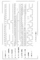
- FIG. 4 is a timing chart showing an example of timings of various signals related to generation of a PWM clock in the clock generation circuit shown in FIG. 3.
- FIG. 4 is a timing chart showing other timing examples of various signals related to generation of a PWM clock in the clock generation circuit shown in FIG. 3.
- FIG. 4 is a timing chart showing still another timing example of various signals related to generation of a PWM clock in the clock generation circuit shown in FIG. 3.
- FIG. 1 It is a timing chart which shows the light source drive signal which controls ON / OFF of the several light source shown in FIG. It is a block diagram which shows the other structural example of the clock generation circuit of this invention. It is a timing chart which shows the timing of the various signals used for the lighting control method with the subject which this invention should solve.
- FIGS. 1 to 7 An embodiment of the present invention will be described with reference to FIGS. 1 to 7 as follows.
- each drawing referred to below is a simplified illustration of only a main part necessary for explaining the present invention, out of the configuration of one embodiment of the present invention, for convenience of explanation. Any configuration not shown in each of the referenced drawings can be included.
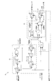
- FIG. 1 shows a configuration of a display device 1 which is an embodiment of the display device of the present invention.
- the display device 1 includes a light source control circuit 2, a backlight 3 that is controlled to be turned on by the light source control circuit 2, and a liquid crystal that modulates the amount of light emitted from the backlight 3 based on a video signal and displays an image.
- a panel 4 display panel
- the backlight 3 includes a plurality of light sources 30 on the back side of the liquid crystal panel 4 and can irradiate the entire display screen with uniform light from the back side of the display screen. Yes. However, if the size of the display screen is small like a mobile phone, the light source 30 is arranged at one end on the back side of the display screen and replaced with a sidelight type having a configuration for guiding uniform light over the entire display screen. Can do.
- the plurality of light sources 30 are, for example, n + 1 LED groups (LED0 to LEDn) as shown in FIG.
- the light source 30 is not limited to the LED as long as it can control blinking in synchronization with the video signal.
- the light source control circuit 2 includes a PLL (phase-locked loop) 6 described later in detail as a clock generation circuit of the present invention, a backlight data calculation circuit 7 (light source control data generation circuit), and an LED driver. 8 (light source driving circuit).
- PLL phase-locked loop
- backlight data calculation circuit 7 light source control data generation circuit
- LED driver. 8 light source driving circuit
- the backlight data calculation circuit 7 is supplied with the video signal, supplies a frame start signal (synchronization signal) indicating the frame period of the video signal to the PLL 6, and LED data (lighting up) that determines the lighting time of the light source 30. Control signal). Further, when the LED driver 8 controls on / off of the light source 30 so as to be synchronized with the synchronization signal, the LED driver 8 inputs the lighting time indicated by the LED data input from the backlight data calculation circuit 7 from the PLL 6.
- the light source drive signal is generated by counting using the PWM clock (first clock, frequency-divided clock or modulation clock).
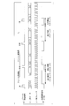
- FIG. 2A shows a frame start signal that gives the start timing of the frame period for each period.
- FIG. 2D shows a light source drive signal given from the LED driver 8 to the LED 0 that starts to be turned on / off first among the LED groups (LED0 to LEDn).
- the light source drive signal is output from the LED driver 8 in synchronization with the PWM clock that rises after the frame start signal falls, as shown in FIGS. 2 (a), 2 (c), and 2 (d).
- the pulse width of the light source drive signal is determined by the LED data generated by the backlight data calculation circuit 7.
- the LED data is output from the backlight data calculation circuit 7 to the LED driver 8 in order corresponding to each of the LED groups (LED0 to LEDn) as shown in FIG.
- the lighting time of LED0 is set to 7 PWM clocks by LED data for convenience of explanation.
- the turn-off time of LED0 is 3 PWM clocks. Therefore, the ratio between the lighting time and the lighting time within one frame period is 7/3.
- FIG. 7 shows light source driving signals sequentially given from the LED driver 8 to the LEDs 0 to LEDn.
- FIG. 7 shows an example in which the frame period is constant (10 clocks) and the lighting time of each LED is also set to the same (7 clocks).
- the turning on and off of the light source 30 that irradiates the display screen is controlled in synchronization with a certain cycle in which the video is rewritten.
- the lighting time or extinguishing time at that time is determined by the pulse width of the light source driving signal, and the timing for determining the pulse width is given by the PWM clock and the number of clocks.
- the pulse interval of the PWM clock that is, the time interval from the rising edge of one pulse of the PWM clock to the rising edge of the next pulse is linked to the change of the frame period.
- a modulation clock is generated in which the number of PWM clocks for one frame period is maintained at a constant value regardless of the change of the frame period. Even if the frame period changes, the lighting time and the light extinction within one frame period are changed. The ratio with time is kept constant.
- the pulse interval of the PWM clock shown in (c) of FIG. 2 is the frequency without changing the number of clocks included in one frame period from the next period t 1 (see (a) of FIG. 2) after the frame period is changed. It turns out that it was changed so that it may become small.
- the pulse interval of the PWM clock is extended in conjunction with the longer cycle. Since the number of clocks per frame period of the PWM clock that gives the timing for determining the pulse width of the light source drive signal does not change, the lighting time is, for example, 7 clocks, and the light-off time is maintained for 3 clocks. That is, the PWM clock is extended in association with a long cycle so as to keep the ratio between the lighting time and the lighting time within one frame cycle constant.
- the pulse interval of the PWM clock may be shortened in conjunction with the shorter cycle.
- the number of clocks per frame period of the PWM clock that gives the timing for determining the pulse width of the light source drive signal does not change, so the lighting time and the lighting time are the lighting time and the lighting time within one frame period.
- the ratio is contracted in association with a short cycle so as to keep the ratio of.
- the lighting control method of the present invention even if the fixed cycle in which the video is rewritten is changed, the light emission rate per cycle does not change. Even when the destination is changed or an unknown video signal is input to the display device, the display brightness does not change.
- the PLL 6 (clock generation circuit) for generating a PWM clock suitable for implementing the lighting control method of the present invention described above will be described below.
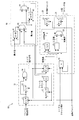
- the PLL 6 generates the PWM clock based on a reference clock (second clock) having a higher frequency than the PWM clock. Therefore, the main part of the PLL 6 includes a detection circuit 10 and a frequency dividing circuit 20 as shown in FIG.
- the detection circuit 10 detects the frame period (period of the periodic signal) of the video signal as the clock number A of the reference clock.
- the frequency dividing circuit 20 is configured such that the number of clocks A output from the detection circuit 10 and the total number of clocks B of the PWM clock that determines the total time of turn-on time and turn-off time per one cycle of the frame period (the period The total number of clocks B) set to a constant value corresponding to one cycle of the above is input, and the PWM clock is generated and output as a divided clock obtained by dividing the reference clock by A / B.
- the present invention is not limited to whether the total clock number B is fixed or variable.
- the total clock number B is described as being generated by the backlight data calculation circuit 7 and supplied to the frequency divider circuit 20 of the PLL 6 for convenience. Since the detailed configuration and detailed operation of the detection circuit 10 and the frequency dividing circuit 20 will be described later, the outline of the operation will be described here.
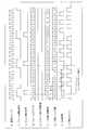
- FIG. 4 shows a timing chart of various signals related to the PLL 6.
- the detection circuit 10 is included in the frame period using the frame start signal (FIG. 4B) and the reference clock (FIG. 4A) supplied from the backlight data calculation circuit 7.
- the number of reference clocks to be detected is detected.
- This clock number is the above-mentioned clock number A as a period value, and in the example of FIG. 4, it is obtained as a period value 7 in FIG.
- the detection circuit 10 since the detection circuit 10 detects the frame period of the video signal using the reference clock, the number of clocks A (period value 7) as a result is obtained when the frame period is changed. Furthermore, it changes in conjunction with the changed frame period.
- the total clock number B that determines the lighting time and the light-off time per frame period of the light source 30 is fixed and does not change. For example, in FIG. 4I, the total clock number B is set to 3 for convenience of explanation.
- the frequency-divided clock divided by A / B has the same number of clocks included in one frame period as for one frame period before the change and one frame period after the change.
- the clocks have the same total clock number B. This is because, for example, if the fixed cycle for rewriting the display screen is changed to a long cycle, the total number of clocks B included in one cycle does not change. This means that a peripheral clock is generated. On the other hand, even if the fixed cycle for rewriting the display screen is changed to a short cycle, the total clock number B included in one cycle does not change. Is generated.
- the detection circuit 10 includes latch circuits 11, 12, and 13, an AND circuit 14 in which one of the two inputs is an inverting input, a counter 15, and an increment circuit 16. .
- the latch circuit 11 latches the frame start signal supplied from the backlight data calculation circuit 7 using a reference clock.
- the latch circuit 12 latches the output of the latch circuit 11 using the reference clock.
- the output of the latch circuit 11 is further input to the AND circuit 14 as it is, while the output of the latch circuit 12 is inverted and input to the AND circuit 14.
- the output of the AND circuit 14 is input to the counter 15 and also to the latch circuit 13 as an edge detection signal for detecting each edge of the pulse train of the frame start signal.
- the edge detection signal input to the latch circuit 13 gives the output timing of the latch circuit 13.
- the output of the counter 15 is latched by the latch circuit 13 via the increment circuit 16. Note that the counter 15 counts the length of the frame period as the number of clocks of the reference clock, so it can also be called a frame counter.
- an edge detection signal that becomes high level by one reference clock is output from the AND circuit 14 in synchronization with the frame start signal.
- the counter 15 outputs a count value every time a reference clock is input, but resets the count value to 0 when an edge detection signal is input.
- the increment circuit 16 causes the latch circuit 13 to latch a value obtained by adding +1 to the count value every time the reference clock is input.
- the latch circuit 13 outputs the value latched when the edge detection signal becomes high level. As shown in FIG. 4D, when the edge detection signal becomes high level, the counter 15 outputs 6 as a value before resetting, so the latch circuit 13 latches 7.
- the detection circuit 10 detects the frame period of the video signal based on the number of clocks of the reference clock, and when the edge detection signal becomes a high level, the period value 7 as the clock number A is obtained from the latch circuit 13. Output.
- the frequency dividing circuit 20 adds a comparison / selection circuit 21, a latch circuit 22 (second latch circuit) as an output circuit, and an output value of the comparison / selection circuit 21 and the total clock number B. Circuit 23.
- the comparison / selection circuit 21 compares the clock number A with the output value C of the adder circuit 23, and outputs the output value C when the output value C is less than the clock number A. When the value C becomes equal to or greater than the clock number A, a value obtained by subtracting the clock number A from the output value C is output.
- the comparison / selection circuit 21 compares the clock number A with the output value C of the adder circuit 23, and subtracts the clock number A from the output value C of the adder circuit 23.
- the subtraction circuit 25, the output of the comparison circuit 24, the output of the addition circuit 23, and the output of the subtraction circuit 25 are input, and the comparison is made that the output value C is less than the clock number A.
- the output of the circuit 24 indicates that the output value C of the adder circuit 23 is selected
- the output of the comparison circuit 24 indicates that the output value C is equal to or greater than the clock number A
- a selection circuit 26 for selecting and outputting the output of the subtraction circuit 25.
- the output of the selection circuit 26 is fed back to the addition circuit 23 via a latch circuit 27 (first latch circuit).
- the latch circuit 22 is configured to output a pulse each time the output value C becomes equal to or greater than the clock number A. Eventually, the output of the latch circuit 22 becomes the PWM clock obtained by dividing the reference clock by A / B.
- the comparison circuit 24 compares the clock number A input from the detection circuit 10 with the output value C of the addition circuit 23, and the comparison result is sent to the latch circuit 22 and the selection circuit 26. Output.
- the comparison circuit 24 outputs 0 as the comparison result to the latch circuit 22 and the selection circuit 26 as shown in FIG. .
- the selection circuit 26 In response to the comparison result, the selection circuit 26 outputs the output value C (for example, in the period T1 (see (f) of FIG. 4)) in which the output value C of the addition circuit 23 does not exceed the clock number A of the second clock. 3 or 6) is output as it is, and the value obtained by subtracting the clock number A from the output value C is output in the subtracting circuit 25 in the period T2 when the output value C exceeds the clock number A or more. For example, when the output value C is 9, the selection circuit 26 outputs 2, which is a difference from 7 of the clock number A.
- the output of the selection circuit 26 is latched by the latch circuit 27, is output from the latch circuit 27 as the output of the comparison selection circuit 21 with a delay of one clock, and is fed back to the adder circuit 23.
- the adder circuit 23 adds the fed back output value (frequency dividing counter value) of the comparison / selection circuit 21 and the total clock number B.
- the comparison / selection circuit 21 outputs a high-level signal as a comparison result, as shown in FIG.
- the latch circuit 22 latches the comparison result and outputs it as a PWM clock with a delay of one clock as shown in FIG.
- the frequency dividing counter value and the output value C circulate in the same cycle as the frame cycle.
- the reference clock having the clock number A per frame period has the total clock number B per frame period, that is, A / B division. Converted to a divided clock.
- the comparison / selection circuit 21 A high level signal is output as a comparison result.
- the latch circuit 22 latches the comparison result and outputs it as a PWM clock with a delay of one clock, as shown in FIG.
- the output value C and the frequency division counter value shown in (f) and (g) of FIG. 5 circulate at the same cycle as the frame cycle, as in (f) and (g) of FIG.
- the reference clock having the clock number A per frame period has the total clock number B per frame period, that is, divided by A / B. It has been converted to a divided clock.
- the clock number A of the reference clock obtained by detecting the frame period and the constant total clock number B set per frame can be converted into a PWM clock obtained by dividing the A / B frequency regardless of the length of the frame period.
- the total number of clocks B per frame period of the PWM clock synchronized with the changed frame period can be kept constant. Therefore, as described with reference to FIG. 2, the video signal source is changed, the destination of the display device is changed, or an unknown video signal is input to the display device.
- the ratio of the lighting time and the lighting time of the light source driving signal controlled by the number of PWM clocks can be kept constant, the lighting brightness of the light source 30 can always be kept constant.
- the number of clocks per frame period of the PWM clock does not become the total number B of clocks, but fluctuates.
- the number of clocks per frame period of the PWM clock is held at the total clock number B as described with reference to FIGS.
- the main cause of the fluctuation is the period value (clock number A) obtained by detecting the frame period, as shown in FIG. 6 (e), the period value obtained before the frame period is changed. It must be used.
- the light source 30 can be accurately controlled within one frame period after the frame period is changed.
- the effect of this high speed operation is because the clock generation circuit of the present invention is constituted by a digital circuit.
- FIG. 8 shows another configuration example of the clock generation circuit of the present invention.
- the clock generation circuit 6A shown in FIG. 8 defines a maximum value and a minimum value of the clock number A (period value) in the clock generation circuit 6 shown in FIG. This is different from the clock generation circuit 6 in that a period limiting circuit 40 is added.
- the value of the counter 15 becomes very large, and an unexpectedly large clock number A may be output to the frequency dividing circuit 20.
- the cycle of the PWM clock is abnormally extended, the light source 30 is turned on for a long time, or the on / off control cycle of the light source 30 is extended. .
- the clock generation circuit of the present embodiment can suppress the occurrence of such a problem and improve the reliability.
- the period limiting circuit 40 includes comparison circuits 41 and 43 and selection circuits 42 and 44.
- the comparison circuit 41 receives the predetermined maximum value M and the output value D of the increment circuit 16 and determines whether or not the output value D exceeds the maximum value M (D> M). If D> M is not satisfied, the comparison circuit 41 outputs 0 as the determination result to the selection circuit 42. If D> M, the comparison circuit 41 outputs 1 as the determination result to the selection circuit 42.
- the selection circuit 42 receives the maximum value M and the output value D, and outputs either the maximum value M or the output value D according to the determination result of the comparison circuit 41. That is, when the determination result 0 of the comparison circuit 41 is input to the selection circuit 42, the selection circuit 42 outputs the output value D to the comparison circuit 43 and the selection circuit 44, while the determination result 1 of the comparison circuit 41 is selected. When input to the circuit 42, the selection circuit 42 outputs the maximum value M to the comparison circuit 43 and the selection circuit 44.
- a predetermined minimum value m and an output value E (one of M or D) of the selection circuit 42 are input to the comparison circuit 43, and the output value E is smaller than the minimum value m (m> E ) Is determined. If not m> E, the comparison circuit 43 outputs 0 as the determination result to the selection circuit 44. If m> E, the comparison circuit 43 outputs 1 to the selection circuit 44 as the determination result.
- the selection circuit 44 receives the minimum value m and the output value E, and outputs either the minimum value m or the output value E according to the determination result of the comparison circuit 43. That is, when the determination result 0 of the comparison circuit 43 is input to the selection circuit 44, the selection circuit 44 outputs the output value E to the latch circuit 13 of the detection circuit 10, while the determination result 1 of the comparison circuit 43 is the selection circuit. When input to 44, the selection circuit 44 outputs the minimum value m to the latch circuit 13.
- the selection circuit 44 when D> M and the maximum value M is output when D> M, the selection circuit 44 always outputs the maximum value M to the latch circuit 13 because D ⁇ M.
- the present invention can be applied to a clock generation circuit that generates a first clock synchronized with a periodic signal such as a video signal based on a second clock as a reference, and further, in synchronization with the periodic signal,
- the present invention can be applied to a light source control circuit that controls on / off of a light source and a display device including such a light source control circuit.
- SYMBOLS 1 Display apparatus 2 Light source control circuit 4 Liquid crystal panel (display panel) 6 PLL (Clock Generation Circuit) 7 Backlight data calculation circuit (light source control data generation circuit) 8 LED driver (light source drive circuit) DESCRIPTION OF SYMBOLS 10 Detection circuit 20 Frequency dividing circuit 21 Comparison selection circuit 22 Latch circuit (2nd latch circuit) 23 addition circuit 24 comparison circuit 25 subtraction circuit 26 selection circuit 27 latch circuit (first latch circuit) 30 light source 40 period limiting circuit
Landscapes
- Engineering & Computer Science (AREA)
- Multimedia (AREA)
- Signal Processing (AREA)
- Physics & Mathematics (AREA)
- Computer Hardware Design (AREA)
- General Physics & Mathematics (AREA)
- Theoretical Computer Science (AREA)
- Liquid Crystal Display Device Control (AREA)
- Control Of Indicators Other Than Cathode Ray Tubes (AREA)
- Liquid Crystal (AREA)
Abstract
Description
まず、上述のように映像信号のソースが変更される場合には、例えば、映像信号としてのテレビ放送信号を、DVD(digital versatile disk)プレーヤのような他のビデオソースから供給される映像信号に切り換える場合が該当する。例えば、我が国で視聴されているテレビ放送信号は、NTSC方式に準拠しており、フレーム周波数は60Hzに定められている。一方、他のビデオソースから供給される映像信号には、映画館で上映される映画を基に作成した映像信号のように、フレーム周波数が24Hzに定められているものがある。
点灯輝度=LEDの最大輝度×点灯時間/(点灯時間+消灯時間)
このように、映像信号のフレーム周期に同期して光源を制御するにあたって、決まったPWMクロックで光源を点灯させようとすると、フレーム周期が変更された場合に、点灯輝度が変わる。その理由は要するに、フレーム周期と同期を取るために、消灯時間を延ばしたり、あるいは点灯時間を延ばしたりする結果になるからである。上記の式から、消灯時間を延ばした場合には点灯輝度が低下し、点灯時間を延ばした場合には点灯輝度が上昇することになる。
本発明の実施の一形態について図1ないし図7に基づいて説明すれば、以下のとおりである。なお、以下で参照する各図は、説明の便宜上、本発明の一実施形態の構成のうち、本発明を説明するために必要な主要部のみを簡略化して示したものなので、本明細書が参照する各図に示されていない任意の構成を含むことができる。
図1に、本発明の表示装置の一実施形態である表示装置1の構成を示す。表示装置1は、光源制御回路2と、光源制御回路2によって点灯を制御されるバックライト3と、バックライト3が出射する光の光量を、映像信号に基づいて変調し、映像を表示する液晶パネル4(表示パネル)とを備えている。
上述した本発明の点灯制御方法を実施するのに適したPWMクロックを生成する上記PLL6(クロック生成回路)について、以下説明する。
上記検出回路10の詳細な構成と動作をさらに説明する。図3に示すように、検出回路10は、ラッチ回路11,12,13と、2つの入力の一方が反転入力となっているAND回路14と、カウンタ15と、インクリメント回路16とを備えている。
続いて、上記分周回路20は、比較選択回路21と、出力回路としてのラッチ回路22(第2ラッチ回路)と、上記比較選択回路21の出力値と上記トータルクロック数Bとを加算する加算回路23とを備えている。
上記の構成によれば、まず、比較回路24が、検出回路10から入力されたクロック数Aと、加算回路23の出力値Cとを比較し、比較結果をラッチ回路22および選択回路26に対して出力する。
次に、フレーム周期が、図4の例に比べて長く変化した場合について、図5に基づいて説明する。
次に、フレーム周期が変化した直後の分周回路20の動作について、図6に基づいて説明する。
本発明の他の実施の形態について図8に基づいて説明すれば、以下のとおりである。なお、説明の便宜上、前記の実施の形態1の図面に示した部材と同一の機能を有する部材については、同一の符号を付し、その説明を省略する。
以下、周期制限回路40の構成と動作とを説明する。周期制限回路40は、比較回路41,43と、選択回路42,44とを備えている。
2 光源制御回路
4 液晶パネル(表示パネル)
6 PLL(クロック生成回路)
7 バックライトデータ計算回路(光源制御データ生成回路)
8 LEDドライバ(光源駆動回路)
10 検出回路
20 分周回路
21 比較選択回路
22 ラッチ回路(第2ラッチ回路)
23 加算回路
24 比較回路
25 減算回路
26 選択回路
27 ラッチ回路(第1ラッチ回路)
30 光源
40 周期制限回路
Claims (12)
- 表示画面を一定の周期で書き換える映像信号に同期して、上記表示画面を照射する光源の点灯時間をパルス幅変調方式にて制御する点灯制御方法において、
上記点灯時間または消灯時間に対応したパルス幅を決めて光源駆動信号を生成するタイミングを与える第1クロックのパルス間隔を、上記周期の変更に連動して変更し、上記周期の1周期に対する上記第1クロックのクロック数を、上記周期の変更によらず一定値に維持した変調クロックを生成し、上記周期が変わっても、1周期内の点灯時間と消灯時間との比率を一定に保つこと
を特徴とする点灯制御方法。 - 表示画面を一定の周期で書き換える映像信号に同期して、上記表示画面を照射する光源の点灯時間および消灯時間をパルス幅変調方式にて制御するための第1クロックを、基準となる第2クロックを元にして生成するクロック生成方法において、
上記第2クロックによって上記周期を検出して得たクロック数Aと、上記周期の1周期分に対応した上記点灯時間と消灯時間の合計時間を決めるように、予め一定値に定めた上記第1クロックのトータルクロック数Bとに基づいて、上記第2クロックをA/B分周した分周クロックを、上記第1クロックとして生成すること
を特徴とするクロック生成方法。 - 周期性の有るパルス列からなる周期性信号に同期した第1クロックを、基準となる第2クロックを元にして生成するクロック生成回路において、
上記周期性信号の周期を上記第2クロックのクロック数Aとして検出する検出回路と、
上記検出回路が出力する上記クロック数Aと、上記周期の1周期分に対応して一定値に定められた上記第1クロックのトータルクロック数Bとを入力して、上記第2クロックをA/B分周した分周クロックを、上記第1クロックとして出力する分周回路とを備えていること
を特徴とするクロック生成回路。 - 表示画面を一定の周期で書き換える映像信号に同期して、上記表示画面を照射する光源の点灯時間および消灯時間をパルス幅変調方式にて制御するための第1クロックを、基準となる第2クロックを元にして生成するクロック生成回路において、
上記映像信号の周期を上記第2クロックのクロック数Aとして検出する検出回路と、
上記検出回路が出力する上記クロック数Aと、上記周期の1周期分に対応した上記点灯時間と消灯時間の合計時間を決める上記第1クロックのトータルクロック数Bとを入力して、上記第2クロックをA/B分周した分周クロックを、上記第1クロックとして出力する分周回路とを備えていること
を特徴とするクロック生成回路。 - 上記分周回路は、さらに、
比較選択回路と、
出力回路と、
上記比較選択回路の出力値と上記トータルクロック数Bとを加算する加算回路とを備え、
上記比較選択回路は、上記クロック数Aと上記加算回路の出力値Cとを比較し、該出力値Cが上記クロック数A未満の値であるときには該出力値Cを出力し、該出力値Cが上記クロック数A以上の値になったときには、該出力値Cから上記クロック数Aを引き算した値を出力するように構成され、
上記出力回路は、上記出力値Cが上記クロック数A以上の値になる毎に、パルスを出力するように構成されていること
を特徴とする請求項3または4に記載のクロック生成回路。 - 上記比較選択回路は、さらに、
上記クロック数Aと上記加算回路の出力値Cとを比較する比較回路と、
上記加算回路の出力値Cから上記クロック数Aを引き算する減算回路と、
上記比較回路の出力と、上記加算回路の出力と、上記減算回路の出力とが入力され、上記出力値Cが上記クロック数A未満であることを、上記比較回路の出力が示している場合、上記加算回路の出力値Cを選択する一方、上記出力値Cが上記クロック数A以上であることを、上記比較回路の出力が示している場合、上記減算回路の出力を選択して出力する選択回路とを備えていること
を特徴とする請求項5に記載のクロック生成回路。 - 上記比較選択回路は、さらに、
上記選択回路の出力を上記第2クロックを用いてラッチし、上記加算回路に出力する第1ラッチ回路を備えていること
を特徴とする請求項6に記載のクロック生成回路。 - 上記出力回路は、上記比較回路の出力を上記第2クロックを用いてラッチする第2ラッチ回路であること
を特徴とする請求項6または7に記載のクロック生成回路。 - 上記クロック生成回路は、デジタル回路によって構成されていること
を特徴とする請求項3から8のいずれか1項に記載のクロック生成回路。 - 上記検出回路は、さらに、
上記周期に関して、予め定めた最大値および最小値を与える周期制限回路を備えていること
を特徴とする請求項3から9のいずれか1項に記載のクロック生成回路。 - 請求項4から10のいずれか1項に記載のクロック生成回路と、
上記映像信号が入力され、上記周期を表す同期信号を上記クロック生成回路に供給するとともに、上記光源の点灯時間を定める点灯制御信号を生成する光源制御データ生成回路と、
上記同期信号に同期するように上記光源のオンオフを制御する際に、上記光源制御データ生成回路から入力された上記点灯制御信号が示す上記点灯時間を、上記クロック生成回路から入力された上記分周クロックを用いてカウントし、光源駆動信号を生成する光源駆動回路とを備えたこと
を特徴とする光源制御回路。 - 請求項11に記載の光源制御回路と、
上記光源制御回路によって点灯を制御される光源と、
上記光源が出射する光の光量を上記映像信号に基づいて変調し、映像を表示する表示パネルとを備えたこと
を特徴とする表示装置。
Priority Applications (5)
| Application Number | Priority Date | Filing Date | Title |
|---|---|---|---|
| RU2011104239/08A RU2011104239A (ru) | 2008-10-14 | 2009-07-23 | Способ управления включением и выключением лампы, способ генерации тактового сигнала, управляющая схема источника света и дисплейное устройство |
| EP09820479A EP2337011A4 (en) | 2008-10-14 | 2009-07-23 | METHOD FOR CONTROLLING LAMP IGNITION / EXTINGUISHMENT OPERATION, CLOCK GENERATING METHOD, CLOCK GENERATING CIRCUIT, LIGHT SOURCE CONTROL CIRCUIT, AND DISPLAY DEVICE |
| JP2010533852A JPWO2010044301A1 (ja) | 2008-10-14 | 2009-07-23 | 点灯制御方法、クロック生成方法、クロック生成回路、光源制御回路および表示装置 |
| CN2009801310248A CN102119407A (zh) | 2008-10-14 | 2009-07-23 | 点亮控制方法、时钟生成方法、时钟生成电路、光源控制电路和显示装置 |
| US12/737,624 US8441429B2 (en) | 2008-10-14 | 2009-07-23 | Clock generation circuit, light source control circuit, and display device |
Applications Claiming Priority (2)
| Application Number | Priority Date | Filing Date | Title |
|---|---|---|---|
| JP2008265620 | 2008-10-14 | ||
| JP2008-265620 | 2008-10-14 |
Publications (1)
| Publication Number | Publication Date |
|---|---|
| WO2010044301A1 true WO2010044301A1 (ja) | 2010-04-22 |
Family
ID=42106468
Family Applications (1)
| Application Number | Title | Priority Date | Filing Date |
|---|---|---|---|
| PCT/JP2009/063150 Ceased WO2010044301A1 (ja) | 2008-10-14 | 2009-07-23 | 点灯制御方法、クロック生成方法、クロック生成回路、光源制御回路および表示装置 |
Country Status (6)
| Country | Link |
|---|---|
| US (1) | US8441429B2 (ja) |
| EP (1) | EP2337011A4 (ja) |
| JP (1) | JPWO2010044301A1 (ja) |
| CN (1) | CN102119407A (ja) |
| RU (1) | RU2011104239A (ja) |
| WO (1) | WO2010044301A1 (ja) |
Cited By (7)
| Publication number | Priority date | Publication date | Assignee | Title |
|---|---|---|---|---|
| JP2011112882A (ja) * | 2009-11-27 | 2011-06-09 | Renesas Electronics Corp | Led制御装置およびled制御方法 |
| JP2013088526A (ja) * | 2011-10-14 | 2013-05-13 | Sharp Corp | 信号生成回路、バックライト点灯タイミング制御回路、信号生成方法 |
| JP2013156298A (ja) * | 2012-01-26 | 2013-08-15 | Sharp Corp | 画像表示装置 |
| JP2013205574A (ja) * | 2012-03-28 | 2013-10-07 | Canon Inc | バックライト装置、バックライト装置の制御方法、及び、液晶表示装置 |
| JP2019004412A (ja) * | 2017-06-19 | 2019-01-10 | パナソニックIpマネジメント株式会社 | 光源変調回路及び方法、並びにプロジェクタ装置 |
| CN112967670A (zh) * | 2021-03-03 | 2021-06-15 | 北京集创北方科技股份有限公司 | 显示驱动方法、装置和芯片、显示设备以及存储介质 |
| JP2024506423A (ja) * | 2021-12-14 | 2024-02-14 | ティーシーエル チャイナスター オプトエレクトロニクス テクノロジー カンパニー リミテッド | 表示パネル及びその駆動方法 |
Families Citing this family (12)
| Publication number | Priority date | Publication date | Assignee | Title |
|---|---|---|---|---|
| JP5336019B1 (ja) * | 2012-05-15 | 2013-11-06 | シャープ株式会社 | 表示装置、表示装置の制御方法、テレビジョン受像機、制御プログラム、および記録媒体 |
| CN102930835B (zh) * | 2012-11-16 | 2015-02-04 | 深圳市华星光电技术有限公司 | 背光调光电路及背光调光方法 |
| CN111210785B (zh) * | 2018-11-22 | 2022-09-13 | 拉碧斯半导体株式会社 | 显示装置以及数据驱动器 |
| JP6845275B2 (ja) | 2018-11-22 | 2021-03-17 | ラピスセミコンダクタ株式会社 | 表示装置及びデータドライバ |
| CN110223621B (zh) * | 2019-06-10 | 2021-12-21 | 惠科股份有限公司 | 信号调制方法、装置及显示装置 |
| JP6744456B1 (ja) * | 2019-07-11 | 2020-08-19 | ラピスセミコンダクタ株式会社 | データドライバ及び表示装置 |
| US10966296B1 (en) * | 2019-09-18 | 2021-03-30 | Novatek Microelectronics Corp | LED controller, LED control device and LED control method |
| CN112863419B (zh) * | 2021-01-27 | 2022-12-23 | 重庆惠科金渝光电科技有限公司 | 显示设备驱动方法、显示设备以及计算机可读存储介质 |
| CN114420043B (zh) * | 2022-01-27 | 2022-11-18 | 成都利普芯微电子有限公司 | 一种驱动电路、驱动芯片和显示装置 |
| CN114554647B (zh) * | 2022-03-16 | 2023-07-25 | 无锡英迪芯微电子科技股份有限公司 | 适用于矩阵式led大灯驱动的pwm产生方法及电路 |
| CN115103483A (zh) * | 2022-05-31 | 2022-09-23 | 厦门善为光电科技有限公司 | 具有开启时间设定功能的照明装置及其方法 |
| CN121773461A (zh) * | 2023-09-19 | 2026-03-31 | 雅世电子科技有限公司 | 驱动装置和显示装置 |
Citations (9)
| Publication number | Priority date | Publication date | Assignee | Title |
|---|---|---|---|---|
| JPS5479150U (ja) * | 1977-11-15 | 1979-06-05 | ||
| JPH02249306A (ja) * | 1989-03-22 | 1990-10-05 | Yokogawa Electric Corp | 再発信パルス発生装置 |
| JPH08340498A (ja) | 1995-06-13 | 1996-12-24 | Nec Robotics Eng Ltd | 輝度制御装置 |
| JP2000292767A (ja) * | 1999-04-09 | 2000-10-20 | Matsushita Electric Ind Co Ltd | 液晶表示装置 |
| JP2005274883A (ja) * | 2004-03-24 | 2005-10-06 | Sanyo Electric Co Ltd | 投射型映像表示装置 |
| JP2007241286A (ja) | 2006-03-10 | 2007-09-20 | Samsung Electronics Co Ltd | ディスプレイバックライティングの同期動作のための方法と回路 |
| JP2008096696A (ja) * | 2006-10-12 | 2008-04-24 | Sony Corp | バックライト制御装置、バックライト制御方法、および液晶表示装置 |
| JP2008139480A (ja) * | 2006-11-30 | 2008-06-19 | Toshiba Corp | バックライト制御装置、表示装置及び表示装置のバックライト制御方法 |
| JP2008145916A (ja) * | 2006-12-13 | 2008-06-26 | Nec Electronics Corp | 表示装置及び、コントローラドライバ |
Family Cites Families (17)
| Publication number | Priority date | Publication date | Assignee | Title |
|---|---|---|---|---|
| JP3027298B2 (ja) * | 1994-05-31 | 2000-03-27 | シャープ株式会社 | バックライト制御機能付き液晶表示装置 |
| US5796392A (en) * | 1997-02-24 | 1998-08-18 | Paradise Electronics, Inc. | Method and apparatus for clock recovery in a digital display unit |
| JP4036950B2 (ja) * | 1998-02-09 | 2008-01-23 | 沖電気工業株式会社 | クロック生成回路 |
| US6297816B1 (en) * | 1998-05-22 | 2001-10-02 | Hitachi, Ltd. | Video signal display system |
| JP2000241796A (ja) * | 1998-12-24 | 2000-09-08 | Sharp Corp | 液晶表示装置及び液晶表示装置の制御信号を出力する電子機器 |
| WO2003083820A1 (en) * | 2002-03-28 | 2003-10-09 | Matsushita Electric Industrial Co., Ltd. | Liquid crystal display |
| JP3869447B2 (ja) * | 2003-03-06 | 2007-01-17 | 富士通株式会社 | ディジタルpll回路 |
| KR100673689B1 (ko) * | 2003-03-20 | 2007-01-23 | 엘지전자 주식회사 | 휴대용 컴퓨터에서의 인버터 펄스 폭 변조 주파수조절장치 및 방법 |
| EP1592245A1 (en) * | 2004-04-27 | 2005-11-02 | Matsushita Electric Industrial Co., Ltd. | Adaptive generation of synchronization signals |
| JP4912597B2 (ja) * | 2004-07-13 | 2012-04-11 | パナソニック株式会社 | 液晶表示装置 |
| US7472305B1 (en) * | 2004-12-21 | 2008-12-30 | National Semiconductor Corporation | Method and apparatus for limiting the output frequency of an on-chip clock generator |
| TWI326067B (en) * | 2005-06-29 | 2010-06-11 | Mstar Semiconductor Inc | Flat display device, controller, and method for displaying images |
| KR101384283B1 (ko) * | 2006-11-20 | 2014-04-11 | 삼성디스플레이 주식회사 | 액정 표시 장치 및 그 구동 방법 |
| KR20090059179A (ko) * | 2007-12-06 | 2009-06-11 | 삼성전자주식회사 | 백라이트 장치와 이의 제어방법과 이를 갖는 액정표시장치 |
| KR101418015B1 (ko) * | 2008-02-20 | 2014-07-09 | 삼성전자주식회사 | 스큐 조정 회로 및 방법 |
| US8547321B2 (en) * | 2008-07-23 | 2013-10-01 | Apple Inc. | LED backlight driver synchronization and power reduction |
| US8373643B2 (en) * | 2008-10-03 | 2013-02-12 | Freescale Semiconductor, Inc. | Frequency synthesis and synchronization for LED drivers |
-
2009
- 2009-07-23 RU RU2011104239/08A patent/RU2011104239A/ru unknown
- 2009-07-23 EP EP09820479A patent/EP2337011A4/en not_active Withdrawn
- 2009-07-23 JP JP2010533852A patent/JPWO2010044301A1/ja active Pending
- 2009-07-23 WO PCT/JP2009/063150 patent/WO2010044301A1/ja not_active Ceased
- 2009-07-23 US US12/737,624 patent/US8441429B2/en not_active Expired - Fee Related
- 2009-07-23 CN CN2009801310248A patent/CN102119407A/zh active Pending
Patent Citations (9)
| Publication number | Priority date | Publication date | Assignee | Title |
|---|---|---|---|---|
| JPS5479150U (ja) * | 1977-11-15 | 1979-06-05 | ||
| JPH02249306A (ja) * | 1989-03-22 | 1990-10-05 | Yokogawa Electric Corp | 再発信パルス発生装置 |
| JPH08340498A (ja) | 1995-06-13 | 1996-12-24 | Nec Robotics Eng Ltd | 輝度制御装置 |
| JP2000292767A (ja) * | 1999-04-09 | 2000-10-20 | Matsushita Electric Ind Co Ltd | 液晶表示装置 |
| JP2005274883A (ja) * | 2004-03-24 | 2005-10-06 | Sanyo Electric Co Ltd | 投射型映像表示装置 |
| JP2007241286A (ja) | 2006-03-10 | 2007-09-20 | Samsung Electronics Co Ltd | ディスプレイバックライティングの同期動作のための方法と回路 |
| JP2008096696A (ja) * | 2006-10-12 | 2008-04-24 | Sony Corp | バックライト制御装置、バックライト制御方法、および液晶表示装置 |
| JP2008139480A (ja) * | 2006-11-30 | 2008-06-19 | Toshiba Corp | バックライト制御装置、表示装置及び表示装置のバックライト制御方法 |
| JP2008145916A (ja) * | 2006-12-13 | 2008-06-26 | Nec Electronics Corp | 表示装置及び、コントローラドライバ |
Non-Patent Citations (1)
| Title |
|---|
| See also references of EP2337011A4 |
Cited By (8)
| Publication number | Priority date | Publication date | Assignee | Title |
|---|---|---|---|---|
| JP2011112882A (ja) * | 2009-11-27 | 2011-06-09 | Renesas Electronics Corp | Led制御装置およびled制御方法 |
| JP2013088526A (ja) * | 2011-10-14 | 2013-05-13 | Sharp Corp | 信号生成回路、バックライト点灯タイミング制御回路、信号生成方法 |
| JP2013156298A (ja) * | 2012-01-26 | 2013-08-15 | Sharp Corp | 画像表示装置 |
| JP2013205574A (ja) * | 2012-03-28 | 2013-10-07 | Canon Inc | バックライト装置、バックライト装置の制御方法、及び、液晶表示装置 |
| JP2019004412A (ja) * | 2017-06-19 | 2019-01-10 | パナソニックIpマネジメント株式会社 | 光源変調回路及び方法、並びにプロジェクタ装置 |
| CN112967670A (zh) * | 2021-03-03 | 2021-06-15 | 北京集创北方科技股份有限公司 | 显示驱动方法、装置和芯片、显示设备以及存储介质 |
| JP2024506423A (ja) * | 2021-12-14 | 2024-02-14 | ティーシーエル チャイナスター オプトエレクトロニクス テクノロジー カンパニー リミテッド | 表示パネル及びその駆動方法 |
| JP7464690B2 (ja) | 2021-12-14 | 2024-04-09 | ティーシーエル チャイナスター オプトエレクトロニクス テクノロジー カンパニー リミテッド | 表示パネル及びその駆動方法 |
Also Published As
| Publication number | Publication date |
|---|---|
| EP2337011A4 (en) | 2012-04-11 |
| CN102119407A (zh) | 2011-07-06 |
| US20110157259A1 (en) | 2011-06-30 |
| RU2011104239A (ru) | 2012-11-27 |
| JPWO2010044301A1 (ja) | 2012-03-15 |
| EP2337011A1 (en) | 2011-06-22 |
| US8441429B2 (en) | 2013-05-14 |
Similar Documents
| Publication | Publication Date | Title |
|---|---|---|
| WO2010044301A1 (ja) | 点灯制御方法、クロック生成方法、クロック生成回路、光源制御回路および表示装置 | |
| CN114902325B (zh) | 使用pwm对齐的帧周期的可变刷新率控制 | |
| US10223980B2 (en) | Display device and display method | |
| JP5303554B2 (ja) | 回路装置、表示駆動装置、表示装置及びセグメントledバックライトの駆動方法 | |
| US8373643B2 (en) | Frequency synthesis and synchronization for LED drivers | |
| US7742032B2 (en) | Image adaptation phase-in | |
| CN102812509B (zh) | 用于减少显示设备中的闪烁和运动模糊的方法和装置 | |
| JP4912597B2 (ja) | 液晶表示装置 | |
| EP3076384A1 (en) | Display device | |
| TWI475553B (zh) | 背光控制模組及背光控制方法 | |
| JP6282601B2 (ja) | 表示装置 | |
| JP5058924B2 (ja) | バックライトユニット、液晶表示装置およびインバータの調光周波数制御方法 | |
| KR100767868B1 (ko) | 영상표시 장치용 디밍 회로 및 그 제어방법 | |
| JP6128741B2 (ja) | バックライト装置、バックライト装置の制御方法、及び、表示装置 | |
| US7667415B2 (en) | Backlight control device and display apparatus | |
| US20110063203A1 (en) | Displaying Enhanced Video By Controlling Backlight | |
| JP6516302B2 (ja) | 画像表示装置及び光源調光方法 | |
| US20110057964A1 (en) | Image display apparatus and method for controlling the same | |
| US20090243506A1 (en) | Method and device for driving a lamp | |
| JP2015219469A (ja) | バックライト制御装置、映像表示装置、及びバックライト制御方法 | |
| KR101562613B1 (ko) | 펄스 폭 변조 신호 발생 시스템 및 방법 | |
| JP2014021356A (ja) | 光源制御装置およびバックライト装置 | |
| US20120062703A1 (en) | Information display device, reproduction device, and stereoscopic image display device | |
| JP2009300690A (ja) | インバータ駆動回路およびそれを備える表示装置 | |
| WO2025070025A1 (ja) | 表示制御装置および方法、並びにプログラム |
Legal Events
| Date | Code | Title | Description |
|---|---|---|---|
| WWE | Wipo information: entry into national phase |
Ref document number: 200980131024.8 Country of ref document: CN |
|
| 121 | Ep: the epo has been informed by wipo that ep was designated in this application |
Ref document number: 09820479 Country of ref document: EP Kind code of ref document: A1 |
|
| WWE | Wipo information: entry into national phase |
Ref document number: 2010533852 Country of ref document: JP |
|
| WWE | Wipo information: entry into national phase |
Ref document number: 12737624 Country of ref document: US |
|
| WWE | Wipo information: entry into national phase |
Ref document number: 2009820479 Country of ref document: EP |
|
| WWE | Wipo information: entry into national phase |
Ref document number: 1400/CHENP/2011 Country of ref document: IN |
|
| NENP | Non-entry into the national phase |
Ref country code: DE |
|
| WWE | Wipo information: entry into national phase |
Ref document number: 2011104239 Country of ref document: RU |