WO2010047384A1 - レーザ加工方法およびレーザ加工装置 - Google Patents
レーザ加工方法およびレーザ加工装置 Download PDFInfo
- Publication number
- WO2010047384A1 WO2010047384A1 PCT/JP2009/068240 JP2009068240W WO2010047384A1 WO 2010047384 A1 WO2010047384 A1 WO 2010047384A1 JP 2009068240 W JP2009068240 W JP 2009068240W WO 2010047384 A1 WO2010047384 A1 WO 2010047384A1
- Authority
- WO
- WIPO (PCT)
- Prior art keywords
- pulse
- laser processing
- insulating layer
- laser
- laser light
- Prior art date
- Legal status (The legal status is an assumption and is not a legal conclusion. Google has not performed a legal analysis and makes no representation as to the accuracy of the status listed.)
- Ceased
Links
Images


Classifications
-
- B—PERFORMING OPERATIONS; TRANSPORTING
- B23—MACHINE TOOLS; METAL-WORKING NOT OTHERWISE PROVIDED FOR
- B23K—SOLDERING OR UNSOLDERING; WELDING; CLADDING OR PLATING BY SOLDERING OR WELDING; CUTTING BY APPLYING HEAT LOCALLY, e.g. FLAME CUTTING; WORKING BY LASER BEAM
- B23K26/00—Working by laser beam, e.g. welding, cutting or boring
- B23K26/36—Removing material
- B23K26/362—Laser etching
-
- H—ELECTRICITY
- H05—ELECTRIC TECHNIQUES NOT OTHERWISE PROVIDED FOR
- H05K—PRINTED CIRCUITS; CASINGS OR CONSTRUCTIONAL DETAILS OF ELECTRIC APPARATUS; MANUFACTURE OF ASSEMBLAGES OF ELECTRICAL COMPONENTS
- H05K3/00—Apparatus or processes for manufacturing printed circuits
- H05K3/0011—Working of insulating substrates or insulating layers
- H05K3/0017—Etching of the substrate by chemical or physical means
- H05K3/0026—Etching of the substrate by chemical or physical means by laser ablation
- H05K3/0032—Etching of the substrate by chemical or physical means by laser ablation of organic insulating material
- H05K3/0035—Etching of the substrate by chemical or physical means by laser ablation of organic insulating material of blind holes, i.e. having a metal layer at the bottom
-
- B—PERFORMING OPERATIONS; TRANSPORTING
- B23—MACHINE TOOLS; METAL-WORKING NOT OTHERWISE PROVIDED FOR
- B23K—SOLDERING OR UNSOLDERING; WELDING; CLADDING OR PLATING BY SOLDERING OR WELDING; CUTTING BY APPLYING HEAT LOCALLY, e.g. FLAME CUTTING; WORKING BY LASER BEAM
- B23K26/00—Working by laser beam, e.g. welding, cutting or boring
- B23K26/02—Positioning or observing the workpiece, e.g. with respect to the point of impact; Aligning, aiming or focusing the laser beam
- B23K26/06—Shaping the laser beam, e.g. by masks or multi-focusing
- B23K26/062—Shaping the laser beam, e.g. by masks or multi-focusing by direct control of the laser beam
- B23K26/0622—Shaping the laser beam, e.g. by masks or multi-focusing by direct control of the laser beam by shaping pulses
-
- B—PERFORMING OPERATIONS; TRANSPORTING
- B23—MACHINE TOOLS; METAL-WORKING NOT OTHERWISE PROVIDED FOR
- B23K—SOLDERING OR UNSOLDERING; WELDING; CLADDING OR PLATING BY SOLDERING OR WELDING; CUTTING BY APPLYING HEAT LOCALLY, e.g. FLAME CUTTING; WORKING BY LASER BEAM
- B23K26/00—Working by laser beam, e.g. welding, cutting or boring
- B23K26/08—Devices involving relative movement between laser beam and workpiece
- B23K26/082—Scanning systems, i.e. devices involving movement of the laser beam relative to the laser head
-
- B—PERFORMING OPERATIONS; TRANSPORTING
- B23—MACHINE TOOLS; METAL-WORKING NOT OTHERWISE PROVIDED FOR
- B23K—SOLDERING OR UNSOLDERING; WELDING; CLADDING OR PLATING BY SOLDERING OR WELDING; CUTTING BY APPLYING HEAT LOCALLY, e.g. FLAME CUTTING; WORKING BY LASER BEAM
- B23K26/00—Working by laser beam, e.g. welding, cutting or boring
- B23K26/36—Removing material
- B23K26/38—Removing material by boring or cutting
- B23K26/382—Removing material by boring or cutting by boring
- B23K26/389—Removing material by boring or cutting by boring of fluid openings, e.g. nozzles, jets
-
- B—PERFORMING OPERATIONS; TRANSPORTING
- B23—MACHINE TOOLS; METAL-WORKING NOT OTHERWISE PROVIDED FOR
- B23K—SOLDERING OR UNSOLDERING; WELDING; CLADDING OR PLATING BY SOLDERING OR WELDING; CUTTING BY APPLYING HEAT LOCALLY, e.g. FLAME CUTTING; WORKING BY LASER BEAM
- B23K26/00—Working by laser beam, e.g. welding, cutting or boring
- B23K26/36—Removing material
- B23K26/40—Removing material taking account of the properties of the material involved
-
- H—ELECTRICITY
- H01—ELECTRIC ELEMENTS
- H01S—DEVICES USING THE PROCESS OF LIGHT AMPLIFICATION BY STIMULATED EMISSION OF RADIATION [LASER] TO AMPLIFY OR GENERATE LIGHT; DEVICES USING STIMULATED EMISSION OF ELECTROMAGNETIC RADIATION IN WAVE RANGES OTHER THAN OPTICAL
- H01S3/00—Lasers, i.e. devices using stimulated emission of electromagnetic radiation in the infrared, visible or ultraviolet wave range
-
- H—ELECTRICITY
- H05—ELECTRIC TECHNIQUES NOT OTHERWISE PROVIDED FOR
- H05K—PRINTED CIRCUITS; CASINGS OR CONSTRUCTIONAL DETAILS OF ELECTRIC APPARATUS; MANUFACTURE OF ASSEMBLAGES OF ELECTRICAL COMPONENTS
- H05K3/00—Apparatus or processes for manufacturing printed circuits
-
- B—PERFORMING OPERATIONS; TRANSPORTING
- B23—MACHINE TOOLS; METAL-WORKING NOT OTHERWISE PROVIDED FOR
- B23K—SOLDERING OR UNSOLDERING; WELDING; CLADDING OR PLATING BY SOLDERING OR WELDING; CUTTING BY APPLYING HEAT LOCALLY, e.g. FLAME CUTTING; WORKING BY LASER BEAM
- B23K2103/00—Materials to be soldered, welded or cut
- B23K2103/16—Composite materials
- B23K2103/166—Multilayered materials
- B23K2103/172—Multilayered materials wherein at least one of the layers is non-metallic
-
- B—PERFORMING OPERATIONS; TRANSPORTING
- B23—MACHINE TOOLS; METAL-WORKING NOT OTHERWISE PROVIDED FOR
- B23K—SOLDERING OR UNSOLDERING; WELDING; CLADDING OR PLATING BY SOLDERING OR WELDING; CUTTING BY APPLYING HEAT LOCALLY, e.g. FLAME CUTTING; WORKING BY LASER BEAM
- B23K2103/00—Materials to be soldered, welded or cut
- B23K2103/30—Organic materials
- B23K2103/42—Plastics other than composite materials
-
- B—PERFORMING OPERATIONS; TRANSPORTING
- B23—MACHINE TOOLS; METAL-WORKING NOT OTHERWISE PROVIDED FOR
- B23K—SOLDERING OR UNSOLDERING; WELDING; CLADDING OR PLATING BY SOLDERING OR WELDING; CUTTING BY APPLYING HEAT LOCALLY, e.g. FLAME CUTTING; WORKING BY LASER BEAM
- B23K2103/00—Materials to be soldered, welded or cut
- B23K2103/50—Inorganic materials other than metals or composite materials
-
- H—ELECTRICITY
- H01—ELECTRIC ELEMENTS
- H01S—DEVICES USING THE PROCESS OF LIGHT AMPLIFICATION BY STIMULATED EMISSION OF RADIATION [LASER] TO AMPLIFY OR GENERATE LIGHT; DEVICES USING STIMULATED EMISSION OF ELECTROMAGNETIC RADIATION IN WAVE RANGES OTHER THAN OPTICAL
- H01S3/00—Lasers, i.e. devices using stimulated emission of electromagnetic radiation in the infrared, visible or ultraviolet wave range
- H01S3/05—Construction or shape of optical resonators; Accommodation of active medium therein; Shape of active medium
- H01S3/06—Construction or shape of active medium
- H01S3/063—Waveguide lasers, i.e. whereby the dimensions of the waveguide are of the order of the light wavelength
- H01S3/067—Fibre lasers
Definitions
- the present invention relates to a laser processing method and a laser processing apparatus for irradiating a pulsed laser beam to remove a predetermined portion of a resin insulating layer laminated on a conductor layer.
- Printed circuit boards composed of laminated conductor layers and insulating layers are now an indispensable industrial material in various industries such as electrical machinery, communications, and automobiles.
- processing of the printed circuit board of course, low cost, high reliability, and high throughput are required.
- the demand for reducing the environmental burden has been added, and there is a strong movement to replace conventional chemical processing with laser processing.
- the inventors discovered the following problems as a result of examining the above-described conventional laser processing technology in detail.
- Patent Documents 1 and 2 propose the use of UV laser light having a wavelength of 400 nm or less with low transmittance of the insulating layer (that is, high absorption rate).
- the absorption rate of copper which is most often used as a conductor layer, is also high, so there is no problem when drilling through both the insulating layer and the conductor layer.
- the insulating layer is removed but also the conductor layer is removed.
- the insulating layer is roughly removed using CO 2 laser light, and then the energy density (J / cm 2 ) of laser light irradiation using UV laser light (hereinafter referred to as fluence).
- fluence the energy density of laser light irradiation using UV laser light
- a laser processing method for performing a finishing step of setting a lower than a decomposition threshold of a conductor layer to be higher than a decomposition threshold of an insulating layer has been proposed.
- the purpose of using laser beams having a plurality of wavelengths is not only high in the cost of manufacturing equipment but also in reliability and throughput.
- UV laser light having a wavelength of 400 nm or less has a conversion efficiency of only 40% in the process of wavelength conversion for generating third harmonics. For this reason, power consumption increases, and even water cooling facilities are often required, which is undesirable from the viewpoint of reducing power consumption.
- the present invention has been made to solve the above-described problems, and uses a non-linear optical crystal for laser processing of an insulating layer, which is one of components of a printed circuit board or the like, particularly in selective removal of the insulating layer. It is an object of the present invention to provide a laser processing method and a laser processing apparatus that do not use a wavelength conversion technique and that use only one wavelength over the entire removal processing.
- the laser processing method according to the present invention is applied to an object including a laminated structure composed of a conductor layer and a resin insulating layer (an adhesive for directly contacting the conductor layer is also included in the insulating layer) such as a printed circuit board.
- the portion of the insulating layer located in a predetermined region on the conductor layer is removed by irradiating with pulsed laser light.
- an object installation process, a wavelength selection process of an irradiated pulsed laser beam, an energy setting process of an irradiated pulsed laser beam, and an irradiation process of a pulsed laser beam are performed.
- a MOPA Master
- Oscillator Power Amplifier Oscillator Power Amplifier
- the object is installed so that the pulsed laser light reaches the conductor layer after passing through the insulating layer.
- a wavelength at which the absorptance with respect to the conductor layer is less than 10% is selected as the wavelength of the pulse laser beam.
- the fluence per pulse of the pulsed laser light is set to be equal to or higher than the breakdown damage threshold of the insulating layer.
- the “destructive damage threshold value” means a decomposition threshold value of an insulating layer as disclosed in Patent Document 1, and is a minimum fluence at which removal of the insulating layer starts due to destruction, damage, or vaporization.
- a pulsed laser beam having a wavelength selected as described above and having a set fluence per pulse is irradiated onto a predetermined region of the installed object.
- another embodiment of the laser processing method according to the present invention includes an object installation step, a wavelength selection step of an irradiated pulsed laser beam, an energy setting step of the irradiated pulsed laser beam, and an irradiated pulsed laser beam.
- the repetition frequency setting step and the pulse laser beam irradiation step may be performed. Each of these steps can also be executed by the laser processing apparatus having the first structure described above.
- the object installation step the object is installed so that the pulsed laser light reaches the conductor layer after passing through the insulating layer.
- a wavelength at which the absorptance with respect to the conductor layer is less than 10% is selected as the wavelength of the pulse laser beam.
- the fluence per pulse of the pulsed laser light is set in relation to the carbon detection concentration on the surface of the conductor layer after the insulating layer is destroyed. The set fluence per pulse may be within an allowable range of 10 to 13 J / cm 2 , for example.
- the repetition frequency setting step the repetition frequency of the pulse laser beam is set so that the full width at half maximum of the pulse laser beam is less than 5 ns.
- a predetermined laser beam having a selected wavelength and having a set fluence per pulse and a repetition frequency is irradiated to a predetermined area of the installed object.
- the wavelength of the pulsed laser light preferably has a transmittance of 70% or more with respect to the insulating layer.
- the laser processing apparatus uses the laser processing apparatus having the first structure described above as a laser light source as the second structure, and in the processing region of the surface of the insulating layer where the pulse laser beam reaches, the pulse laser beam An irradiating optical system that sweeps the light may be provided.
- the overlap ratio of the beam spot of the pulse laser beam to be irradiated next with respect to the beam spot of the irradiated pulse laser beam is 40% to 90%, and the surface of the insulating layer is irradiated with the pulsed laser light while sweeping.
- the wavelength of the pulse laser beam is preferably a wavelength that can be directly output from a laser light source using a photoactive medium containing a rare earth element.
- the photoactive medium is preferably a Yb-doped optical fiber.
- the full width at half maximum of the pulsed laser light is set to such an extent that the processing residue of the insulating layer does not remain in the form of a film or island on the surface of the conductor layer.
- the full width at half maximum of the pulse laser beam is preferably greater than 10 ps and less than 5 ns.
- the irradiation intensity at the pulse peak of the pulsed laser beam is preferably set to such an extent that the processing residue of the insulating layer does not remain in the form of a film or island on the surface of the conductor layer. This is because it becomes possible to further reduce the carbon detection concentration on the surface of the conductor layer after the insulating layer is destroyed.
- the laser light source has a beam sweep period of one unit when the beam sweep from the sweep start point to the sweep end point is drawn as one unit while drawing an arbitrary pattern in the processing region.
- the laser light source has a fluence per pulse of the pulse laser light at the initial stage of the beam sweep including the sweep start time in one unit of the beam sweep, based on the fluence per pulse of the pulse laser light in the period after the initial stage of the beam sweep. It is preferable to set a large value. This is because the processing efficiency can be greatly improved by such a structure.
- the beam sweep pattern can be arbitrarily set according to the shape of the processing region.
- the sweep pattern composed only of the linear component the sweep pattern composed only of the linear component
- the curve component and the straight line Various sweep patterns such as sweep patterns configured by combinations of components are conceivable.
- the laser light source is configured to calculate the irradiation intensity at the pulse peak of the pulse laser beam at the end of the beam sweep including the end point of the sweep in one unit of beam sweep in the period before the end of the beam sweep. It is preferable to set it larger than the irradiation intensity at the pulse peak of the laser beam.
- the irradiation optical system is configured so that the overlap rate of the beam spot of the pulse laser beam irradiated next time with respect to the beam spot of the irradiated pulse laser beam is 40% to 90% on the surface of the insulating layer. It is preferable to irradiate the pulse laser beam while sweeping. In this case, the processing residue of the insulating layer can be effectively reduced. Also, damage to the conductor layer located under the insulating layer can be avoided.
- a wavelength conversion technique using a nonlinear optical crystal is not used, and only one wavelength is used in all steps. Can do.
- FIG. 3 show the pulse waveform of the output pulse laser beam of the laser processing apparatus (FIG. 3) in mode 1.
- FIG. These are figures which show the relationship between the repetition frequency of the output pulse laser beam of a laser processing apparatus (FIG. 3) in mode 1, and pulse energy.
- FIG. These are figures which show the pulse waveform of the output pulse laser beam of the laser processing apparatus (FIG. 3) in mode 2.
- FIG. These are figures which show the relationship between the repetition frequency of the output pulse laser beam of a laser processing apparatus (FIG. 3) in mode 2, and pulse energy.
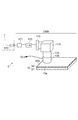
- FIG. 3 is a diagram showing a configuration of a first embodiment (first structure) of a laser processing apparatus suitably used in the laser processing method according to the present embodiment.
- the laser processing apparatus 1 according to the first embodiment includes a seed light source 100, a YbDF 110, a band pass filter 120, a YbDF 130, a band pass filter 140, a YbDF 150, a YbDF 160, and the like, and a MOPA structure is configured by these elements.
- the laser processing apparatus 1 outputs a pulse laser beam having a wavelength of about 1060 nm suitable for laser processing, specifically, 1040 nm to 1150 nm.
- the seed light source 100 includes a semiconductor laser that can be directly modulated, and pulse laser light is output from the semiconductor laser.
- the semiconductor laser is preferably a Fabry-Perot laser from the viewpoint of high power and from the viewpoint of avoiding nonlinear effects such as stimulated Brillouin scattering (SBS).
- SBS stimulated Brillouin scattering
- this semiconductor laser outputs pulsed laser light having a wavelength of about 1060 nm at which YbDFs 20, 40, and 50, which are amplification optical fibers, have a gain.
- YbDFs 110, 130, 150, and 160 are optical elements that amplify pulse laser light having a wavelength of about 1060 nm output from the seed light source 100, and Yb element is added as an active substance to the core of the optical fiber made of glass. Is obtained.
- the YbDFs 110, 130, 150, and 160 are advantageous in that the pumping light wavelength and the amplified light wavelength are close to each other and the power conversion efficiency is high.
- YbDFs 110, 130, 150, and 160 are advantageous in that they have a high gain in the vicinity of a wavelength of 1060 nm.
- These YbDFs 110, 130, 150, and 160 constitute a four-stage optical fiber amplifier.
- the first stage YbDF 110 is supplied with pumping light output from the pumping light source 112 and sequentially passing through the optical coupler 113 and the optical coupler 111 in the forward direction. Further, the YbDF 110 amplifies the pulsed laser light output from the seed light source 100 and passed through the optical isolator 114 and the optical coupler 111 in order. The pulse laser beam amplified by the YbDF 110 is output through the optical isolator 115.
- the band-pass filter 120 receives the pulsed laser light that has been amplified in the first stage YbDF 110 and then passed through the optical isolator 115, and attenuates a component in a specific wavelength band out of the wavelength band of the input pulsed laser light.
- the second stage YbDF 130 is supplied with pumping light output from the pumping light source 112 and sequentially passing through the optical coupler 113 and the optical coupler 131 in the forward direction. Further, the YbDF 130 amplifies the pulse laser beam output from the band pass filter 120 and passed through the optical isolator 131.
- the band pass filter 140 receives the pulse laser beam amplified in the second stage YbDF 130, and attenuates a component in a specific wavelength band in the wavelength band of the input pulse laser beam.
- the third stage YbDF 150 is supplied with pumping light output from the pumping light source 152 and passing through the optical coupler 151 in the forward direction. Further, the YbDF 150 amplifies the pulsed laser light output from the bandpass filter 140 and passed through the optical isolator 153.
- the fourth stage YbDF 160 is supplied with the pumping light output from the pumping light sources 162 to 166 and passing through the combiner 161 in the forward direction. Further, the YbDF 160 amplifies the pulse laser light amplified in the third stage YbDF 150 and sequentially passing through the optical isolator 167 and the combiner 161. The pulse laser beam amplified by the YbDF 160 is output to the outside of the laser processing apparatus (laser light source) via the end cap 170.
- the first stage YbDF110 is a single clad Al co-doped silica-based YbDF, 5 wt% Al concentration, 10 ⁇ m core diameter, 125 ⁇ m clad diameter, 70 dB / m 915 nm band excitation light unsaturated absorption, 240 dB / m 975 nm excitation light unsaturated absorption peak, and a fiber length of 7 m.
- the second stage YbDF 130 is a single clad Al co-doped silica-based YbDF, 5 wt% Al concentration, 10 ⁇ m core diameter, 125 ⁇ m cladding diameter, 70 dB / m 915 nm band excitation light unsaturated absorption, 240 dB / m 975 nm excitation light unsaturated absorption peak, and a fiber length of 7 m.
- the third stage YbDF150 is a double clad phosphate glass-based YbDF, with a P concentration of 26.4 wt%, an Al concentration of 0.8 wt%, a core diameter of 10 ⁇ m, an outer diameter of 125 ⁇ m, and its cross-sectional shape is It has an octagonal first cladding diameter, 1.8 dB / m 915 nm band excitation light unsaturated absorption, and a fiber length of 3 m.
- the fourth stage YbDF160 is a double clad Al co-doped silica-based YbDF, 5 wt% Al concentration, 10 ⁇ m core diameter, 125 ⁇ m clad diameter, 80 dB / m 915 nm band excitation light unsaturated absorption, 3.5 m Fiber length.
- the wavelengths of the excitation light supplied to YbDF110, 130, 150, 160 are all in the 0.975 ⁇ m band.
- the excitation light supplied to the YbDF 110 is single mode light with a power of 200 mW.
- the excitation light supplied to the YbDF 130 is single mode light with a power of 200 mW.
- the excitation light supplied to the YbDF 150 is multimode light with a power of 2W.
- the excitation light supplied to the YbDF 160 is multimode light with a power of 14 W.
- a Fabry-Perot type semiconductor laser is applied as the seed light source 100.
- the center wavelength of the bandpass filter 120 provided at the rear stage of the seed light source 100 is a graph shown in each area.
- the full width at half maximum of the pulsed laser beam can be compressed from about 5 ns to 0.5 ns by adjusting to be in the state of C2 or C3.
- Region (a) in FIG. 4 shows a pulse waveform when the output pulse of the seed light source 100 is deformed by adjusting the center wavelength of the band-pass filter 120 provided at the subsequent stage of the seed light source 100.
- Region (b) in FIG. 4 shows the spectrum in that case.
- region (c) of FIG. 4 is the figure which expanded a part of area
- a graph C1 shown in each region shows a case where there is no bandpass filter.
- Graphs C2 to C7 show the case where the center wavelength of the bandpass filter 120 is gradually changed from the long wavelength side to the short wavelength side.
- the center wavelength of the bandpass filter 120 is significantly detuned from the center wavelength of the spectrum of the seed light source 100 as shown in the graphs C2 and C3, the ASE generated in the downstream YbDF increases.
- the full width at half maximum of the transmission spectrum of each of the bandpass filters 120 and 140 is 3 nm.
- 5 and 6 are diagrams schematically showing how the ASE is removed by the band-pass filters 120 and 140 in the laser processing apparatus 1 (FIG. 3).
- the center wavelength of the transmission spectrum of band-pass filter 120 (D1 in region (a) and region (b) in FIG. 5) is the spectrum of output light from seed light source 10 (region (b in FIG. 5)).
- the power of the light output from the bandpass filter 120 (D3 in the region (b) in FIG. 5) can be kept high.
- the S / N ratio compared to the ASE component included in the light (D4 in the region (b) in FIG. 5) output from the YbDF 130 at the subsequent stage of the bandpass filter 120 can be kept high.
- the center wavelength of the transmission spectrum of band-pass filter 120 (E1 in regions (a) to (c) of FIG. 6) is the spectrum of the output light of seed light source 10 (FIG. 6).
- the peak wavelength of E2) in the area (a) is greatly deviated
- the power of the light output from the bandpass filter 120 (E3 in the area (b) in FIG. 6) is larger than that at the time of input. It will be attenuated.
- the S / N ratio compared to the ASE component included in the light (E4 in the region (b) and region (c) in FIG. 6) output from the YbDF 130 at the subsequent stage of the bandpass filter 120 is significantly deteriorated. To do.
- the S / N ratio of the light (E5 in the region (c) of FIG. 6) output from the bandpass filter 120 is improved by inserting a bandpass filter 140 further downstream of the YbDF 130. be able to.
- the center wavelength of the bandpass filter 140 is preferably set closer to the peak wavelength of the output spectrum of the seed light source 10 than the center wavelength of the bandpass filter 120.
- a phosphate glass-based YbDF whose ASE band is narrower than the Al-codoped quartz-based YbDF is applied to the third-stage YbDF150.
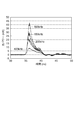
- FIG. 7 shows pulse waveforms with repetition frequencies of 100 kHz, 166.7 kHz, 200 kHz, 312.5 kHz, 500 kHz, 1 MHz, and 2.5 MHz.
- a space attenuator with an attenuation of about 65 dB is inserted after the end cap 170 at the output end of the laser processing apparatus 1, and the output light from the end cap 170 is converted into a Thorlabs photoelectric conversion module (SIR 5 -FC type) and the electric output waveform from the photoelectric conversion module was observed with an oscilloscope (DL9240) manufactured by Yokogawa Electric Corporation.
- FIG. 8 is a diagram showing the relationship between the repetition frequency of the output pulse laser beam of the laser processing apparatus 1 and the pulse energy. As shown in FIG. 8, the pulse energy of the output pulse laser beam was 0.041 mJ at the maximum. This operating state will be referred to as mode 1 for convenience in the future.
- FIG. 9 is a diagram showing a pulse waveform of the output pulse laser beam of the laser processing apparatus 1 in mode 2.
- FIG. 10 is a diagram showing the relationship between the repetition frequency of the output pulse laser beam of the laser processing apparatus 1 in mode 2 and the pulse energy.
- the full width at half maximum of the pulse is 18 ns when the repetition frequency is 500 kHz.
- the full width at half maximum of the pulse is caused by the transient response of the optical fiber amplifier. Becomes smaller.
- the pulse energy is a maximum of 0.24 mJ, which is about 6 times that in the mode 1.
- FIG. 11 shows the configuration of the laser processing apparatus 2 according to the second embodiment for realizing such an experiment.
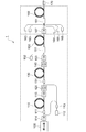
- the laser processing apparatus 2 according to the second embodiment uses the laser processing apparatus 1 according to the first embodiment described above as a laser light source, and further includes an illumination optical system 200a.
- the irradiation optical system from the end cap 170 of the laser processing apparatus 1 (laser light source) to the object includes a collimator 171 having an outgoing beam diameter of 1.6 mm, a polarization-independent isolator 172, a beam expander 173 having a magnification of 8 times, in order.
- a galvano scanner 174 and a telecentric F ⁇ lens 175 are included. When the pulse laser beam output from the end cap 170 passes through these optical elements, the transmittance of the pulse laser beam is 75%.
- the focal length of the F ⁇ lens is 164 mm.
- the spot area of the laser beam on the object is 2.35 ⁇ 10 ⁇ 6 cm 2 .
- the galvano scanner 174 irradiates the surface of the object 10 with the pulse laser beam P through the F ⁇ lens 175 while sweeping along the direction indicated by the arrow S1 from the sweep start point P1.
- the object 10 has a laminated structure including at least a conductor layer 11 and an insulating layer 12 provided so as to be in direct contact with the surface 11 a of the conductor layer 11. Further, the center of the pulsed laser beam P irradiated on the surface 12a of the insulating layer 12 is within the processing area AS along the direction indicated by the arrow S1 from the starting point P1, as shown in the area (b) of FIG. Swept in a spiral. Further, as shown in the area (c) of FIG.
- the centers P1a and P1b of the adjacent pulse laser beams P (the centers of the pulse laser beams move in the direction indicated by the arrow S2)
- a predetermined overlap rate (preferably 40% to 90%) is satisfied so as to overlap.
- the spiral sweep pattern is shown by the area
- an arbitrary beam sweep pattern such as a sweep pattern composed of only a linear component or a sweep pattern composed of a combination of a curve component and a linear component can be set.
- the insulating layer 12 is positioned in the removed portion (corresponding to the processing region AS).
- the surface 11a of the conductor layer 11 to be exposed can be exposed.
- auxiliary combustion gas such as oxygen as an assist gas
- processing region AS irradiation region of the pulse laser beam
- high efficiency is required for drilling a printed circuit board, and as described above (see paragraph “0035” of the present specification), in most cases, high-speed beam sweeping using a galvano scanner 174 and a telecentric F ⁇ lens 175 is required. is there. In this case, since the beam spot of the pulse laser beam moves at a high speed, it is impossible to spray the auxiliary combustion gas only on the beam spot.
- a wind tunnel 176 is installed directly below the F ⁇ lens 175 (between the F ⁇ lens 175 and the surface 12a of the insulating layer 12), and a combustion gas ( A structure for injecting O 2 ) is provided.
- the laser processing apparatus 3 according to the third embodiment has substantially the same configuration as the laser processing apparatus 2 according to the second embodiment, but structurally, an F ⁇ lens. 175 and the surface 12a of the insulating layer 12 are different in that a wind tunnel 176 is provided.
- FIG. 13 is a graph showing the relationship between the full width at half maximum of the pulse and the fluence per pulse in mode 1 and mode 2, respectively.
- mode 1 data is indicated by ⁇
- mode 2 data is indicated by ⁇ .
- mode 2A data to be described later is indicated by ⁇ .
- the relationship “the fluence destruction threshold is proportional to the square root of the pulse width” described in paragraph “0005” of Patent Document 3 is indicated by a broken line.
- the fluence per one pulse becomes 77j / cm 2 at maximum in mode 1 13J / cm 2, and the a maximum in mode 2.
- the printed circuit board 10 While the pulse laser light of mode 1 and mode 2 is swept at an overlap rate of 88% when the repetition frequency is 100 kHz, the printed circuit board 10 whose cross-sectional structure is shown in FIG. Via hole processing was performed by irradiating 12 objects).
- This printed circuit board 10 is formed by laminating a copper foil 11 having a thickness of 18 ⁇ m (corresponding to the region (a) in FIG. 11 and the conductor layer in FIG. 12), a polyimide resin layer 12b having a thickness of 14 ⁇ m, and a copper foil 13 having a thickness of 18 ⁇ m. Has a structured.
- the printed circuit board 10 also includes an adhesive layer (TPI) that adheres the layers 11, 12 b, and 13.
- TPI adhesive layer
- the polyimide resin layer 12b and the adhesive layer constitute the insulating layer 12 (corresponding to the region (a) in FIG. 11 and the insulating layer in FIG. 12).
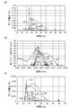
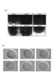
- the copper foil 13 of the printed circuit board 10 is previously punched by chemical processing or laser processing. The results of this via hole processing are shown in FIGS. 15 and 16.
- FIG. 15 and FIG. 16 are a photograph and an SEM photograph of the Via hole observed with an optical microscope when the pulse is changed at repetition frequencies of 500, 400, 312.5, 200, 166.7, and 100 kHz in mode 1, respectively.
- FIG. 15 shows the results when processing in normal air without using an assist gas.
- FIG. 16 shows the results when processing while blowing oxygen gas as the assist gas.
- region (a) of each of FIG. 15 and FIG. 16 shows an optical micrograph
- region (b) of FIG. 15 and FIG. 16 shows a SEM photograph.
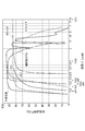
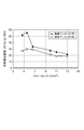
- FIG. 17 is a graph showing the relationship between the fluence per pulse at the above-mentioned repetition frequency in mode 1 and the detected concentration of carbon remaining at the bottom of the Via hole.
- EDX energy dispersive X-ray fluorescence analyzer
- smear a processing residue remaining in the form of a film or island on the surface of the conductor layer
- smear is the heat conductivity of the pulse laser beam irradiation.
- the maximum power that is instantaneously irradiated that is, the irradiation intensity at the pulse peak, simultaneously with the fluence.
- the oxygen assist gas when used, the insulating layer 12 is successfully removed at an irradiation intensity of 18 GW / cm 2 or more.
- the insulating layer 12 is successfully removed if the irradiation intensity is 24 GW / cm 2 or more.
- These threshold values of the irradiation intensity are considered to depend on the material and thickness of the conductor layer 11 and also on the material of the stage on which the conductor layer 11 is placed. It seems to be necessary.
- the material of the upper surface of the stage on which the printed circuit board 10 is installed is preferably not a highly heat conductive metal or the like, but a ceramic or glass having a low heat conductivity.
- the mode 2A of FIG. A removal area is swept using a pulse having a high fluence, and a beam sweep in the processing area AS as shown in the area (b) of FIG.
- the latter stage of sweeping that is, in the smear removal stage, if mode 1 is applied which is excellent in maximum irradiation intensity and fluence is suppressed, and beam sweep is performed over the entire processing area AS (removal area) It is expected that both the time spent for removing the insulating layer 12 and the damage to the conductor layer 11 can be minimized.
- both can be processed with a single laser.
- FIG. 18 An example of the beam sweep pattern at this time is shown in FIG.
- a region (a) in FIG. 18 shows the inside of a hole having a diameter of 50 ⁇ m (a hole formed in advance in the conductor layer 13 and its bottom corresponds to the processing region AS) by the arrow S3 from the sweep start point P1.
- An Archimedes spiral beam sweep pattern (corresponding to one beam sweep) directed toward the sweep end point P2 (the center of the processing region AS) along the direction is shown.
- the region (b) in FIG. 18 moves from the sweep start point P1 to the center of the machining area AS along the direction indicated by the arrow S4.
- a beam sweep pattern from the center of the machining area AS toward the sweep end point P2 along the direction indicated by the arrow S5 is shown.
- the beam sweep pattern in the region (a) in FIG. 18 performs only the beam sweep in the mode 2A (described later) during one beam sweep from the sweep start point P1 to the sweep end point P2.
- the beam sweep pattern in the region (b) in FIG. 18 has twice the radius change amount as the beam sweep pattern shown in the region (a) in FIG.
- the beam sweep in the mode 2A is performed in the first half (from the sweep start point P1 to the center of the processing region AS) in one beam sweep, while the second half (processing region)
- the beam sweep in the mode 1 is performed from the center of the AS to the sweep end point P2.
- the number of pulse shots in the machining area AS is 100.
- the processing is not successful unless the pulse width is set to 10 ps or less. As shown in FIG. 7, the processing is performed even when the full width at half maximum of the pulse is about 0.6 ns. Therefore, a special pulse compression method in the optical amplifying unit such as CPA is unnecessary.
- each of the polyimide resin layer 12b and the adhesive layer (which constitutes the insulating layer 12 and can be smeared) constituting the printed circuit board 10 has various compositions and is not necessarily a short pulse as in mode 1.
- the insulating layer 12 can be removed.
- the modulation current pulse width of the seed light source 100 in mode 2 is 5 ns
- the output pulse waveform is as shown in FIG. 19, and the full width at half maximum of the pulse is about 2 ns at a repetition frequency of 100 to 400 kHz.
- this operation is referred to as mode 2A.
- the irradiation optical system 200b of the laser processing apparatus 3 uses oxygen gas as an assist gas, irradiates a printed circuit board with pulsed laser light, and performs via hole processing.
- oxygen gas as an assist gas
- the EDX detection concentration of carbon is about 20 At.% Or less (in the best case, 0 At. %) And can. At this time, the surface of the conductor layer is hardly damaged.
- the carbon EDX The detected concentration was 20 At. %.
- the fluence per pulse is high, or it is desirable that the repetition frequency is high (300 kHz or more, that is, the overlap rate is 96%) even if the fluence per pulse is low. There is also.
- the pulse width was 5 ns or more, good results were not obtained regardless of the repetition frequency.
- the insulating layer portion that is in contact with the conductor is smeared as described above, heat easily escapes to the conductor even if it is irradiated with a laser. Therefore, a higher peak power in a shorter time (as shown in FIG. As described above, it is considered that it is desirable to concentrate and heat the object to be processed at 7.5 kW or more.
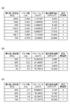
- FIG. 20 is a table summarizing the relationship between the repetition frequency, pulse width, and fluence in each of mode 1, mode 2, and mode 2A.
- area (a) shows the case of mode 1
- area (b) shows the case of mode 2
- area (c) shows the case of mode 1A.
- the example numbers when the processing of the insulating layer 12 is successful are shown.
- Example 1 and Example 2 are matched and shown in FIG.
- selective laser removal of the insulating layer in a printed circuit board or a composite material composed of a conductor layer and an insulating layer in a wavelength range that originally transmits the insulating layer is not necessarily performed using copper and a polyimide resin.
- the selective removal process is good even when an alloy mainly composed of gold (Au), aluminum (Al) or the like is used for the conductor layer or the plating layer attached to the surface of the conductor layer. Is feasible.
- Laser processing device 200a, 200b ... Illumination optical system, 100 ... Seed light source, 110 ... YbDF, 111 ... Optical coupler, 112 ... Excitation light source, 113 ... Optical coupler, 114, 115 ... Optical isolator, 120 ... band pass filter, 130 ... YbDF, 131 ... optical coupler, 140 ... band pass filter, 150 ... YbDF, 151 ... optical coupler, 152 ... excitation light source, 153 ... optical coupler, 160 ... YbDF, 161 ...
- combiner 162 to 166, excitation light source, 167, optical isolator, 170, end cap, 171, collimator, 172, polarization-independent isolator, 173, beam expander, 174, galvano scanner, 175, telecentric F ⁇ lens 175, 176,. Wind tunnel.
Landscapes
- Physics & Mathematics (AREA)
- Optics & Photonics (AREA)
- Engineering & Computer Science (AREA)
- Plasma & Fusion (AREA)
- Mechanical Engineering (AREA)
- Manufacturing & Machinery (AREA)
- Microelectronics & Electronic Packaging (AREA)
- Electromagnetism (AREA)
- Laser Beam Processing (AREA)
- Production Of Multi-Layered Print Wiring Board (AREA)
Abstract
Description
Claims (12)
- 導体層と前記導体層上に積層された樹脂製の絶縁層とを含む対象物をパルスレーザ光の光路上に設置し、前記対象物にパルスレーザ光を照射することにより、前記絶縁層のうち前記導体層上の所定領域に位置する部分を除去するレーザ加工方法であって、
前記パルスレーザ光の波長として、前記導体層に対する吸収率が10%未満かつ前記絶縁層に対する透過率が70%以上となる波長が選択された前記パルスレーザ光を、前記絶縁層を通過した後に前記導体層に到達するよう、前記対象物の所定領域に照射するレーザ加工方法。 - 導体層と前記導体層上に積層された樹脂製の絶縁層とを含む対象物をパルスレーザ光の光路上に設置し、前記対象物にパルスレーザ光を照射することにより、前記絶縁層のうち前記導体層上の所定領域に位置する部分を除去するレーザ加工方法であって、
前記パルスレーザ光の波長として、前記導体層に対する吸収率が10%未満かつ前記絶縁層に対する透過率が70%以上となる波長を選択し、
前記絶縁層が除去された後の前記導体層表面における炭素検出濃度の許容レベルとの関係において、前記パルスレーザ光の1パルス当たりのフルーエンスを設定し、
前記パルスレーザ光の半値全幅が5ns未満となるように、前記パルスレーザ光の繰り返し周波数を設定し、
前記選択された波長、前記設定された1パルス当たりのフルーエンスおよび前記設定された繰り返し周波数を有する前記パルスレーザ光を、前記絶縁層を通過した後に前記導体層に到達するよう、前記対象物の所定領域に照射するレーザ加工方法。 - 前記絶縁層表面において、照射されたパルスレーザ光の照射スポットに対する次回照射されるパルスレーザ光の照射スポットのオーバーラップ率が40%~90%となるように、前記絶縁層表面に対して前記パルスレーザ光を掃引させながら照射することを特徴とする請求項1または2記載のレーザ加工方法。
- 前記パルスレーザ光の波長は、希土類元素を含む光活性媒質を用いたレーザ光源から直接出力し得る波長であることを特徴とする請求項1または2記載のレーザ加工方法。
- 前記光活性媒質は、Yb添加光ファイバであることを特徴とする請求項4記載のレーザ加工方法。
- 前記パルスレーザ光の半値全幅は、前記絶縁層の加工残渣が前記導体層表面に膜状または島状に残らない程度に設定されることを特徴とする請求項1または2記載のレーザ加工方法。
- 前記パルスレーザ光の半値全幅は、5ns未満であることを特徴とする請求項1記載のレーザ加工方法。
- 前記パルスレーザ光の半値全幅は、10psより大きいことを特徴とする請求項1または2記載のレーザ加工方法。
- 前記パルスレーザ光のパルスピークにおける照射強度は、前記絶縁層の加工残渣が前記導体層表面に膜状または島状に残らない程度に設定されていることを特徴とする請求項1または2記載のレーザ加工方法。
- 請求項1~9のいずれか一項記載のレーザ加工方法を実行するレーザ加工装置であって、
当該レーザ加工装置は、前記パルスレーザ光を生成するレーザ光源と、前記パルスレーザ光が到達する前記絶縁層表面の加工領域内において、前記パルスレーザ光をビーム掃引する照射光学系とを備えるとともに、
前記レーザ光源は、前記加工領域内において任意のパターンを描きながら掃引始点から掃引終点に向かうビーム掃引を一単位とするとき、この一単位のビーム掃引の期間中、前記パルスレーザ光の生成条件のうち、パルス幅および繰返し周波数の少なくともいずれかを、1回またはそれ以上変更し、
前記レーザ光源は、前記一単位のビーム掃引における掃引開始時点を含むビーム掃引初期の前記パルスレーザ光の1パルス当たりのフルーエンスを、前記ビーム掃引初期以降の期間における前記パルスレーザ光の1パルス当たりのフルーエンスより大きく設定することを特徴とするレーザ加工装置。 - 前記レーザ光源は、前記一単位のビーム掃引における掃引終了時点を含むビーム掃引終期の前記パルスレーザ光のパルスピークにおける照射強度を、前記ビーム掃引終期以前の期間における前記パルスレーザ光のパルスピークにおける照射強度よりも大きく設定することを特徴とする請求項10記載のレーザ加工装置。
- 前記照射光学系は、前記絶縁層表面において、照射されたパルスレーザ光のビームスポットに対する次回照射されるパルスレーザ光のビームスポットのオーバーラップ率が40%~90%となるように、前記絶縁層表面に対して前記パルスレーザ光を掃引させながら照射することを特徴とする請求項10または11記載のレーザ加工装置方法。
Priority Applications (3)
| Application Number | Priority Date | Filing Date | Title |
|---|---|---|---|
| US13/059,592 US8628715B2 (en) | 2008-10-23 | 2009-10-23 | Laser processing method and laser processing device |
| EP09822081.7A EP2366487B1 (en) | 2008-10-23 | 2009-10-23 | Laser processing method and laser processing device |
| CN200980142278.XA CN102196880B (zh) | 2008-10-23 | 2009-10-23 | 激光加工方法以及激光加工装置 |
Applications Claiming Priority (2)
| Application Number | Priority Date | Filing Date | Title |
|---|---|---|---|
| JP2008273341 | 2008-10-23 | ||
| JP2008-273341 | 2008-10-23 |
Publications (1)
| Publication Number | Publication Date |
|---|---|
| WO2010047384A1 true WO2010047384A1 (ja) | 2010-04-29 |
Family
ID=42119421
Family Applications (1)
| Application Number | Title | Priority Date | Filing Date |
|---|---|---|---|
| PCT/JP2009/068240 Ceased WO2010047384A1 (ja) | 2008-10-23 | 2009-10-23 | レーザ加工方法およびレーザ加工装置 |
Country Status (6)
| Country | Link |
|---|---|
| US (1) | US8628715B2 (ja) |
| EP (1) | EP2366487B1 (ja) |
| JP (2) | JP5454080B2 (ja) |
| KR (1) | KR101601344B1 (ja) |
| CN (1) | CN102196880B (ja) |
| WO (1) | WO2010047384A1 (ja) |
Families Citing this family (19)
| Publication number | Priority date | Publication date | Assignee | Title |
|---|---|---|---|---|
| KR20130037209A (ko) * | 2010-06-04 | 2013-04-15 | 이비덴 가부시키가이샤 | 배선판의 제조 방법 |
| JP5983407B2 (ja) * | 2010-09-15 | 2016-08-31 | 住友電気工業株式会社 | レーザ加工方法 |
| CN102240846B (zh) * | 2011-06-17 | 2015-01-14 | 山西飞虹激光科技有限公司 | 全光纤结构线偏振脉冲光纤激光加工装置 |
| JP5920662B2 (ja) * | 2012-06-05 | 2016-05-18 | 三菱マテリアル株式会社 | レーザ加工装置およびレーザ加工方法 |
| JP5920661B2 (ja) * | 2012-06-05 | 2016-05-18 | 三菱マテリアル株式会社 | レーザ加工装置およびレーザ加工方法 |
| KR20150097475A (ko) * | 2012-12-20 | 2015-08-26 | 일렉트로 싸이언티픽 인더스트리이즈 인코포레이티드 | 레이저 미세기계가공에 의한 이미지 형성 방법 |
| US9950392B2 (en) | 2014-03-04 | 2018-04-24 | Rohr, Inc. | Forming one or more apertures in a fiber-reinforced composite object with a laser |
| WO2016084374A1 (ja) * | 2014-11-28 | 2016-06-02 | 日本ゼオン株式会社 | デスミア処理方法および多層プリント配線板の製造方法 |
| CN104810721B (zh) * | 2015-03-02 | 2017-11-03 | 吕志伟 | 基于受激布里渊散射脉宽压缩的高能量数百皮秒激光装置 |
| JP6762024B2 (ja) * | 2016-07-28 | 2020-09-30 | 三星ダイヤモンド工業株式会社 | レーザ加工装置及びレーザ加工方法 |
| JP6508153B2 (ja) * | 2016-09-21 | 2019-05-08 | 日亜化学工業株式会社 | 発光素子の製造方法 |
| CN106271089B (zh) * | 2016-09-30 | 2019-01-25 | 英诺激光科技股份有限公司 | 一种激光薄膜刻蚀装置及方法 |
| CN110691671B (zh) * | 2017-04-20 | 2023-10-10 | 西尔特克特拉有限责任公司 | 用于具有限定地定向的改性线的晶片制造的方法 |
| KR102450776B1 (ko) * | 2017-10-27 | 2022-10-05 | 삼성전자주식회사 | 레이저 가공 방법, 기판 다이싱 방법 및 이를 수행하기 위한 기판 가공 장치 |
| CN108448372B (zh) * | 2018-05-22 | 2024-04-02 | 中国人民解放军国防科技大学 | 集成化光纤器件及其光纤放大器 |
| CA3176138A1 (en) * | 2020-03-31 | 2021-10-07 | Honda Motor Co., Ltd. | Laser machining method |
| DE102020212087A1 (de) * | 2020-09-25 | 2022-03-31 | Trumpf Laser- Und Systemtechnik Gmbh | Mehrstufiges Laser-Entlacken eines stabförmigen Leiters |
| JP7596842B2 (ja) * | 2021-02-19 | 2024-12-10 | トヨタ自動車株式会社 | 配線基板の製造方法 |
| KR102688890B1 (ko) * | 2022-07-06 | 2024-07-26 | 케이투레이저시스템 (주) | 라인빔 레이저 용접 장치 레이저 및 이의 용접 방법 |
Citations (3)
| Publication number | Priority date | Publication date | Assignee | Title |
|---|---|---|---|---|
| JP2002035976A (ja) * | 2000-07-24 | 2002-02-05 | Sumitomo Heavy Ind Ltd | 紫外レーザを用いた孔開け方法 |
| JP2003001464A (ja) * | 2001-06-22 | 2003-01-08 | Nippei Toyama Corp | レーザ加工装置及びレーザ加工方法 |
| JP2008211084A (ja) * | 2007-02-27 | 2008-09-11 | Toshiba Corp | レーザ加工装置 |
Family Cites Families (30)
| Publication number | Priority date | Publication date | Assignee | Title |
|---|---|---|---|---|
| US5656186A (en) * | 1994-04-08 | 1997-08-12 | The Regents Of The University Of Michigan | Method for controlling configuration of laser induced breakdown and ablation |
| US5866911A (en) * | 1994-07-15 | 1999-02-02 | Baer; Stephen C. | Method and apparatus for improving resolution in scanned optical system |
| US5593606A (en) * | 1994-07-18 | 1997-01-14 | Electro Scientific Industries, Inc. | Ultraviolet laser system and method for forming vias in multi-layered targets |
| JPH10341069A (ja) * | 1997-06-05 | 1998-12-22 | Nec Corp | ビアホール形成方法 |
| JP2002335063A (ja) * | 2001-05-09 | 2002-11-22 | Hitachi Via Mechanics Ltd | プリント基板の穴あけ加工方法および装置 |
| TW503143B (en) * | 2000-10-06 | 2002-09-21 | Hitachi Via Mechanics Ltd | Method and apparatus for drilling printed wiring boards |
| JP4373596B2 (ja) | 2000-10-06 | 2009-11-25 | 日立ビアメカニクス株式会社 | プリント基板の加工方法 |
| GB2377664A (en) | 2001-06-22 | 2003-01-22 | Nippei Toyama Corp | Laser beam machining apparatus and laser beam machining method |
| JP4006247B2 (ja) * | 2002-03-08 | 2007-11-14 | 住友重機械工業株式会社 | レーザ加工方法及びレーザ加工装置 |
| JP2003347747A (ja) * | 2002-05-30 | 2003-12-05 | Toppan Printing Co Ltd | 多層配線基板の製造方法およびこれを用いた多層配線基板 |
| JP4174267B2 (ja) * | 2002-08-21 | 2008-10-29 | 日立ビアメカニクス株式会社 | レーザ加工方法 |
| WO2004026522A1 (en) * | 2002-09-19 | 2004-04-01 | Gert Jan Huizinga | Method for laser working a film material and film material to be worked using that method. |
| JP2004223533A (ja) * | 2003-01-21 | 2004-08-12 | Sumitomo Heavy Ind Ltd | レーザ加工方法 |
| JP2004327830A (ja) * | 2003-04-25 | 2004-11-18 | Sumitomo Heavy Ind Ltd | プリント基板の製造方法およびプリント基板 |
| JP2004351513A (ja) * | 2003-05-30 | 2004-12-16 | Toppan Printing Co Ltd | 超短パルスレーザーによる材料加工方法、プリント配線板、及びその製造方法 |
| JP2005342749A (ja) * | 2004-06-01 | 2005-12-15 | Hitachi Via Mechanics Ltd | レーザ加工方法 |
| JP4252939B2 (ja) * | 2004-07-09 | 2009-04-08 | 住友重機械工業株式会社 | レーザ加工方法 |
| TWI382795B (zh) * | 2005-03-04 | 2013-01-11 | 日立比亞機械股份有限公司 | A method of opening a printed circuit board and an opening device for a printed circuit board |
| JP4764989B2 (ja) * | 2005-04-28 | 2011-09-07 | 富士電機株式会社 | レーザ加工方法 |
| JP2007021528A (ja) * | 2005-07-15 | 2007-02-01 | Matsushita Electric Ind Co Ltd | レーザ加工装置およびその調整方法 |
| JP4762671B2 (ja) * | 2005-10-26 | 2011-08-31 | 古河電気工業株式会社 | ダイシングテープ、および半導体ウェハダイシング方法 |
| GB0524031D0 (en) * | 2005-11-25 | 2006-01-04 | Univ Heriot Watt | High resolution cold processing of ceramics |
| KR100744545B1 (ko) * | 2005-12-12 | 2007-08-01 | 한국전자통신연구원 | 중적외선 파장대 완전 광섬유 레이저 소자 |
| US20080093775A1 (en) * | 2006-08-19 | 2008-04-24 | Colorado State University Research Foundation | Nanometer-scale ablation using focused, coherent extreme ultraviolet/soft x-ray light |
| US8546067B2 (en) * | 2008-03-21 | 2013-10-01 | The Board Of Trustees Of The University Of Illinois | Material assisted laser ablation |
| JP5281922B2 (ja) * | 2009-02-25 | 2013-09-04 | 浜松ホトニクス株式会社 | パルスレーザ装置 |
| EP2414130B2 (en) * | 2009-03-30 | 2019-04-24 | Boegli-Gravures S.A. | Method and device for structuring a solid body surface with a hard coating with a first laser with pulses in the nanosecond field and a second laser with pulses in the pico- or femtosecond field ; packaging foil |
| US8435437B2 (en) * | 2009-09-04 | 2013-05-07 | Abbott Cardiovascular Systems Inc. | Setting laser power for laser machining stents from polymer tubing |
| EP2336823A1 (de) * | 2009-12-18 | 2011-06-22 | Boegli-Gravures S.A. | Verfahren und Vorrichtung zur Herstellung von Masken für eine Laseranlage zur Erzeugung von Mikrostrukturen. |
| JP6055414B2 (ja) * | 2010-10-22 | 2016-12-27 | エレクトロ サイエンティフィック インダストリーズ インコーポレーテッド | ビームディザリング及びスカイビングのためのレーザ加工システム並びに方法 |
-
2009
- 2009-10-22 JP JP2009243683A patent/JP5454080B2/ja not_active Expired - Fee Related
- 2009-10-23 WO PCT/JP2009/068240 patent/WO2010047384A1/ja not_active Ceased
- 2009-10-23 EP EP09822081.7A patent/EP2366487B1/en not_active Not-in-force
- 2009-10-23 US US13/059,592 patent/US8628715B2/en not_active Expired - Fee Related
- 2009-10-23 CN CN200980142278.XA patent/CN102196880B/zh not_active Expired - Fee Related
- 2009-10-23 KR KR1020117011686A patent/KR101601344B1/ko not_active Expired - Fee Related
-
2013
- 2013-12-25 JP JP2013266688A patent/JP5804040B2/ja not_active Expired - Fee Related
Patent Citations (3)
| Publication number | Priority date | Publication date | Assignee | Title |
|---|---|---|---|---|
| JP2002035976A (ja) * | 2000-07-24 | 2002-02-05 | Sumitomo Heavy Ind Ltd | 紫外レーザを用いた孔開け方法 |
| JP2003001464A (ja) * | 2001-06-22 | 2003-01-08 | Nippei Toyama Corp | レーザ加工装置及びレーザ加工方法 |
| JP2008211084A (ja) * | 2007-02-27 | 2008-09-11 | Toshiba Corp | レーザ加工装置 |
Non-Patent Citations (1)
| Title |
|---|
| See also references of EP2366487A4 * |
Also Published As
| Publication number | Publication date |
|---|---|
| EP2366487A4 (en) | 2014-09-24 |
| CN102196880B (zh) | 2014-06-18 |
| US8628715B2 (en) | 2014-01-14 |
| JP5454080B2 (ja) | 2014-03-26 |
| KR101601344B1 (ko) | 2016-03-08 |
| US20110148002A1 (en) | 2011-06-23 |
| JP2010120084A (ja) | 2010-06-03 |
| JP5804040B2 (ja) | 2015-11-04 |
| JP2014121734A (ja) | 2014-07-03 |
| EP2366487B1 (en) | 2015-05-20 |
| CN102196880A (zh) | 2011-09-21 |
| EP2366487A1 (en) | 2011-09-21 |
| KR20110086118A (ko) | 2011-07-27 |
Similar Documents
| Publication | Publication Date | Title |
|---|---|---|
| JP5454080B2 (ja) | レーザ加工方法およびレーザ加工装置 | |
| US6979798B2 (en) | Laser system and method for material processing with ultra fast lasers | |
| US7724787B2 (en) | Method and system for tunable pulsed laser source | |
| US9321126B2 (en) | Laser-based material processing apparatus and methods | |
| US7428253B2 (en) | Method and system for a pulsed laser source emitting shaped optical waveforms | |
| CN101501943B (zh) | 光纤放大器和具有减少的带外增益的光纤激光器 | |
| JP5675769B2 (ja) | 短レーザパルスのテイラードバーストによるレーザマイクロマシニング | |
| CN101448603A (zh) | 以短脉冲,固态紫外线激光做微加工 | |
| JPWO2008143084A1 (ja) | ファイバレーザ | |
| JP2012515450A (ja) | 微細加工用のパルス時間プログラマブル超高速バーストモードレーザ | |
| JP5983407B2 (ja) | レーザ加工方法 | |
| JP5578935B2 (ja) | ファイバレーザ加工装置 | |
| JP4732120B2 (ja) | 光増幅用光ファイバの製造方法 | |
| JP2006145584A (ja) | 波長が紫外域の複数のレーザの形成方法および形成装置並びにレーザ加工装置 | |
| JP2007221037A (ja) | 光増幅器、ファイバレーザ及び反射光除去方法 | |
| Kong et al. | High energy multi-mode nanosecond pulsed fiber amplifier based on the 940 nm LD pumping with effective suppression of the ASE and the SRS effect | |
| JP2004087541A (ja) | 高出力光源装置 | |
| CN121282706A (zh) | 一种模场适配器、集成激光器和集成激光器的制作方法 | |
| JP2003338796A (ja) | パルス光の波形制御方法及び光増幅装置 | |
| Melo et al. | Stimulated Raman scattering mitigation through amplified spontaneous emission simultaneous seeding on high power double-clad fiber pulse amplifiers |
Legal Events
| Date | Code | Title | Description |
|---|---|---|---|
| WWE | Wipo information: entry into national phase |
Ref document number: 200980142278.X Country of ref document: CN |
|
| 121 | Ep: the epo has been informed by wipo that ep was designated in this application |
Ref document number: 09822081 Country of ref document: EP Kind code of ref document: A1 |
|
| WWE | Wipo information: entry into national phase |
Ref document number: 13059592 Country of ref document: US |
|
| NENP | Non-entry into the national phase |
Ref country code: DE |
|
| WWE | Wipo information: entry into national phase |
Ref document number: 2009822081 Country of ref document: EP |
|
| ENP | Entry into the national phase |
Ref document number: 20117011686 Country of ref document: KR Kind code of ref document: A |