WO2010052901A1 - 周波数可変増幅器 - Google Patents
周波数可変増幅器 Download PDFInfo
- Publication number
- WO2010052901A1 WO2010052901A1 PCT/JP2009/005850 JP2009005850W WO2010052901A1 WO 2010052901 A1 WO2010052901 A1 WO 2010052901A1 JP 2009005850 W JP2009005850 W JP 2009005850W WO 2010052901 A1 WO2010052901 A1 WO 2010052901A1
- Authority
- WO
- WIPO (PCT)
- Prior art keywords
- signal
- injection
- main
- input signal
- amplifier system
- Prior art date
- Legal status (The legal status is an assumption and is not a legal conclusion. Google has not performed a legal analysis and makes no representation as to the accuracy of the status listed.)
- Ceased
Links
Images


Classifications
-
- H—ELECTRICITY
- H03—ELECTRONIC CIRCUITRY
- H03F—AMPLIFIERS
- H03F1/00—Details of amplifiers with only discharge tubes, only semiconductor devices or only unspecified devices as amplifying elements
- H03F1/42—Modifications of amplifiers to extend the bandwidth
-
- H—ELECTRICITY
- H03—ELECTRONIC CIRCUITRY
- H03F—AMPLIFIERS
- H03F1/00—Details of amplifiers with only discharge tubes, only semiconductor devices or only unspecified devices as amplifying elements
- H03F1/32—Modifications of amplifiers to reduce non-linear distortion
-
- H—ELECTRICITY
- H03—ELECTRONIC CIRCUITRY
- H03F—AMPLIFIERS
- H03F3/00—Amplifiers with only discharge tubes or only semiconductor devices as amplifying elements
- H03F3/189—High-frequency amplifiers, e.g. radio frequency amplifiers
- H03F3/19—High-frequency amplifiers, e.g. radio frequency amplifiers with semiconductor devices only
- H03F3/191—Tuned amplifiers
-
- H—ELECTRICITY
- H03—ELECTRONIC CIRCUITRY
- H03F—AMPLIFIERS
- H03F3/00—Amplifiers with only discharge tubes or only semiconductor devices as amplifying elements
- H03F3/20—Power amplifiers, e.g. Class B amplifiers, Class C amplifiers
- H03F3/21—Power amplifiers, e.g. Class B amplifiers, Class C amplifiers with semiconductor devices only
- H03F3/211—Power amplifiers, e.g. Class B amplifiers, Class C amplifiers with semiconductor devices only using a combination of several amplifiers
-
- H—ELECTRICITY
- H03—ELECTRONIC CIRCUITRY
- H03F—AMPLIFIERS
- H03F3/00—Amplifiers with only discharge tubes or only semiconductor devices as amplifying elements
- H03F3/20—Power amplifiers, e.g. Class B amplifiers, Class C amplifiers
- H03F3/24—Power amplifiers, e.g. Class B amplifiers, Class C amplifiers of transmitter output stages
-
- H—ELECTRICITY
- H03—ELECTRONIC CIRCUITRY
- H03F—AMPLIFIERS
- H03F2200/00—Indexing scheme relating to amplifiers
- H03F2200/192—A hybrid coupler being used at the input of an amplifier circuit
-
- H—ELECTRICITY
- H03—ELECTRONIC CIRCUITRY
- H03F—AMPLIFIERS
- H03F2200/00—Indexing scheme relating to amplifiers
- H03F2200/195—A hybrid coupler being used as power measuring circuit at the input of an amplifier circuit
-
- H—ELECTRICITY
- H03—ELECTRONIC CIRCUITRY
- H03F—AMPLIFIERS
- H03F2200/00—Indexing scheme relating to amplifiers
- H03F2200/198—A hybrid coupler being used as coupling circuit between stages of an amplifier circuit
-
- H—ELECTRICITY
- H03—ELECTRONIC CIRCUITRY
- H03F—AMPLIFIERS
- H03F2200/00—Indexing scheme relating to amplifiers
- H03F2200/201—A hybrid coupler being used as power measuring inter-stage circuit between two stages of an amplifier circuit
-
- H—ELECTRICITY
- H03—ELECTRONIC CIRCUITRY
- H03F—AMPLIFIERS
- H03F2200/00—Indexing scheme relating to amplifiers
- H03F2200/204—A hybrid coupler being used at the output of an amplifier circuit
-
- H—ELECTRICITY
- H03—ELECTRONIC CIRCUITRY
- H03F—AMPLIFIERS
- H03F2200/00—Indexing scheme relating to amplifiers
- H03F2200/207—A hybrid coupler being used as power measuring circuit at the output of an amplifier circuit
Definitions
- This invention relates to a variable frequency amplifier capable of matching at an arbitrary frequency.
- Wireless communication systems such as frequency and modulation system are diversified, and many wireless communication systems are mixed today.
- hardware is required for each frequency and modulation system, so that the size of the wireless device tends to increase. Therefore, a software defined radio capable of supporting a plurality of wireless communication systems by changing the frequency and modulation system by software is desired. With a software defined radio, it is not necessary to prepare hardware for each frequency and modulation method, so that the size of the radio can be reduced.
- the power amplifier mounted on the software defined radio needs to cover the entire frequency range defined by the software, and is required to operate over a wide frequency range.
- a method of switching the matching circuit of the power amplifier for each frequency has been proposed as a method for obtaining high efficiency characteristics, high output characteristics, and wideband characteristics. ing.
- Non-Patent Document 1 discloses an output matching circuit of a frequency variable amplifier (triple band power amplifier).
- a frequency variable amplifier triple band power amplifier
- two MEMS switches are turned ON / OFF according to the frequency.
- the configuration of the output matching circuit is switched so that matching can be achieved at three frequencies.
- variable frequency amplifier Since the conventional variable frequency amplifier is configured as described above, matching can be achieved at three frequencies by turning on and off two MEMS switches. However, in order to be able to achieve matching at more frequencies, it is necessary to mount a large number of switches that switch the matching state. For this reason, the configuration of the output matching circuit becomes complicated, and the loss increases to reduce the efficiency. Therefore, there is a problem that the number of frequencies that can be switched is practically limited.
- the present invention has been made to solve the above-described problems, and an object of the present invention is to obtain a frequency variable amplifier capable of matching at an arbitrary frequency without causing an increase in loss.
- variable frequency amplifier distributes the main amplification means for amplifying one of the input signals distributed by the signal distribution means and outputting the amplified signal, and the signal distribution means according to a set value given from the outside. And adjusting the amplitude or phase of the other input signal, and amplifying the input signal and injecting and amplifying the amplified signal to the output side of the main amplifying means. is there.
- the main amplification means for amplifying one input signal distributed by the signal distribution means and outputting the amplified signal, and the other distributed by the signal distribution means according to the set value given from the outside And adjusting the amplitude or phase of the input signal, and amplifying the input signal and injecting the amplified signal to the output side of the main amplifying means.
- FIG. 1 is a configuration diagram illustrating a variable frequency amplifier according to a first embodiment of the present invention.
- FIG. 2 is a schematic diagram relating to the operation of the frequency variable amplifier of FIG. 1. It is explanatory drawing which shows the calculation result of the input / output reflection characteristic of the main amplifier system. At 5.4 GHz, the output reflection characteristics at the main amplifier system end of the frequency variable amplifier when the phase shifter 10 and the attenuator 11 of the injection amplifier system 9 are set so that the output of the main amplifier system 4 is maximized. It is explanatory drawing which shows a calculation result. It is explanatory drawing which shows the calculation result of the frequency dependence of the output power of the main amplifier system 4 except the electric power of the signal inject
- FIG. 1 is a block diagram showing a variable frequency amplifier according to Embodiment 1 of the present invention.
- an input terminal 1 is a terminal for inputting a signal to be amplified.
- the directional coupler 2 is a distributor that distributes a signal input from the input terminal 1 (hereinafter referred to as “input signal”) to the directional coupler 3 and the power meter 16.
- the directional coupler 3 is a distributor that distributes the input signal distributed by the directional coupler 2 to the main amplifier system 4 and the injection amplifier system 9.
- the directional coupler 3 constitutes signal distribution means.
- the main amplifier system 4 is a balanced amplifier composed of 3 dB directional couplers 6 and 8 and unit amplifiers 7a and 7b, and is injected from the output side of the 3 dB directional coupler 8 which is an isolation port on the output side. While receiving the output signal of the amplifier system 9, one input signal distributed by the directional coupler 3 is amplified and the amplified signal is output to the output terminal 14.
- the main amplifier system 4 constitutes main amplification means.
- the isolation resistor 5 of the main amplifier system 4 is a resistor having one end grounded and the other end connected to the input side of the 3 dB directional coupler 6.
- the 3 dB directional coupler 6 is connected to the isolation resistor 5 and the directional coupler 3 on the input side, and distributes the input signal distributed by the directional coupler 3 to the unit amplifiers 7a and 7b.
- the unit amplifiers 7a and 7b are amplifiers constituting the main amplifier, amplify the input signal distributed by the 3 dB directional coupler 6, and output the amplified signal to the 3 dB directional coupler 8.
- the input side of the 3 dB directional coupler 8 is connected to the unit amplifiers 7 a and 7 b, and the output side is connected to the output terminal 14 and the injection amplifier system 9 via the directional couplers 13 and 15.
- This is a distributor that outputs the signal amplified by the unit amplifiers 7a and 7b to the output terminal 14 while receiving the injection of the output signal.
- the injection amplifier system 9 adjusts the amplitude and phase of the other input signal distributed by the directional coupler 3 in accordance with a set value given from the outside, amplifies the input signal, and converts the amplified signal into the main amplifier system. 4 is injected into the output side.
- the injection amplifier system 9 constitutes injection amplification means.
- the phase shifter 10 of the injection amplifier system 9 is a phase shift means for adjusting the phase of the input signal in accordance with a set value given from the outside.
- the attenuator 11 is an attenuating means for adjusting the amplitude of the input signal according to a set value given from the outside.
- the injection amplifier 12 amplifies the signal after amplitude adjustment by the attenuator 11 and injects the amplified signal to the output side of the injection amplifier system 9.
- the directional coupler 13 is a distributor that distributes the output signal of the main amplifier system 4 to the output terminal 14 and the power meter 17.
- the output terminal 14 is a terminal that outputs a signal distributed by the directional coupler 13.
- the directional coupler 15 is a distributor that distributes the output signal of the injection amplifier system 9 to the output side of the main amplifier system 4 and the power meter 18.
- the power meter 16 is a display device that measures the power of an input signal and displays the power of the input signal.
- the power meter 17 is a first display device that measures the power of the output signal of the main amplifier system 4 and displays the power of the output signal.
- the power meter 18 is a second display device that measures the power of the output signal of the injection amplifier system 9 and displays the power of the output signal.
- FIG. 2 is a schematic diagram regarding the operation of the frequency variable amplifier of FIG.
- the directional coupler 2 distributes the input signal to the directional coupler 3 and the power meter 16.
- the directional coupler 3 distributes the input signal to the main amplifier system 4 and the injection amplifier system 9.
- the main amplifier system 4 When receiving the input signal distributed from the directional coupler 3, the main amplifier system 4 amplifies the input signal and outputs the amplified signal to the output terminal 14. That is, when the 3 dB directional coupler 6 of the main amplifier system 4 receives the input signal distributed from the directional coupler 3, the input signal is distributed to the unit amplifiers 7a and 7b. When the unit amplifiers 7 a and 7 b of the main amplifier system 4 receive the input signal distributed from the 3 dB directional coupler 6, the unit amplifiers 7 a and 7 b amplify the input signal and output the amplified signal to the 3 dB directional coupler 8. . When the 3 dB directional coupler 8 of the main amplifier system 4 receives the amplified signal from the unit amplifiers 7 a and 7 b, it outputs the amplified signal to the output terminal 14.
- the largest output power can be extracted from the main amplifier system 4.
- the reflection coefficient ⁇ expecting the load side from the output side of the main amplifier system 4 is defined as the following equation (1).
- Vr represents the voltage amplitude of the signal from the load side toward the output side of the main amplifier system 4
- ⁇ r represents the phase of the signal from the load side toward the output side of the main amplifier system 4.
- Vi represents the voltage amplitude of the signal from the output side of the main amplifier system 4 toward the load side
- ⁇ i represents the phase of the signal from the output side of the main amplifier system 4 toward the load side.
- a signal from the output side of the main amplifier system 4 toward the load side is generated due to a mismatch between the output impedance of the main amplifier system 4 and the load impedance.
- the reflection coefficient ⁇ is a voltage amplitude / phase ratio between a signal going from the load side to the output side of the main amplifier system 4 and a signal going from the output side of the main amplifier system 4 to the load side, as shown in the equation (1).
- the reflection coefficient ⁇ changes when the voltage amplitude and phase of the signal from the load side toward the output side of the main amplifier system 4 change.
- the built-in phase shifter 10 and attenuator 11 set the phase and amplitude of the input signal given from the outside. Adjustment is performed according to (value set by the user), and the built-in injection amplifier 12 amplifies the adjusted signal and injects the amplified signal to the output side of the injection amplifier system 9.
- the signal from the load side toward the output side of the main amplifier system 4 is represented by the sum of the signal injected from the injection amplifier system 9 and the reflected wave generated due to the mismatch between the output impedance of the main amplifier system 4 and the load impedance.
- the reflection coefficient ⁇ when the output signal of the main amplifier system 4 is injected is defined as the following equation (2).
- Vj represents the voltage amplitude of the signal injected from the injection amplifier system 9
- ⁇ j represents the phase of the signal injected from the injection amplifier system 9.
- the main amplifier system 4 can be matched. In a state where the main amplifier system 4 is matched, the output of the main amplifier system 4 excluding the power of the signal injected from the injection amplifier system 9 is maximized, so that the output of the main amplifier system 4 is maximized. It can be seen that the phase shifter 10 and the attenuator 11 of the injection amplifier system 9 may be set.
- the output power of the frequency variable amplifier is measured by the power meter 17 and displayed.
- the power of the signal injected from the injection amplifier system 9 to the main amplifier system 4 is measured by the power meter 18 and displayed.
- the output of the main amplifier system 4 excluding the power of the signal injected from the injection amplifier system 9 can be obtained by the difference between the power displayed by the power meter 17 and the power displayed by the power meter 18. . From the above, if the phase shifter 10 and the attenuator 11 of the injection amplifier system 9 are set so that the difference between the power displayed by the power meter 17 and the power displayed by the power meter 18 is maximized. It can be seen that the main amplifier system 4 can be matched at an arbitrary frequency.
- FIG. 3 is an explanatory diagram showing calculation results of input / output reflection characteristics of the main amplifier system 4.
- the curve in FIG. 3 is the calculation result of the input reflection characteristic, and the substantially straight line rising to the right is the calculation result of the output reflection characteristic.
- the reflection characteristic on the output side of the main amplifier system 4 is approximately “ ⁇ 3 dB” at 0 GHz to 8 GHz.
- a frequency variable amplifier is configured using this amplifier.
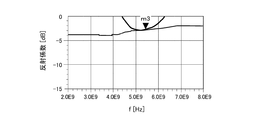
- FIG. 4 shows that at the main amplifier system end of the variable frequency amplifier when the phase shifter 10 and the attenuator 11 of the injection amplifier system 9 are set so that the output of the main amplifier system 4 becomes maximum at 5.4 GHz.
- FIG. 4 shows the calculation result of an output reflection characteristic.
- the curve in FIG. 4 is the calculation result of the reflection characteristic at the main amplifier system end of the variable frequency amplifier, and the substantially straight line rising to the right is the calculation result of the output reflection characteristic of the main amplifier system.
- FIG. 5 is an explanatory diagram showing the calculation result of the frequency dependence of the output power of the main amplifier system 4 excluding the power of the signal injected from the injection amplifier system 9. As can be seen from FIG. 5, the maximum output power is obtained in the vicinity of 5.4 GHz.
- FIG. 6 is an explanatory diagram showing calculation results of output reflection characteristics at the main amplifier system end of the frequency variable amplifier.
- the curve in FIG. 6 is the calculation result of the reflection characteristic at the main amplifier system end of the frequency variable amplifier, and the substantially straight line rising to the right is the calculation result of the output reflection characteristic of the main amplifier system.
- FIG. 6 it can be confirmed that the same reflection coefficient as that of the output side of the main amplifier system 4 is obtained at 4.5 GHz.
- FIG. 7 is an explanatory diagram showing the calculation result of the frequency dependence of the output power of the main amplifier system 4 excluding the power of the signal injected from the injection amplifier system 9. As is apparent from FIG. 7, it can be seen that the maximum output power is obtained in the vicinity of 4.5 GHz. From the above, it is confirmed by calculation that the frequency variable amplifier of FIG. 1 can be matched at an arbitrary frequency.
- the unit amplifiers 7a and 7b of the main amplifier system 4 are MMIC amplifiers that can obtain a saturated output power of about 20 dBm in a band of 6 GHz to 18 GHz and an output impedance of 50 ⁇ .
- the reflection coefficient on the output side of the MMIC amplifier is about ⁇ 3 dB in the vicinity of 6 GHz, and about ⁇ 20 dB in the vicinity of 18 GHz.
- FIG. 8 is an explanatory diagram showing the measurement result of the output power of the main amplifier system 4 excluding the power of the signal injected from the injection amplifier system 9. It can be confirmed that the output power in the vicinity of 6 GHz is greatly improved by injecting the output signal of the injection amplifier system 9 to the output side of the main amplifier system 4 and changing the output reflection coefficient of the main amplifier system 4. On the other hand, it can be confirmed that the output hardly changes in the vicinity of 18 GHz. This is probably because 6 GHz has poor output reflection characteristics of the main amplifier system 4 and is not matched, whereas 18 GHz has good output reflection characteristics and is matched. From the above, it is confirmed by calculation and measurement that the variable frequency amplifier of FIG. 1 can be matched at an arbitrary frequency.
- the main amplifier system 4 that amplifies one of the input signals distributed by the directional coupler 3 and outputs the amplified signal, is given from the outside. According to the set value, the amplitude and phase of the other input signal distributed by the directional coupler 3 are adjusted, the input signal is amplified, and the amplified signal is injected into the output side of the main amplifier system 4 Since the amplifier system 9 is provided, it is possible to achieve matching at an arbitrary frequency without causing an increase in loss.
- the reflection coefficient ⁇ viewed from the output side of the main amplifier system 4 is electrically changed, so that it is within the adjustable frequency band. Matching can be achieved at a single frequency. Therefore, there is an advantage that the number of matching frequencies is not limited. Further, unlike the conventional example, since no switch is used, there is an advantage that the matching circuit loss is small. Further, since the power of the signal injected from the injection amplifier system 9 to the main amplifier system 4 is reflected at the output terminal of the main amplifier system 4 and guided to the output terminal of the variable frequency amplifier, a loss occurs in the output matching circuit. Not have the advantage. In addition, since no switch is used, there are advantages that there is no problem of durability and that a frequency switching time is short.
- the injection amplifier system 9 is operated even at a frequency where the output reflection coefficient of the main amplifier system 4 is good, but only at a frequency where the output reflection characteristic of the main amplifier system 4 is bad.
- the injection amplifier system 9 may be operated.
- the injection amplifier system 9 may be operated according to the output power of the main amplifier system 4.
- the directional coupler 3 divides the input signal into two and supplies the signal to the main amplifier system 4 and the injection amplifier system 9, but the input supplied to the main amplifier system 4 is shown.
- the same signal as the input signal that is synchronized with the signal may be supplied to the injection amplifier system 9. That is, the same signal may be supplied to the main amplifier system 4 and the injection amplifier system 9 from different signal sources.
- phase shifter 10 and the attenuator 11 are provided on the input side of the injection amplifier 12. However, the phase shifter 10 and the attenuator 11 are on the output side of the injection amplifier 12. May be provided.
- the injection amplifier system 9 has both the phase shifter 10 and the attenuator 11. However, at least one of the phase shifter 10 and the attenuator 11 is mounted. Then, matching can be achieved at an arbitrary frequency without causing an increase in loss.
- Embodiment 2 FIG.
- the injection amplifier system 9 is mounted with the injection amplifier 12, but the injection amplifier system 9 is mounted with a variable gain amplifier instead of the attenuator 11 and the injection amplifier 12. You may do it.
- the configuration of the injection amplifier system 9 can be simplified.
- the injection amplifier system 9 includes the phase shifter 10 and the phase shifter 10 adjusts the phase of the input signal.
- a bias voltage is used as the injection amplifier 12 of the injection amplifier system 9. It is also possible to adjust the pass phase of the input signal by using an amplifier capable of controlling the above and controlling the bias voltage of the amplifier. This eliminates the need for the injection amplifier system 9 to mount the phase shifter 10, so that the configuration of the injection amplifier system 9 can be simplified.
- Embodiment 4 FIG.
- the directional coupler 3 distributes the input signal to the main amplifier system 4 and the injection amplifier system 9.
- the main amplifier system is distributed. 4 and the distribution ratio of the input signal to the injection amplifier system 9 may be adjusted.
- the injection amplifier system 9 is not equipped with the phase shifter 10 and the attenuator 11, matching can be achieved at an arbitrary frequency without increasing loss. Therefore, there is an effect that the configuration of the injection amplifier system 9 can be simplified.
- Embodiment 5 FIG.
- the directional coupler 3 distributes the input signal to the main amplifier system 4 and the injection amplifier system 9.
- the main amplifier system is distributed. 4 and the injection amplifier system 9 may be adjusted in phase.
- the injection amplifier system 9 is not equipped with the phase shifter 10 and the attenuator 11, matching can be achieved at an arbitrary frequency without increasing loss. Therefore, there is an effect that the configuration of the injection amplifier system 9 can be simplified.
- FIG. 9 is a block diagram showing a variable frequency amplifier according to Embodiment 6 of the present invention.
- the circulator 19 is connected to the output side of the main amplifier system 4, and the output side of the injection amplifier system 9 is connected to the isolation port of the circulator 19.
- variable frequency amplifier of FIG. 9 The basic operation of the variable frequency amplifier of FIG. 9 is the same as that of the variable frequency amplifier of FIG. 1, but as shown in FIG. 9, a circulator 19 is connected to the output side of the main amplifier system 4. If the output side of the injection amplifier system 9 is connected to the isolation port, the main amplifier system is not a balanced amplifier but only one unit amplifier 7a as in the main amplifier system 4 in the variable frequency amplifier of FIG. 4 can be configured.
- variable frequency amplifier can be configured even with an amplifier having a general configuration that does not have a balanced type.
- the circulator 19 is connected to the output side of the main amplifier system 4, the reflection characteristics of the main amplifier system 4 are hardly affected by the outside, and errors in the set values of the amplitude and phase in the injection amplifier system 9 are reduced. be able to.
- Embodiment 7 FIG.
- the main amplifier system 4 and the injection amplifier system 9 are not provided with a delay circuit.
- a delay circuit that matches the delay times of the main amplifier system 4 and the injection amplifier system 9 may be mounted on at least one of the main amplifier system 4 or the injection amplifier system 9.
- a delay circuit including a delay line and a delay filter may be mounted on at least one of the main amplifier system 4 or the injection amplifier system 9.
- Embodiment 8 FIG.
- the phase shifter 10 and the attenuator 11 of the injection amplifier system 9 are set so that the difference between the power displayed by the power meter 17 and the power displayed by the power meter 18 is maximized.
- the main amplifier system 4 is matched at an arbitrary frequency.
- a power meter (between the unit amplifier 7a (or the unit amplifier 7b) and the 3 dB directional coupler 8 is connected). If the power meter measures the power of the output signal of the unit amplifier 7a (or unit amplifier 7b) and displays the power, it is displayed by the power meter.
- the main frequency can be set at an arbitrary frequency. It may be matching the width unit system 4.
- a power meter (not shown) connected between the unit amplifier 7 a (or unit amplifier 7 b) and the 3 dB directional coupler 8, which is injected from the injection amplifier system 9. If the power of the signal is measured and displayed, the injection amplifier is such that the difference between the power displayed by the power meter and the power displayed by the power meter 17 is maximized.
- the main amplifier system 4 may be matched at an arbitrary frequency.
- a first power meter (not shown) connected between the unit amplifier 7a (or the unit amplifier 7b) and the 3 dB directional coupler 8, and the first power meter is connected to the unit amplifier 7a.
- the power of the output signal of (or the unit amplifier 7b) is measured and displayed, and the second power connected between the unit amplifier 7a (or the unit amplifier 7b) and the 3 dB directional coupler 8 is displayed.
- the first power meter (not shown) By setting the phase shifter 10 and the attenuator 11 of the injection amplifier system 9 so as to maximize the difference between the power displayed by the meter and the power displayed by the second power meter, any At the frequency of It may be matching the width unit system 4.
- variable frequency amplifier can achieve matching at an arbitrary frequency without causing an increase in loss, it is suitable for use in a power amplifier mounted on a software defined radio.
Landscapes
- Engineering & Computer Science (AREA)
- Power Engineering (AREA)
- Physics & Mathematics (AREA)
- Nonlinear Science (AREA)
- Amplifiers (AREA)
Abstract
Description
周波数や変調方式をはじめとして、無線通信方式が多様化しており、今日、数多くの無線通信方式が混在している。
複数の無線通信方式に対応するには、各周波数や変調方式毎にハードウェアが必要となるため、無線機が大型化する傾向にある。
そのため、ソフトウェアによって周波数や変調方式を変更することで、複数の無線通信方式に対応することが可能なソフトウエア無線機が望まれている。
ソフトウエア無線機では、各周波数や変調方式毎にハードウェアを用意する必要がないため、無線機の小型化を図ることができる。
このような電力増幅器を単一の増幅器で実現しようとする場合において、高効率特性・高出力特性・広帯域特性を得るための手法として、周波数毎に電力増幅器の整合回路を切り替える手法などが提案されている。
実施の形態1.
図1はこの発明の実施の形態1による周波数可変増幅器を示す構成図である。
図1において、入力端子1は増幅対象の信号を入力する端子である。
方向性結合器2は入力端子1から入力された信号(以下、「入力信号」と称する)を方向性結合器3とパワーメータ16に分配する分配器である。
方向性結合器3は方向性結合器2により分配された入力信号を主増幅器系4と注入増幅器系9に分配する分配器である。
なお、方向性結合器3は信号分配手段を構成している。
主増幅器系4のアイソレーション抵抗5は一端が接地され、他端が3dB方向性結合器6の入力側と接続されている抵抗である。
3dB方向性結合器6は入力側がアイソレーション抵抗5及び方向性結合器3と接続されており、方向性結合器3により分配された入力信号を単位増幅器7a,7bに分配する分配器である。
3dB方向性結合器8は入力側が単位増幅器7a,7bと接続され、かつ、出力側が方向性結合器13,15を介して出力端子14及び注入増幅器系9と接続されており、注入増幅器系9の出力信号の注入を受けながら、単位増幅器7a,7bによる増幅後の信号を出力端子14に出力する分配器である。
注入増幅器系9の移相器10は外部から与えられる設定値にしたがって入力信号の位相を調整する移相手段である。
減衰器11は外部から与えられる設定値にしたがって入力信号の振幅を調整する減衰手段である。
注入増幅器12は減衰器11による振幅調整後の信号を増幅して、増幅後の信号を注入増幅器系9の出力側に注入する。
出力端子14は方向性結合器13により分配された信号を出力する端子である。
方向性結合器15は注入増幅器系9の出力信号を主増幅器系4の出力側とパワーメータ18に分配する分配器である。
パワーメータ16は入力信号の電力を測定して、その入力信号の電力を表示する表示機器である。
パワーメータ17は主増幅器系4の出力信号の電力を測定して、その出力信号の電力を表示する第1の表示機器である。
パワーメータ18は注入増幅器系9の出力信号の電力を測定して、その出力信号の電力を表示する第2の表示機器である。
図2は図1の周波数可変増幅器の動作に関する模式図である。
方向性結合器2は、入力端子1から信号が入力されると、その入力信号を方向性結合器3とパワーメータ16に分配する。
方向性結合器3は、方向性結合器2から分配された入力信号を受けると、その入力信号を主増幅器系4と注入増幅器系9に分配する。
即ち、主増幅器系4の3dB方向性結合器6は、方向性結合器3から分配された入力信号を受けると、その入力信号を単位増幅器7a,7bに分配する。
主増幅器系4の単位増幅器7a,7bは、3dB方向性結合器6から分配された入力信号を受けると、その入力信号を増幅して、増幅後の信号を3dB方向性結合器8に出力する。
主増幅器系4の3dB方向性結合器8は、単位増幅器7a,7bから増幅後の信号を受けると、その増幅後の信号を出力端子14に出力する。
主増幅器系4の出力端において、注入増幅器系9の出力信号が注入されない場合の主増幅器系4の出力側から負荷側を見込んだ反射係数Γは、下記の式(1)のように定義される。

また、Viは主増幅器系4の出力側から負荷側に向かう信号の電圧振幅、θiは主増幅器系4の出力側から負荷側に向かう信号の位相を表している。
反射係数Γは、式(1)に示すように、負荷側から主増幅器系4の出力側に向かう信号と、主増幅器系4の出力側から負荷側に向かう信号との電圧振幅・位相比で表されるので、負荷側から主増幅器系4の出力側に向かう信号の電圧振幅及び位相が変われば、反射係数Γが変化することが分かる。
負荷側から主増幅器系4の出力側に向かう信号は、注入増幅器系9から注入される信号と、主増幅器系4の出力インピーダンスと負荷インピーダンスの不一致により発生した反射波の和で表されるので、主増幅器系4の出力信号注入時の反射係数Γは、下記の式(2)のように定義される。

主増幅器系4が整合されている状態では、注入増幅器系9から注入される信号の電力を除いた主増幅器系4の出力が最大となるので、主増幅器系4の出力が最大となるように、注入増幅器系9の移相器10及び減衰器11を設定すればよいことが分かる。
また、注入増幅器系9から主増幅器系4に注入される信号の電力は、パワーメータ18により測定されて表示される。
注入増幅器系9から注入される信号の電力を除いた主増幅器系4の出力は、パワーメータ17により表示されている電力と、パワーメータ18により表示されている電力との差で求めることができる。
以上より、パワーメータ17により表示されている電力と、パワーメータ18により表示されている電力との差が最大となるように、注入増幅器系9の移相器10及び減衰器11を設定すれば、任意の周波数で主増幅器系4の整合を取ることができることが分かる。
図3は主増幅器系4の入出力反射特性の計算結果を示す説明図である。図3中の曲線は入力反射特性の計算結果であり、右上がりの略直線は出力反射特性の計算結果である。
主増幅器系4の出力側の反射特性は、0GHz~8GHzにおいて、概ね“-3dB”が得られている。この増幅器を用いて周波数可変増幅器を構成する。
図4は、5.4GHzにおいて、主増幅器系4の出力が最大となるように、注入増幅器系9の移相器10及び減衰器11を設定した場合の周波数可変増幅器の主増幅器系端での出力反射特性の計算結果を示す説明図である。図4中の曲線は周波数可変増幅器の主増幅器系端での反射特性の計算結果であり、右上がりの略直線は主増幅器系の出力反射特性の計算結果である。
図4から明らかなように、5.4GHzにおいて、主増幅器系4の出力側の反射係数と同じ反射係数が得られていることが確認できる。
図5は注入増幅器系9から注入される信号の電力を除いた主増幅器系4の出力電力の周波数依存性の計算結果を示す説明図である。
図5から明らかなように、5.4GHz近傍において、最大出力電力が得られていることが分かる。
図6は周波数可変増幅器の主増幅器系端での出力反射特性の計算結果を示す説明図である。図6中の曲線は周波数可変増幅器の主増幅器系端での反射特性の計算結果であり、右上がりの略直線は主増幅器系の出力反射特性の計算結果である。
図6から明らかなように、4.5GHzにおいて、主増幅器系4の出力側の反射係数と同じ反射係数が得られていることが確認できる。
図7は注入増幅器系9から注入される信号の電力を除いた主増幅器系4の出力電力の周波数依存性の計算結果を示す説明図である。
図7から明らかなように、4.5GHz近傍において、最大出力電力が得られていることが分かる。
以上より、図1の周波数可変増幅器が任意の周波数で整合が取れることが、計算上で確認される。
主増幅器系4の単位増幅器7a,7bには、帯域6GHz~18GHz、出力インピーダンス50Ωにおいて、約20dBmの飽和出力電力が得られるMMIC増幅器を用いている。
MMIC増幅器の出力側の反射係数は、6GHz近傍で、-3dB程度であり、18GHz近傍では、-20dB程度である。
図8は注入増幅器系9から注入される信号の電力を除いた主増幅器系4の出力電力の測定結果を示す説明図である。
注入増幅器系9の出力信号を主増幅器系4の出力側に注入し、主増幅器系4の出力反射係数を変化させることで、6GHz近傍での出力電力が大きく改善されていることが確認できる。
一方、18GHz近傍では、ほとんど出力が変化していないことが確認できる。
これは、6GHzは、主増幅器系4の出力反射特性が悪く、整合が取れていない一方、18GHzでは、出力反射特性が良好で整合が取れているためであると考えられる。
以上より、図1の周波数可変増幅器が任意の周波数で整合が取れることが、計算・実測上で確認される。
また、従来例のように、スイッチを使用しないため、整合回路損失が小さい利点を有する。
さらに、注入増幅器系9から主増幅器系4に注入する信号の電力は、主増幅器系4の出力端で反射されて、周波数可変増幅器の出力端に導かれるため、出力整合回路での損失が発生しない利点を有する。
この他にも、スイッチを使用しないため、耐久性の問題がない利点や、周波数の切り替え時間が短いなどの利点がある。
即ち、別々の信号源から同一の信号を主増幅器系4及び注入増幅器系9に供給するようにしてもよい。
上記実施の形態1では、注入増幅器系9が注入増幅器12を実装しているものについて示したが、注入増幅器系9が減衰器11及び注入増幅器12の代わりに、利得可変増幅器を実装しているようにしてもよい。
これにより、注入増幅器系9の構成を簡略化することができる効果を奏する。
上記実施の形態1では、注入増幅器系9が移相器10を実装し、移相器10が入力信号の位相を調整するものについて示したが、注入増幅器系9の注入増幅器12として、バイアス電圧の制御が可能な増幅器を使用し、その増幅器のバイアス電圧を制御することで、入力信号の通過位相を調整するようにしてもよい。
これにより、注入増幅器系9が移相器10を実装する必要がなくなるため、注入増幅器系9の構成を簡略化することができる効果を奏する。
上記実施の形態1では、方向性結合器3が入力信号を主増幅器系4及び注入増幅器系9に分配するものについて示したが、方向性結合器3が入力信号を分配する際、主増幅器系4及び注入増幅器系9に対する入力信号の分配比を調整するようにしてもよい。
この場合、注入増幅器系9が移相器10及び減衰器11を実装していなくても、損失の増加を招くことなく、任意の周波数で整合を取ることができる。
そのため、注入増幅器系9の構成を簡略化することができる効果を奏する。
上記実施の形態1では、方向性結合器3が入力信号を主増幅器系4及び注入増幅器系9に分配するものについて示したが、方向性結合器3が入力信号を分配する際、主増幅器系4及び注入増幅器系9に分配する入力信号の位相を調整するようにしてもよい。
この場合、注入増幅器系9が移相器10及び減衰器11を実装していなくても、損失の増加を招くことなく、任意の周波数で整合を取ることができる。
そのため、注入増幅器系9の構成を簡略化することができる効果を奏する。
図9はこの発明の実施の形態6による周波数可変増幅器を示す構成図であり、図において、図1と同一符号は同一又は相当部分を示すので説明を省略する。
サーキュレータ19は主増幅器系4の出力側に接続されており、サーキュレータ19のアイソレーションポートには、注入増幅器系9の出力側が接続されている。
また、主増幅器系4の出力側にサーキュレータ19が接続されるため、主増幅器系4の反射特性が外部の影響を受け難くなり、注入増幅器系9における振幅や位相の設定値の誤差を小さくすることができる。
上記実施の形態1では、主増幅器系4及び注入増幅器系9に遅延回路が実装されていないものを示したが、主増幅器系4及び注入増幅器系9の遅延時間を一致させる遅延回路(例えば、遅延線路や遅延フィルタなどから構成される遅延回路)を、主増幅器系4又は注入増幅器系9の少なくとも一方に実装するようにしてもよい。
このように、主増幅器系4及び注入増幅器系9の遅延時間を一致させることで、周波数可変増幅器の広帯域化を図ることができる効果を奏する。
上記実施の形態1では、パワーメータ17により表示されている電力と、パワーメータ18により表示されている電力との差が最大となるように、注入増幅器系9の移相器10及び減衰器11を設定することで、任意の周波数で主増幅器系4の整合を取るものについて示したが、単位増幅器7a(または単位増幅器7b)と3dB方向性結合器8の間に接続されているパワーメータ(図示せず)であって、そのパワーメータが、単位増幅器7a(または単位増幅器7b)の出力信号の電力を測定して、その電力を表示するものであれば、そのパワーメータにより表示されている電力と、パワーメータ18により表示されている電力との差が最大となるように、注入増幅器系9の移相器10及び減衰器11を設定することで、任意の周波数で主増幅器系4の整合を取るようにしてもよい。
Claims (15)
- 入力信号を分配する信号分配手段と、上記信号分配手段により分配された一方の入力信号を増幅して増幅後の信号を出力する主増幅手段と、外部から与えられる設定値にしたがって、上記信号分配手段により分配された他方の入力信号の振幅又は位相の少なくとも一方を調整するとともに、上記入力信号を増幅して増幅後の信号を上記主増幅手段の出力側に注入する注入増幅手段とを備えた周波数可変増幅器。
- 入力信号を増幅して増幅後の信号を出力する主増幅手段と、外部から与えられる設定値にしたがって、上記入力信号と同期が取られている上記入力信号と同一の信号を入力して、上記同一の信号である入力信号の振幅又は位相の少なくとも一方を調整するとともに、上記入力信号を増幅して増幅後の信号を上記主増幅手段の出力側に注入する注入増幅手段とを備えた周波数可変増幅器。
- 主増幅手段は、出力側のアイソレーションポートから注入増幅手段の出力信号が注入されるバランス型増幅器を用いて構成されていることを特徴とする請求項1記載の周波数可変増幅器。
- 主増幅手段は、出力側のアイソレーションポートから注入増幅手段の出力信号が注入されるバランス型増幅器を用いて構成されていることを特徴とする請求項2記載の周波数可変増幅器。
- 注入増幅手段は、外部から与えられる設定値にしたがって入力信号の振幅を調整する減衰器、または、外部から与えられる設定値にしたがって上記入力信号の位相を調整する移相器の少なくとも一方が実装されていることを特徴とする請求項1記載の周波数可変増幅器。
- 注入増幅手段は、外部から与えられる設定値にしたがって入力信号の振幅を調整する減衰器、または、外部から与えられる設定値にしたがって上記入力信号の位相を調整する移相器の少なくとも一方が実装されていることを特徴とする請求項2記載の周波数可変増幅器。
- 注入増幅手段は、入力信号の利得の調整が可能な利得可変増幅器、または、バイアス電圧が制御されることで上記入力信号の通過位相が調整可能な増幅器を用いて構成されていることを特徴とする請求項1記載の周波数可変増幅器。
- 注入増幅手段は、入力信号の利得の調整が可能な利得可変増幅器、または、バイアス電圧が制御されることで上記入力信号の通過位相が調整可能な増幅器を用いて構成されていることを特徴とする請求項2記載の周波数可変増幅器。
- 信号分配手段は、主増幅手段及び注入増幅手段に対する入力信号の分配比、または、主増幅手段及び注入増幅手段に分配する入力信号の位相を調整することを特徴とする請求項1記載の周波数可変増幅器。
- 主増幅手段の出力側にサーキュレータが接続されており、注入増幅手段の出力側が上記サーキュレータのアイソレーションポートと接続されていることを特徴とする請求項1記載の周波数可変増幅器。
- 主増幅手段の出力側にサーキュレータが接続されており、注入増幅手段の出力側が上記サーキュレータのアイソレーションポートと接続されていることを特徴とする請求項2記載の周波数可変増幅器。
- 主増幅手段と注入増幅手段の遅延時間を一致させる遅延回路が、上記主増幅手段又は上記注入増幅手段の少なくとも一方に実装されていることを特徴とする請求項1記載の周波数可変増幅器。
- 主増幅手段と注入増幅手段の遅延時間を一致させる遅延回路が、上記主増幅手段又は上記注入増幅手段の少なくとも一方に実装されていることを特徴とする請求項2記載の周波数可変増幅器。
- 主増幅手段の出力信号の電力を測定して、上記電力を表示する第1の表示機器と、注入増幅手段から上記主増幅手段の出力側に注入される信号の電力を測定して、上記電力を表示する第2の表示機器とを設けたことを特徴とする請求項1記載の周波数可変増幅器。
- 主増幅手段の出力信号の電力を測定して、上記電力を表示する第1の表示機器と、注入増幅手段から上記主増幅手段の出力側に注入される信号の電力を測定して、上記電力を表示する第2の表示機器とを設けたことを特徴とする請求項2記載の周波数可変増幅器。
Priority Applications (2)
| Application Number | Priority Date | Filing Date | Title |
|---|---|---|---|
| US13/058,008 US8416018B2 (en) | 2008-11-10 | 2009-11-04 | Variable frequency amplifier |
| JP2010536686A JP5111614B2 (ja) | 2008-11-10 | 2009-11-04 | 周波数可変増幅器 |
Applications Claiming Priority (2)
| Application Number | Priority Date | Filing Date | Title |
|---|---|---|---|
| JP2008-287879 | 2008-11-10 | ||
| JP2008287879 | 2008-11-10 |
Publications (1)
| Publication Number | Publication Date |
|---|---|
| WO2010052901A1 true WO2010052901A1 (ja) | 2010-05-14 |
Family
ID=42152714
Family Applications (1)
| Application Number | Title | Priority Date | Filing Date |
|---|---|---|---|
| PCT/JP2009/005850 Ceased WO2010052901A1 (ja) | 2008-11-10 | 2009-11-04 | 周波数可変増幅器 |
Country Status (3)
| Country | Link |
|---|---|
| US (1) | US8416018B2 (ja) |
| JP (1) | JP5111614B2 (ja) |
| WO (1) | WO2010052901A1 (ja) |
Cited By (1)
| Publication number | Priority date | Publication date | Assignee | Title |
|---|---|---|---|---|
| KR101712753B1 (ko) * | 2015-12-31 | 2017-03-08 | 서울시립대학교 산학협력단 | 높은 이득 특성을 갖는 피드백 포트 증폭기 및 그 동작방법 |
Families Citing this family (6)
| Publication number | Priority date | Publication date | Assignee | Title |
|---|---|---|---|---|
| US9166536B2 (en) | 2012-10-30 | 2015-10-20 | Eta Devices, Inc. | Transmitter architecture and related methods |
| US9537456B2 (en) | 2012-10-30 | 2017-01-03 | Eta Devices, Inc. | Asymmetric multilevel backoff amplifier with radio-frequency splitter |
| US8829993B2 (en) | 2012-10-30 | 2014-09-09 | Eta Devices, Inc. | Linearization circuits and methods for multilevel power amplifier systems |
| US9768731B2 (en) | 2014-07-23 | 2017-09-19 | Eta Devices, Inc. | Linearity and noise improvement for multilevel power amplifier systems using multi-pulse drain transitions |
| GB201423350D0 (en) * | 2014-12-30 | 2015-02-11 | Selex Es Ltd | A radio frequency power amplifier |
| US9979421B2 (en) | 2015-03-02 | 2018-05-22 | Eta Devices, Inc. | Digital pre-distortion (DPD) training and calibration system and related techniques |
Citations (6)
| Publication number | Priority date | Publication date | Assignee | Title |
|---|---|---|---|---|
| JPS5251875A (en) * | 1975-10-23 | 1977-04-26 | Nec Corp | Method and apparatus for measuring characteristics of super high frequ ency transistors |
| JPH06347495A (ja) * | 1993-06-08 | 1994-12-22 | Nippon Hoso Kyokai <Nhk> | ハイビジョン用伝送特性測定器 |
| JPH088660A (ja) * | 1994-06-24 | 1996-01-12 | Nec Corp | 電力合成用位相制御回路 |
| JP2002076781A (ja) * | 2000-09-05 | 2002-03-15 | Mitsubishi Electric Corp | 高周波増幅器、フィードフォワード増幅器および歪み補償増幅器 |
| JP2004301562A (ja) * | 2003-03-28 | 2004-10-28 | Nec Corp | アクティブロードプル測定法及びアクティブロードプル測定回路 |
| JP2006166141A (ja) * | 2004-12-08 | 2006-06-22 | Matsushita Electric Ind Co Ltd | ドハティ増幅器 |
Family Cites Families (7)
| Publication number | Priority date | Publication date | Assignee | Title |
|---|---|---|---|---|
| FR2466155A1 (fr) * | 1979-09-19 | 1981-03-27 | Lgt Lab Gen Telecomm | Dispositif d'amplification de puissance de signaux modules en amplitude, a haute performance, et emetteur et reemetteur de television comportant un tel dispositif |
| US6006111A (en) * | 1997-10-08 | 1999-12-21 | Nortel Networks Corporation | Self-balancing matrix amplifier |
| KR200212866Y1 (ko) * | 1998-12-26 | 2001-02-15 | 서평원 | 선왜곡 방식 전력증폭기용 능동 왜곡신호 발생회로 |
| US6799020B1 (en) * | 1999-07-20 | 2004-09-28 | Qualcomm Incorporated | Parallel amplifier architecture using digital phase control techniques |
| US6825719B1 (en) * | 2000-05-26 | 2004-11-30 | Intel Corporation | RF power amplifier and methods for improving the efficiency thereof |
| US7183843B1 (en) * | 2005-06-27 | 2007-02-27 | Rockwell Collins, Inc. | Electronically tuned power amplifier |
| GB0822659D0 (en) * | 2008-12-12 | 2009-01-21 | Astrium Ltd | Multiport amplifier adjustment |
-
2009
- 2009-11-04 WO PCT/JP2009/005850 patent/WO2010052901A1/ja not_active Ceased
- 2009-11-04 JP JP2010536686A patent/JP5111614B2/ja not_active Expired - Fee Related
- 2009-11-04 US US13/058,008 patent/US8416018B2/en not_active Expired - Fee Related
Patent Citations (6)
| Publication number | Priority date | Publication date | Assignee | Title |
|---|---|---|---|---|
| JPS5251875A (en) * | 1975-10-23 | 1977-04-26 | Nec Corp | Method and apparatus for measuring characteristics of super high frequ ency transistors |
| JPH06347495A (ja) * | 1993-06-08 | 1994-12-22 | Nippon Hoso Kyokai <Nhk> | ハイビジョン用伝送特性測定器 |
| JPH088660A (ja) * | 1994-06-24 | 1996-01-12 | Nec Corp | 電力合成用位相制御回路 |
| JP2002076781A (ja) * | 2000-09-05 | 2002-03-15 | Mitsubishi Electric Corp | 高周波増幅器、フィードフォワード増幅器および歪み補償増幅器 |
| JP2004301562A (ja) * | 2003-03-28 | 2004-10-28 | Nec Corp | アクティブロードプル測定法及びアクティブロードプル測定回路 |
| JP2006166141A (ja) * | 2004-12-08 | 2006-06-22 | Matsushita Electric Ind Co Ltd | ドハティ増幅器 |
Cited By (1)
| Publication number | Priority date | Publication date | Assignee | Title |
|---|---|---|---|---|
| KR101712753B1 (ko) * | 2015-12-31 | 2017-03-08 | 서울시립대학교 산학협력단 | 높은 이득 특성을 갖는 피드백 포트 증폭기 및 그 동작방법 |
Also Published As
| Publication number | Publication date |
|---|---|
| JPWO2010052901A1 (ja) | 2012-04-05 |
| JP5111614B2 (ja) | 2013-01-09 |
| US8416018B2 (en) | 2013-04-09 |
| US20110140776A1 (en) | 2011-06-16 |
Similar Documents
| Publication | Publication Date | Title |
|---|---|---|
| JP5111614B2 (ja) | 周波数可変増幅器 | |
| Gustafsson et al. | A modified Doherty power amplifier with extended bandwidth and reconfigurable efficiency | |
| US9667198B2 (en) | Power amplifier | |
| JP2004173231A (ja) | ドハティ増幅器を用いた信号増幅装置 | |
| CN102696172B (zh) | 具有多合体扩展的高频功率放大器 | |
| CA2616285A1 (en) | Predistortion linearization device with adjustable amplitude and shape | |
| CN106257827B (zh) | 对称多赫蒂Doherty功放电路装置及功率放大器 | |
| AU2008202176B2 (en) | Delay modulator pre-distortion circuit for an amplifier | |
| TW558865B (en) | A radio frequency amplifying circuit | |
| US7183843B1 (en) | Electronically tuned power amplifier | |
| CN109951166A (zh) | 一种微波功率放大方法及装置 | |
| JPH07101820B2 (ja) | 低歪高周波増幅装置 | |
| JP2008236105A (ja) | 電力分配合成システム | |
| JP2012065082A (ja) | ドハティ増幅器 | |
| JP4211128B2 (ja) | 多チャネル高周波信号供給装置 | |
| EP2621084A1 (en) | Power amplifier with modified doherty topology | |
| Sah et al. | Prototype for an optimized drive signal control system for a 2.5 GHz Doherty power amplifier | |
| US6977554B2 (en) | Variable gain amplifier for high frequency band using microstrip hybrid | |
| JP2003332852A (ja) | プリディストーション回路 | |
| JP2012205018A (ja) | 高出力電力増幅器 | |
| JP2018074255A (ja) | ドハティ型増幅器 | |
| CN113114124A (zh) | 一种空间行波管宽频带可调线性化器 | |
| JP6645333B2 (ja) | ドハティ増幅器 | |
| JP5606371B2 (ja) | ドハティ増幅器 | |
| GB2437573A (en) | Combiner circuit for Doherty amplifier |
Legal Events
| Date | Code | Title | Description |
|---|---|---|---|
| 121 | Ep: the epo has been informed by wipo that ep was designated in this application |
Ref document number: 09824601 Country of ref document: EP Kind code of ref document: A1 |
|
| WWE | Wipo information: entry into national phase |
Ref document number: 2010536686 Country of ref document: JP |
|
| WWE | Wipo information: entry into national phase |
Ref document number: 13058008 Country of ref document: US |
|
| NENP | Non-entry into the national phase |
Ref country code: DE |
|
| 122 | Ep: pct application non-entry in european phase |
Ref document number: 09824601 Country of ref document: EP Kind code of ref document: A1 |