WO2010058950A2 - 태양 전지용 전극의 제조방법, 이를 이용하여 제조된 태양 전지용 기판 및 태양 전지 - Google Patents
태양 전지용 전극의 제조방법, 이를 이용하여 제조된 태양 전지용 기판 및 태양 전지 Download PDFInfo
- Publication number
- WO2010058950A2 WO2010058950A2 PCT/KR2009/006783 KR2009006783W WO2010058950A2 WO 2010058950 A2 WO2010058950 A2 WO 2010058950A2 KR 2009006783 W KR2009006783 W KR 2009006783W WO 2010058950 A2 WO2010058950 A2 WO 2010058950A2
- Authority
- WO
- WIPO (PCT)
- Prior art keywords
- electrode
- solar cell
- plating
- substrate
- printing
- Prior art date
- Legal status (The legal status is an assumption and is not a legal conclusion. Google has not performed a legal analysis and makes no representation as to the accuracy of the status listed.)
- Ceased
Links
Images



Classifications
-
- H—ELECTRICITY
- H10—SEMICONDUCTOR DEVICES; ELECTRIC SOLID-STATE DEVICES NOT OTHERWISE PROVIDED FOR
- H10F—INORGANIC SEMICONDUCTOR DEVICES SENSITIVE TO INFRARED RADIATION, LIGHT, ELECTROMAGNETIC RADIATION OF SHORTER WAVELENGTH OR CORPUSCULAR RADIATION
- H10F10/00—Individual photovoltaic cells, e.g. solar cells
-
- H—ELECTRICITY
- H10—SEMICONDUCTOR DEVICES; ELECTRIC SOLID-STATE DEVICES NOT OTHERWISE PROVIDED FOR
- H10F—INORGANIC SEMICONDUCTOR DEVICES SENSITIVE TO INFRARED RADIATION, LIGHT, ELECTROMAGNETIC RADIATION OF SHORTER WAVELENGTH OR CORPUSCULAR RADIATION
- H10F77/00—Constructional details of devices covered by this subclass
- H10F77/20—Electrodes
- H10F77/206—Electrodes for devices having potential barriers
- H10F77/211—Electrodes for devices having potential barriers for photovoltaic cells
-
- H—ELECTRICITY
- H10—SEMICONDUCTOR DEVICES; ELECTRIC SOLID-STATE DEVICES NOT OTHERWISE PROVIDED FOR
- H10F—INORGANIC SEMICONDUCTOR DEVICES SENSITIVE TO INFRARED RADIATION, LIGHT, ELECTROMAGNETIC RADIATION OF SHORTER WAVELENGTH OR CORPUSCULAR RADIATION
- H10F71/00—Manufacture or treatment of devices covered by this subclass
-
- H—ELECTRICITY
- H10—SEMICONDUCTOR DEVICES; ELECTRIC SOLID-STATE DEVICES NOT OTHERWISE PROVIDED FOR
- H10F—INORGANIC SEMICONDUCTOR DEVICES SENSITIVE TO INFRARED RADIATION, LIGHT, ELECTROMAGNETIC RADIATION OF SHORTER WAVELENGTH OR CORPUSCULAR RADIATION
- H10F77/00—Constructional details of devices covered by this subclass
- H10F77/20—Electrodes
-
- Y—GENERAL TAGGING OF NEW TECHNOLOGICAL DEVELOPMENTS; GENERAL TAGGING OF CROSS-SECTIONAL TECHNOLOGIES SPANNING OVER SEVERAL SECTIONS OF THE IPC; TECHNICAL SUBJECTS COVERED BY FORMER USPC CROSS-REFERENCE ART COLLECTIONS [XRACs] AND DIGESTS
- Y02—TECHNOLOGIES OR APPLICATIONS FOR MITIGATION OR ADAPTATION AGAINST CLIMATE CHANGE
- Y02E—REDUCTION OF GREENHOUSE GAS [GHG] EMISSIONS, RELATED TO ENERGY GENERATION, TRANSMISSION OR DISTRIBUTION
- Y02E10/00—Energy generation through renewable energy sources
- Y02E10/50—Photovoltaic [PV] energy
Definitions
- the present invention relates to a method for manufacturing an electrode for a solar cell, a substrate for a solar cell and a solar cell manufactured using the same.
- a solar cell is a semiconductor device that converts solar energy into electrical energy and has a p-n junction.
- the basic structure is the same as that of a diode.
- the incident light is absorbed by the solar cell to cause interaction with materials constituting the semiconductor of the solar cell.
- electrons and holes which are minority carriers, are formed, and they move to both of the electrodes to which they are connected to obtain an electromotive force.
- crystalline silicon solar cells can be roughly divided into single crystal and polycrystalline forms.
- the monocrystalline material is high in purity and low in crystal defect density and thus has high efficiency, but is relatively expensive, and the polycrystalline material is generally used because it is relatively inexpensive but relatively inexpensive.
- the method for manufacturing a polycrystalline silicon solar cell is a substrate surface by etching suitable for a p-type polycrystalline silicon substrate having a constant size (for example, 5 "or 6") and a thickness (for example, 150 to 250 ⁇ m). After giving irregularities to the surface while eliminating the defects, the surface of the p-type substrate with a constant thickness (0.1 to 0.5 ⁇ m) by thermal diffusion method by supplying a substance containing phosphorus (P) or POCl3 in the gas phase or liquid phase Doping to form an n-type emitter of 40 to 100 ⁇ / ⁇ .
- P phosphorus
- a wet etching process using an acid or a base is included to remove by-products such as phosphorus-containing glass generated in this process, and to remove the doped P in the remaining portions except the front portion to which light is irradiated.
- a dry etching process using plasma is included.
- a process of cutting the edge surface using a laser may be included.
- crystalline or amorphous silicon nitride, silicon oxide, titanium oxide, or a combination thereof is deposited to an appropriate thickness (about 70 to 90 kPa for silicon nitride) in consideration of the refractive index of the material deposited by physical vacuum deposition.
- a P-type semiconductor layer electrode and an N-type semiconductor layer electrode are formed.
- the inventors considered forming an electrode pattern with a photoresist on the surface of a semiconductor wafer to form a metal deposition layer through a deposition process.
- the method using the photoresist has to remove the portion where the metal deposition layer is formed on the portion other than the base electrode after the deposition process, and also has to remove the photoresist layer, and the underlying metal electrode layer uses the deposition method.
- the adhesion with the semiconductor wafer is weak.
- electroless nickel-phosphorus plating containing n-dopant phosphorus (Phosphorus, P) is performed on a P-type silicon layer on a single crystal silicon wafer, and boron (p-type dopant) is formed on an N-type silicon layer.
- the plating film is formed by using a plating solution containing an actual dopant, it is an electrode including the dopant as a whole as well as the part of the contact, so that the wire resistance itself is actually a wire using silver used for an existing printing method electrode.
- the series resistance portion of the entire cell becomes larger due to deterioration than resistance.
- a photolithography process must be further performed before plating to form an electrode pattern for plating.
- Electrodes for solar cells mainly use screen printing to obtain relatively wide line widths ( A method of printing an electrode of 100 ⁇ m or more) is proposed.
- the screen printing method has a disadvantage in that a fine line width cannot be obtained.
- the inkjet printing method is not applicable to the solar cell electrode production method until now, that is, there is no industrial applicability so far.
- the development of a conductive ink that satisfies the characteristics as a solar cell electrode and satisfies physical properties such as viscosity suitable for the inkjet printing method must be preceded.
- Such a conductive ink for solar cell electrodes has not been developed yet.
- the present invention is to solve the above problems, it is possible to form an electrode with a fine line width using an offset printing process with high productivity, and to significantly compensate for the disadvantages of the offset printing method to produce an electrode having excellent electrical characteristics. It is an object of the present invention to provide a method for producing a solar cell electrode, a solar cell substrate and a solar cell manufactured using the same.
- a solar cell substrate comprising a plurality of busbar electrodes and finger electrodes formed on a front surface of a substrate, wherein the busbar electrodes and finger electrodes are formed by being plated after being offset printed using a conductive paste. to provide.
- any conventional configuration of the solar cell substrate may be employed and added as long as it is feasible and is not limited thereto and is included in the present invention.
- the bus bar electrode and the finger electrode may be formed in contact with each other perpendicularly.
- a rear electrode may be provided on the rear surface of the substrate.
- the kind of substrate is not limited, and any kind of substrate that can be used as a substrate for a solar cell is included.
- bus bar electrode is characterized in that the offset printing in the mesh shape in which the micro-pores are present, if necessary, the finger electrode may also be manufactured in a mesh form like the bus bar electrode.
- the offset printing is preferably performed only once, and the busbar electrode and the finger electrode may be printed simultaneously. It is better to carry out the plating after firing after the offset printing. It is also preferable to heat-treat the plated metal after the plating.
- the solar cell substrate of the present invention can be produced in the aspect ratio (height / line width) of the finger electrode in the range of 0.2 to 0.6, and the line width of the finger electrode is in the range of 30 ⁇ m to 100 ⁇ m, and the height is 5 ⁇ m to 20 It is characterized by being in the micrometer range.
- the present invention also provides a solar cell manufactured using the solar cell substrate, which has twice the efficiency as compared with a solar cell using a solar cell substrate manufactured by forming an electrode without plating after the offset printing.
- the solar cell characterized by the above is provided.
- the present invention also provides a solar cell manufactured using the solar cell substrate.
- the present invention also provides a method for manufacturing a solar cell electrode for producing a busbar electrode and a finger electrode on a substrate, comprising: a paste electrode printing step of printing a conductive paste on an substrate by an offset method; An electrode plating step of immersing in a wet plating solution after the electrode printing step to deposit an additional metal in the fine pores of the paste electrode; And a heat treatment step of forming an ohmic contact by heat treatment after the electrode plating step.
- the present invention also provides a method for manufacturing an electrode for a solar cell, which further comprises the step of firing the electrode after the paste electrode printing step.
- the bus bar electrode provides a method for manufacturing an electrode for a solar cell, characterized in that the offset printing once in a mesh shape in which fine pores exist.
- the present invention also provides a solar cell provided with a solar cell electrode manufactured using the method for producing a solar cell electrode, wherein the cell efficiency (Eff) is 10% or more, the fill factor (FF) is 50% or more, and the series Provided is a solar cell, which has a resistance (Rser) of 0.02 mA or less.
- the method for forming an electrode for a solar cell according to the present invention is simple, highly productive, and prints the electrode through an offset printing process capable of providing fine line width, and preferably, the busbar electrode is printed in a mesh form, and an additional metal layer is wetted. It is plated by metal plating method and filled with the plating metal in the area where metal is not filled, thereby reducing the sheet resistance of the busbar electrode, and the finger electrode line width can be realized within 100 microns by the combination of offset printing process and wet metal plating process.
- the aspect ratio of the electrode may be implemented to 0.2 to 0.6 to reduce the shielding rate of light, and to improve the efficiency of the solar cell by forming additional ohmic contacts between the plating metal and the silicon wafer layer through heat treatment after plating.
- 1 to 3 is a schematic perspective view and a cross-sectional view of a solar cell substrate including a plurality of bus bar electrodes formed on the front surface of the substrate and a finger electrode connected thereto according to an embodiment of the present invention in a manufacturing procedure,
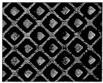
- 4 and 5 are schematic diagrams of bus bar electrode shapes and offset printing of mesh shapes in which fine voids exist in offset printing according to an embodiment of the present invention
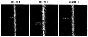
- FIG. 7 is an optical photograph ( ⁇ 100) of finger electrode line widths obtained in the manners of Example 1, Example 2 and Comparative Example 1.
- FIG. 7 is an optical photograph ( ⁇ 100) of finger electrode line widths obtained in the manners of Example 1, Example 2 and Comparative Example 1.
- the present inventors are required to reduce the line width of the finger electrode connected to the busbar and to increase the aspect ratio of the finger electrode in order to minimize the shielding of sunlight and to increase the efficiency.
- the solar cell electrode pattern is formed by offset printing. The method of study was studied. However, in the case of offset printing by conventional methods, a desired fine line width can be obtained in the case of a finger electrode requiring a fine line width of less than 100 ⁇ m, but in the case of printing a wide line width such as a busbar electrode, the set process This was not done smoothly.
- the set process is smoothly performed and at the same time, a desired finger is provided. It was found that the fine line width of the electrode can also be realized.
- the printability was improved when applied in the form of a mesh in order to improve the blister shock problem.
- the conductive paste layer is laminated in a mesh shape, the electrode thickness is uneven to increase the sheet resistance and the line resistance value, and after firing, the ohmic contact area range between the silicon wafer layer and the conductive paste layer decreases and thus the solar cell There is a problem of reducing the efficiency.
- the offset printing in order to increase the aspect ratio of the electrode and increase the efficiency of the solar cell, the offset printing must be implemented in at least two or more multilayers, so that the production cost is drastically increased. There is a rising problem. In addition, even if printed two or more times, there remains a problem that the wire resistance of the electrode is not significantly improved due to the intermetallic voids in the front electrode metal layer.
- the present invention forms a conductive front electrode having a narrow line width on the substrate by an offset printing process and fills the pores between metal particles in the metal electrode forming the electrode by plating the substrate by dipping the substrate in a wet plating solution.
- FIG. 1 to 3 are schematic perspective views and cross-sectional views of a solar cell substrate including a plurality of busbar electrodes and finger electrodes formed on a front surface of a substrate according to an embodiment of the present invention in a manufacturing procedure.
- the substrate 1 is offset printed using a conductive paste to form a busbar electrode 2 and a finger electrode 3 as paste electrodes (FIG. 2), and then the plating layer 4 is formed by plating. It is characterized by the formation (Fig. 3).
- the busbar electrode 2 and the finger electrode 3 as the paste electrode may undergo a firing process before plating, and the plating layer 4 may be heat treated after plating.
- the electrode formed on the substrate may be manufactured by the following example method. That is, in the method of manufacturing a solar cell electrode for manufacturing a busbar electrode and a finger electrode on a substrate, a paste electrode printing step of printing the busbar electrode and the finger electrode by an offset method using a conductive paste on the substrate And an electrode plating step of immersing the additional metal in the microcavity of the paste electrode by immersing in a wet plating solution after the electrode printing step, and a heat treatment step of heat-treating after the electrode plating step to form an ohmic contact. It may be prepared according to the manufacturing method.
- the paste electrode firing step may be further roughened between the paste electrode printing step and the plating step.
- the conductive paste used for the electrode printing may use materials known in the art and is not limited.
- the paste which consists of silver, copper, nickel, aluminum, etc. as a main component is used a lot, but the silver paste containing silver powder is mainly used.
- a silver paste composed of 60 to 85 wt% silver powder, 3 to 20 wt% glass powder, 2 to 10 wt% polymer binder, 3 to 20 wt% diluent solvent, and 0.1 to 5 wt% additives Is preferable because it is suitable for offset printing.
- the conductive paste may be printed by screen printing, offset printing, inkjet printing, or the like.
- the printing thickness is limited to less than 5 microns, and the thickness of the conductive paste is limited. Since a low viscosity type material having a viscosity of 50 cPs or less is suitable, it is not suitable for printing a high viscosity type conductive paste containing 60% or more of metal powder.
- the screen printing method is mainly used, but the line width of the formed electrode is relatively wide (more than 100 microns), which is the front electrode for solar cells, which increases the rate of shielding the front electrode (shielding rate or shading loss) when irradiated with light. There is a problem that the battery cell efficiency is reduced.
- the present invention is characterized in that the offset printing method is applied to the solar cell front electrode manufacturing method different from the screen printing and inkjet printing.
- a mesh pattern bus bar electrode pattern optimized for offset printing aptitude to prevent a blade from splashing on the bus bar during printing.
- the mesh shape defined in the present invention corresponds to any pattern in which micro voids exist, and the shape of the mesh may be various, including a rectangle, a triangle, a hexagon, a circle, a random shape, or a dot shape.
- the solar cell electrode pattern may be printed only once by an offset method using a conductive paste (the present invention is not limited to a single print), and the busbar electrode and the finger electrode may be printed simultaneously. It is also possible. When printing once, the process is simple because the number of printing is small, and there is an advantage that the amount of expensive conductive paste used is small. However, due to the area where the conductive paste is not filled in the mesh-shaped busbar pattern as shown in FIG. 6, the surface resistance and the line resistance of the busbar pattern are increased, and ohmic contact with the silicon wafer layer is not completely made after firing. There may be a problem that the battery cell efficiency is reduced, but the present invention provides a special means for solving this problem to obtain an electrode of excellent performance, which will be described later.
- the step of firing the electrode after the paste electrode printing step may be added.
- the electrical properties can be improved by firing the composition of the paste to remove insulating materials such as polymer binders and solvents.
- the firing conditions are not limited but it is preferable to bake for several seconds to several hours at a temperature of 600 to 900 °C.
- an additional metal plating layer is formed on the conductive paste electrode by the plating process.
- An additional metal plating layer is formed on the conductive paste electrode by the plating process, and as shown in FIG. 7, the region where the conductive paste of the mesh-shaped busbar pattern is not laminated is filled with the plating metal, and the metal powder particle diameter is 1 micron or more.
- the conductive paste electrode since a large number of pores exist between the metal particles, the pores are filled with a dense plated metal, thereby significantly reducing the sheet resistance and the line resistance of the electrode.
- the conductive paste does not need to be multi-layer offset printed two or more times in order to increase the solar cell efficiency, thereby reducing the amount of expensive conductive paste that increases by the number of prints. .
- the type of the plating process is not limited and wet metal plating is preferred.
- the wet metal plating process can be roughly classified into an electroless method and an electrolytic method.
- the electroless method is mainly used to impart conductivity to the surface which is a non-conductor, and is a method of plating metal by reducing metal ions by electrons emitted by oxidation of a reducing agent in a solution where a metal salt and a soluble reducing agent coexist.
- the plating is performed by the selective reduction of metal ions on the surface of the catalyst or by the catalytic action of the plating layer metal itself.
- Electroplating is a commonly used method, and the plated material must be the surface of the conductor, and a metal is plated on the surface of the cathode using an external power source.
- the plated object to be plated is an electrode made of a conductive paste
- either an electroless plating method or an electrolytic plating method can be applied, and as a method of plating an additional metal on the conductive paste.
- a metal having a low resistivity value may be used as the plating metal in the wet metal plating process, but is not limited thereto, but is at least one or more from the group consisting of silver, gold, copper, nickel, tin, and the like. Can be selected.
- the present invention it is preferable to form an ohmic contact by heat treatment after the electrode plating step.
- Heat treatment conditions are not limited, but it is preferable to heat-treat the plated metal for several seconds to several hours in a temperature range of 400 to 700 degrees.
- the heat treatment is associated with densification of the plating metal. If the heat treatment temperature is less than 400 degrees, the metal particles in the pores become less dense, and the voids still remain. If the heat treatment temperature exceeds 700 degrees, the pn junction portion of the conductive paste generates a large amount of leakage current, resulting in a decrease in cell efficiency. have.
- the aspect ratio (height / line width) of the finger electrode may be manufactured within a range of 0.2 to 0.6, and the line width of the finger electrode may make a fine line width within a range of 30 ⁇ m to 100 ⁇ m,
- the height can be manufactured within the range of 5 ⁇ m to 20 ⁇ m.
- the solar cell using the plated solar cell electrode increased sharply by more than two times in efficiency in comparison with the electrode for the solar cell not plated after offset printing.
- the solar cell using the manufactured solar cell electrode has a cell efficiency (Eff) of 10% or more, a fill factor (FF) of 50% or more, and a series resistance (Rser) of 0.02 k ⁇ or less even though the method of offset printing is applied.
- Eff cell efficiency
- FF fill factor
- Rser series resistance
- gravure offset printing was performed using an offset paste composition (68% silver powder, 17% glass frit, 10% binder, 3% diluent, 2% dispersant, and others).
- the doctor pressure was checked by the blade pressure and angle of the initial gravure roll, and the off pressure and the set pressure were adjusted to the optimum state by adjusting the off nip and the set nip of the blanket roll.
- 20 g of paste was placed between the gravure roll and the blade, and then doctored at about 7 rpm. After the doctoring three or more times, the rubber in the blanket roll was turned off at 7 rpm, and the blanket roll was rotated once. The paste absorbed sufficiently in the rubber during one rotation of the blanket roll was set at a speed of 7 rpm.
- the conductive paste was printed once on a 5 mm wafer fixed by vacuum to the printing plate.
- the printed substrate was dried and then fired at about 800 ° C. for 20 seconds at a speed of 190 rpm in an infrared furnace. Thereafter, a current conduction portion for electroplating was connected to the aluminum electrode layer serving as the back electrode, and the entire back electrode except the conduction portion was masked to prevent penetration of the plating solution, and wet metal plating was performed.
- Electrolytic silver plating was performed as a wet metal plating process, as silver metal salt, 25 g / l of potassium cyanide, 75 g / l of potassium cyanide for metal complex salt, 30 g / l of potassium carbonate for electric conductivity and electrodeposition uniformity during electroplating, Additives for Density and Gloss of Plating Films Argalux64 (Atotec Korea ⁇ ) Immersion in electrolytic silver plating bath consisting of 4g / l and applying a current using silver plate as anode, bath temperature 25 degrees, current density 1.0A / dm2 And a silver plating layer were formed on the conditions of plating time 10 minutes. The plated wafer was heat-treated at 550 ° C. for 10 minutes to form a solar cell electrode. Thereafter, the resultant was placed in an I-V tester (PASAN801, CT801) and measured in cell efficiency, fill factor, Voc, Isc, series resistance, and shunt resistance.
- I-V tester PA
- Voc open voltage
- Isc short circuit current
- FF fill factor
- Rsh series resistance
- Isc current output from the cell in a short circuit at constant temperature and sunshine intensity
- FF parallel resistance
- Voc refers to the voltage across the cell in an open state with no load connected at constant temperature and sunshine intensity
- Isc refers to the current output from the cell in a short circuit at constant temperature and sunshine intensity
- FF is related to cell efficiency.
- cell efficiency is a measure of how much energy [Watt] a cell can produce based on solar energy [Watt] incident from the sun.
- the IV curve shows a perfect square shape, and multiplies only the values of Isc and Voc to obtain the ideal power (Pmax), but the fill factor is actually reduced by the series resistance and parallel resistance inside the cell. It becomes difficult to make Pmax.
- the series resistance part is particularly important, and the series resistance usually has a great influence on Isc.
- the series resistance consists of the sum of the substrate resistance, the contact resistance of the silicon and front electrode, the emitter resistance, and the resistance of the electrode metal itself. In general, the cell efficiency is low when the series resistance is low and the fill factor is high.
- Example 1 electrolytic copper plating and electroless silver plating were performed in the same manner as in Example 1 except that the wet metal plating process was performed. At this time, electrolytic copper plating is immersed in an electrolytic copper plating bath consisting of copper sulfate 220g / l and sulfuric acid 60ml / l as a metal salt, and using a copper plate as an anode to apply a current to the bath temperature 25 degrees, current density 0.5A / dm2, plating time 10 The electrolytic copper plating layer was formed into a film on the conditions of minutes.
- an electrolytic copper plating bath consisting of copper sulfate 220g / l and sulfuric acid 60ml / l as a metal salt
- the electroless silver plating layer was finally immersed by immersion for 5 minutes using the principle of the substitution plating method according to the difference in the metal ionization tendency of the copper plating layer and the silver plating bath without applying current by dipping in the silver plating bath used in Example 1. It was formed.
- the paste was placed in an IV tester (PASAN ⁇ , CT801) without performing a wet metal plating process, and then the cell efficiency, fill factor, Voc, Isc, and series resistance were measured. And shunt resistance were measured.
- Example 1 Example 2 Comparative Example 1 Plated metal types Ag Cu-Ag Nil Plated Metal Thickness [ ⁇ m] 5.51 7.25 Nil Total Finger Electrode Line Width [ ⁇ m] 52.17 56.91 31.84 Total Finger Electrode Height [ ⁇ m] 10.35 11.83 4.50 Finger electrode aspect ratio (height / line width) 0.20 0.21 0.14 Cell efficiency [%] 14.7 15.42 6.21 Fill factor [%] 67.22 70.45 35.87 Isc [A] 5.456 5.463 4.357 Voc [V] 0.621 0.621 0.615 Rser [ ⁇ ] 0.0150 0.0115 0.0594 Rsht [ ⁇ ] 7.3 10.6 0.3
- Comparative Example 1 which did not perform wet metal plating and Example 1 which performed wet metal plating were used.
- the aspect ratio of the finger electrode of the cell subjected to the wet metal plating is large, and the efficiency, which is an electrical characteristic of the cell, also shows a better result.
- the method for forming an electrode for a solar cell according to the present invention is simple, highly productive, and reduces the sheet resistance of the busbar electrode, and can realize the finger electrode line width within 100 microns, and also realize the aspect ratio of the electrode to 0.2 to 0.6 to shield the light.
- the additional ohmic contact between the plated metal and the silicon wafer layer through the post-plating heat treatment can reduce the efficiency of the solar cell and is industrially useful.
Landscapes
- Photovoltaic Devices (AREA)
- Electrodes Of Semiconductors (AREA)
Abstract
본 발명은 옵셋 인쇄 방식으로 특정 패턴의 전극을 형성하고, 도금 공정을 통해 도금하여, 버스바 전극의 금속이 채워지지 않는 영역에 도금 금속으로 채워주어, 버스바의 면저항을 감소시켜주며, 옵셋 인쇄 공정과 습식 금속 도금 공정의 조합으로 핑거 전극 선폭을 100 마이크론 이내로 구현할 수 있고 또한 전극의 종횡비를 0.2 내지 0.6으로 구현 하여 빛의 차폐 효과를 줄이고, 태양 전지 셀의 효율을 향상시킬 수 있으며, 다층 옵셋 인쇄하지 않아도 되기 때문에 인쇄 횟수만큼 증가하는 고가의 도전성 페이스트 사용량을 저감할 수 있는 태양 전지용 전극의 제조방법, 이를 이용하여 제조된 태양 전지용 기판 및 태양 전지를 제공한다.
Description
본 발명은 태양 전지용 전극의 제조방법, 이를 이용하여 제조된 태양 전지용 기판 및 태양 전지에 관한 것이다.
태양 전지(Solar Cell)는 태양에너지를 전기에너지로 변환시켜주는 반도체 소자로서 p-n 접합 형태를 가지며 그 기본 구조는 다이오드와 동일하다. 태양 전지에 빛이 입사되면 입사된 빛이 태양 전지에 흡수되어 태양 전지의 반도체를 구성하고 있는 물질과의 상호작용이 일어난다. 그 결과, 소수 캐리어(Minority Carrier)인 전자와 정공이 형성되고, 이들은 연결되어 있는 전극 양쪽으로 이동하여 기전력을 얻게 된다.
일반적으로 결정질 실리콘 태양 전지(Crystalline Silicon Solar Cell)는 크게 단결정(Single Crystal)과 다결정(Polycrystalline) 형태로 나눌 수 있다. 단결정 형태의 재료는 순도가 높고 결정 결함 밀도가 낮아 높은 효율을 가지나 비교적 고가이고, 다결정 형태의 재료는 단결정에 비해 효율은 조금 떨어지나 상대적으로 저가이므로 보편적으로 사용된다.
다결정 실리콘 태양 전지를 제조하는 방법은 일정한 크기(예를 들면, 5" 또는 6")와 두께(예를 들면, 150 내지 250㎛)의 p형 다결정 실리콘 기판에 적절한 에칭(Etching)법으로 기판 표면의 결함을 없애면서 표면에 요철을 부여한 후, 인(P) 또는 POCl3를 포함하는 물질을 기상 또는 액상으로 공급하여 열확산(Thermal Diffusion) 방법으로 일정한 두께(0.1 내지 0.5㎛)로 p형 기판의 표면에 도핑(Doping)하여 40 내지 100Ω/□의 n형 에미터(Emitter)를 만든다. 그 후, 이 과정에서 생성된 인 함유 유리질과 같은 부산물을 없애기 위하여 산 또는 염기를 이용한 습식 식각(Wet Etching) 공정이 포함되며, 빛이 조사되는 전면 부분을 제외한 나머지 부분에 도핑된 P를 제거하기 위하여 플라즈마를 이용한 건식 식각(Dry Etching) 공정이 포함된다. 또는 경우에 따라 레이저를 이용하여 에지면을 커팅하는 공정이 포함되기도 한다. 그 후, 결정질 또는 비결정질 실리콘 질화물, 실리콘 산화물, 티탄 산화물 또는 그 조합을 물리적인 진공 증착법으로 증착되는 물질의 굴절률을 고려하여 적절한 두께(실리콘 질화물의 경우 약 70 내지 90Å)로 증착한다. 그 후, P형 반도체층 전극과 N형 반도체층 전극을 형성한다.
상기 전극 형성과 관련하여 본 발명자는 반도체 웨이퍼 표면에 포토레지스트로 전극 패턴을 형성하여, 증착 공정을 통하여 금속 증착층을 형성하는 것을 고려하였다. 그러나, 포토레지스트를 이용한 방법은 증착 공정 후에 하지 전극이 되는 이외의 부분에 금속 증착층이 형성된 부분을 제거해야만 하고, 또한 포토레지스트 층을 제거해야 되는 문제점이 있으며, 하지 금속 전극층이 증착방식을 이용하여 형성되었기 때문에 반도체 웨이퍼와의 밀착이 약하다는 문제점이 있었다.
한편, 단결정 실리콘 웨이퍼에 P형 실리콘층에는 n형 도판트(n-dopant)인 인(Phosphorus, P)을 함유하는 무전해 니켈-인 도금을, N형 실리콘층에는 p형 도판트인 붕소(Boron, B)를 함유하는 무전해 니켈-붕소 도금을 성막하여 열처리를 통한 니켈 도금층과 실리콘 웨이퍼층간의 합금층을 형성하여 단결정 실리콘 웨이퍼에서 문제가 되는 접착성을 개선하는 것을 고려하였다.
그러나, 실제 도판트를 포함하는 도금액을 이용하여 도금막을 성막하는 경우, 접촉되는 부분 뿐만 아니라 전체적으로 도판트를 포함하는 전극이 되어 실제적으로 선저항 자체가 기존 인쇄법 전극용으로 사용되는 은을 이용한 선저항보다 열화되어 셀 전체의 직렬저항 부분이 오히려 커지는 문제점이 있다. 또한, 도금하기 위한 전극 패턴을 형성하기 위해 도금하기 전, 포토리쏘그라피 공정을 추가로 실시해야 한다는 문제점이 있다.
통상 전극 인쇄법으로는 스크린 인쇄법(Screen Printing), 옵셋 인쇄법(Offset Printing), 잉크젯 인쇄법(Inkjet Printing) 등이 있는데, 이제까지는 태양 전지용 전극에는 주로 스크린 인쇄법을 이용하여 비교적 넓은 선폭(100㎛이상)의 전극을 인쇄하고 있는 방법을 제시하고 있다. 그러나 스크린 인쇄법은 미세 선폭을 얻을 수 없다는 단점이 있다.
잉크젯 인쇄법은 현재까지 태양 전지 전극 제조방법에 적용할 수 없는 것으로, 즉 아직까지 산업상 이용가능성이 없는 것으로 알려졌다. 이는 잉크젯 인쇄법을 이용하려면 태양 전지 전극으로서의 특성을 만족시킴과 동시에 잉크젯 인쇄법에 적합한 점도 등의 물성을 만족시키는 도전성 잉크의 개발이 선행되어야 하는데 이러한 태양 전지 전극용 도전성 잉크가 아직 개발되지 못했다.
본 발명은 상기의 문제점을 해결하기 위한 것으로서, 생산성이 우수한 옵셋 인쇄 공정을 이용하여 미세선폭으로 전극을 형성할 수 있을 뿐 아니라 옵셋 인쇄 방법의 단점을 획기적으로 보완하여 전기적 특성이 우수한 전극을 제조할 수 있는 태양 전지용 전극의 제조방법, 이를 이용하여 제조된 태양 전지용 기판 및 태양 전지를 제공하는 것을 목적으로 한다.
상기의 목적을 달성하기 위한 본 발명은,
기판 전면에 형성된 다수의 버스바 전극 및 핑거 전극을 포함하여 이루어진 태양 전지용 기판에 있어서, 상기 버스바 전극 및 핑거 전극은 도전성 페이스트를 이용하여 옵셋 인쇄된 후 도금되어 형성된 것을 특징으로 하는 태양 전지용 기판을 제공한다. 상기 구성에서 태양 전지용 기판의 종래 구성은 실현 가능한 것이면 모두 채용되어 추가될 수 있으며 제한되지 않고 본 발명에 포함된다. 일례로, 상기 버스바 전극과 핑거 전극은 서로 수직으로 교차하여 접하여 형성될 수 있다. 기판의 배면에는 배면전극이 구비될 수 있다. 또한 기판의 종류는 제한되지 않으며 태양 전지용 기판으로서 이용될 수 있는 것이라면 모두 포함된다.
또한, 상기 버스바 전극은 미세 공극이 존재하는 메쉬 형상으로 옵셋 인쇄되는 것을 특징으로 하며, 필요에 따라 핑거 전극 역시 버스바 전극처럼 매쉬 형태로 제조될 수도 있다.
상기 태양 전지용 기판의 형성시, 상기 옵셋 인쇄는 단 1회 수행되는 것이 바람직하며, 버스바 전극과 핑거 전극을 동시에 인쇄하는 것이 좋다. 상기 옵셋 인쇄 후에 소성한 뒤 상기 도금을 실시하는 것이 더 좋다. 또한, 상기 도금 후에 도금 금속을 열처리하는 것이 좋다.
본 발명의 태양 전지용 기판은, 핑거 전극의 종횡비(높이/선폭)가 0.2 내지 0.6 범위내로 제조가 가능하고, 또한, 상기 핑거 전극의 선폭은 30㎛ 내지 100㎛ 범위내이며, 높이는 5㎛ 내지 20㎛ 범위내인 것이 특징이다.
본 발명은 또한, 상기 태양 전지용 기판을 사용하여 제조된 태양 전지로서, 상기 옵셋 인쇄후에 도금을 실시하지 않고 전극을 형성하여 제조된 태양 전지용 기판을 사용한 태양 전지와 대비하여 볼 때, 효율이 2배 이상인 것을 특징으로 하는 태양 전지를 제공한다.
본 발명은 또한, 상기 태양 전지용 기판을 사용하여 제조된 태양 전지를 제공한다.
본 발명은 또한, 기판 상에 버스바 전극 및 핑거 전극을 제조하는 태양 전지용 전극의 제조방법에 있어서, 기판 상에 도전성 페이스트를 옵셋(Offset) 방법으로 인쇄하는 페이스트 전극 인쇄 단계; 상기 전극 인쇄 단계 후에 습식 도금액에 침지하여 페이스트 전극의 미세 공극 내에 부가적인 금속을 매우는 전극 도금 단계; 및 상기 전극 도금 단계 후에 열처리 하여 오믹 컨텍을 형성하는 열처리 단계;를 포함하여 이루어진 태양 전지용 전극의 제조방법을 제공한다.
또한, 상기 페이스트 전극 인쇄 단계 후에 전극을 소성하는 단계를 추가하는 것을 특징으로 하는 태양 전지용 전극의 제조방법을 제공한다.
또한, 상기 버스바 전극은 미세 공극이 존재하는 메쉬 형상으로 1회 옵셋 인쇄되는 것을 특징으로 하는 태양 전지용 전극의 제조 방법을 제공한다.
본 발명은 또한, 상기 태양 전지용 전극의 제조 방법을 이용하여 제조된 태양 전지 전극을 구비한 태양 전지로서, 셀 효율(Eff)이 10% 이상이며, 필팩터(FF)가 50% 이상이고, 직렬 저항(Rser)이 0.02Ω 이하인 것을 특징으로 하는 태양 전지를 제공한다.
본 발명에 의한 태양 전지용 전극 형성 방법은 간단하고 생산성이 높으며 미세 선폭을 제공할 수 있는 옵셋 인쇄 공정을 통해 전극을 인쇄하고, 바람직하게는 버스바 전극을 메쉬 형태로 인쇄하고, 부가적인 금속층을 습식 금속 도금 방식으로서 도금하여, 금속이 채워지지 않는 영역에 도금 금속으로 채워주어, 특히 버스바 전극의 면저항을 감소시켜주며, 옵셋 인쇄 공정과 습식 금속 도금 공정의 조합으로 핑거 전극 선폭을 100 마이크론 이내로 구현할 수 있고 또한 전극의 종횡비를 0.2 내지 0.6으로 구현 하여 빛의 차폐율 줄이고, 도금 후 열처리를 통한 도금 금속과 실리콘 웨이퍼 층과의 부가적인 오믹 컨텍 형성으로 태양 전지 셀의 효율을 향상시킬 수 있다.
또한, 상기의 부가적인 습식 금속 도금 공정을 적용함으로서 태양 전지 셀 효율을 증가시키기 위하여 도전성 페이스트를 2회 이상 다층 옵셋 인쇄하지 않아도 되기 때문에 인쇄 횟수 만큼 증가하는 고가의 도전성 페이스트 사용량을 저감할 수 있다.
도 1 내지 도 3은 본 발명의 일실시예에 따른, 기판 전면에 형성된 다수의 버스바 전극 및 이에 접속하는 핑거 전극을 포함하여 이루어진 태양 전지용 기판의 개략 사시도 및 단면도를 제조 수순으로 도시한 도,
도 4 및 도 5는 본 발명의 일실시예에 따른, 옵셋 인쇄에서 미세 공극이 존재하는 메쉬 형상의 버스바 전극형상 및 옵셋 인쇄 개략도,
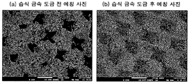
도 6은 옵셋 인쇄 후의 버스바 전극(a)과 습식 금속 도금을 한 후의 버스바 전극(b)의 에칭후 SEM 사진,
도 7은 실시예 1, 실시예 2 및 비교예 1의 방식으로 얻어진 핑거 전극 선폭의 광학 사진(× 100)이다.
** 도면의 주요 부호에 대한 설명 **
1: 기판
2: 버스바 전극
3: 핑거 전극
4: 도금층
이하에서는 도면 및 실시예를 통하여 본 발명을 보다 상세히 설명하기로 한다. 하기의 설명은 본 발명의 구체적 일례에 대한 것이므로, 비록 단정적, 한정적 표현이 있더라도 특허청구범위로부터 정해지는 권리범위를 제한하는 것은 아니다.
본 발명자는 태양광의 차폐를 최소화하고 효율을 높이기 위해서 버스바와 접속된 핑거 전극의 선폭을 줄이고 핑거 전극의 종횡비를 높이는 것이 요구되는데, 이를 실현하기 위한 방법으로서, 옵셋 인쇄 방식으로 태양 전지 전극 패턴을 형성하는 방법을 연구하였다. 그러나 기존의 일반적인 방법으로 옵셋 인쇄를 할 경우, 100㎛이내의 미세 선폭을 요구하는 핑거 전극의 경우에는 원하는 미세 선폭을 얻을 수는 있으나, 버스바 전극과 같이 넓은 선폭을 인쇄할 경우는, 셋 공정이 원활하게 이루어지지 않았다. 그래서 셋 공정이 잘 이루어지기 위한 하나의 방법으로서, 버스바 전극을 도 2a에 도시된 바와 같이 미세 공극이 존재하는 메쉬 형태로 버스바 전극을 형성하게 되면 셋 공정이 원활하게 이루어지고, 동시에 원하는 핑거 전극의 미세 선폭도 함께 구현 할 수 있는 것을 발견하였다.
일반적인 방법으로 옵셋 인쇄시 넓은 선폭에서의 셋 공정이 잘 이루어지지 않는 이유 중 하나는 도 5와 같이 닥터 블레이드(Doctor Blade)가 닥터링(Doctoring)을 수평 방향으로 할 때, 버스바(2)에서 블레이드가 튀는 현상이 발생되는 문제점이 있기 때문이다.
상기 블레이트 튐 문제점을 개선하기 위하여 메쉬 형태로 적용한 경우 인쇄 적성은 향상되었다. 그러나, 인쇄시 도전성 페이스트 층이 메쉬 형상으로 적층되고, 전극 두께가 불균일하여 면 저항과 선 저항 값의 증가되고 소성 후, 실리콘 웨이퍼 층과 도전성 페이스트 층과의 오믹 컨텍 면적 범위가 감소하여 태양 전지 셀 효율을 감소시키는 문제점이 발생하였다.
따라서 상기 옵셋 인쇄 방식을 적용하여 태양 전지 전극을 형성하는 경우에는 전극의 종횡비를 높이고, 태양 전지 셀의 효율을 증가시키기 위하여 옵셋 인쇄를 적어도 2회 이상의 다층으로 구현해야 하는데, 그로 인해 생산 비용이 급격히 상승하는 문제점이 있다. 또한 2회 이상 인쇄하여도 전면 전극용 금속층 내에 금속 입자간 공극으로 전극의 선 저항이 크게 개선되지 않는 문제점이 잔존한다.
이를 종합적으로 해결하기 위해서 본 발명은 옵셋 인쇄 공정으로 기판 위에 선폭이 좁은 도전성 전면 전극을 형성하고, 이 기판을 습식 도금액에 침지하여 도금함으로써 전극을 이루는 금속 전극 내 금속 입자간 공극을 도금 금속으로 메꾸어 준다. 그 결과 핑거(Finger) 전극의 선 저항을 감소시킬 뿐만 아니라, 특히 메쉬 형태의 버스바 전극에 있어서 도전성 페이스트가 적층되지 않은 영역을 도금 금속으로 메워주어 버스바 전극의 오믹컨택 부위를 넓히고 추가적인 열처리 공정으로 치밀화시켜 태양 전지 셀의 효율을 증가시킬 수 있게 된다.
도 1 내지 도 3은 본 발명의 일실시예에 따른, 기판 전면에 형성된 다수의 버스바 전극 및 핑거 전극을 포함하여 이루어진 태양 전지용 기판의 개략 사시도 및 단면도를 제조 수순으로 도시한 도이다. 도시된 바와 같이, 도전성 페이스트를 이용하여 기판(1)에 옵셋 인쇄하여 페이스트 전극으로서의 버스바 전극(2)과 핑거 전극(3)을 형성한 후(도 2), 도금을 통해 도금층(4)을 형성한 것을 특징으로 한다(도 3). 상기 페이스트 전극으로서의 버스바 전극(2)과 핑거 전극(3)은 도금 전에 소성과정을 거칠 수도 있으며, 상기 도금층(4)은 도금 후 열처리 될 수 있다.
상기 기판에 형성된 전극은 다음과 같은 일례의 방법으로 제조될 수 있다. 즉, 기판 상에 버스바 전극 및 핑거 전극을 제조하는 태양 전지용 전극의 제조방법에 있어서, 기판 상에 도전성 페이스트를 사용하여 옵셋(Offset) 방법으로 버스바 전극 및 핑거 전극을 인쇄하는 페이스트 전극 인쇄 단계, 상기 전극 인쇄 단계 후에 습식 도금액에 침지하여 페이스트 전극의 미세 공극 내에 부가적인 금속을 매우는 전극 도금 단계, 및 상기 전극 도금 단계 후에 열처리 하여 오믹 컨텍을 형성하는 열처리 단계를 포함하여 이루어진 것을 특징으로 하는 제조방법에 따라 제조될 수 있다. 상기 페이스트 전극 인쇄 단계와 도금 단계 사이에 페이스트 전극 소성 단계를 더 거칠 수 있다.
상기 전극 인쇄에 사용되는 도전성 페이스트는 본 기술분야에서 알려진 재료를 사용할 수 있으며 제한되지 않는다. 주성분이 은, 구리, 니켈, 알루미늄 등으로 이루어지는 페이스트가 많이 사용되는데 주로, 은 분말이 함유되어 있는 은 페이스트가 사용된다. 구체적으로, 은 분말이 60 내지 85 중량%, 유리 분말이 3 내지 20 중량%, 고분자 바인더가 2 내지 10 중량%, 희석 용제가 3 내지 20 중량% 및 첨가제 0.1 내지 5 중량%로 구성되는 은 페이스트가 옵셋 인쇄에 적합하여 바람직하다.
상기 도전성 페이스트를 인쇄하는 방식으로서는 스크린 인쇄법, 옵셋 인쇄법, 잉크젯 인쇄법 등이 있는데, 잉크젯 인쇄법의 경우에는 인쇄 두께가 5마이크론 미만으로 두께 조절에 제한이 있고, 또한 인쇄에 사용되는 재료의 점성이 50 cPs 이하의 저점도 타입의 재료가 적절하기 때문에, 금속 분말이 60% 이상으로 함유되어 있는 고점도 타입의 도전성 페이스트를 인쇄하기에 적합하지 않다. 스크린 인쇄법의 경우는 주로 많이 사용되나, 형성된 전극의 선폭이 100마이크론 이상으로 비교적 넓어서 태양 전지용 전면 전극으로서 광 조사 시에 전면 전극에 가려지는 비율(차폐율 또는 Shading Loss)이 증가하여 결과적으로 태양 전지 셀 효율이 감소하는 문제점이 생긴다.
따라서 본 발명은 상기 태양 전지용 전면 전극 제조 방법으로서 상기 스크린 인쇄 및 잉크젯 인쇄와 다른 옵셋 인쇄 방식을 적용한 것이 특징이다.
또한 더 바람직한 것으로서, 옵셋 인쇄 방식에 있어서, 도 4와 같이 옵셋 인쇄 적성에 최적화된 메쉬 형태의 버스바 전극 패턴을 적용하여 인쇄시 버스바에서 블레이드가 튀는 현상을 방지하도록 하는 것이 좋다. 본 발명에서 정의하는 메쉬 형태란 미세 공극이 존재하는 패턴이라면 모두 해당되는 것으로서, 그 메쉬의 형상이 사각형, 삼각형, 육각형, 원형, 랜덤 형상이거나 도트 형상일 수 있는 등 다양할 수 있으며 모두 포함된다.
또한, 바람직하게는 태양 전지용 전극 패턴을 도전성 페이스트를 이용하여 옵셋 방법으로 단 1회 인쇄하는 것도 가능하며(1회 인쇄로 본 발명을 제한하는 것은 아니다), 버스바 전극과 핑거 전극을 동시에 인쇄하는 것도 가능하다. 1회 인쇄할 경우, 인쇄 횟수가 적기 때문에 공정이 간단하며, 사용되는 고가의 도전성 페이스트의 양이 적다는 장점이 있다. 다만, 도 6와 같이 메쉬 형태의 버스바 패턴에서 도전성 페이스트가 메꾸어지지 않는 영역으로 인해 버스바 패턴의 면 저항 및 선 저항이 증가되고, 소성 후 실리콘 웨이퍼층과의 오믹 컨텍이 완전히 이루어지지 않아 태양 전지 셀 효율이 감소된다는 문제점이 생길 수 있으나 본 발명에서는 이를 해결하여 우수한 성능의 전극을 얻을 수 있는 특별한 수단이 마련되며 이는 후술한다.
더욱 바람직하기로는 상기 페이스트 전극 인쇄 단계 후에 전극을 소성하는 단계를 추가하는 것이 좋다. 페이스트의 조성에서 소성을 실시하여 고분자 바인더 및 용제 등 절연성 재료를 제거함으로써 전기적 특성을 향상시킬 수 있게 된다. 소성 조건은 제한되지 않으나 600 내지 900℃ 온도에서 수초 내지 수시간 소성하는 것이 좋다.
다음, 도금 공정에 의하여 도전성 페이스트 전극에 부가적인 금속 도금층을 형성한다. 도금 공정에 의하여 도전성 페이스트 전극에 부가적인 금속 도금층을 형성하는데, 도 7과 같이 메쉬 형태의 버스바 패턴의 도전성 페이스트가 적층되지 않는 영역을 도금 금속으로 메우고, 또한 금속 분말 입경이 1 마이크론 이상으로 이루어진 도전성 페이스트 전극의 경우 금속 입자들 간에 공극이 다수 존재하기 때문에 이러한 공극을 치밀한 도금 금속으로서 채워주게 되어, 전극의 면 저항과 선저항을 현저히 감소시키는 효과가 있다. 또한, 상기의 부가적인 습식 금속 도금 공정을 적용함으로서 태양 전지 셀 효율을 증가시키기 위하여 도전성 페이스트를 2회 이상 다층 옵셋 인쇄하지 않아도 되기 때문에 인쇄 횟수만큼 증가하는 고가의 도전성 페이스트 사용량을 저감할 수 있게 된다.
상기 도금 공정의 종류는 제한되지 않으며 습식 금속 도금이 바람직하다. 습식 금속 도금 공정으로는 크게는 무전해 방식과 전해 방식으로 구분 할 수 있다. 무전해 방식은 주로 부도체인 표면에 전도성을 부여하기 위해 사용되는 방법으로서, 금속염과 가용성 환원제가 공존하는 용액에서 환원제의 산화반응으로 방출되는 전자에 의하여 금속이온을 환원시켜 금속을 도금하는 방법이며, 일반적으로 촉매 표면상에서 금속이온의 선택적 환원반응 또는 도금층 금속자체의 촉매작용에 의해 도금이 일어나는 도금 방식이다. 전해도금은 보편적으로 많이 사용하는 방법으로서 피도금물은 반드시 도체 표면이어야만 하고, 이 도체 표면에 외부전원을 이용하여 음극 표면상에 금속을 도금 시키는 방법이다.
본 발명의 바람직한 실시예에 의하면, 도금하고자 하는 피도금물이 도전성 페이스트로 이루어진 전극이므로, 무전해 도금 방식 또는 전해 도금 방식 모두 적용이 가능하기 때문에, 도전성 페이스트 상에 부가적인 금속을 도금하는 방법으로서 무전해 도금 방식이거나 전해 도금 방식, 또는 두가지 도금 방식을 모두 사용하는 것을 포함한다.
또한, 본 발명의 실시예에 의하면, 상기 습식 금속 도금 공정에서의 도금 금속은 비저항 값이 낮은 금속이 사용 가능한데, 제한되지 않으나 은, 금, 구리, 니켈, 주석 등으로 이루어진 군에서 적어도 1종 이상 선택되어질 수 있다.
본 발명은 또한, 바람직한 일실시예로서, 상기 전극 도금 단계 후에 열처리 하여 오믹 컨텍을 형성하는 것이 좋다. 열처리 조건은 제한되지 않으나 400 내지 700도의 온도 범위에서 도금 금속을 수초 내지 수시간 열처리하는 것이 좋다.
상기 열처리는 도금 금속의 치밀화와 연관된다. 열처리 온도가 400도 미만의 경우 공극내 금속 입자의 치밀화가 덜 되어 여전히 공극이 남게 되며, 700도를 넘게 되는 경우 도전성 페이스트의 p-n 접합부분의 뚫림으로 누설 전류가 많이 발생하여 셀 효율이 저하될 수 있다.
상기와 같이 전극을 제조할 경우 핑거 전극의 종횡비(높이/선폭)가 0.2 내지 0.6 범위내로 제조가 가능하며, 한편, 상기 핑거 전극의 선폭은 30㎛ 내지 100㎛ 범위내로 미세 선폭을 만들 수 있고, 높이는 5㎛ 내지 20㎛ 범위내로 제조가 가능하다.
또한, 옵셋 인쇄후에 도금을 실시하지 않은 태양 전지용 전극과 대비하여 볼 때, 도금을 수행한 태양 전지용 전극을 사용한 태양전지가 효율면에서 2배 이상으로 급격히 증가한 것을 확인하였으며, 본 발명의 제조 방법으로 제조된 태양 전지용 전극을 사용한 태양전지는 옵셋 인쇄의 방법을 적용하였음에도 셀 효율(Eff)이 10% 이상이며, 필팩터(FF)가 50% 이상이고, 직렬 저항(Rser)이 0.02Ω 이하로 매우 우수한 전기적 특성을 제공하는 구성적 특징이 있다.
<실시예>
이하 본 발명을 실시예에 의해 상세히 설명한다. 단, 하기 실시예는 본 발명을 예시하는 것일 뿐, 본 발명의 내용이 하기 실시예에 한정되는 것은 아니다.
실시예 1
먼저 옵셋용 페이스트 조성물(은분말 68%, 유리프리트 17%, 바인더 10%, 희석용제 3%, 분산제 및 기타 2%)을 이용하여 그라비아 옵셋 인쇄하였다. 초기 그라비아 롤의 블레이드 압력, 각도로 닥터링 상태를 체크하고, 블랑켓 롤의 오프닙(Off nip)과 셋닙(Setnip) 조절을 통해 오프 압과 셋 압을 최적 상태로 조절하였다. 상기 그라비아 롤과 블레이드 사이에 페이스트 20g을 넣은 후 약 7rpm으로 닥터링을 하였다. 3회 이상 닥터링을 한 후 블랑켓 롤에 있는 러버에 페이스트를 7rpm으로 오프시킨 후 블랑켓 롤을 1회전을 시켰다. 블랑켓 롤이 1회전 하는 동안 러버에서 충분히 흡수된 페이스트는 7rpm 속도로 셋을 하였다. 이와 같은 방식으로 인쇄판에 진공으로 고정된 5〃웨이퍼에 도전성 페이스트를 1회 인쇄 하였다. 인쇄한 기판을 건조한 후 적외선 로에서 190rpm의 속도로 약 800℃에서 20초 동안 소성시켰다. 그 후, 배면 전극인 알루미늄 전극층에 전해도금 하기 위한 전류 통전 부분을 연결하고, 통전 부분을 제외한 배면 전극 전체를 도금액의 침투를 방지하기 위해 마스킹하여 습식 금속 도금을 실시하였다. 습식 금속 도금 공정으로서 전해 은 도금을 실시하였는데, 은 금속염으로서 시안화 은 칼륨 25g/l, 금속 착염을 위한 시안화칼륨 75g/l, 전해도금 시의 전기전도도 및 전착 균일성을 위한 탄산 칼륨 30g/l, 도금막의 치밀도 및 광택을 위한 첨가제 Argalux64 (Atotec Korea 製)4g/l로 이루어진 전해 은 도금 욕에 침지하고, 양극으로서 은 플레이트를 사용하여 전류를 인가하여 욕 온도 25도, 전류밀도 1.0A/dm2, 도금시간 10분의 조건에서 은 도금층을 성막하였다. 그리고 상기 도금한 웨이퍼를 550도씨에서 10분간 열처리하여 태양 전지용 전극을 형성하였다. 그 후, I-V 테스트기(PASAN製, CT801)에 넣고 셀 효율, 필팩터, Voc, Isc, 직렬 저항 및 션트 저항을 측정하여 표 1에 나타내었다.
태양 전지 셀을 평가하기 위하여 I-V 테스트기로 측정하는데, 주요 측정 인자는 개방전압(Voc), 단락전류(Isc), 필팩터(FF), 셀 효율(%), 직렬저항(Rser), 병렬저항(Rsh)이다. 여기서 Voc는 일정한 온도와 일조 강도에서 부하가 연결되지 않은 개방 상태에서 셀 양단에 걸리는 전압을 가리키며, Isc는 일정 온도와 일조 강도에서 단락 상태로 셀에서 출력되는 전류를 가리킨다. FF는 셀 효율과 연관되는데 먼저 셀 효율은 태양으로부터 입사된 태양에너지[Watt]를 기준으로 셀이 얼마만큼의 에너지[Watt]를 만들 수 있는지 척도가 되는 인자이다. 필팩터가 100%인 경우는 I-V 커브에서 완전 사각형 형태를 나타내며, Isc와 Voc의 값만 곱해서 이상적인 전력(Pmax)를 얻게 되나, 실제 상기 셀 내부의 직렬저항과 병렬저항에 의해 필팩터가 떨어지게 되어 충분한 Pmax를 내기 어려워진다. 필팩터를 떨어뜨리는 요소 중 특히 상기 직렬저항 부분이 중요한데, 보통 직렬저항은 Isc에 큰 영향을 끼친다. 직렬저항은 기판 저항, 실리콘과 전면 전극의 컨택 저항, 에미터 저항, 전극 금속 자체의 저항의 합으로 구성된다. 일반적으로 셀 효율은 직렬 저항값이 낮고, 필팩터가 높은 경우 높은 값을 나타낸다.
실시예 2
상기 실시예 1에서 습식 금속 도금 공정으로서 전해 동 도금과 무전해 은 도금을 실시한 것 외에 실시예 1과 동일하게 진행하였다. 이때 전해동 도금은 금속염으로서 황산구리 220g/l, 황산 60ml/l 으로 이루어진 전해동 도금 욕에 침지하고, 양극으로서 동 플레이트를 사용하여 전류를 인가하여 욕 온도 25도, 전류밀도 0.5A/dm2, 도금시간 10분의 조건에서 전해 동 도금층을 성막하였다. 그리고, 상기 실시예 1에서 사용한 은 도금욕에 침지하여 전류를 인가하지 않고 동 도금층과 은 도금욕의 금속 이온화 경향 차이에 따른 치환도금 방식의 원리를 이용하여 5분 침지하여 최종적으로 무전해은 도금층을 성막시켰다.
비교예 1
상기 실시예 1과 같이 동일한 방식으로 도전성 페이스트를 1회 옵셋 인쇄하고 소성한 후에, 습식 금속 도금 공정을 행하지 않고 I-V 테스트기(PASAN製, CT801)에 넣고 셀 효율, 필팩터, Voc, Isc, 직렬 저항 및 션트 저항을 측정하였다.
표 1
| 실시예 1 | 실시예 2 | 비교예 1 | |
| 도금 금속 종류 | Ag | Cu-Ag | 無 |
| 도금 금속 두께[㎛] | 5.51 | 7.25 | 無 |
| 총 핑거 전극 선폭[㎛] | 52.17 | 56.91 | 31.84 |
| 총 핑거 전극 높이[㎛] | 10.35 | 11.83 | 4.50 |
| 핑거 전극 종횡비(높이/선폭) | 0.20 | 0.21 | 0.14 |
| 셀 효율[%] | 14.7 | 15.42 | 6.21 |
| 필팩터[%] | 67.22 | 70.45 | 35.87 |
| Isc[A] | 5.456 | 5.463 | 4.357 |
| Voc[V] | 0.621 | 0.621 | 0.615 |
| Rser[Ω] | 0.0150 | 0.0115 | 0.0594 |
| Rsht[Ω] | 7.3 | 10.6 | 0.3 |
상기, 표 1에 나타난 바와 같이 반도체 웨이퍼 위에 도전성 페이스트를 옵셋 방법으로 1회 인쇄하고 소성하여 도전성 페이스트 전극을 형성한 후, 습식 금속 도금을 실시하지 않은 비교예 1과 습식 금속 도금을 실시한 실시예 1 및 2에서 만들어진 셀을 비교한 결과, 습식 금속 도금을 실시한 셀의 핑거 전극의 종횡비가 크며, 셀의 전기적 특성인 효율도 더 좋은 결과를 나타내고 있다.
본 발명에 의한 태양 전지용 전극 형성 방법은 간단하고 생산성이 높으며 버스바 전극의 면저항을 감소시켜주며, 핑거 전극 선폭을 100 마이크론 이내로 구현할 수 있고 또한 전극의 종횡비를 0.2 내지 0.6으로 구현하여 빛의 차폐율 줄이고, 도금 후 열처리를 통한 도금 금속과 실리콘 웨이퍼 층과의 부가적인 오믹 컨텍 형성으로 태양 전지 셀의 효율을 향상시킬 수 있어 산업적으로 유용하다.
Claims (12)
- 기판 전면에 형성된 다수의 버스바 전극 및 핑거 전극을 포함하여 이루어진 태양 전지용 기판에 있어서,상기 버스바 전극 및 핑거 전극은 도전성 페이스트를 이용하여 옵셋 인쇄된 후 도금되어 형성된 것을 특징으로 하는 태양 전지용 기판.
- 제1항에 있어서, 상기 버스바 전극은 미세 공극이 존재하는 메쉬 형상으로 옵셋 인쇄되는 것을 특징으로 하는 태양 전지용 기판.
- 제1항에 있어서, 상기 옵셋 인쇄는 단 1회 수행되며, 버스바 전극과 핑거 전극을 동시에 인쇄하는 것을 특징으로 하는 태양 전지용 기판.
- 제1항에 있어서, 상기 옵셋 인쇄 후에 소성한 뒤 상기 도금을 실시한 것을 특징으로 하는 태양 전지용 기판.
- 제1항에 있어서, 상기 도금 후에 도금 금속을 열처리하는 것을 특징으로 하는 태양 전지용 기판.
- 제1항에 내지 제5항 중 어느 한 항에 있어서, 상기 핑거 전극의 종횡비(높이/선폭)는 0.2 내지 0.6 범위내인 것을 특징으로 하는 태양 전지용 기판.
- 제1항에 내지 제5항 중 어느 한 항에 있어서, 상기 핑거 전극의 선폭은 30㎛ 내지 100㎛ 범위내이며, 높이는 5㎛ 내지 20㎛ 범위내인 것을 특징으로 하는 태양 전지용 기판.
- 제1항에 내지 제5항 중 어느 한 항의 태양 전지용 기판을 사용하여 제조된 태양 전지로서, 상기 옵셋 인쇄후에 도금을 실시하지 않고 전극을 형성하여 제조된 태양 전지용 기판을 사용한 태양 전지와 대비하여 볼 때, 효율이 2배 이상인 것을 특징으로 하는 태양 전지.
- 기판 상에 버스바 전극 및 핑거 전극을 제조하는 태양 전지용 전극의 제조방법에 있어서,기판 상에 도전성 페이스트를 사용하여 옵셋(Offset) 방법으로 버스바 전극 및 핑거 전극을 인쇄하는 페이스트 전극 인쇄 단계;상기 전극 인쇄 단계 후에 습식 도금액에 침지하여 페이스트 전극의 미세 공극 내에 부가적인 금속을 매우는 전극 도금 단계; 및상기 전극 도금 단계 후에 열처리 하여 오믹 컨텍을 형성하는 열처리 단계;를 포함하여 이루어진 태양 전지용 전극의 제조방법.
- 제9항에 있어서, 상기 페이스트 전극 인쇄 단계 후에 전극을 소성하는 단계를 추가하는 것을 특징으로 하는 태양 전지용 전극의 제조방법.
- 제9항에 있어서, 상기 버스바 전극은 미세 공극이 존재하는 메쉬 형상으로 옵셋 인쇄되는 것을 특징으로 하는 태양 전지용 전극의 제조 방법.
- 제9항 내지 제11항 중 어느 한 항의 태양 전지용 전극의 제조 방법을 이용하여 제조된 태양 전지 전극을 구비한 태양 전지로서, 셀 효율(Eff)이 10% 이상이며, 필팩터(FF)가 50% 이상이고, 직렬 저항(Rser)이 0.02Ω 이하인 것을 특징으로 하는 태양 전지.
Priority Applications (4)
| Application Number | Priority Date | Filing Date | Title |
|---|---|---|---|
| CN200980146120XA CN102217088A (zh) | 2008-11-18 | 2009-11-18 | 太阳能电池用电极的制造方法、利用该方法制造的太阳能电池用基板及太阳能电池 |
| JP2011537357A JP2012509588A (ja) | 2008-11-18 | 2009-11-18 | 太陽電池用電極の製造方法、これを用いて製造された太陽電池用基板及び太陽電池 |
| EP09827715A EP2355167A2 (en) | 2008-11-18 | 2009-11-18 | Method for manufacturing electrode for solar cell, substrate for solar cell manufactured by the same, and solar cell manufactured by the same |
| US13/110,659 US20110214734A1 (en) | 2008-11-18 | 2011-05-18 | Method for manufacturing electrode for solar cell, substrate for solar cell manufactured by the same, and solar cell manufactured by the same |
Applications Claiming Priority (2)
| Application Number | Priority Date | Filing Date | Title |
|---|---|---|---|
| KR1020080114344A KR101133028B1 (ko) | 2008-11-18 | 2008-11-18 | 태양 전지용 전극의 제조방법, 이를 이용하여 제조된 태양 전지용 기판 및 태양 전지 |
| KR10-2008-0114344 | 2008-11-18 |
Related Child Applications (1)
| Application Number | Title | Priority Date | Filing Date |
|---|---|---|---|
| US13/110,659 Continuation US20110214734A1 (en) | 2008-11-18 | 2011-05-18 | Method for manufacturing electrode for solar cell, substrate for solar cell manufactured by the same, and solar cell manufactured by the same |
Publications (2)
| Publication Number | Publication Date |
|---|---|
| WO2010058950A2 true WO2010058950A2 (ko) | 2010-05-27 |
| WO2010058950A3 WO2010058950A3 (ko) | 2010-08-05 |
Family
ID=42198653
Family Applications (1)
| Application Number | Title | Priority Date | Filing Date |
|---|---|---|---|
| PCT/KR2009/006783 Ceased WO2010058950A2 (ko) | 2008-11-18 | 2009-11-18 | 태양 전지용 전극의 제조방법, 이를 이용하여 제조된 태양 전지용 기판 및 태양 전지 |
Country Status (6)
| Country | Link |
|---|---|
| US (1) | US20110214734A1 (ko) |
| EP (1) | EP2355167A2 (ko) |
| JP (1) | JP2012509588A (ko) |
| KR (1) | KR101133028B1 (ko) |
| CN (1) | CN102217088A (ko) |
| WO (1) | WO2010058950A2 (ko) |
Cited By (1)
| Publication number | Priority date | Publication date | Assignee | Title |
|---|---|---|---|---|
| EP2595196A4 (en) * | 2010-06-25 | 2017-04-19 | Kyocera Corporation | Solar cell element, process for producing same, and solar cell module |
Families Citing this family (19)
| Publication number | Priority date | Publication date | Assignee | Title |
|---|---|---|---|---|
| KR20100066817A (ko) * | 2008-12-10 | 2010-06-18 | 에스에스씨피 주식회사 | 태양 전지용 전극의 제조방법, 이를 이용하여 제조된 태양 전지용 기판 및 태양 전지 |
| KR101138174B1 (ko) * | 2010-09-09 | 2012-04-25 | 현대중공업 주식회사 | 태양전지의 후면전극 형성방법 |
| KR101275576B1 (ko) * | 2010-12-28 | 2013-06-14 | 엘지전자 주식회사 | 태양전지 및 이의 제조 방법 |
| TWI584485B (zh) * | 2011-10-29 | 2017-05-21 | 西瑪奈米技術以色列有限公司 | 於基材上對齊的網路 |
| TWI497731B (zh) * | 2011-12-15 | 2015-08-21 | Au Optronics Corp | 太陽能電池及太陽能發電模組 |
| DE202012004369U1 (de) * | 2012-04-30 | 2012-05-14 | Solarworld Innovations Gmbh | Photovoltaikmodul |
| KR101371865B1 (ko) * | 2012-10-16 | 2014-03-10 | 현대중공업 주식회사 | 태양전지의 전면전극 구조 및 그 제조방법 |
| CN102931245A (zh) * | 2012-11-28 | 2013-02-13 | 山东力诺太阳能电力股份有限公司 | 太阳电池正面栅线及印刷该正面栅线的太阳能电池片 |
| CN104015471A (zh) * | 2013-03-01 | 2014-09-03 | 昆山允升吉光电科技有限公司 | 一种太阳能丝网 |
| DE102013113108B4 (de) * | 2013-11-27 | 2024-08-29 | Hanwha Q Cells Gmbh | Solarzellenherstellungsverfahren |
| DE102013113123B4 (de) * | 2013-11-27 | 2021-11-18 | Hanwha Q Cells Gmbh | Solarzellenherstellungsverfahren |
| US20150333197A1 (en) * | 2014-05-13 | 2015-11-19 | E I Du Pont De Nemours And Company | Method of manufacturing a solar cell electrode |
| KR20160002581A (ko) | 2014-06-30 | 2016-01-08 | 주식회사 네패스 | 나노 와이어를 이용한 패턴 형성 방법 |
| JP2017533596A (ja) * | 2014-10-31 | 2017-11-09 | ビーワイディー カンパニー リミテッドByd Company Limited | 太陽電池ユニット、太陽電池アレイ、太陽電池モジュール、及びこれらの製造方法 |
| US10529868B2 (en) | 2014-10-31 | 2020-01-07 | Byd Company Limited | Solar cell array, solar cell module and manufacturing method thereof |
| KR101637825B1 (ko) * | 2015-04-06 | 2016-07-07 | 현대중공업 주식회사 | 태양전지의 후면전극 구조 및 그 제조방법 |
| CN112747844B (zh) * | 2020-12-22 | 2022-04-29 | 北京航空航天大学杭州创新研究院 | 一种三明治结构触觉传感阵列制备方法 |
| TW202518607A (zh) * | 2023-10-30 | 2025-05-01 | 強茂股份有限公司 | 預成型封裝導線架的製造方法 |
| CN119302057A (zh) | 2023-11-24 | 2025-01-10 | 中建材玻璃新材料研究院集团有限公司 | 基于表面修改的金属网格横纵比优化方法 |
Family Cites Families (15)
| Publication number | Priority date | Publication date | Assignee | Title |
|---|---|---|---|---|
| JPS5929474A (ja) * | 1982-08-11 | 1984-02-16 | Toshiba Corp | 太陽電池 |
| JPS59194494A (ja) * | 1983-04-18 | 1984-11-05 | 松下電器産業株式会社 | セラミツク多層配線基板の製造法 |
| JPH01152459A (ja) * | 1987-12-09 | 1989-06-14 | Mitsubishi Heavy Ind Ltd | 印刷方法 |
| JPH08148709A (ja) * | 1994-11-15 | 1996-06-07 | Mitsubishi Electric Corp | 薄型太陽電池の製造方法及び薄型太陽電池の製造装置 |
| JP3904317B2 (ja) | 1998-02-05 | 2007-04-11 | 住友ゴム工業株式会社 | プリント基板の製造方法 |
| JPH11307910A (ja) | 1998-04-21 | 1999-11-05 | Mitsumura Printing Co Ltd | 導電性パターン及びその形成方法 |
| JP2000277768A (ja) * | 1999-03-25 | 2000-10-06 | Kyocera Corp | 太陽電池の形成方法 |
| JP2004193337A (ja) * | 2002-12-11 | 2004-07-08 | Sharp Corp | 太陽電池の電極形成方法およびその方法により製造される太陽電池 |
| JP2005175321A (ja) | 2003-12-12 | 2005-06-30 | Hitachi Ltd | エッチングレジスト前駆体組成物及びそれを用いた配線基板の製造方法、並びに配線基板 |
| JP2005203484A (ja) * | 2004-01-14 | 2005-07-28 | Morimura Chemicals Ltd | 導電回路装置および導電回路装置の製造方法 |
| JP2006339342A (ja) * | 2005-06-01 | 2006-12-14 | Shin Etsu Handotai Co Ltd | 太陽電池および太陽電池の製造方法 |
| JP4425246B2 (ja) * | 2005-08-31 | 2010-03-03 | 三洋電機株式会社 | 光起電力装置および光起電力装置の製造方法 |
| US20080216887A1 (en) * | 2006-12-22 | 2008-09-11 | Advent Solar, Inc. | Interconnect Technologies for Back Contact Solar Cells and Modules |
| JP4818094B2 (ja) * | 2006-12-22 | 2011-11-16 | 三洋電機株式会社 | 太陽電池集電極の形成装置及び太陽電池集電極の形成方法 |
| US20090159119A1 (en) * | 2007-03-28 | 2009-06-25 | Basol Bulent M | Technique and apparatus for manufacturing flexible and moisture resistive photovoltaic modules |
-
2008
- 2008-11-18 KR KR1020080114344A patent/KR101133028B1/ko not_active Expired - Fee Related
-
2009
- 2009-11-18 EP EP09827715A patent/EP2355167A2/en not_active Withdrawn
- 2009-11-18 JP JP2011537357A patent/JP2012509588A/ja not_active Ceased
- 2009-11-18 CN CN200980146120XA patent/CN102217088A/zh active Pending
- 2009-11-18 WO PCT/KR2009/006783 patent/WO2010058950A2/ko not_active Ceased
-
2011
- 2011-05-18 US US13/110,659 patent/US20110214734A1/en not_active Abandoned
Cited By (1)
| Publication number | Priority date | Publication date | Assignee | Title |
|---|---|---|---|---|
| EP2595196A4 (en) * | 2010-06-25 | 2017-04-19 | Kyocera Corporation | Solar cell element, process for producing same, and solar cell module |
Also Published As
| Publication number | Publication date |
|---|---|
| WO2010058950A3 (ko) | 2010-08-05 |
| US20110214734A1 (en) | 2011-09-08 |
| JP2012509588A (ja) | 2012-04-19 |
| KR20100055558A (ko) | 2010-05-27 |
| KR101133028B1 (ko) | 2012-04-04 |
| CN102217088A (zh) | 2011-10-12 |
| EP2355167A2 (en) | 2011-08-10 |
Similar Documents
| Publication | Publication Date | Title |
|---|---|---|
| WO2010058950A2 (ko) | 태양 전지용 전극의 제조방법, 이를 이용하여 제조된 태양 전지용 기판 및 태양 전지 | |
| WO2010068050A9 (ko) | 태양 전지용 전극의 제조방법, 이를 이용하여 제조된 태양 전지용 기판 및 태양 전지 | |
| KR20110123663A (ko) | 솔루션 기반의 프로세스에 의한 광전지 그리드 스택 방법 및 구조 | |
| JPWO2012105381A1 (ja) | 太陽電池用スクリーン製版及び太陽電池の電極の印刷方法 | |
| WO2010117207A2 (en) | Paste and solar cell using the same | |
| CN102804389A (zh) | 在硅片正面上形成栅阴极的方法 | |
| EP2227830A2 (en) | Solar cell, mehtod of manufacturing the same, and method of texturing solar cell | |
| WO2011046365A2 (ko) | 은 페이스트 조성물 및 이를 이용한 태양전지 | |
| EP2662883B1 (en) | Composition for forming p-type diffusion layer, method for forming p-type diffusion layer, and method for producing photovoltaic cell | |
| KR101149891B1 (ko) | 태양전지 및 이의 제조방법 | |
| WO2018080094A1 (ko) | 태양전지 전극용 도전성 페이스트 및 이를 사용하여 제조된 태양전지 | |
| JP5428940B2 (ja) | オフセット印刷装置及び該装置を用いた太陽電池の電極形成方法 | |
| CN106098146A (zh) | 高效晶体硅太阳能电池局域背场铝浆及在perc电池中的应用 | |
| TW201242040A (en) | Method for manufacturing solar cell element and solar cell element | |
| WO2020111900A1 (ko) | 태양전지 전극용 도전성 페이스트 및 이를 사용하여 제조된 태양전지 | |
| JP2010165944A (ja) | 光起電力装置とその製造方法および光起電力装置の製造装置 | |
| WO2019088520A2 (ko) | 태양전지 전극용 도전성 페이스트 및 이에 포함되는 유리 프릿, 그리고 태양 전지 | |
| WO2020111905A1 (ko) | 태양전지 전극용 도전성 페이스트 및 이를 이용하여 제조된 태양 전지 | |
| EP3702048B1 (en) | Method for drying polyimide paste and method for producing solar cells capable of highly-efficient photoelectric conversion | |
| JP5625538B2 (ja) | p型拡散層形成組成物、p型拡散層の製造方法、及び太陽電池セルの製造方法 | |
| CN106159022B (zh) | 一种晶体硅太阳能电池片及其制备方法 | |
| Lin et al. | Cost-Effective Metallization of N-Type TOPCon Solar Cells Using Ag-Coated Copper Paste | |
| US20140227821A1 (en) | P-type diffusion layer forming composition | |
| WO2021194060A1 (ko) | 태양전지 전극용 도전성 페이스트 및 이를 이용하여 제조된 태양 전지 | |
| WO2018080095A1 (ko) | 태양전지 전극용 도전성 페이스트 및 이를 사용하여 제조된 태양전지 |
Legal Events
| Date | Code | Title | Description |
|---|---|---|---|
| WWE | Wipo information: entry into national phase |
Ref document number: 200980146120.X Country of ref document: CN |
|
| 121 | Ep: the epo has been informed by wipo that ep was designated in this application |
Ref document number: 09827715 Country of ref document: EP Kind code of ref document: A2 |
|
| WWE | Wipo information: entry into national phase |
Ref document number: 2009827715 Country of ref document: EP |
|
| NENP | Non-entry into the national phase |
Ref country code: DE |
|
| WWE | Wipo information: entry into national phase |
Ref document number: 2011537357 Country of ref document: JP |