WO2010074176A1 - 電力供給装置 - Google Patents
電力供給装置 Download PDFInfo
- Publication number
- WO2010074176A1 WO2010074176A1 PCT/JP2009/071491 JP2009071491W WO2010074176A1 WO 2010074176 A1 WO2010074176 A1 WO 2010074176A1 JP 2009071491 W JP2009071491 W JP 2009071491W WO 2010074176 A1 WO2010074176 A1 WO 2010074176A1
- Authority
- WO
- WIPO (PCT)
- Prior art keywords
- electronic switch
- power supply
- voltage
- turned
- motor
- Prior art date
- Legal status (The legal status is an assumption and is not a legal conclusion. Google has not performed a legal analysis and makes no representation as to the accuracy of the status listed.)
- Ceased
Links
Images

Classifications
-
- H—ELECTRICITY
- H02—GENERATION; CONVERSION OR DISTRIBUTION OF ELECTRIC POWER
- H02P—CONTROL OR REGULATION OF ELECTRIC MOTORS, ELECTRIC GENERATORS OR DYNAMO-ELECTRIC CONVERTERS; CONTROLLING TRANSFORMERS, REACTORS OR CHOKE COILS
- H02P7/00—Arrangements for regulating or controlling the speed or torque of electric DC motors
- H02P7/06—Arrangements for regulating or controlling the speed or torque of electric DC motors for regulating or controlling an individual DC dynamo-electric motor by varying field or armature current
- H02P7/18—Arrangements for regulating or controlling the speed or torque of electric DC motors for regulating or controlling an individual DC dynamo-electric motor by varying field or armature current by master control with auxiliary power
- H02P7/24—Arrangements for regulating or controlling the speed or torque of electric DC motors for regulating or controlling an individual DC dynamo-electric motor by varying field or armature current by master control with auxiliary power using discharge tubes or semiconductor devices
- H02P7/28—Arrangements for regulating or controlling the speed or torque of electric DC motors for regulating or controlling an individual DC dynamo-electric motor by varying field or armature current by master control with auxiliary power using discharge tubes or semiconductor devices using semiconductor devices
- H02P7/285—Arrangements for regulating or controlling the speed or torque of electric DC motors for regulating or controlling an individual DC dynamo-electric motor by varying field or armature current by master control with auxiliary power using discharge tubes or semiconductor devices using semiconductor devices controlling armature supply only
- H02P7/29—Arrangements for regulating or controlling the speed or torque of electric DC motors for regulating or controlling an individual DC dynamo-electric motor by varying field or armature current by master control with auxiliary power using discharge tubes or semiconductor devices using semiconductor devices controlling armature supply only using pulse modulation
Definitions
- the present invention relates to a power supply device that controls electric power supplied to a motor load by PWM control of an electronic switch with a desired duty ratio, and more particularly to a technique for reducing energy loss due to heat generation.
- a load circuit that provides an electronic switch such as a MOSFET between a DC power source and a load, adjusts the power supplied to the load by PWM control of the MOSFET, and controls the output of the load is often used (for example, see Patent Document 1).
- FIG. 4 is a circuit diagram showing a configuration of a load circuit for driving a motor M101 used for a radiator fan or the like mounted on a vehicle by PWM control, and a plus terminal of a DC power supply VB (for example, a battery mounted on the vehicle)
- An electronic switch T101 such as a MOSFET is provided between the motor M101 and the motor M101.
- the inductance of the motor M101 is LM and the armature resistance is Ra.
- the gate of the electronic switch T101 is connected to the driver 102 via the resistor R101.
- a charge pump 101 is connected to the driver 102.
- the driver 102 When an input signal that is repeatedly turned on and off at a predetermined cycle is supplied to the driver 102, the driver 102 outputs the output voltage of the charge pump 101 to the gate of the electronic switch T101, and the electronic switch T101 is PWM driven with a duty ratio.
- the electronic switch T101 is turned on, the positive terminal of the DC power source VB ⁇ the electronic switch T101 ⁇ the motor M101 ⁇ the ground.
- ⁇ ID IM when current flows through the negative terminal of the DC power supply VB.
- the inductance LM of the motor M101 the electromagnetic energy of the LM * IM 2/2 is accumulated.
- a flywheel diode D101 (hereinafter simply referred to as “diode”) is provided in parallel with the motor M101.
- the power loss generated in the diode D101 is represented by VF * IF, where VF is the forward voltage drop of the diode D101. This power loss is converted into heat and only increases the temperature of the diode D101, and does not contribute to the maintenance of the rotational speed of the motor M101.
- the present invention has been made to solve such a conventional problem, and an object of the present invention is to be able to reduce the energy loss caused by the forward voltage of the flywheel diode. It is to provide a supply device.
- the electronic switch (T1) provided on the wiring connecting the DC power supply (VB) and the motor load (M1), and the electronic switch are PWM-controlled to control the electronic switch.
- a semiconductor comprising a drive unit for driving a motor load, and a parasitic diode arranged in parallel to the motor load so that a direction opposite to a current flowing through the motor load is a forward direction of the parasitic diode
- a power supply device including an element (T2) and a control unit that performs control to turn on the semiconductor element in a part of a period in which the electronic switch is turned off by the PWM control.
- the partial period is set to the electronic switch. From the time when the voltage at the first connection point (point a) connecting the electronic switch and the motor load drops below the ground level after the electromagnetic switch is turned off. The period between the time before the voltage starts to rise.
- the semiconductor element (T2) includes a first main electrode connected to a first connection point connecting the electronic switch and the motor load, a second main electrode connected to the ground, and a control.
- a control electrode to which a signal is input wherein the semiconductor element is turned on when a positive voltage is applied to the control electrode, and the control unit moves the electronic switch from on to off and the first connection
- the application of the positive voltage to the control electrode is started, and the first time from when the positive voltage is applied until the voltage at the first connection point starts to rise.
- the application of the positive voltage is stopped when the shorter period of the period or the second period from the application of the positive voltage to the lapse of a fixed time has elapsed.
- the semiconductor element (T2) is an N-type field effect transistor
- the first main electrode is a drain
- the second main electrode is a source
- the control electrode is a gate
- the control unit Has a series connection circuit of a first resistor (R2) and a transistor (T3) disposed between the DC power supply and the ground, and a control input terminal of the transistor (T3) is connected to the first connection point.
- a second connection point (point b) to which the first resistor (R2) and the transistor (T3) are connected is grounded through a series connection circuit of a capacitor (C1) and a second resistor (R3).
- a third connection point (point c) to which the capacitor (C1) and the second resistor (R3) are connected is connected to the gate of the semiconductor element (T2).
- control unit includes an inverter circuit that generates an inverted signal of the PWM signal, a delay circuit that delays an output signal of the inverter circuit for a predetermined time, and a rising timing of the PWM signal output from the delay circuit And a one-shot multivibrator that outputs an ON signal for a predetermined time.
- a semiconductor element (T2) such as a MOSFET is provided in parallel to the motor load (M1), and when the motor load is driven by PWM control of the electronic switch (T1).
- the semiconductor element (T2) is turned on during a part of the period when the electronic switch (T1) is off. Accordingly, the return current flowing through the motor load (M1) flows through the semiconductor element (T2), and heat generation can be reduced as compared with the case where a conventional flywheel diode is used. Loss can be reduced.
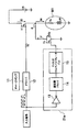
- FIG. 1 is a circuit diagram showing a configuration of a load circuit including a power supply device according to the first embodiment of the present invention.
- the load circuit according to this embodiment includes a DC power supply VB such as a battery mounted on a vehicle, an electronic switch T1 such as a MOSFET, and a motor M1 (for driving a radiator fan). (Motor load) series connection circuit.
- the gate of the electronic switch T1 is connected to the driver 12 via the resistor R1, and the driver 12 is supplied with power from the charge pump 11.
- an N-type MOSFET (T2; semiconductor element) is provided in parallel with the motor M1.
- the drain (first main electrode) of the MOSFET (T2) is connected to a point (first connection point) that is a connection point between the electronic switch T1 and the motor M1, and the source (second main electrode) is connected to the ground. It is connected.
- the parasitic diode Dp of the MOSFET (T2) has a cathode connected to the point a and an anode connected to the ground.
- the gate (control electrode) of the MOSFET (T2) is connected to the control circuit 21 and is controlled to be turned on and off by the control circuit 21.
- the control circuit 21 includes a transistor T3 (which is a MOSFET in this embodiment), a resistor R2 (first resistor), R3 (second resistor), a capacitor C1, and a diode D2.
- One end of the resistor R2 is connected to the plus terminal of the DC power supply VB, and the other end is connected to the ground via the transistor T3.
- a point b (second connection point) that is a connection point between the resistor R2 and the transistor T3 is connected to one end of the capacitor C1.
- the gate of the transistor T3 is connected to the point a.
- the point c which is the other end of the capacitor C1 is connected to the gate of the MOSFET (T2), is connected to the ground via the resistor R3, and is further connected to the cathode of the diode D2. .
- the anode of the diode D2 is connected to the ground.
- control circuit 21 reduces the heat generation of the parasitic diode Dp by turning on the MOSFET (T2) during a part of the period in which the electronic switch T1 is turned off, thereby reducing the energy loss. To reduce.
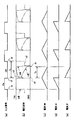
- FIGS. 3A to 3E are timing charts showing waveforms of signals of the power supply circuit according to the first embodiment.
- FIG. 3A is a waveform of an input signal supplied to the driver 12.
- 3B is a voltage waveform generated at points a, b and c
- FIG. 3C is a waveform of current IM flowing through the motor M1
- FIG. 3D is a waveform of current ID flowing through the electronic switch T1.
- FIG. 3E shows the return current IF flowing through the MOSFET (T2) or the parasitic diode Dp.
- the electronic switch T1 when a PWM signal is output from the driver 12 and a drive signal is supplied to the gate of the electronic switch T1, the electronic switch T1 is repeatedly turned on and off at a predetermined duty ratio. That is, as shown in FIG. 3A, the electronic switch T1 is repeatedly turned on and off at a constant cycle.
- the electronic switch T1 is turned on at time t1 shown in FIG. 3A, the voltage at the point a rises to almost the output voltage of the DC power supply VB as shown in FIG. 3B.
- the current ID flowing through the electronic switch T1 gradually increases.
- the current IM flowing through the motor M1 gradually increases.
- the gate voltage of the transistor T3 increases, the transistor T3 is turned on, and the point b is connected to the ground.
- the voltage at the point c which is the gate of the MOSFET (T2) is a voltage which is pushed down by the forward voltage of the diode D2 (this is referred to as VF2) from the ground level, and the MOSFET (T2) is turned off. That is, when the electronic switch T1 is turned on, the MOSFET (T2) is turned off.
- the parasitic diode Dp included in the MOSFET (T2), and further reduction is limited ( (See symbol q1 in FIG. 3B). That is, the parasitic diode Dp functions as a flywheel diode.
- the transistor T3 is turned off, and the connection between the point b and the ground is cut off, so that the voltage at the point b increases.
- the voltage at the point c increases at a voltage lower by about 0.7 V than the point b (see t2 to t3 in FIG. 3).
- the MOSFET (T2) When the voltage at the point c rises, the MOSFET (T2) is turned on, and the return current IF of the motor M1 bypasses the parasitic diode Dp, and follows the path of the motor M1, the ground, the MOSFET (T2), the point a, and the motor M1.
- the power loss due to the parasitic diode Dp is replaced with the power loss due to the on-resistance of the MOSFET (T2).
- the on-resistance of the MOSFET (T2) is 5 [m ⁇ ] and the return current IF is 10 A, the power loss is 0.5 W.
- the power loss is 7 W when a reflux current of 10 A flows, so that the power loss is reduced by using the MOSFET (T2). 1/14.
- the return current reaches its maximum value when the electronic switch T1 is turned off, and thereafter decreases with a constant gradient. Therefore, the power loss also decreases rapidly in proportion to the square of the return current IF (IF 2 ).
- the MOSFET (T2) since the MOSFET (T2) is turned off when the electromagnetic energy accumulated in the inductance LM of the motor M1 disappears, it is possible to prevent the inertial energy of the armature from being wasted. Furthermore, the MOSFET (T2) can be reliably turned off at a time before time t5 when the electronic switch T1 is turned on next time.
- the return current IF flows through the parasitic diode Dp. At this time, there is a concern about power loss due to the parasitic diode Dp. However, since the return current IF decreases after the time determined by the time constant ⁇ , the power loss due to the parasitic diode Dp becomes extremely small. .
- the MOSFET (T2) is provided in parallel to the motor M1.
- the MOSFET (T2) is turned on during a part of the period in which the electronic switch T1 is turned off. Therefore, when the electronic switch T1 is turned off, the return current IF flowing through the motor M1 is returned via the MOSFET (T2). In contrast, energy loss can be significantly reduced.
- the MOSFET (T2) is turned on after the electronic switch T1 is turned off, and the MOSFET (T2) is turned off before the electronic switch T1 is turned on. Therefore, the electronic switch T1 and the MOSFET It can be reliably avoided that both of (T2) are simultaneously turned on.
- the elapsed time Ty (see FIG. 3C) until the return current disappears is shorter than the OFF time Tx of the electronic switch T1 (see FIG. 3A).
- the control is established if the potential at the point a can be increased by turning on T1.
- the gate voltage (voltage at the point c) of the MOSFET (T2) is sufficiently small before the electronic switch T1 is turned on.
- the gate voltage of the MOSFET (T2) is sufficiently large when the electronic switch T1 is turned on, a current flows through the route of the DC power supply VB ⁇ the electronic switch T1 ⁇ the point a ⁇ the MOSFET (T2) ⁇ the ground, and the load side wiring This is the same phenomenon as that of short-circuit grounding.
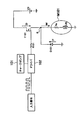
- FIG. 2 is a circuit diagram showing a load circuit including the power supply apparatus according to the second embodiment.
- the power supply apparatus shown in FIG. 2 is obtained by replacing the control unit for controlling on / off of the MOSFET (T2) from an analog circuit to a digital circuit.
- the control circuit 21a includes an inverter circuit 13 that inverts a PWM signal that is turned on and off at a predetermined duty ratio to generate an inverted signal, and outputs an output signal of the inverter circuit 13 for a predetermined time (for example, 10 [ ⁇ s]), and a one-shot multivibrator 15 that outputs an ON signal for a predetermined time (Tz) using the rise timing of the PWM signal output from the delay device 14 as a trigger. .
- the output signal of the one-shot multivibrator 15 is supplied to the gate of the MOSFET (T2).
- the output signal of the one-shot multivibrator 15 is a signal having an “H” level for a certain time Tz after the lapse of 10 [ ⁇ s] after the input signal supplied to the driver 12 is turned off. Output to the gate.
- the fixed time Tz is set to a time shorter than both the time Tx and the time Ty shown in FIG. Therefore, in a part of the period in which the electronic switch T1 is turned off, the MOSFET (T2) can be turned on and a reflux current can flow through the MOSFET (T2). If the return current IF still exists after the time (Tz + 10 [ ⁇ s]) has elapsed after the electronic switch T1 is turned off, this return current flows through the parasitic diode Dp. .
- control circuit 21a is configured by a digital circuit including the one-shot multivibrator 15, so in addition to the effects described in the first embodiment, It becomes possible to design a circuit by a simple method.
- the case of driving a radiator fan mounted on a vehicle has been described as an example.
- the present invention is not limited to this, and the motor load is controlled by PWM control using a DC power supply. It can be applied to the case of driving
Landscapes
- Engineering & Computer Science (AREA)
- Power Engineering (AREA)
- Control Of Direct Current Motors (AREA)
- Dc-Dc Converters (AREA)
- Electronic Switches (AREA)
Abstract
フライホイールダイオードの順方向電圧に起因して生じるエネルギー損失を低減することが可能な電力供給装置を提供する。直流電源VBとモータM1との間に設けられる電子スイッチT1をPWM制御してモータM1を駆動する負荷回路において、モータM1に対して並列にMOSFET(T2)を設ける。該MOSFET(T2)が有する寄生ダイオードDpは、負荷電流IDと逆向きとなる方向が順方向となるように設けられる。そして、電子スイッチT1がオフとされている期間の一部の期間にてMOSFET(T2)をオンとして、モータM1に流れる還流電流をMOSFET(T2)に流す。従って、フライホイールダイオードを用いる場合と対比してエネルギー損失を著しく低減することができる。
Description
本発明は、電子スイッチを所望のデューティ比でPWM制御することにより、モータ負荷に供給する電力を制御する電力供給装置に係り、特に、発熱によるエネルギー損失を低減する技術に関する。
従来より、直流電源と負荷の間にMOSFET等の電子スイッチを設け、該MOSFETをPWM制御して負荷に供給する電力を調整し、該負荷の出力を制御する負荷回路が多く用いられている(例えば、特許文献1参照)。
図4は、車両に搭載されるラジエータファン等に用いられるモータM101をPWM制御により駆動する負荷回路の構成を示す回路図であり、直流電源VB(例えば、車両に搭載されるバッテリ)のプラス端子とモータM101との間に、MOSFET等の電子スイッチT101が設けられている。なお、モータM101のインダクタンスをLM、電機子抵抗をRaとする。
電子スイッチT101のゲートは、抵抗R101を介してドライバ102に接続されている。また、ドライバ102には、チャージポンプ101が接続されている。そして、ドライバ102に所定の周期でオン、オフが繰り返される入力信号が供給されると、該ドライバ102より、チャージポンプ101の出力電圧が電子スイッチT101のゲートに出力され、電子スイッチT101が所定のデューティ比でPWM駆動される。
図4に示すように、電子スイッチT101に流れる電流をIDとし、モータM101に流れる電流をIMとすると、電子スイッチT101がオンとされ、直流電源VBのプラス端子→電子スイッチT101→モータM101→グランド→直流電源VBのマイナス端子、の経路で電流が流れる場合には、ID=IMである。このとき、モータM101のインダクタンスLMには、LM*IM2/2の電磁エネルギーが蓄積される。
また、電子スイッチT101がオフとされた場合には、電流IDはゼロとなるが、モータM101のインダクタンスLMにより、電流IMは流れ続けようとする。この電流をモータM101に還流させるために、モータM101に対して並列にフライホイールダイオードD101(以下、単に「ダイオード」という)が設けられている。電子スイッチT101とモータM101との接続点をa点とすると、ダイオードD101のカソードがa点に接続され、ダイオードD101のアノードがグランドに接続されている。
これにより、電子スイッチT101がオンとされているときにモータM101に流れていた電流IMは、電子スイッチT101がオフとされると、モータM101→グランド→ダイオードD101→a点→モータM101の経路で還流し、インダクタンスLMに蓄積された電磁エネルギーは、モータM101の駆動トルクに変換される。このとき、ダイオードD101に流れる電流を還流電流IFとすると、IF=IMとなる。
モータ電流IM(=IF)は、電機子抵抗Ra及びダイオードD101を流れることにより、電力損失を発生させる。
電機子抵抗Raにおける電力損失は、モータ駆動トルクの発生を伴うので、電子スイッチT101のオフ期間におけるモータM101の回転速度の低下を抑制する効果が有る。一方、ダイオードD101に発生する電力損失は、該ダイオードD101の順方向電圧降下をVFとすると、VF*IFで示される。この電力損失は熱に変換され、ダイオードD101の温度を上昇させるのみであり、モータM101の回転速度の維持には何等貢献しない。
モータM101のインダクタンスLMに蓄積された電磁エネルギーが電機子抵抗Ra及びダイオードD101の電力損失として消滅すると、a点の電圧はモータ電機子の慣性力による発電電圧まで上昇する。このとき、a点からグランドに向けて電流が流れるのをダイオードD101が阻止する。
即ち、インダクタンスLMに蓄積された電磁エネルギーの一部はモータM101のトルクに変換され、残りはダイオードD101の発熱となってしまう。従って、ダイオードD101における電力損失を低減することができれば、モータM101のトルクに変換する割合を増加させることができ、エネルギーの有効活用を図ることができ、且つ、ダイオードD101の発熱を低減できることになる。
上述したように、従来における負荷回路では、電子スイッチT101を用いてモータM101をPWM制御する場合に、電子スイッチT101がオンからオフに変化したときにインダクタンスLMに蓄積された電磁エネルギーにより生じる電流IMをフライホイールダイオードD101によりモータM101に還流させている。ところが、この方式を採用した場合にはフライホイールダイオードD101が発熱し、これに起因してエネルギー損失が発生するので、何とかこのエネルギー損失を低減したいという要望が高まっていた。
本発明は、このような従来の課題を解決するためになされたものであり、その目的とするところは、フライホイールダイオードの順方向電圧に起因して生じるエネルギー損失を低減することが可能な電力供給装置を提供することにある。
上記目的を達成するため、本発明によれば、直流電源(VB)とモータ負荷(M1)とを接続する配線上に設けられた電子スイッチ(T1)と、前記電子スイッチをPWM制御して前記モータ負荷を駆動する駆動部と、前記モータ負荷に流れる電流と逆向きとなる方向が前記寄生ダイオードの順方向となるように、前記モータ負荷に対して並列に配置された、寄生ダイオードを備える半導体素子(T2)と、前記PWM制御により前記電子スイッチがオフとなる期間の一部の期間にて、前記半導体素子をオンとする制御を行う制御部と、を備えた電力供給装置を提供する。
好適には、前記電子スイッチがオフとなった後再度オンとなるまでの間に、前記モータ負荷のインダクタンスに蓄積された電磁エネルギーが消滅する場合には、前記一部の期間を、前記電子スイッチがオフとなった後、該電子スイッチと前記モータ負荷とを接続する第1接続点(a点)の電圧がグランドレベル以下に低下した時刻から、前記電磁エネルギーの消滅により前記第1接続点の電圧が上昇を開始する以前の時刻までの間の期間とする。
好適には、前記半導体素子(T2)は、前記電子スイッチと前記モータ負荷とを接続する第1接続点に接続される第1の主電極、グランドに接続される第2の主電極、及び制御信号が入力される制御電極を備え、前記半導体素子は、前記制御電極にプラス電圧が印加された際にオンとなり、前記制御部は、前記電子スイッチがオンからオフに移行して前記第1接続点の電圧がグランドレベル以下に低下した際に、前記制御電極へのプラス電圧の印加を開始し、このプラス電圧を印加してから前記第1接続点の電圧が上昇を開始するまでの第1期間、または、プラス電圧を印加してから一定時間が経過するまでの第2期間のうちの、いずれか短い方の期間が経過した場合に、前記プラス電圧の印加を停止する。
好適には、前記半導体素子(T2)は、N型の電界効果トランジスタであり、前記第1の主電極はドレイン、前記第2の主電極はソース、前記制御電極はゲートであり、前記制御部は、前記直流電源とグランドとの間に配置される第1抵抗(R2)とトランジスタ(T3)との直列接続回路を有し、前記トランジスタ(T3)の制御入力端子は前記第1接続点に接続され、前記第1抵抗(R2)と前記トランジスタ(T3)とが接続される第2接続点(b点)は、コンデンサ(C1)と第2抵抗(R3)の直列接続回路を介してグランドに接続され、前記コンデンサ(C1)と前記第2抵抗(R3)とが接続される第3接続点(c点)は、前記半導体素子(T2)のゲートに接続される。
好適には、前記制御部は、前記PWM信号の反転信号を生成するインバータ回路と、前記インバータ回路の出力信号を所定時間遅延させる遅延回路と、前記遅延回路より出力されるPWM信号の立ち上がりのタイミングをトリガとして、一定時間のオン信号を出力する1ショットマルチバイブレータと、を備える。
本発明に係る電力供給装置では、モータ負荷(M1)に対して並列にMOSFET等の半導体素子(T2)を設けており、電子スイッチ(T1)をPWM制御してモータ負荷を駆動させる場合には、電子スイッチ(T1)がオフとなっている期間の一部の期間にて半導体素子(T2)をオンとする。従って、モータ負荷(M1)に流れる還流電流は半導体素子(T2)を経由して流れることになり、従来のフライホイールダイオードを用いる場合と対比して発熱を低減することができ、その結果、エネルギー損失を低減することができる。
以下、本発明の実施形態を図面を参照して説明する。図1は、本発明の第1実施形態に係る電力供給装置を含む負荷回路の構成を示す回路図である。図1に示すように、本実施形態に係る負荷回路は、例えば車両に搭載されるバッテリ等の直流電源VBと、MOSFET等の電子スイッチT1、及びラジエータファンの駆動用等に用いられるモータM1(モータ負荷)の直列接続回路を備えている。また、電子スイッチT1のゲートは抵抗R1を介してドライバ12に接続され、該ドライバ12はチャージポンプ11より電力が供給される。
そして、ドライバ12に所定周期でオン、オフが繰り返される入力信号が供給されると、ドライバ12より、チャージポンプ11の出力電圧が電子スイッチT1のゲートに出力され、電子スイッチT1が所定のデューティ比でPWM駆動される。その結果、モータM1に供給される電力が制御され、モータM1の回転駆動を制御することができる。ここで、モータM1が有する電機子抵抗をRa、インダクタンスをLMとする。
また、モータM1に対して並列に、N型のMOSFET(T2;半導体素子)が設けられている。該MOSFET(T2)のドレイン(第1の主電極)は、電子スイッチT1とモータM1の接続点であるa点(第1接続点)に接続され、ソース(第2の主電極)はグランドに接続されている。そして、該MOSFET(T2)が有する寄生ダイオードDpは、そのカソードがa点に接続され、そのアノードがグランドに接続されている。
MOSFET(T2)のゲート(制御電極)は、制御回路21に接続され、該制御回路21によりオン、オフが制御される。
制御回路21は、トランジスタT3(本実施形態ではMOSFETとしている)、抵抗R2(第1抵抗)、R3(第2抵抗)、コンデンサC1、及びダイオードD2を備えている。
抵抗R2の一端は直流電源VBのプラス端子に接続され、他端はトランジスタT3を介してグランドに接続されている。抵抗R2とトランジスタT3との接続点であるb点(第2接続点)は、コンデンサC1の一端に接続されている。また、トランジスタT3のゲートはa点に接続されている。
コンデンサC1の他端であるc点(第3接続点)は、MOSFET(T2)のゲートに接続され、且つ、抵抗R3を介してグランドに接続され、更に、ダイオードD2のカソードに接続されている。該ダイオードD2のアノードは、グランドに接続されている。
そして、制御回路21は、電子スイッチT1がオフとされている期間の一部の期間において、MOSFET(T2)をオンとすることにより、寄生ダイオードDpの発熱を低減し、その結果、エネルギー損失を低減する。
以下、第1実施形態に係る電力供給回路の動作について説明する。図3(a)-図3(e)は、第1実施形態に係る電力供給回路の各信号の波形を示すタイミングチャートであり、図3(a)はドライバ12に供給される入力信号の波形、図3(b)はa点、b点、c点に生じる電圧波形、図3(c)はモータM1に流れる電流IMの波形、図3(d)は電子スイッチT1に流れる電流IDの波形、そして図3(e)はMOSFET(T2)または寄生ダイオードDpに流れる還流電流IFを示している。
図1において、電子スイッチT1が駆動する前の状態では、a点の電圧は0Vであり、トランジスタT3はオフとなる。また、MOSFET(T2)のゲートは抵抗R3を介してグランドに接続されているので、該MOSFET(T2)はオフとなる。
いま、ドライバ12よりPWM信号が出力され、電子スイッチT1のゲートに駆動信号が供給されると、電子スイッチT1は所定のデューティ比でオン、オフを繰り返す。即ち、図3(a)に示すように、一定の周期で電子スイッチT1がオン、オフを繰り返す。図3(a)に示す時刻t1にて電子スイッチT1がオンとなると、図3(b)に示すように、a点の電圧はほぼ直流電源VBの出力電圧まで上昇する。また、図3(d)に示すように、電子スイッチT1に流れる電流IDは徐々に上昇する。同様に、図3(c)に示すように、モータM1に流れる電流IMは徐々に上昇する。
その結果、トランジスタT3のゲート電圧が上昇し、該トランジスタT3がオンとなり、b点がグランドに接続される。このため、MOSFET(T2)のゲートであるc点の電圧は、グランドレベルよりもダイオードD2の順方向電圧(これをVF2とする)だけ押し下げられた電圧となり、MOSFET(T2)はオフとなる。即ち、電子スイッチT1がオンとなる場合には、MOSFET(T2)はオフとなっている。
次いで、図3(a)に示す時刻t2にて電子スイッチT1がオフとなると、図3(b)に示すように、a点の電圧はグランドレベルを超えて急激に低下する。即ち、モータM1のインダクタンスLMに蓄積された電磁エネルギーにより、モータM1→グランド→寄生ダイオードDp→a点→モータM1の経路で還流電流が流れるので、a点の電圧が急激に低下する。このとき、図3(c)に示すように、モータM1に流れる電流IMは徐々に減少し、図3(e)に示すように、電流IMと同一の還流電流IFが寄生ダイオードDpに流れる。
そして、a点の電圧がグランドレベルよりも0.7V~1V程度低い電圧まで低下すると、a点の電位はMOSFET(T2)が有する寄生ダイオードDpによりクランプされ、それ以上の低下が制限される(図3(b)の符号q1参照)。つまり、寄生ダイオードDpがフライホイールダイオードとしての機能を果たすことになる。
そして、a点の電圧が低下することにより、トランジスタT3がオフとなり、b点とグランドとの接続が遮断されるのでb点の電圧が上昇する。b点電圧の上昇に追随して、c点電圧は、b点よりも0.7V程度低い電圧で上昇する(図3のt2~t3参照)。
c点電圧が上昇することにより、MOSFET(T2)がオンとなり、モータM1の還流電流IFは、寄生ダイオードDpをバイパスし、モータM1→グランド→MOSFET(T2)→a点→モータM1の経路で還流し、寄生ダイオードDpによる電力損失がMOSFET(T2)のオン抵抗による電力損失に置き換わる。一例として、MOSFET(T2)のオン抵抗が5[mΩ]、還流電流IFが10Aであるとすると、電力損失は0.5Wとなる。
これに対して、寄生ダイオードDpの順方向の電圧降下を0.7Vとすると、10Aの還流電流が流れた場合に7Wの電力損失となるので、MOSFET(T2)を用いることにより、電力損失が1/14となる。還流電流は電子スイッチT1がオフとなった時点で最大値となり、その後、一定勾配で減少するので、還流電流IFの2乗(IF2)に比例して電力損失も急激に減少する。
電子スイッチT1がオフとなった時刻t2から、時間Tyが経過した時刻t4(図3(b)参照)にて還流電流IFが消滅すると、電機子の慣性力による回転でモータM1が発電し、a点の電圧が上昇する(図3(b)の符号q2参照)。a点の電圧の上昇により、トランジスタT3がオンとなり、c点がグランドレベル以下となるので、MOSFET(T2)がオフとなる。これにより、a点→MOSFET(T2)→グランドの電流経路が遮断される。つまり、モータM1のインダクタンスLMに蓄積された電磁エネルギーが消滅した時点でMOSFET(T2)がオフとなるので、電機子の慣性エネルギーが浪費されることを防止できる。更に、電子スイッチT1が次にオンとなる時刻t5よりも前の時点で、確実にMOSFET(T2)をオフとすることができる。
また、電子スイッチT1がオフとなった直後に、c点の電圧はb点の上昇により引き上げられるが(図3のt2~t3参照)、直流電源VB→抵抗R2→コンデンサC1→抵抗R3→グランドの経路でコンデンサC1が充電されるので、c点の電圧は時間の経過に伴って低下する(図3のt3~t4参照)。このとき、コンデンサC1を充電する電流の時定数τは、τ=C1*(R2+R3)となり、この時定数τを小さく設定すれば還流電流が消滅してa点の電圧上昇が起こる前に、MOSFET(T2)をオフとすることができる。つまり、上記の時定数τを適宜変更することにより、電磁エネルギーが消滅する時点よりも前の時点で、MOSFET(T2)をオフとすることができる。
即ち、本実施形態では、電子スイッチT1がオンからオフに移行してa点の電圧がグランドレベル以下に低下した際に、MOSFET(T3)のゲートへのプラス電圧の印加を開始し、このプラス電圧を印加してからa点の電圧が上昇を開始するまでの期間(第1期間)、または、プラス電圧を印加してから時定数τで決定される一定時間が経過するまでの期間(第2期間)のうちの、いずれか短い方の期間が経過した場合に、プラス電圧の印加が停止してMOSFET(T2)がオフとなる。
MOSFET(T2)をオフとした後は、還流電流IFは寄生ダイオードDpを経由して流れることになる。この際、寄生ダイオードDpによる電力損失が懸念されるが、上記の時定数τで決定される時間の経過後には、還流電流IFが小さくなっているので、寄生ダイオードDpによる電力損失は極めて小さくなる。
このようにして、第1実施形態に係る電力供給装置では、モータM1に対して並列にMOSFET(T2)を設けている。そして、電子スイッチT1をPWM制御により駆動してモータM1に電力を供給する際に、電子スイッチT1がオフとされている期間の一部期間にてMOSFET(T2)をオンとしている。従って、電子スイッチT1がオフとされている際には、モータM1に流れる還流電流IFは、MOSFET(T2)を経由して還流するので、従来のようにフライホイールダイオードを経由して還流する場合と対比して、エネルギー損失を著しく低減することができる。
また、PWM制御実行時において、電子スイッチT1がオフとされた後に、MOSFET(T2)がオンとなり、電子スイッチT1がオンとなる前にMOSFET(T2)がオフとなるので、電子スイッチT1及びMOSFET(T2)の双方が同時にオンとなることを確実に回避できる。
なお、上述した第1実施形態では、還流電流が消滅するまでの経過時間Ty(図3(c)参照)が、電子スイッチT1のオフ時間Tx(図3(a)参照)よりも短くなるように設定したが、時間Txが時間Tyと等しいか、或いはTx<Tyとなっても、T1がオンとなることにより、a点の電位が上昇できれば制御は成立する。
そのためには、電子スイッチT1がオンとなるまでに、MOSFET(T2)のゲート電圧(c点の電圧)が十分に小さくなっていることが必要である。電子スイッチT1がオンとなったとき、MOSFET(T2)のゲート電圧が十分に大きいと、直流電源VB→電子スイッチT1→a点→MOSFET(T2)→グランドの経路で電流が流れ、負荷側配線が短絡接地したことと同一の現象となる。これを回避するためにも、コンデンサC1を充電してc点電位を低下させる制御が必要となる。
次に、本発明の第2実施形態について説明する。図2は、第2実施形態に係る電力供給装置を含む負荷回路を示す回路図である。図2に示す電力供給装置は、図1と対比して、MOSFET(T2)のオン、オフを制御するための制御部をアナログ回路からディジタル回路に置き換えたものである。
第2実施形態に係る制御回路21aは、所定のデューティ比でオン、オフ動作するPWM信号を反転して反転信号を生成するインバータ回路13と、該インバータ回路13の出力信号を所定時間(例えば、10[μs])遅延させる遅延器14と、該遅延器14より出力されるPWM信号の立ち上がりのタイミングをトリガとして、一定時間(Tz)のオン信号を出力する1ショットマルチバイブレータ15を備えている。そして、1ショットマルチバイブレータ15の出力信号は、MOSFET(T2)のゲートに供給される。
従って、1ショットマルチバイブレータ15の出力信号は、ドライバ12に供給される入力信号がオフとなってから、10[μs]経過した後に、一定時間Tzだけ「H」レベルの信号をMOSFET(T2)のゲートに出力する。
この際、一定時間Tzを、図3に示した時間Tx、及び時間Tyの双方よりも短い時間に設定する。従って、電子スイッチT1がオフとされている期間の一部の期間において、MOSFET(T2)をオンとし、MOSFET(T2)を経由して還流電流を流すことができる。また、電子スイッチT1がオフとなってから(Tz+10[μs])の時間が経過した後、未だ還流電流IFが存在する場合には、この還流電流は寄生ダイオードDpを経由して流れることになる。
このようにして、第2実施形態に係る電力供給装置では、1ショットマルチバイブレータ15を含むディジタル回路で制御回路21aを構成しているので、前述した第1実施形態に記載した効果に加え、より簡単な方法で回路を設計することが可能となる。
以上、本発明の電力供給装置を図示の実施形態に基づいて説明したが、本発明はこれに限定されるものではなく、各部の構成は、同様の機能を有する任意の構成のものに置き換えることができる。
例えば、上記した実施形態では、車両に搭載されるラジエータファンを駆動する場合を例に挙げて説明したが、本発明はこれに限定されるものではなく、直流電源を用いてPWM制御によりモータ負荷を駆動する場合について適用することができる。
本発明を詳細にまた特定の実施態様を参照して説明してきたが、本発明の精神、範囲または意図の範囲を逸脱することなく様々な変更や修正を加えることができることは当業者にとって明らかである。
本発明は、2008年12月25日出願の日本特許出願(特願2008-329693)に基づくものであり、その内容はここに参照として取り込まれる。
本発明は、2008年12月25日出願の日本特許出願(特願2008-329693)に基づくものであり、その内容はここに参照として取り込まれる。
PWM制御を用いてモータを駆動させる際に、エネルギー損失を低減する上で極めて有用である。
11 チャージポンプ
12 ドライバ
13 インバータ回路
14 遅延器
15 1ショットマルチバイブレータ
21,21a 制御回路(制御部)
VB 直流電源
T1 電子スイッチ
T2 MOSFET(半導体素子)
T3 トランジスタ
Dp 寄生ダイオード
D2 ダイオード
C1 コンデンサ
R1 抵抗
R2 抵抗(第1抵抗)
R3 抵抗(第2抵抗)
M1 モータ(モータ負荷)
Ra 電機子抵抗
LM インダクタンス
12 ドライバ
13 インバータ回路
14 遅延器
15 1ショットマルチバイブレータ
21,21a 制御回路(制御部)
VB 直流電源
T1 電子スイッチ
T2 MOSFET(半導体素子)
T3 トランジスタ
Dp 寄生ダイオード
D2 ダイオード
C1 コンデンサ
R1 抵抗
R2 抵抗(第1抵抗)
R3 抵抗(第2抵抗)
M1 モータ(モータ負荷)
Ra 電機子抵抗
LM インダクタンス
Claims (5)
- 電力供給装置であって、
直流電源とモータ負荷とを接続する配線上に設けられた電子スイッチと、
前記電子スイッチをPWM制御して前記モータ負荷を駆動する駆動部と、
前記モータ負荷に流れる電流と逆向きとなる方向が寄生ダイオードの順方向となるように、前記モータ負荷に対して並列に配置された、該寄生ダイオードを備える半導体素子と、
前記PWM制御により前記電子スイッチがオフとなる期間の一部の期間にて、前記半導体素子をオンとする制御を行う制御部と、
を備えたことを特徴とする電力供給装置。 - 前記電子スイッチがオフとなった後再度オンとなるまでの間に、前記モータ負荷のインダクタンスに蓄積された電磁エネルギーが消滅する場合には、前記一部の期間を、前記電子スイッチがオフとなった後、該電子スイッチと前記モータ負荷とを接続する第1接続点の電圧がグランドレベル以下に低下した時刻から、前記電磁エネルギーの消滅により前記第1接続点の電圧が上昇を開始する以前の時刻までの間の期間とする請求項1に記載の電力供給装置。
- 前記半導体素子は、前記電子スイッチと前記モータ負荷とを接続する第1接続点に接続される第1の主電極、グランドに接続される第2の主電極、及び制御信号が入力される制御電極を備え、
前記半導体素子は、前記制御電極にプラス電圧が印加された際にオンとなり、
前記制御部は、前記電子スイッチがオンからオフに移行して前記第1接続点の電圧がグランドレベル以下に低下した際に、前記制御電極へのプラス電圧の印加を開始し、このプラス電圧を印加してから前記第1接続点の電圧が上昇を開始するまでの第1期間、または、プラス電圧を印加してから一定時間が経過するまでの第2期間のうちの、いずれか短い方の期間が経過した場合に、前記プラス電圧の印加を停止する請求項1に記載の電力供給装置。 - 前記半導体素子は、N型の電界効果トランジスタであり、前記第1の主電極はドレイン、前記第2の主電極はソース、前記制御電極はゲートであり、
前記制御部は、前記直流電源とグランドとの間に配置される第1抵抗とトランジスタとの直列接続回路を有し、前記トランジスタの制御入力端子は前記第1接続点に接続され、前記第1抵抗と前記トランジスタとが接続される第2接続点は、コンデンサと第2抵抗の直列接続回路を介してグランドに接続され、前記コンデンサと前記第2抵抗とが接続される第3接続点は、前記半導体素子のゲートに接続される請求項1~請求項3のいずれか1項に記載の電力供給装置。 - 前記制御部は、
前記PWM信号の反転信号を生成するインバータ回路と、
前記インバータ回路の出力信号を所定時間遅延させる遅延回路と、
前記遅延回路より出力されるPWM信号の立ち上がりのタイミングをトリガとして、一定時間のオン信号を出力する1ショットマルチバイブレータと、
を備える請求項1に記載の電力供給装置。
Priority Applications (3)
| Application Number | Priority Date | Filing Date | Title |
|---|---|---|---|
| EP09834974.9A EP2372898B1 (en) | 2008-12-25 | 2009-12-24 | Power supply device |
| CN200980152850.0A CN102265501B (zh) | 2008-12-25 | 2009-12-24 | 供电装置 |
| US13/129,441 US8536819B2 (en) | 2008-12-25 | 2009-12-24 | Power supply device |
Applications Claiming Priority (2)
| Application Number | Priority Date | Filing Date | Title |
|---|---|---|---|
| JP2008329693A JP5303262B2 (ja) | 2008-12-25 | 2008-12-25 | 電力供給装置 |
| JP2008-329693 | 2008-12-25 |
Publications (1)
| Publication Number | Publication Date |
|---|---|
| WO2010074176A1 true WO2010074176A1 (ja) | 2010-07-01 |
Family
ID=42287783
Family Applications (1)
| Application Number | Title | Priority Date | Filing Date |
|---|---|---|---|
| PCT/JP2009/071491 Ceased WO2010074176A1 (ja) | 2008-12-25 | 2009-12-24 | 電力供給装置 |
Country Status (5)
| Country | Link |
|---|---|
| US (1) | US8536819B2 (ja) |
| EP (1) | EP2372898B1 (ja) |
| JP (1) | JP5303262B2 (ja) |
| CN (1) | CN102265501B (ja) |
| WO (1) | WO2010074176A1 (ja) |
Families Citing this family (9)
| Publication number | Priority date | Publication date | Assignee | Title |
|---|---|---|---|---|
| TW201225510A (en) * | 2010-12-07 | 2012-06-16 | xiang-yu Li | Safe motor energy recycling device |
| CN102570947A (zh) * | 2011-12-05 | 2012-07-11 | 江苏浩峰汽车附件有限公司 | 一种带制动功能的直流电机开关控制调速电路 |
| CN102739144B (zh) * | 2012-06-29 | 2015-07-22 | 深圳市航盛电子股份有限公司 | 一种微混合动力车用bsg电机控制系统 |
| CN104569857A (zh) * | 2015-01-21 | 2015-04-29 | 浪潮电子信息产业股份有限公司 | 一种替代负载仪的设计方法及其测试工具 |
| JP6671351B2 (ja) * | 2015-04-17 | 2020-03-25 | 日立オートモティブシステムズ株式会社 | 車載制御装置 |
| CN104953902B (zh) * | 2015-06-11 | 2018-06-19 | 南京普天大唐信息电子有限公司 | 一种开关磁阻电机功率控制电路 |
| US10868525B2 (en) * | 2018-11-13 | 2020-12-15 | Mohammad GH. Alijani | Power transmission through a single conductive element |
| JP7596736B2 (ja) | 2020-11-17 | 2024-12-10 | 株式会社オートネットワーク技術研究所 | 給電制御装置、給電制御方法及びコンピュータプログラム |
| FR3171133A1 (fr) * | 2025-01-08 | 2026-07-10 | Faurecia Sieges Dautomobile | Circuit électrique de commande d’un moteur électrique réversible et système de commande pour dispositif de verrouillage de glissière de siège de véhicule |
Citations (3)
| Publication number | Priority date | Publication date | Assignee | Title |
|---|---|---|---|---|
| JPS6489993A (en) * | 1987-09-29 | 1989-04-05 | Nippon Denso Co | Motor drive controller |
| JPH11168899A (ja) | 1997-12-01 | 1999-06-22 | Zexel:Kk | モータ駆動制御装置における駆動制御方法及びモータ駆動制御装置 |
| JP2000201475A (ja) * | 1999-01-04 | 2000-07-18 | Texas Instr Japan Ltd | 電源装置 |
Family Cites Families (5)
| Publication number | Priority date | Publication date | Assignee | Title |
|---|---|---|---|---|
| JP3626114B2 (ja) * | 2001-06-06 | 2005-03-02 | 株式会社デンソー | Dc−dcコンバータ |
| JP3494223B2 (ja) * | 2001-12-03 | 2004-02-09 | サンケン電気株式会社 | Dc−dcコンバ−タ |
| JP2005158870A (ja) | 2003-11-21 | 2005-06-16 | Fujitsu Ten Ltd | 負荷制御装置 |
| ATE410817T1 (de) * | 2005-06-01 | 2008-10-15 | Metabowerke Gmbh | Steuereinrichtung für einen gleichstromelektromotor eines elektrowerkzeuggeräts |
| JP2008099474A (ja) | 2006-10-13 | 2008-04-24 | Advics:Kk | 車両用電動モータ駆動回路 |
-
2008
- 2008-12-25 JP JP2008329693A patent/JP5303262B2/ja not_active Expired - Fee Related
-
2009
- 2009-12-24 EP EP09834974.9A patent/EP2372898B1/en active Active
- 2009-12-24 US US13/129,441 patent/US8536819B2/en not_active Expired - Fee Related
- 2009-12-24 WO PCT/JP2009/071491 patent/WO2010074176A1/ja not_active Ceased
- 2009-12-24 CN CN200980152850.0A patent/CN102265501B/zh not_active Expired - Fee Related
Patent Citations (3)
| Publication number | Priority date | Publication date | Assignee | Title |
|---|---|---|---|---|
| JPS6489993A (en) * | 1987-09-29 | 1989-04-05 | Nippon Denso Co | Motor drive controller |
| JPH11168899A (ja) | 1997-12-01 | 1999-06-22 | Zexel:Kk | モータ駆動制御装置における駆動制御方法及びモータ駆動制御装置 |
| JP2000201475A (ja) * | 1999-01-04 | 2000-07-18 | Texas Instr Japan Ltd | 電源装置 |
Also Published As
| Publication number | Publication date |
|---|---|
| CN102265501A (zh) | 2011-11-30 |
| EP2372898A4 (en) | 2017-11-22 |
| CN102265501B (zh) | 2014-08-20 |
| EP2372898B1 (en) | 2020-07-15 |
| JP5303262B2 (ja) | 2013-10-02 |
| US8536819B2 (en) | 2013-09-17 |
| EP2372898A1 (en) | 2011-10-05 |
| JP2010154647A (ja) | 2010-07-08 |
| US20110221376A1 (en) | 2011-09-15 |
Similar Documents
| Publication | Publication Date | Title |
|---|---|---|
| JP5303262B2 (ja) | 電力供給装置 | |
| JP6536466B2 (ja) | 電源装置 | |
| EP2418774B1 (en) | Semiconductor device driving unit and method | |
| CN106899208B (zh) | 电源系统 | |
| CN101946398B (zh) | 电机负载控制装置 | |
| CN104866000B (zh) | 具有稳压器的栅极驱动电路及方法 | |
| CN102906982B (zh) | 开关电源电路及其控制方法 | |
| KR101853600B1 (ko) | 충전 공용 인버터 | |
| JP5937455B2 (ja) | Led駆動回路 | |
| CN107306077B (zh) | 用于降低开关损耗的截止期间的igbt栅极驱动 | |
| CN108206644A (zh) | 电动汽车用的电源系统 | |
| JP2016208633A (ja) | モータ駆動装置 | |
| JP2017038513A (ja) | 半導体光源駆動装置 | |
| IT202300004365A1 (it) | Circuito di pilotaggio con controllo di scarica, sistema elettronico e veicolo corrispondenti | |
| CN112104204B (zh) | 用于控制功率转换器的开关器件的驱动的设备和方法 | |
| US20070127276A1 (en) | Power supply and display | |
| US7714523B2 (en) | Load driving method | |
| JP6767328B2 (ja) | ソレノイド駆動回路 | |
| JP4548484B2 (ja) | 同期整流型フォワードコンバータ | |
| JP2019118233A (ja) | Dc/dcコンバータの制御回路、制御方法、電源管理回路および電子機器 | |
| US6522557B2 (en) | Inverter device | |
| JP2008154431A (ja) | モータ制御装置 | |
| JP5465959B2 (ja) | 電動ファンの制御装置 | |
| CN107745655B (zh) | 一种电动车驱动电路的控制方法、控制单元和电动车 | |
| JP2007306681A (ja) | 昇圧回路および電動パワーステアリング装置 |
Legal Events
| Date | Code | Title | Description |
|---|---|---|---|
| WWE | Wipo information: entry into national phase |
Ref document number: 200980152850.0 Country of ref document: CN |
|
| 121 | Ep: the epo has been informed by wipo that ep was designated in this application |
Ref document number: 09834974 Country of ref document: EP Kind code of ref document: A1 |
|
| WWE | Wipo information: entry into national phase |
Ref document number: 13129441 Country of ref document: US |
|
| WWE | Wipo information: entry into national phase |
Ref document number: 2009834974 Country of ref document: EP |
|
| NENP | Non-entry into the national phase |
Ref country code: DE |