WO2010085000A1 - Imaging element and imaging apparatus using the same - Google Patents
Imaging element and imaging apparatus using the same Download PDFInfo
- Publication number
- WO2010085000A1 WO2010085000A1 PCT/JP2010/051314 JP2010051314W WO2010085000A1 WO 2010085000 A1 WO2010085000 A1 WO 2010085000A1 JP 2010051314 W JP2010051314 W JP 2010051314W WO 2010085000 A1 WO2010085000 A1 WO 2010085000A1
- Authority
- WO
- WIPO (PCT)
- Prior art keywords
- image
- light
- pixels
- imaging element
- pass filter
- Prior art date
- Legal status (The legal status is an assumption and is not a legal conclusion. Google has not performed a legal analysis and makes no representation as to the accuracy of the status listed.)
- Ceased
Links
Classifications
-
- G—PHYSICS
- G02—OPTICS
- G02B—OPTICAL ELEMENTS, SYSTEMS OR APPARATUS
- G02B5/00—Optical elements other than lenses
- G02B5/18—Diffraction gratings
- G02B5/1876—Diffractive Fresnel lenses; Zone plates; Kinoforms
- G02B5/188—Plurality of such optical elements formed in or on a supporting substrate
- G02B5/1885—Arranged as a periodic array
-
- H—ELECTRICITY
- H04—ELECTRIC COMMUNICATION TECHNIQUE
- H04N—PICTORIAL COMMUNICATION, e.g. TELEVISION
- H04N23/00—Cameras or camera modules comprising electronic image sensors; Control thereof
- H04N23/10—Cameras or camera modules comprising electronic image sensors; Control thereof for generating image signals from different wavelengths
- H04N23/12—Cameras or camera modules comprising electronic image sensors; Control thereof for generating image signals from different wavelengths with one sensor only
-
- H—ELECTRICITY
- H04—ELECTRIC COMMUNICATION TECHNIQUE
- H04N—PICTORIAL COMMUNICATION, e.g. TELEVISION
- H04N23/00—Cameras or camera modules comprising electronic image sensors; Control thereof
- H04N23/80—Camera processing pipelines; Components thereof
- H04N23/84—Camera processing pipelines; Components thereof for processing colour signals
-
- H—ELECTRICITY
- H04—ELECTRIC COMMUNICATION TECHNIQUE
- H04N—PICTORIAL COMMUNICATION, e.g. TELEVISION
- H04N23/00—Cameras or camera modules comprising electronic image sensors; Control thereof
- H04N23/70—Circuitry for compensating brightness variation in the scene
- H04N23/75—Circuitry for compensating brightness variation in the scene by influencing optical camera components
-
- H—ELECTRICITY
- H04—ELECTRIC COMMUNICATION TECHNIQUE
- H04N—PICTORIAL COMMUNICATION, e.g. TELEVISION
- H04N25/00—Circuitry of solid-state image sensors [SSIS]; Control thereof
- H04N25/10—Circuitry of solid-state image sensors [SSIS]; Control thereof for transforming different wavelengths into image signals
- H04N25/11—Arrangement of colour filter arrays [CFA]; Filter mosaics
- H04N25/13—Arrangement of colour filter arrays [CFA]; Filter mosaics characterised by the spectral characteristics of the filter elements
- H04N25/134—Arrangement of colour filter arrays [CFA]; Filter mosaics characterised by the spectral characteristics of the filter elements based on three different wavelength filter elements
-
- H—ELECTRICITY
- H10—SEMICONDUCTOR DEVICES; ELECTRIC SOLID-STATE DEVICES NOT OTHERWISE PROVIDED FOR
- H10F—INORGANIC SEMICONDUCTOR DEVICES SENSITIVE TO INFRARED RADIATION, LIGHT, ELECTROMAGNETIC RADIATION OF SHORTER WAVELENGTH OR CORPUSCULAR RADIATION
- H10F39/00—Integrated devices, or assemblies of multiple devices, comprising at least one element covered by group H10F30/00, e.g. radiation detectors comprising photodiode arrays
- H10F39/80—Constructional details of image sensors
- H10F39/805—Coatings
- H10F39/8053—Colour filters
-
- H—ELECTRICITY
- H10—SEMICONDUCTOR DEVICES; ELECTRIC SOLID-STATE DEVICES NOT OTHERWISE PROVIDED FOR
- H10F—INORGANIC SEMICONDUCTOR DEVICES SENSITIVE TO INFRARED RADIATION, LIGHT, ELECTROMAGNETIC RADIATION OF SHORTER WAVELENGTH OR CORPUSCULAR RADIATION
- H10F39/00—Integrated devices, or assemblies of multiple devices, comprising at least one element covered by group H10F30/00, e.g. radiation detectors comprising photodiode arrays
- H10F39/80—Constructional details of image sensors
- H10F39/806—Optical elements or arrangements associated with the image sensors
- H10F39/8067—Reflectors
Definitions
- the present invention relates to an imaging element which is used in an imaging apparatus such as a digital camera, or the like and an imaging apparatus having the same.
- an high sensitive imaging apparatus capable of obtaining a color image.
- multifunctional imaging apparatus capable of, for example, imaging a polarized image for detecting a wet state of a road surface with a high sensitivity has been required.
- the present invention is to provide an imaging element capable of achieving a normal color reproduction as well as high resolution and sensitivity can be achieved and ratio of pixels without filter can be increased, and an imaging apparatus using the imaging element.
- an imaging element includes a light receiving surface having pixels, a low-pass filter device configured to focus predetermined light on a predetermined pixel of the pixels of the light-receiving surface.
- FIG.l is a schematic configuration diagram of an imaging optical system having an imaging element according to an embodiment of the present invention.
- FIG.2A is a perspective view illustrating a low-pass filter viewed from a side of a lens.
- FIG.2B is a perspective view illustrating the low-pass filter viewed from a side of an imaging element body.
- FIG.2C is a sectional view illustrating the low-pass filter.
- FIG.3A is an explanatory view illustrating a case where light having wavelengths of 450 nm and 550 nm enters the low-pass filter on a diffracting surface of the low-pass filter at a side of a lens.
- FIG.3B is an explanatory view illustrating a case where light having wavelength of 650 nm enters the low-pass filter on the diffracting surface of the low-pass filter at the side of the lens.
- FIG.4 is a view illustrating a relationship between a 0-order light transmissivity or a first order light diffraction efficiency and a groove depth of concave -convex shapes on the diffracting surface of the low-pass filter at the side of the lens.
- FIG.5A is an explanatory view illustrating a case where the light having the wavelengths of 450 nm and 550 nm enters the low-pass filter on a diffracting surface of the low-pass filter at a side of an imaging element body.
- FIG.5B is an explanatory view illustrating a case where the light having the wavelength of 650 nm enters the low-pass filter on the diffracting surface of the low-pass filter at the side of the imaging element body.
- FIG.6 is a view illustrating a relationship between a 0-order light transmissivity or a first order light diffraction efficiency and a groove depth of concave -convex shapes on the diffracting surface of the low-pass filter at the side of the imaging element body.
- FIG.7 is an explanatory view explaining a structure of a filter array having a period of 6 X 6.
- FIG.8 is a view illustrating a flow to process an image imaged by an imaging element.
- FIG.9 is a view illustrating a flow to process an image imaged by an imaging element.
- FIG.10 is a view illustrating a flow to process an image imaged by an imaging element.
- FIG.11 is a view illustrating a flow to process an image imaged by an imaging element.
- FIG.12 is an explanatory view explaining a structure of a filter array having a period of 16 X 16 in a second embodiment.
- FIG.13 is a view illustrating paths of light beams when transmitting a birefringent medium.
- FIG.14A is a view illustrating a diffracting grating which a light beam enters.
- FIG.14B is a sectional view along B-B line of FIG.14A.
- FIG.14C is a view illustrating a transmitting state according to a polarization direction of a light beam.
- FIG.14D is a view illustrating a transmitting state according to a polarization direction of a light beam.
- FIG.15 is a sectional view illustrating a low-pass filter of the second embodiment.
- FIG.16 is a perspective view of the low-pass filter.
- FIG.17A is an explanatory view explaining a state where an extraordinary light beam enters the low-pass filter.
- FIG.17B is an explanatory view explaining a state where an ordinary light beam enters the low-pass filter.
- FIG.18 is a view illustrating a relationship between a 0-order light transmissivity or a first order light diffraction efficiency of the ordinary light beam and a groove depth of concave-convex shapes on the diffracting surface of the low-pass filter at the side of the imaging element body.
- FIG.19 is a sectional view illustrating a low-pass filter where diffracting structures are oppositely disposed.
- FIG.20 is a perspective view illustrating a low-pass filter having a periodic structure with a period smaller than a wavelength.
- FIG.21 is an explanatory view explaining a structure of a filter array having a period of 6 X 6 in a second embodiment.
- FIG.22 is a view illustrating a flow to process an image imaged by an imaging element.
- FIG.23 is a view illustrating a flow to process an image imaged by an imaging element.
- FIG.24 is a view illustrating a flow to process an image imaged by an imaging element.
- FIG.25 is a view illustrating a flow to process an image imaged by an imaging element.
- FIG.26A is a view illustrating an example of an image imaged by a vehicle camera.
- FIG.26B is an explanatory view explaining a method for processing an imaged result.
- An imaging element includes, as illustrated in FIG.l, a light receiving surface 15b having pixels, a low-pass filter device 14 such as a low-pass filter, a filter array having a lowpass filter (LPF) function or the like configured to focus predetermined light on a predetermined pixel or predetermined pixels of the pixels of the light-receiving surface 15b.
- the imaging element according to an embodiment of the present invention may be used in an imaging apparatus.
- the imaging apparatus may include a lens system 13 (ll), the imaging element configured to image a subject to form a subject image via the lens system, and a control device (not shown) configured to process the subject image as image data.
- FIG.l is a configuration diagram illustrating an imaging optical system including an imaging element according to an embodiment of the present invention.
- a left side of FIG.l indicates a subject side and a right side of FIG.l indicates an imaging plane side.
- Reference number 11 indicates a lens system 11 formed by one or more lenses
- reference number 12 indicates an aperture stop to set an F number within about 1 to 3
- reference number 13 indicates a lens system formed by one or more lenses
- reference number 15 indicates an imaging element body.
- the lens system 11 is disposed at the subject side from the aperture stop 12 and the lens system 13 is disposed at the imaging plane side from the aperture stop 12.
- the lens system 11, the aperture stop 12 and the lens system 13 are disposed on an optical axis L.
- the low-pass filter 14 and the imaging element body 15 are disposed in order from a side close to the lens system 13.
- the imaging element body 15 may be separately provided or integrally provided with the low-pass filter 14 [0014]
- Imaging element body 15 [Imaging element body 15]
- the imaging element body 15 a known monochrome sensor such as a CCD, a CMOS, or the like may be used.
- the imaging element body 15 is protected by a package 15c depending on an intended use and a lens-side surface of the package 15c is sealed by a cover glass 15a.
- a light-receiving part 15b as the light-receiving surface is provided at a center portion of the package 15c sealed by the cover glass 15a.
- the light-receiving part 15b may have pixels each having a size of predetermined micrometers, for example, about 1 to 9 micrometers, and the light-receiving part may have hundreds of thousands pixels or about 10 million, as recently used.
- a high thermally resistant package may be selected for using as a vehicle camera or an outdoor monitoring camera, and a small size package may be selected for using as a portable devices.
- the low-pass filter 14 may be configured to extract a wavelength component of the predetermined light when focusing the predetermined light on the predetermined pixel or predetermined pixels of the light-receiving surface 15b.
- the low-pass filter 14 is formed by a flat glass plate or a resin substrate having surfaces opposite each other, each surface being provided with diffracting structures.
- FIG.2A is a perspective view illustrating an end portion of the low-pass filter, viewed from a side of the lens systems.
- One end surface of the low-pass filter 14, which is disposed at the side close to the lens system 13, is divided into a plurality of areas 21a, 21b, ... .
- a concentric circular diffracting area 22a, 22b, ... is formed in each area 21a, 21b, ... .
- the diffracting area 22a is formed by a plurality of concentric circular bands about an optical axis 23a as a center
- the diffracting area 22b is formed by a plurality of concentric circular bands about an optical axis 23b as a center.
- a pitch (an interval) between the circular bands of a center part differs from that of a peripheral part to modulate the pitches between the circular bands. According to such a modulation, the diffracting areas 22a, 22b can have a lens function. Light-focusing capability becomes higher with decreasing the pitch or the interval between the circular bands. [0018]
- FIG.2B is a perspective view illustrating an end portion of the lowpass filter 14, viewed from a side of the imaging element body 15.
- the other end surface of the low-pass filter 14, which is disposed at a side close to the imaging element body 15, is divided into a plurality of areas 24a, 24b, ....
- the areas 24a, 24b, ... are disposed substantially at opposite positions of the areas 21a, 21b, ..., respectively. [0019]
- a concentric circular diffracting area 25a, 25b, ... is formed in each area 24a, 24b, ....
- the diffracting area 25a is provided with a plurality of concentric circular bands about an optical axis 26a as a center and the diffracting area 26a is provided with a plurality of concentric circular bands about an optical axis 26b as a center.
- FIG.2C is a sectional view illustrating a section of the low-pass filter 14, viewed in a direction shown by arrow A of FIG.2A.
- Sectional shapes of the diffracting structures are rectangular and the optical axes 23a, 26a of the diffracting areas are disposed so as to slightly deviate upwardly or downwardly from each other. Effective diameters of the diffracting areas 22a and 25a differ from each other and modulated degrees of the pitches and groove depths of the diffracting areas 22a and 25a are also different from each other.
- the shapes of the one end surface and the other end surface of the low-pass filter 14 differing from each other, light beams transmitting the areas 21a, 21b, ... and the areas 24a, 24b, ... are focused on different two point on the light-receiving surface 15b of the imaging element body 15, depending on the wavelengths of the light beams.
- the low-pass filter may be produced by forming a pattern in a die having a shape and performing an injection moulding or a so-called 2P method with a transparent material to copy a plurality of diffracting optical elements.
- the diffracting areas 22a, 22b, ... of the one end surface of the opposites surface of the low-pass filter 14, which is disposed at the side close to the lens system 13 have a function as a spatial low-pass filter for a light beam having a wavelength of 650 nm.
- the area 21a will be explained as a representative example.
- the diffracting area 22a formed in the area 21a is configured to emit a 0-order diffraction light when light having a wavelength of 450 nm or 550 nm enters the diffraction area 22a of the low-pass filter, that is, the diffracting area 22a is configured to transmit the light as a dead zone transmission and focus the transmitting light on a light-receiving area 31a as a part of the light-receiving part 15b of the imaging element body 15.
- the light-receiving area 31a corresponds to an area having 16 pixels.
- the one end surface of the low-pass filter 14 is configured to function as a mere transmitting element for the light having the wavelengths of 450 nm and 550 nm and function as a diffracting element for the light having the wavelength of 650 nm.
- the above-described wavelength selectivity can be achieved by selecting a groove depth of the diffracting structures.
- a periodic phase difference of concave -convex shapes in section of a diffracting grating to be 2n times (multiples of two) of a predetermined wavelength (for example, 450 nm, 550 nm) of a predetermined light which is desired to be selectively transmitted by the low-pass filter, a high 0-order light transmissivity can be achieved for the light having the wavelengths of 450 nm and 550 nm.
- FIG.4 is a view illustrating a relationship between the 0-order light transmissivity or the first order light diffraction efficiency of the diffracting grating having the sectional concave -convex shapes and the groove depth of the concave-convex shapes for the wavelengths of 450 nm, 550 nm, and 650 nm.
- Material for the used diffracting grating is quartz having a refractive index of 1.45.
- the 0-order light transmissivity for the wavelength of 450 nm and 550 nm is 90 % or more and the first order light diffraction efficiency for the wavelength of 650 nm is about 6 %.
- the light having the average (the light transmissivity of 6% per pixel for 16 pixels, that is, the light transmissivity of 96 %) of the wavelength of 650 nm, transmitting the area 21a is focused on the pixel 32a shown in FIG.3B.
- the light of 450 nm, 550 nm, and 650 nm are substantially uniformly received by the pixels of the light-receiving part 31a other than the pixel 32a.
- the other end surface of the low-pass filter 14, which is disposed at a side close to the imaging element body has the diffracting areas 25a, 25b, ....
- Each diffracting area 25a, 25b, ... functions as a spatial low-pass filter, mainly for the light having the wavelength 550 nm.
- the area 24a will be explained as a representative example.
- the diffracting area 25a formed in the area 24a is, as shown in FIG.5A, configured to emit substantially a 0-order diffraction light when the light having the wavelength of 450 nm and 650 nm enter the diffracting area 35a, that is, the diffracting area 25a transmits the light having the wavelengths of 450 nm and 650 nm as a dead zone transmission and focuses the transmitting light on the light-receiving area 31a of a part of the light-receiving part 15b of the imaging element body 15.
- the light-receiving area 31a corresponds to an area of 16 pixels.
- the low-pass filter 14 when the light having the wavelength of 550 nm enters the low-pass filter 14, as shown in FIG.5B, the first order diffraction light is focused on one pixel 32b on the light -receiving part 15b of the imaging element body. Accordingly, the other end of the low-pass filter 14 is configured to function as a mere transmitting element for the light having the wavelengths of 450 nm and 650 nm and function as a diffracting element for the light having the wavelength of 550 nm.
- the optical axis 26a of the diffracting area 25a is positioned so as to obliquely deviate by one pixel in a focused position from the optical axis 23a of the diffracting area 22a [0026] [Groove depth of the diffracting area 25a, or the like]
- the above-described wavelength selectivity can be achieved by selecting a groove depth of the diffracting structures.
- a periodic phase difference of concave -convex shapes in section of a diffracting grating to be 2n times (multiples of two) of a predetermined wavelength (for example, 450 nm, 650 nm) of a predetermined light, which is desired to be selectively transmitted by the low-pass filter, a high 0-order light transmissivity can be achieved for the light having the wavelengths of 450 nm and 650 nm.
- FIG.6 is a view illustrating a relationship between the 0-order light transmissivity or the first order light diffraction efficiency of the diffracting grating having the sectional concave -convex shapes and the groove depth of the concave-convex shapes for the wavelengths of 450 nm, 550 nm, and 650 nm.
- Material for the used diffracting grating is quartz having a refractive index of 1.45.
- the 0-order light transmissivity for the wavelength of 450 nm and 650 nm is 90 % or more and the first order light diffraction efficiency for the wavelength of 550 nm is about 7 %.
- the light having the average (the light transmissivity of 7% per pixel for 16 pixels, that is, the light transmissivity of about 100 %) of the wavelength of 550 nm, transmitting the area 25a is focused on the pixel 32b shown in FIG.5B.
- the light of 450 nm, 550 nm, and 650 nm are substantially uniformly received by the pixels of the light-receiving part 31a other than the pixel 32b.
- the light having the wavelength of 650 nm is focused on the pixel 32a on the light receiving area 31a of the imaging element body 15 and the light having the wavelength of 550 nm is focused on the pixel 32b.
- the light beams having the wavelengths 450 nm, 550 nm, and 650 nm uniformly enter the pixels other than the pixels 32a and 32b. Under such a receiving state, an color image can be formed from a monochrome image by the reconstruction processes described below with reference to, for example, FIGs. 8 to 11. [0029]
- the three wavelengths of 450 nm, 550 nm, and 650 nm are used but the wavelengths are not limited thereto.
- a combination of wavelengths of 470 nm, 520 nm, and 600 nm can be used.
- the combination of wavelengths can have further a near-infrared wavelength band, for example, about 850 nm in addition to the three wavelengths.
- Each area 21a, 21b, 24a, 24b and each diffracting area 22a, 22b, 25a, 25b may have a size variation (corresponding to a number of pixels) depending on a position thereof. That is, the sizes of the areas 21a, 21b, 24a, and 24b may be varied depending on the positions from a center of an optical axis of an imaging lens or the aperture stop to a peripheral area (an area out of the optical axis).
- the sectional shape of the diffracting grating may have a stepped structure.
- the diffraction order is not limited to the 0-order light and the first diffraction light and a second order light or a higher order light may be used.
- the optical axes 23a, 26a, 23b, and 26b of the diffracting areas of the front and rear side surfaces of the low-pass filter may be coaxial. In this case, the focusing positions of the diffracting areas 22a, 25a and the diffracting areas 22b, 25b are set to deviate from each other in a phase difference function.
- the diffracting structure may be formed on only one end surface.
- the wavelength selectivity can be achieved by use of a difference in the diffraction order, that is, it can be achieved, for example, when the light having the wavelength of 650 nm is focused on a pixel as a + first order light and the light having the wavelength of 550 nm is focused as a - first order light on a pixel different from the pixel where the + first order light is focused.
- the structure of the diffracting area is not limited to the concentric circular pattern and a liner pattern may be used.
- the diffraction light is focused on the imaging element body not as a point but a line and therefore, the image reconstruction can be achieved according to the liner pattern.
- the low-pass filter 14 is disposed separately from the imaging element body and between the lens system 13 and the imaging element body 15 is described, it is not limited thereto.
- the low-pass filter may be used as a substitute for the cover glass 15a of the imaging element body 15.
- the low-pass filter may be formed on a lens surface of the lens system 13.
- the low-pass filter may be formed integrally with the light-receiving part 15b. In this case, positional misalignment of the imaging element body or the like can be reduced to achieve a stable property.
- every array period of 6 X 6 has a pixel having a function of extracting a wavelength component of red light and a pixel having a function of extracting a wavelength component of blue light, which are disposed at a center of the array period.
- the pixel having the function of extracting the wavelength component of red light is referred to as the red filter
- the pixel having the function of extracting the wavelength component of blue light is referred to as the blue filter.
- color filter arrays are continuously disposed at a 6 X 6 pixel period.
- the pixels of the imaging element may be divided into a plurality of periods each having an anomalous pixel.
- the filter array may have an LPF characteristic such that a light amount of a light beam focused on the anomalous pixel configured to extract a predetermined wavelength component is larger than an average light amount of light beams of the predetermined wavelength component focused on pixels adjacent to the anomalous pixel entering within one period of the pixels of the imaging element.
- the pixels other than the pixels of the red and blue filters do not have a filter function but are configured to obtain brightness information and therefore are referred to as Y pixels hereinafter.
- the important point is that the R (red) pixel of the red filter and the B (blue) pixel of the blue filter have a spatial LPF effect. Therefore, an average value of an intensity of red light entering the array of the 6 X 6 and an average value of an average value of an intensity of blue light entering of the 6 X 6 can be obtained by the red pixel and the blue pixel, respectively.
- LPF low-pass filter
- the pixels having filter functions is provided with the spatial LPF effect and composing process is performed under the consideration of the spatial LPF effect so that the above-described problems can be solved.
- the process in this case is shown in FIG.8.
- the above-described control device may be configured to perform a separation process to separate the subject image formed by the imaging element into a first image formed by the predetermined pixels and a second image formed by the other pixels.
- the first image may be an image regarding color information and the second image may be an image regarding brightness information.
- the control device may be configured to perform an image expansion process to generate a fourth image by expanding the first image and an image composition process to compose the second and fourth images to form a third image in addition to the separation process.
- the control device may be configured to perform an image conversion process to convert color information of the second and third images into brightness information and to form a fifth image having brightness values of RGB in addition to the image expansion process and the image composition process.
- the control device may be configured to perform an image expansion process to expand the first image to form a fourth image, an LPF process to apply an LPF processing to the first image to form a sixth image by removing high frequency component from the first image, and an image composition process to compose the fourth and sixth images to form a third image in addition to the separation process.
- the control device may be configured to perform an image conversion process to convert color information of the second and third images into brightness information to form a fifth image having brightness values of RGB in addition to the image expansion process, the LPF process and the image composition process.
- the LPF process may be a process to average brightness values of pixels within a small range in relation to a period in which the predetermined pixels are arranged.
- the LPF process may include an image reduction process and an image expansion process.
- the third image may be an image relating to color information.
- a separation process is performed.
- signals from the imaging element are separated into a second image formed by Y pixels and a first image formed by R pixels and B pixels.
- failure parts in the second image formed by the Y pixels are interpolated by peripheral Y pixels before the following image composition process and the second image has a same size (a number of pixels) as the imaging element.
- an image expansion process is performed to expand the first image formed by the R pixels and B pixels such that the first image has a same size as the second image and then the image composition process is performed to generate Cb, Cr (color- difference) signals to form a third image.
- an image conversion process is performed to combine the second and third image and then generate a fifth image.
- the image conversion process for example, the following conversion equations are used.
- Cr_out 0.713 X (R_in - Y_in) where Y_in is input data of the second image, B_in and R_in are input signals of B pixels and R pixels of the fourth image, and Cb_out and Cr_out are output brightness signals and color signals of the third image.
- the Y (brightness) signals of the second image are combined and by use of signals of the imaging element, which are obtained from the above-described color filter array, a color image obtained from the YCbCr signals of the fifth image can be obtained.
- the process shown in FIG.9 may be performed so that high quality image with reduction of aliasing noise can be obtained.
- an LPF process to apply an LPF processing to the second image to obtain a sixth image is added. Since in this embodiment, the filter array of 6 X 6 is used, a filter smoothing 6 X 6 pixels is preferably used for the LPF processing. [0042]
- an image size of the reduced image is a same size as the size of the first image (that is, a pixel number of anomalous pixels of the imaging element) and an image size of the expanded image is a same size of the fourth image.
- FIG.11 is shown as a specific example of the processes shown in FIG.10.
- Table 1 (referred to as “Photo 1", hereinafter) shows an imaged image in the case where the color filter has the spatial LPF function and Table 2 (referred to as “Photo 2", herein after) shows an imaged image in the case where the color filter does not have the spatial LPF function. [0045] Table 1
- the color filters of R and B are used but other combinations of color filters, for example, of G and B, of R, G, and B, of IR (infrared) and B, and the like may be used.
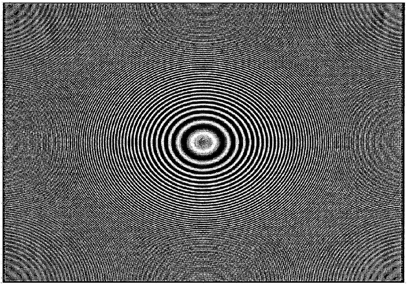
- Photo 4 is an input CZP image
- Photo 5 is an image imaged by using the imaging element according to this embodiment, that is, the imaging element having the color filter with the spatial LPF function
- Photo 6 is an image imaged by using the imaging element having the Bayer arrangement color filter. In Photo 5, generation of fake color is suppressed and high resolution can be achieved in comparison with Photo 6.
- the filter array of 6 X 6 is used to gather 1/36 of an R component of the pixel into the R pixel in the optical LPF, simply, white light has the R component of 1/3 of total light amount. That is, the brightness of the R pixel is 1/3 of the brightness of the Y pixel for a white subject. Accordingly, there is a problem in that S/N of the R pixels are degraded.
- the filter array is preferably configured such that each R component is set to have 3/36, that is, 1/12 to be gathered into the R pixels.
- the configuration for the B pixels is preferably the same.
- the low-pass filter may have a polarization-dependent characteristic changing depending on a polarization direction of the predetermined light.
- the polarization-dependent characteristic of the lowpass filter may be a characteristic to transmit only a predetermined polarization light component
- FIG.13 is a view illustrating paths of the light beams in a case where the light beams enter and transmit the general birefringent medium.
- a direction of the light beams is changed depending on polarizations of the light beams. That is, as shown in FIG.13, the light beam polarized in a direction parallel to a plane of FIG.13 in relation to the birefringent medium passes through the birefringent medium without change of the direction.
- the light beam is referred to as an ordinary light beam or a normal light beam.
- the light beam polarized in a direction perpendicular to the plane of FIG.13 in relation to the birefringent medium passes through the birefringent medium with changing the direction.
- the light beam is referred to as an extraordinary light beam or an anomalous light.
- FIG.14A is a view illustrating a surface of the diffracting grating, at a side where the light beam enters and
- FIG.14B is a sectional view along B-B line of FIG.14A.
- the diffracting grating shown in FIG.14B includes an isotropic medium 81, a birefringent medium 82, and glasses 83 disposed so as to sandwich the isotropic medium 81 and the birefringent medium therebetween.
- the birefringent medium 82 has a plurality of concentric circular bands (see FIG.14A), and each circular band has a rectangular shape in section. In the sectional view along B-B line of FIG.14A, the birefringent medium has concave-convex shapes.
- the isotropic medium 81 has complementary shapes in relation to the shapes of the birefringent medium and is in a contact state with surfaces of the concave -convex shapes of the birefringent medium 82.
- FIGs. 14C and 14D are views each illustrating a transmitting state of the light beams according to polarization directions of polarized light beams.
- the birefringent medium 82 has refractive indices of "no" and "ne” depending on the polarization directions of the light beams entering the birefringent medium.
- no is a refractive index (ordinary refractive index) for the ordinary light beam
- ne is a refractive index (extraordinary refractive index) for the extraordinary light beam.
- the polarization-selective diffracting grating is produced by selecting the isotropic medium 81 and the birefringent medium 82 so as to set a refractive index nl of the isotropic medium to be equal to ne will be explained.
- the refractive index of the isotropic medium 81 is the same as that of the birefringent medium so that the light beam can transmits without any influence.
- the refractive indices of the isotropic medium 81 and the birefringent medium are different from each other. Accordingly, the diffraction occurs due to the shapes of boundary surfaces of the isotropic medium and the birefringent medium 82 of the diffracting grating and the direction of the light beam is changed. As shown in FIGs.14C and 14D, the dead zone transmission or the light focusing is selected depending on the polarization of the entering light beam. [0070] [Low-pass filter 14]
- the low-pass filter 14 has the above -de scribed configuration and function of the polarization-selective diffracting grating. That is, the low-pass filter 14 has a sectional structure shown in FIG.15, in which diffracting structures 92 are formed on a glass plate or a resin substrate 91 by use of the birefringent medium. An isotropic medium 93 are complementarily added and the diffracting grating is sealed with a glass plate or a resin substrate 94. The light beam enters the sealing glass plate 94. [0071]
- FIG.16 is a perspective view illustrating an end portion of the low-pass filter 14, viewed from a side of the lens systems.
- the low-pass filter 14 is divided into a plurality of areas 101a, 101b, ... each having a same area.
- a concentric circular diffracting area 102a, 102b, ... is formed in each area 101a, 101b, ... .
- the diffracting area 102a is formed by a plurality of concentric circular bands about an optical axis 103a as a center
- the diffracting area 102b is formed by a plurality of concentric circular bands about an optical axis 103b as a center.
- a pitch (an interval) between the circular bands varies from a center part to a peripheral part to modulate the pitches between the circular bands. According to such a modulation, the diffracting areas can have a lens function. Light-focusing capability becomes higher with decreasing the pitch or the interval between the circular bands.
- the low-pass filter 14 As a method for producing the low-pass filter 14, a method applying a photolithographic technology or a method using precision cutting process with, for example, a diamond bite, may be used.
- the low-pass filter may be produced by forming a pattern in a die and performing an injection moulding or a so-called 2P method with a transparent material to copy a plurality of diffracting optical elements. [0074] [Diffracting area of the lowpass filter]
- the diffracting areas 102a, 102b, ... of the low-pass filter 14 have mainly a function as a spatial low-pass filter for a light beam having a polarization direction of an ordinary light.
- the area 101a will be explained as a representative example.
- the diffracting area 102a formed in the area 101a is configured to emit substantially a 0-order diffraction light when light having a polarization direction of the extraordinary light beam enters the diffraction area 102a of the low-pass filter, that is, the diffracting area 102a is configured to transmit the light as a dead zone transmission and focus the transmitting light on a light-receiving area Ilia as a part of the light-receiving part 15b of the imaging element body 15 (see FIG.l).
- the light-receiving area Ilia corresponds to an area having 16 pixels.
- the low-pass filter 14 is configured to function as a mere transmitting element for the extraordinary light beam and function as a diffracting element for the ordinary light beam.
- the above-described polarization-selectivity can be achieved by selecting a groove depth of the diffracting structures, the refractive index no of the ordinary light beam, the refractive index ne for the ordinary light beam, and the refractive index nl for the isotropic medium.
- FIG.18 is a view illustrating a relationship between the 0-order light transmissivity or the first order light diffraction efficiency for the ordinary light beam of the diffracting grating having sectional concave-convex shapes and the groove depth of the concave -convex shapes.
- the 0-order light transmissivity is 90 % or more and the first order light diffraction efficiency is about 7 %.
- the ordinary light beam is focused only on the pixel 112a of FIG.17B and the light having the average of the ordinary light passing through the area Ilia.
- the ordinary light beam and the extraordinary light beam are substantially uniformly received by the pixels of the light-receiving part 121a other than the pixel 112a.
- the light passing through the area 101a of the low-pass filter 14 is focused on the pixel 112a of the light-receiving area 11a of the imaging element body 15 as the ordinary light beam.
- the light of the extraordinary light beam is uniformly focused.
- the polarized image can be formed by using a monochrome imaging in the above-described reconstruction process with reference to FIGs.8 to 11.
- the diffraction structure may be formed at two sides. That is, as shown in FIG.19, in addition to the plate 91 where the diffraction structure 92 of the birefringent medium is formed, the low-pass filter may have a plate 91' where a diffraction structure 92' is formed at an opposite side of the plate 91 and an isotropic medium 93 is added therebetween. Furthermore, as described in the first embodiment, it is possible to set each diffracting surfaces such that a focusing position of each diffracting surface deviate from each other and the ordinary light beam and the extraordinary light beams are separately focused. [0079]
- Each area may have a size variation (corresponding to a number of pixels) depending on a position thereof. That is, the sizes of the areas 101a may be varied depending on the positions from a center of an optical axis of an imaging lens or the aperture stop to a peripheral area (an area out of the optical axis).
- the sectional shape of the diffracting grating may have a stepped structure.
- the diffraction order is not limited to the 0-order light and the first diffraction light and a second order light or a higher order light may be used.
- the structure of the diffracting area is not limited to the concentric circular pattern and a liner pattern may be used.
- the diffraction light is focused on the imaging element body not as a point but a line and therefore, the image reconstruction can be achieved according to the liner pattern.
- the lowpass filter 14 is disposed separately from the imaging element body 15 between the lens system 13 and the imaging element body 15 in this embodiment, it is not limited thereto.
- the lowpass filter may be used as a substitute for the cover glass 15a of the imaging element body 15.
- the polarization-selective diffracting grating is not limited to the combinations of the above-described isotropic material and birefringent material, and a diffracting grating using a sub-wavelength structure may be used. That is, as shown in FIG.20, the polarization selectivity can be achieved by superimposing the diffracting structure 92 having a pitch larger than the wavelength of the structure formed on the plate 91 with a periodic structure having a period ( ⁇ ) shorter than the wavelength.
- simple structure of the polarization selective diffracting grating can be achieved so that low cost and thin low-pass filter can be achieved.
- the first image may be an image regarding polarization information and the second image is an image regarding brightness information.
- a structure of a filter array of the imaging element will be explained. As shown in FIG.21, every array period of 6 X 6 has a pixel having a filter configured to transmit a P-polarized light and a pixel having a filter configured to transmit a S-polarized light at a center of the array period. Other pixels (referred to as Y pixels) have no filter function.
- the S-polarized filter and the P-polarized filter have also a spatial LPF effect and therefore, an average value of an intensity of the S-polarized light entering the array of the 6 X 6 and an average value of an intensity of the P-polarized light entering of the 6 X 6 pixels can be obtained.
- a remarkably large aliasing noise occurs in polarization information and therefore an information amount is largely decreased.
- an actual filter configured to transmit a polarized light and the above-described diffracting element, an SWS or the like may have a filter function.
- a separation process of anomalous pixels is performed.
- signals from the imaging element are separated into a second image formed by Y pixels and a first image formed by S-polarized pixels and P-polarized pixels.
- failure parts in the second image formed by the Y pixels are interpolated by peripheral Y pixels before the following image composition process and the second image has a same size (a number of pixels) as that of the imaging element (for example, 640 X 480, as shown in the above example).
- an image expansion process is performed to expand the first image formed by the S-polarized pixels and P-polarized pixels such that the first image has a same size as the second image and then the image composition process is performed to form a third image and therefore brightness information and corresponding polarization information constituting the third image can be obtained.
- the polarization information is not required to have same resolution as the brightness information, but the brightness information is required to have high resolution because the brightness information is used for displaying an image or performing a road surface detection processing.
- the method in this embodiment is preferable because the high resolution brightness information and the polarization information having low resolution but no occurrence of aliasing noise can be obtained by one imaging apparatus.
- the image composition process may include simply packing the brightness information and the polarization information having a same number of pixels each other and then passing the information to the following devices.
- the image composition process also may include assigning or providing the polarization information to the color difference information to display the color polarization information.
- FIG.23 shows an example where the first to third images are assigned or provided to the actual data.
- the case where the above-described filter array is used is more particularly shown in a process flow of FIG.24.
- the control device may be configured to perform an image reduction process to reduce the second image to form a fourth image and an image composition process to compose the first and fourth images to form a third image in addition to the separation process.
- a method shown in FIG.25 is also preferable. That is, at first, a separation process of anomalous pixels is performed. In the separation process, signals from the imaging element are separated into a second image formed by S-polarized pixels and a first image formed by P-pixels. At this time, failure parts in the second image formed by the Y pixels are interpolated by peripheral Y pixels before the following image composition process and the second image has a same size (a number of pixels) as the imaging element, for example, 640 X 480 pixels.
- an image reduction process is performed to reduce the second image of the brightness information such that the second image has a same size as the first image formed by the S-pixels and the P-pixels to form the fourth image.
- the image composition process is performed to generate a third image constituted by the brightness information and the corresponding polarization information from the fourth image and the first image.
- a color detection function to detect a color of a traffic light is necessary at an upper side of a screen and a function of detecting a wet road surface by using the polarization information is necessary at a lower side of the screen.
- an upper side of an imaging element is provided with the filter array of the first embodiment to obtain a color image and a lower side of the imaging element is formed by the configuration where the low-pass filter is configured to extract a wavelength component of the predetermined light when focusing the predetermined light, or other combinations of the different filter arrays to be used in each area.
- a low-pass filter configured to focus a predetermined light on a predetermined pixel on a light-receiving part of an imaging element
- high resolution and sensitivity of the imaging element can be achieved.
- ratio of pixels without filter can be increased as well as the imaging element capable of achieving a normal color reproduction can be provided.
Landscapes
- Signal Processing (AREA)
- Engineering & Computer Science (AREA)
- Multimedia (AREA)
- Physics & Mathematics (AREA)
- Optics & Photonics (AREA)
- General Physics & Mathematics (AREA)
- Spectroscopy & Molecular Physics (AREA)
- Studio Devices (AREA)
- Diffracting Gratings Or Hologram Optical Elements (AREA)
- Optical Filters (AREA)
- Polarising Elements (AREA)
- Solid State Image Pick-Up Elements (AREA)
- Color Television Image Signal Generators (AREA)
Abstract
Description




Claims
Priority Applications (4)
| Application Number | Priority Date | Filing Date | Title |
|---|---|---|---|
| CN201080005436.XA CN102318349B (en) | 2009-01-26 | 2010-01-26 | Imaging element and imaging apparatus using the same |
| US13/146,270 US8842211B2 (en) | 2009-01-26 | 2010-01-26 | Imaging element and imaging apparatus that extract light of a specific wavelength |
| EP10733601.8A EP2382787B1 (en) | 2009-01-26 | 2010-01-26 | Imaging element and imaging apparatus using the same |
| KR1020117017900A KR101265432B1 (en) | 2009-01-26 | 2010-01-26 | Imaging element and imaging apparatus using the same |
Applications Claiming Priority (2)
| Application Number | Priority Date | Filing Date | Title |
|---|---|---|---|
| JP2009-014195 | 2009-01-26 | ||
| JP2009014195A JP5572954B2 (en) | 2009-01-26 | 2009-01-26 | Image pickup device and image pickup apparatus including the image pickup device |
Publications (1)
| Publication Number | Publication Date |
|---|---|
| WO2010085000A1 true WO2010085000A1 (en) | 2010-07-29 |
Family
ID=42356045
Family Applications (1)
| Application Number | Title | Priority Date | Filing Date |
|---|---|---|---|
| PCT/JP2010/051314 Ceased WO2010085000A1 (en) | 2009-01-26 | 2010-01-26 | Imaging element and imaging apparatus using the same |
Country Status (7)
| Country | Link |
|---|---|
| US (1) | US8842211B2 (en) |
| EP (1) | EP2382787B1 (en) |
| JP (1) | JP5572954B2 (en) |
| KR (1) | KR101265432B1 (en) |
| CN (1) | CN102318349B (en) |
| TW (1) | TW201119361A (en) |
| WO (1) | WO2010085000A1 (en) |
Cited By (1)
| Publication number | Priority date | Publication date | Assignee | Title |
|---|---|---|---|---|
| WO2013189652A1 (en) * | 2012-06-20 | 2013-12-27 | Robert Bosch Gmbh | Detection of light for determining colour information |
Families Citing this family (13)
| Publication number | Priority date | Publication date | Assignee | Title |
|---|---|---|---|---|
| JP5713816B2 (en) | 2011-03-16 | 2015-05-07 | 株式会社東芝 | Solid-state imaging device and camera module |
| JP2013031054A (en) | 2011-07-29 | 2013-02-07 | Ricoh Co Ltd | Image pickup device and object detection device incorporating the same and optical filter and manufacturing method thereof |
| JP2013029451A (en) | 2011-07-29 | 2013-02-07 | Ricoh Co Ltd | Deposit detection device and deposit detection method |
| WO2013021554A1 (en) * | 2011-08-08 | 2013-02-14 | パナソニック株式会社 | Solid-state image pickup device |
| JP5853719B2 (en) * | 2012-01-20 | 2016-02-09 | 株式会社リコー | Image processing system and vehicle equipped with the same |
| JP5899957B2 (en) * | 2012-01-20 | 2016-04-06 | 株式会社リコー | Image processing system and vehicle equipped with the same |
| WO2014036660A1 (en) * | 2012-09-10 | 2014-03-13 | Bluelight Analytics Inc. | Devices and methods for measuring light |
| JP6417666B2 (en) * | 2013-05-15 | 2018-11-07 | 株式会社リコー | Image processing system |
| FR3007534A1 (en) | 2013-06-20 | 2014-12-26 | St Microelectronics Crolles 2 | PRODUCTION OF A NANOSTRUCTURE SPECTRAL FILTER |
| JP6380843B2 (en) | 2013-12-19 | 2018-08-29 | 株式会社リコー | Object detection apparatus, mobile device control system including the same, and object detection program |
| JP6676040B2 (en) * | 2015-04-08 | 2020-04-08 | マクセル株式会社 | Vehicle mounted camera |
| CN109716177B (en) * | 2016-09-15 | 2024-01-30 | 麦格纳国际公司 | Super surface lens assembly for chromaticity separation |
| EP3441804B1 (en) * | 2017-08-10 | 2024-09-11 | Canon Kabushiki Kaisha | Optical low-pass filter and imaging apparatus |
Citations (3)
| Publication number | Priority date | Publication date | Assignee | Title |
|---|---|---|---|---|
| JPH1118095A (en) * | 1997-06-20 | 1999-01-22 | Nikon Corp | Imaging device and recording medium |
| JP2005167356A (en) * | 2003-11-28 | 2005-06-23 | Canon Inc | Image sensor |
| JP2007109801A (en) * | 2005-10-12 | 2007-04-26 | Sumitomo Electric Ind Ltd | Solid-state imaging device and manufacturing method thereof |
Family Cites Families (20)
| Publication number | Priority date | Publication date | Assignee | Title |
|---|---|---|---|---|
| JP2696600B2 (en) | 1990-10-06 | 1998-01-14 | レオン自動機株式会社 | Envelope cutting device |
| JP2861525B2 (en) * | 1991-09-10 | 1999-02-24 | 松下電器産業株式会社 | Wavelength-selective phase grating optical low-pass filter |
| US6345116B1 (en) * | 1996-05-31 | 2002-02-05 | Matsushita Electric Industrial Co., Ltd. | Image processing apparatus |
| JP2000278503A (en) | 1999-03-23 | 2000-10-06 | Minolta Co Ltd | Device and method for bayer interpolation and recording medium recording bayer interpolation program |
| US6738510B2 (en) * | 2000-02-22 | 2004-05-18 | Olympus Optical Co., Ltd. | Image processing apparatus |
| JP2001235710A (en) * | 2000-02-24 | 2001-08-31 | Japan Science & Technology Corp | Diffractive optical element and imaging optical device |
| JP2004246644A (en) * | 2003-02-14 | 2004-09-02 | Pentax Corp | Image processing apparatus, image processing method, and image processing program |
| EP1678553A1 (en) * | 2003-10-23 | 2006-07-12 | Koninklijke Philips Electronics N.V. | Polarization independent phase modulator |
| WO2005101067A1 (en) * | 2004-04-13 | 2005-10-27 | Matsushita Electric Industrial Co., Ltd. | Condensing element and solid state imaging device |
| JP2005318465A (en) | 2004-04-30 | 2005-11-10 | Casio Comput Co Ltd | Imaging apparatus and image data processing method thereof |
| JP2006145814A (en) * | 2004-11-19 | 2006-06-08 | Pentax Corp | Digital camera |
| TWI351588B (en) | 2005-05-06 | 2011-11-01 | Seereal Technologies Gmbh | Device for holographic reconstructions of three-di |
| JP4974543B2 (en) | 2005-08-23 | 2012-07-11 | 株式会社フォトニックラティス | Polarization imaging device |
| US7978240B2 (en) * | 2005-10-03 | 2011-07-12 | Konica Minolta Photo Imaging, Inc. | Enhancing image quality imaging unit and image sensor |
| JP4144630B2 (en) | 2006-04-14 | 2008-09-03 | ソニー株式会社 | Imaging device |
| EP2012173A3 (en) * | 2007-07-03 | 2009-12-09 | JDS Uniphase Corporation | Non-etched flat polarization-selective diffractive optical elements |
| JP2009217123A (en) * | 2008-03-12 | 2009-09-24 | Fujinon Corp | Diffraction grating type low pass filter |
| JP4966894B2 (en) | 2008-03-18 | 2012-07-04 | 株式会社リコー | Imaging device |
| WO2009131925A2 (en) * | 2008-04-24 | 2009-10-29 | The Hong Kong University Of Science And Technology | Low voltage liquid crystal lens with a variable focal length |
| KR101544742B1 (en) * | 2008-12-08 | 2015-08-17 | 삼성전자주식회사 | Photographing apparatus and photographing method |
-
2009
- 2009-01-26 JP JP2009014195A patent/JP5572954B2/en active Active
-
2010
- 2010-01-26 CN CN201080005436.XA patent/CN102318349B/en not_active Expired - Fee Related
- 2010-01-26 WO PCT/JP2010/051314 patent/WO2010085000A1/en not_active Ceased
- 2010-01-26 TW TW099102143A patent/TW201119361A/en unknown
- 2010-01-26 KR KR1020117017900A patent/KR101265432B1/en active Active
- 2010-01-26 US US13/146,270 patent/US8842211B2/en active Active
- 2010-01-26 EP EP10733601.8A patent/EP2382787B1/en not_active Not-in-force
Patent Citations (3)
| Publication number | Priority date | Publication date | Assignee | Title |
|---|---|---|---|---|
| JPH1118095A (en) * | 1997-06-20 | 1999-01-22 | Nikon Corp | Imaging device and recording medium |
| JP2005167356A (en) * | 2003-11-28 | 2005-06-23 | Canon Inc | Image sensor |
| JP2007109801A (en) * | 2005-10-12 | 2007-04-26 | Sumitomo Electric Ind Ltd | Solid-state imaging device and manufacturing method thereof |
Non-Patent Citations (1)
| Title |
|---|
| See also references of EP2382787A4 * |
Cited By (2)
| Publication number | Priority date | Publication date | Assignee | Title |
|---|---|---|---|---|
| WO2013189652A1 (en) * | 2012-06-20 | 2013-12-27 | Robert Bosch Gmbh | Detection of light for determining colour information |
| US9521387B2 (en) | 2012-06-20 | 2016-12-13 | Robert Bosch Gmbh | Detection of light for ascertaining color information |
Also Published As
| Publication number | Publication date |
|---|---|
| EP2382787B1 (en) | 2016-11-23 |
| JP5572954B2 (en) | 2014-08-20 |
| KR20110112826A (en) | 2011-10-13 |
| EP2382787A1 (en) | 2011-11-02 |
| CN102318349B (en) | 2014-12-17 |
| JP2010171861A (en) | 2010-08-05 |
| KR101265432B1 (en) | 2013-05-16 |
| EP2382787A4 (en) | 2015-03-18 |
| TW201119361A (en) | 2011-06-01 |
| CN102318349A (en) | 2012-01-11 |
| US8842211B2 (en) | 2014-09-23 |
| US20110285898A1 (en) | 2011-11-24 |
Similar Documents
| Publication | Publication Date | Title |
|---|---|---|
| EP2382787B1 (en) | Imaging element and imaging apparatus using the same | |
| CN101779288B (en) | Solid-state imaging device | |
| CN103119516B (en) | Light field camera and image processing device | |
| JP5842146B2 (en) | Solid-state imaging device, imaging device, and spectroscopic element | |
| US9848118B2 (en) | Phase detection autofocus using opposing filter masks | |
| CN103503143B (en) | Solid-state imager and camera head | |
| US9425229B2 (en) | Solid-state imaging element, imaging device, and signal processing method including a dispersing element array and microlens array | |
| JP4527224B2 (en) | Solid-state imaging device including H-PDLC color separation element and manufacturing method thereof | |
| CN103004218A (en) | Three-dimensional imaging device, imaging element, light transmissive portion, and image processing device | |
| CN103503144B (en) | Solid-state imaging device | |
| JP5894573B2 (en) | Solid-state imaging device, imaging device, and signal processing method | |
| WO2013099151A1 (en) | Solid-state imaging element, imaging device, and signal processing method | |
| CN100437207C (en) | Color separator and imager | |
| JP4951209B2 (en) | Color separation device and imaging device | |
| JPH11295513A (en) | Device provided with color spectroscopic element | |
| JP2004139074A (en) | Color liquid crystal display and color filter |
Legal Events
| Date | Code | Title | Description |
|---|---|---|---|
| WWE | Wipo information: entry into national phase |
Ref document number: 201080005436.X Country of ref document: CN |
|
| 121 | Ep: the epo has been informed by wipo that ep was designated in this application |
Ref document number: 10733601 Country of ref document: EP Kind code of ref document: A1 |
|
| NENP | Non-entry into the national phase |
Ref country code: DE |
|
| WWE | Wipo information: entry into national phase |
Ref document number: 13146270 Country of ref document: US |
|
| REEP | Request for entry into the european phase |
Ref document number: 2010733601 Country of ref document: EP |
|
| WWE | Wipo information: entry into national phase |
Ref document number: 2010733601 Country of ref document: EP |
|
| ENP | Entry into the national phase |
Ref document number: 20117017900 Country of ref document: KR Kind code of ref document: A |