WO2010093012A1 - 受信装置、通信システム、受信方法及び通信方法 - Google Patents
受信装置、通信システム、受信方法及び通信方法 Download PDFInfo
- Publication number
- WO2010093012A1 WO2010093012A1 PCT/JP2010/052071 JP2010052071W WO2010093012A1 WO 2010093012 A1 WO2010093012 A1 WO 2010093012A1 JP 2010052071 W JP2010052071 W JP 2010052071W WO 2010093012 A1 WO2010093012 A1 WO 2010093012A1
- Authority
- WO
- WIPO (PCT)
- Prior art keywords
- signal
- unit
- phase
- real zero
- component
- Prior art date
- Legal status (The legal status is an assumption and is not a legal conclusion. Google has not performed a legal analysis and makes no representation as to the accuracy of the status listed.)
- Ceased
Links
Images


Classifications
-
- H—ELECTRICITY
- H04—ELECTRIC COMMUNICATION TECHNIQUE
- H04L—TRANSMISSION OF DIGITAL INFORMATION, e.g. TELEGRAPHIC COMMUNICATION
- H04L27/00—Modulated-carrier systems
- H04L27/32—Carrier systems characterised by combinations of two or more of the types covered by groups H04L27/02, H04L27/10, H04L27/18 or H04L27/26
- H04L27/34—Amplitude- and phase-modulated carrier systems, e.g. quadrature-amplitude modulated carrier systems
- H04L27/38—Demodulator circuits; Receiver circuits
- H04L27/3845—Demodulator circuits; Receiver circuits using non - coherent demodulation, i.e. not using a phase synchronous carrier
- H04L27/3854—Demodulator circuits; Receiver circuits using non - coherent demodulation, i.e. not using a phase synchronous carrier using a non - coherent carrier, including systems with baseband correction for phase or frequency offset
- H04L27/3863—Compensation for quadrature error in the received signal
-
- H—ELECTRICITY
- H04—ELECTRIC COMMUNICATION TECHNIQUE
- H04L—TRANSMISSION OF DIGITAL INFORMATION, e.g. TELEGRAPHIC COMMUNICATION
- H04L27/00—Modulated-carrier systems
- H04L27/0014—Carrier regulation
-
- H—ELECTRICITY
- H04—ELECTRIC COMMUNICATION TECHNIQUE
- H04L—TRANSMISSION OF DIGITAL INFORMATION, e.g. TELEGRAPHIC COMMUNICATION
- H04L27/00—Modulated-carrier systems
- H04L27/18—Phase-modulated carrier systems, i.e. using phase-shift keying
- H04L27/22—Demodulator circuits; Receiver circuits
- H04L27/233—Demodulator circuits; Receiver circuits using non-coherent demodulation
- H04L27/2335—Demodulator circuits; Receiver circuits using non-coherent demodulation using temporal properties of the received signal
- H04L27/2337—Demodulator circuits; Receiver circuits using non-coherent demodulation using temporal properties of the received signal using digital techniques to measure the time between zero-crossings
-
- H—ELECTRICITY
- H04—ELECTRIC COMMUNICATION TECHNIQUE
- H04L—TRANSMISSION OF DIGITAL INFORMATION, e.g. TELEGRAPHIC COMMUNICATION
- H04L27/00—Modulated-carrier systems
- H04L27/0014—Carrier regulation
- H04L2027/0024—Carrier regulation at the receiver end
- H04L2027/0026—Correction of carrier offset
Definitions
- the present invention relates to a reception device, a communication system, a reception method, and a communication method that receive a modulated wave that has been orthogonally modulated.
- IQ modulation signals obtained by orthogonally modulating (IQ modulation) such as PSK (Phase Shift Keying) and QAM (Quadrature Shift Amplitude Modulation), etc., from channel-coded bits.
- PSK Phase Shift Keying
- QAM Quadrature Shift Amplitude Modulation
- FIG. 25 is an example of a receiving apparatus that receives a signal subjected to quadrature modulation in single carrier transmission.
- the receiving device 900 includes a low noise amplification unit 902 (LNA: Low : Noise Amplifier), a frequency conversion unit 903, a filter unit 904, a gain control amplification unit 905, an IQ detection unit 906, an AD conversion unit 907, a demodulation unit Unit 908 and a decoding unit 909, to which an antenna unit 901 is connected.
- LNA Low noise amplification unit
- the orthogonally modulated signal received via the antenna unit 901 is amplified by the low noise amplifying unit 902 and then down-converted to a frequency band in which IQ detection can be performed by the frequency converting unit 903.
- the output signal of the frequency conversion unit 903 is processed by the gain control amplification unit 905 (AGC amplifier) after the harmonics and the out-of-band components are removed by the filter unit 904, and then the signal by the IQ detection unit 906 and the AD conversion unit 907. Is adjusted to an amplitude that is not clipped.
- the IQ detection unit 906 extracts an in-phase component (real number component) and a quadrature component (imaginary number component) from the output signal of the gain control amplification unit 905.
- each of the in-phase component signal and the quadrature component signal is converted from an analog signal to a digital signal.
- the demodulator 908 demaps the in-phase and quadrature component digital signals output from the AD converter 907 and calculates coded bits.
- the decoding unit 909 performs a decoding process on the encoded bits.
- the low noise amplification unit 902, the frequency conversion unit 903, the filter unit 904, the gain control amplification unit 905, and the IQ detection unit 906 are analog circuits, and the demodulation unit 908 and the decoding unit 909 are digital circuits.
- the AD conversion unit 907 performs conversion.
- the analog circuit of the receiving apparatus 900 described above in order to decode data with high accuracy, it is necessary to amplify the quadrature modulation wave, extract the in-phase / quadrature component, and process it linearly until it is input to the demapping process. There is. In other words, in order to reproduce the signal waveform with as little distortion as possible, an analog circuit having a high linearity and a wide dynamic range is required until it is input to the AD conversion unit 907. Further, the AD converter 907 needs to have a voltage resolution that satisfies a quantization error that can be absorbed by digital processing, and the gain control amplifier 905 has a wide range and high-accuracy gain control so that the AD converter 907 does not clip the signal. Is required.
- Non-Patent Document 1 is an example in which an analog circuit and a digital circuit are integrated to design an IC in a part having the same function, although the configuration order of each functional part is different from that of the receiving device 900.
- the present invention has been made in view of the above problems, and an object of the present invention is to provide a receiving device that enables decoding of a received signal with high accuracy even when sufficient linearity cannot be ensured in an analog circuit of the receiving device. Is to provide etc.
- the receiving device of the present invention is a receiving device that receives a modulated wave that has been orthogonally modulated, and adds a sine wave to the modulated wave to generate a real zero signal, and An in-phase / quadrature component detection unit that extracts an in-phase component signal and a quadrature component signal from the real zero signal; and a real zero sequence generation unit that generates a real zero sequence that is a sequence of times when the in-phase component signal and the quadrature component signal become zero. And a signal restoration unit for reproducing an in-phase component and a quadrature component from the real zero sequence.
- the real zero signal generation unit includes a time digital conversion unit that measures a time when the in-phase component signal and the quadrature component signal become zero.
- the in-phase / quadrature component detection unit includes an amplifying unit for limiting and amplifying the real zero signal.
- the in-phase / quadrature component detection unit includes an amplifying unit for limiting and amplifying the in-phase component signal and the quadrature component signal extracted from the real zero signal.
- the receiving apparatus of the present invention further includes a signal strength detection unit that detects the signal strength of the real zero signal, and the in-phase / quadrature component detection unit corrects in-phase component and quadrature component signals based on the signal strength. And a signal correction unit.
- the receiving apparatus of the present invention receives a multicarrier signal obtained by multicarrier modulation of the modulated wave, and the signal restoration unit restores each subcarrier signal of the multicarrier signal.
- a communication system is a communication system including a transmission device that transmits a modulated wave that is orthogonally modulated and a reception device that receives a modulated wave transmitted from the transmission device.
- An in-phase / quadrature component detection unit that extracts an in-phase component signal and a quadrature component signal from a real zero signal to which a sine wave is added, and a real zero that generates a real-zero sequence that is a sequence of times when the in-phase component and the quadrature component become zero.
- a sequence generation unit and a signal restoration unit that reproduces an in-phase component and a quadrature component from the real zero sequence are provided.
- the receiving device further includes a real zero signal generation unit that generates a real zero signal by adding a sine wave to the modulated wave.
- the transmitting device further includes a reference signal adding unit that adds a sine wave to the modulated wave, and the receiving device generates a real zero signal based on the sine wave. It further has a generating part.
- the receiving method of the present invention is a receiving method for receiving a quadrature-modulated modulated wave, adding a sine wave to the modulated wave to generate a real zero signal, and generating a real-zero signal from the real-zero signal.
- In-phase / quadrature component detection process for extracting a signal and a quadrature component signal
- a real-zero sequence generation process for generating a real-zero sequence that is a sequence of times when the in-phase component and the quadrature component become zero, an in-phase component from the real-zero sequence
- a signal restoration process for reproducing the orthogonal component.
- the communication method of the present invention is a communication method having a transmission process for transmitting a modulated wave that is orthogonally modulated and a reception process for receiving a modulated wave transmitted from the transmission device, wherein the reception process is performed on the modulated wave.
- a real zero signal generation process for adding a sine wave to generate a real zero signal
- an in-phase / quadrature component detection process for extracting an in-phase component signal and a quadrature component signal from the real zero signal
- the in-phase component and the quadrature component are zero.
- a real zero sequence generating process for generating a real zero sequence consisting of a predetermined time and a signal restoration process for reproducing an in-phase component and a quadrature component from the real zero sequence.
- the present invention even when sufficient linearity cannot be ensured in the analog circuit of the receiving apparatus and distortion occurs in the signal waveform, it is possible to suppress deterioration in decoding accuracy of the received signal.
- a quadrature modulated wave is received and a sine wave is added to the modulated wave to generate a real zero signal.
- an in-phase component signal and a quadrature component signal are extracted from the real zero signal, a real zero sequence that is a sequence of times at which the in-phase component and the quadrature component signal become zero is generated, and the in-phase component and the quadrature component are generated from the generated real zero sequence.
- the orthogonal component is reproduced.
- the time digital conversion unit that measures the time when the in-phase component signal and the quadrature component signal become zero, an analog signal can be obtained with high quantization accuracy even in an analog circuit operating at a low voltage. It can be converted into a digital signal, and power consumption can be reduced.
- signal amplification can be performed with a low-voltage analog circuit, and the power consumption of the receiving apparatus can be reduced.
- signal amplification is performed using a low-voltage circuit in a low frequency band such as a baseband by limiter amplification of an in-phase component signal and a quadrature component signal extracted from a real zero signal. Therefore, the amplification factor of the amplifying unit at a high frequency such as a carrier wave frequency can be reduced, and the power consumption of the receiving apparatus can be reduced.
- the signal intensity of the real zero signal can be detected, and the signals of the in-phase component and the quadrature component can be corrected based on the signal intensity. This makes it possible to reproduce the in-phase component and the quadrature component with high accuracy regardless of the received signal strength, the received signal bandwidth, and the frequency of the sine wave added when generating the real zero signal.
- a multicarrier signal obtained by multicarrier modulation of a modulated wave is received, and each subcarrier signal of the multicarrier signal is restored.
- PAPR Peak-to-Average-Power-Ratio
- the communication system uses a single carrier transmission method for signals that have been subjected to quadrature modulation (IQ modulation) such as PSK (Phase Shift Keying) and QAM (Quadrature Amplitude Modulation).
- IQ modulation quadrature modulation
- PSK Phase Shift Keying
- QAM Quadrature Amplitude Modulation
- FIG. 1 is a schematic block diagram illustrating the configuration of the transmission device 100 according to the first embodiment.
- the transmission apparatus 100 includes an encoding unit 102, a constellation mapping unit 103, a DA conversion unit 104, an orthogonal modulation unit 105, a band filter unit 106, a frequency conversion unit 107, a power amplification unit 108, and a first local A signal generation unit 109 and a second local signal generation unit 110 are provided, and the antenna unit 101 is connected.
- encoding section 102 performs error correction encoding on data bits that are digital signals input from an apparatus constituting an upper layer (not shown), and outputs the encoded bits to constellation mapping section 103. It is a functional part.
- the constellation mapping unit 103 is a functional unit that maps the encoded bits input from the encoding unit 102 to an in-phase component (real component, I) and a quadrature component (imaginary component, Q) based on the modulation multilevel number. is there.
- FIG. 2 shows an example of mapping when the coded bits are modulated by QPSK (modulation multilevel number: 2 bits). For example, when the encoded bit “00” is input from the encoding unit 102, the constellation mapping unit 103 outputs the in-phase component value i1 and the quadrature component value q1 according to the mapping rule of FIG.
- the DA conversion unit 104 is a functional unit that converts the in-phase component and the quadrature component output from the constellation mapping unit 103 from a digital signal to an analog signal and outputs the analog signal to the quadrature modulation unit 105.
- the quadrature modulation unit 105 performs quadrature modulation by multiplying the in-phase component and the quadrature component input from the DA conversion unit 104 by the carrier wave input from the first local signal generation unit 109, and the modulated wave is transmitted to the band filter unit 106. Output to. Specifically, the in-phase component value and the quadrature component value are multiplied by the sine wave of the center frequency fb1 generated by the first local signal generator 109, and the sine wave multiplied by the quadrature component value is multiplied by the in-phase component. Is shifted in phase by ⁇ / 2.
- the quadrature modulation unit 105 generates a modulated wave by adding a signal obtained by multiplying the in-phase component by a sine wave and a signal obtained by multiplying the quadrature component by a sine wave.
- This fb1 is also called an intermediate frequency (IF).
- the band filter unit 106 is a functional unit that removes out-of-band radiation from the modulated wave input from the quadrature modulation unit 105, extracts a modulated wave in a desired band including the center frequency, and outputs it to the frequency conversion unit 107.
- the frequency conversion unit 107 up-converts up to the transmission frequency band of the transmission apparatus 100 by multiplying the sine wave generated by the second local signal generation unit 110 by the modulation wave input from the band filter unit 106. Assuming that the carrier frequency of the transmission signal of the transmission apparatus 100 is fc, the frequency fb2 of the sine wave generated by the second local signal generation unit 110 is fc ⁇ fb1. This fc is also called a radio frequency (RF).
- the modulated wave output from the frequency conversion unit 107 is amplified by the power amplification unit 108 to the specification transmission power of the transmission apparatus 100 and transmitted via the antenna unit 101.
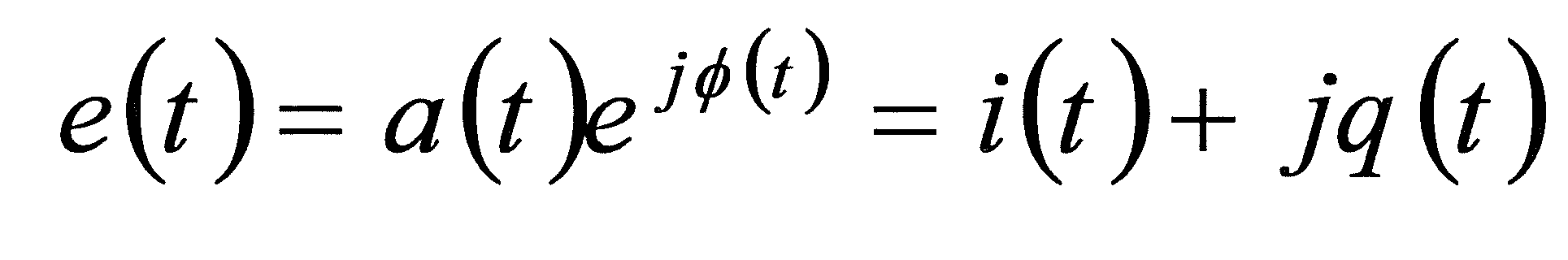
- a transmission signal s (t) of the transmission device 100 is expressed by the following expression (1).
- a (t) is the modulation amplitude
- ⁇ (t) is the modulation phase.
- the transmission signal s (t) is displayed by the complex envelope e (t), it can be expressed as the following expression (2).
- i (t) is an in-phase component value
- q (t) is a quadrature component value
- J is an imaginary unit
- R [x] is the real part of x.
- FIG. 3 is an example of the spectrum of the orthogonally modulated transmission signal s (t).
- the transmission signal s (t) is a modulated wave with a bandwidth of ⁇ fm centering on the carrier frequency fc.
- FIG. 4 is a schematic block diagram showing the configuration of the receiving apparatus 200 in the present embodiment.
- the receiving apparatus 200 includes a low noise amplification unit 202 (LNA: LowNANoise Amplifier), a band filter unit 203, a gain control amplification unit 204, a real zero signal generation unit 205 (reference signal addition unit), An in-phase / quadrature component detection unit 206, a real zero sequence generation unit 207, a signal restoration unit 208, a demodulation unit 209, and a decoding unit 210 are provided, and an antenna unit 201 is connected thereto.
- LNA Low noise amplification unit
- band filter unit 203 includes a band filter 203, a gain control amplification unit 204, a real zero signal generation unit 205 (reference signal addition unit),
- the low noise amplification unit 202 is a functional unit that amplifies the signal transmitted from the transmission device 100 received via the antenna unit 201 and outputs the amplified signal to the band filter unit 203.
- the band filter unit 203 is a functional unit that removes a signal outside the desired band from the signals input from the low noise amplification unit 202 and extracts a modulated wave in the desired band.
- the extracted modulated wave is output to the gain control amplification unit 204.
- the band filter unit 203 When receiving the transmission signal of the transmission apparatus 100, the band filter unit 203 has a pass bandwidth of 2 ⁇ fm, and extracts a band of fc ⁇ fm centering on the center frequency fc.
- the gain control amplification unit 204 amplifies the power of the modulated wave input from the band filter unit 203 to a level that can be processed by the real zero signal generation unit 205, and uses the signal power of the sine wave added by the real zero signal generation unit 205.
- the power of the signal input from the band filter unit is adjusted so as to be small (details will be described later). If the signal output from the gain control amplification unit 204 is r (t), the following equation (3) can be obtained.
- Ap is a total gain of a desired band from the low noise amplification unit 202 to the gain control amplification unit 204
- h (t) is a propagation path coefficient between the transmission side and the reception side.
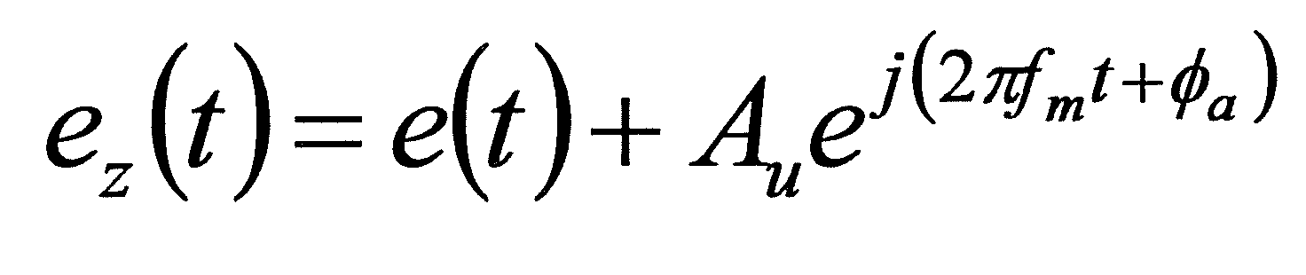
- the real zero signal generation unit 205 generates a real zero signal by adding a sine wave to the signal input from the gain control amplification unit 204.
- FIG. 5 is a schematic block diagram illustrating a configuration of the real zero signal generation unit 205.
- the real zero signal generation unit 205 includes an addition unit 221 and a reference signal generation unit 222.
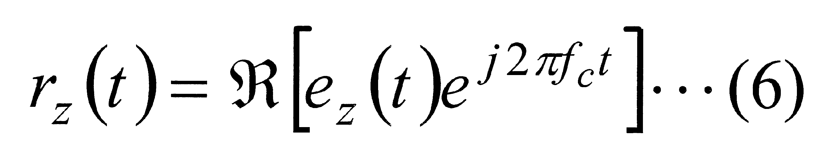
- the reference signal generator 222 generates a sine wave ra (t) having a frequency fa.
- the adder 221 generates a real zero signal rz (t) by adding a sine wave ra (t) to the received signal r (t) output from the gain control amplifier 204.
- the received signal r (t) is adjusted by the gain control amplification unit 204 so that the maximum value of the complex envelope becomes smaller than the amplitude of the sine wave ra (t).
- the gain control amplification unit 204 satisfies the following equation (4). To be adjusted.
- the frequency fa of the sine wave ra (t) is preferably outside the passband of the band filter unit 203. That is, when the pass band of the band filter unit 203 is 2 ⁇ fm, it is preferable to satisfy fa ⁇ fc ⁇ fm and fa> fc + fm. Further, the frequency fa of the sine wave ra (t) may be either fa ⁇ fc or fa> fc with respect to the carrier frequency fc of the reception signal r (t).
- FIG. 6 shows the spectrum of the real zero signal output from the adder 221 when fa ⁇ fc.
- the real zero signal rz (t) output from the adder 221 is expressed by the following equation (5).
- ⁇ a is the phase of the sine wave ra (t).
- FIG. 7 is a schematic block diagram showing another configuration of the real zero signal generator.
- the real zero signal generation unit 205-1 in FIG. 7 is different from the real zero signal generation unit 205 in FIG. 5 in that a gain control amplification unit 223 is provided.
- the gain control amplification unit 223 adjusts the amplitude Au of the sine wave input from the reference signal generation unit 222 based on the signal strength information of the received signal. Specifically, the amplitude Au is adjusted based on Ap ⁇ h (t) so as to satisfy the above-described formula (4).
- the gain control amplification unit 204 can be removed by setting the control that satisfies the above-described formula (4) only by the gain control amplification unit 223. As a result, the power consumption of the receiving apparatus can be reduced.
- the received signal strength information is measured by, for example, a propagation path estimation value calculated by propagation path estimation (not shown in the figure), RSSI (Received Signal Strength Indicator, not shown in the figure) provided in the receiving apparatus. Received signal strength etc.
- FIG. 8 is a schematic block diagram showing the configuration of the in-phase / quadrature component detection unit 206.
- the in-phase / quadrature component detection unit 206 includes an amplification unit 231, a band filter unit 232, multiplication units 233-1 and 233-2, low-pass filter units 234-1 and 234-2, a signal generation unit 235, A phase shift unit 236 and amplification units 237-1 and 237-2 are provided.
- the amplifying unit 231 is a functional unit for amplifying the real zero signal input from the real zero signal generating unit 205.
- FIG. 9 shows a change in the waveform in the complex plane when the real zero signal rz (t) is saturated and amplified.
- the dotted line indicates the locus of the in-phase / quadrature component when the real zero signal is saturated and amplified by limiter amplification.
- a black circle is a point where the in-phase component becomes 0 (zero) in the real zero signal.
- a white circle is a point where the orthogonal component becomes 0 in the real zero signal. That is, the real zero signal rz (t) forms a point (real zero) that becomes zero with respect to the in-phase component and the quadrature component.
- the in-phase component and the quadrature component of the quadrature-modulated modulated wave are detected using a time at which the in-phase component i (t) and the quadrature component q (t) of the real zero signal cross 0. . Therefore, if the time at which the in-phase component i (t) and the quadrature component q (t) of the real zero signal cross 0 is obtained accurately, the signal waveform may be distorted.
- the amplifying unit 231 may be an amplifying unit having a narrow linear region, and can reduce power consumption. Furthermore, the amplifying unit 231 can use a limiter amplifying unit that can perform a low voltage operation, and can further reduce the power consumption of the receiving apparatus 200.
- the band filter unit 232 removes unnecessary harmonics from the real zero signal input from the amplification unit 231 and outputs the result to the multiplication units 233-1 and 233-2.
- Multiplier 233-1 multiplies the real zero signal output from band filter unit 232 and the sine wave output from signal generator 235.
- the signal generator 235 down-converts the carrier frequency of the received signal and generates a sine wave having a frequency that can calculate the in-phase component and the quadrature component of the received signal.
- the receiving apparatus 200 of the present embodiment has a configuration using a zero IF (Low-IF), and the signal generator 235 generates a sine wave having a frequency fc.
- Multiplying unit 233-2 multiplies the real zero signal output from band filter unit 232 and the sine wave output from phase shift unit 236.
- the phase shifter 236 shifts the phase of the sine wave output from the signal generator 235 by ⁇ / 2.
- the low-pass filter unit 234-1 removes unnecessary harmonics from the signal input from the multiplier unit 233-1.
- the low-pass filter unit 234-2 removes unnecessary harmonics from the signal input from the multiplication unit 233-2.
- the in-phase component iz (t) and the quadrature component qz (t) output from the in-phase / quadrature component detection unit 206 output from the low-pass filter unit
- ⁇ a 0 is set for simplification.
- LPF [x] is the low-pass filter output of x.
- the amplifying unit 237-1 amplifies the in-phase component iz (t) output from the low-pass filter unit 234-1.
- the amplifying unit 237-2 amplifies the quadrature component qz (t) output from the low-pass filter unit 234-2.
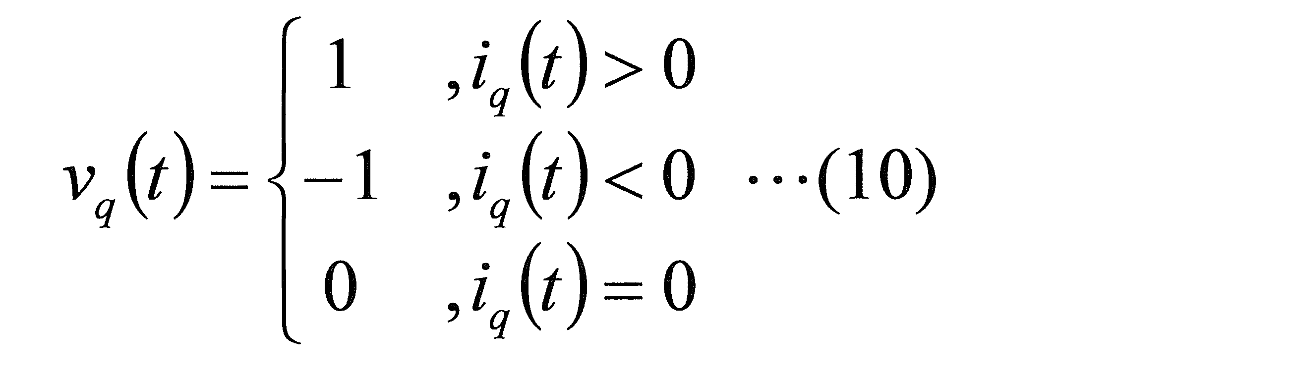
- the amplifying unit 237-1 and the amplifying unit 237-2 amplify to the signal amplitude that can calculate the real zero of the in-phase component and the quadrature component.
- the amplification unit 237-1 and amplification unit 237-2 preferably amplify the in-phase component iz (t) and the quadrature component qz (t) by saturation amplification. Since the amplification units 237-1 and 237-2 perform saturation amplification in a low frequency band (baseband band), the amplification factor of the amplification unit at a high frequency such as a carrier wave frequency can be lowered, so that the power consumption of the receiving apparatus is reduced. Electricity becomes possible.
- a signal vi (t) obtained by saturation amplification of the in-phase component iz (t) by the amplification unit 237-1 and a signal vq (t) obtained by saturation amplification of the quadrature component qz (t) by the amplification unit 237-2 are expressed by the following equations (9) ), (10).
- FIG. 10 is a schematic block diagram showing another configuration of the in-phase / quadrature component detection unit.
- the in-phase / quadrature component detection unit 206-1 includes an amplification unit 271, waveform shaping units 272-1 and 272-2, phase detection units 273-1 and 273-2, and low-pass filter units 234-1 and 234-. 2, a signal generation unit 274, a phase shift unit 236, and amplification units 237-1 and 237-2.
- the in-phase / quadrature component detection unit 206-1 includes the amplification unit 231, the band filter unit 232, the multiplication units 233-1 and 233-2, the signal generation unit 235, the in-phase / quadrature component detection unit 206 in FIG. Instead, an amplifier 271, waveform shapers 272-1 and 272-2, phase detectors 273-1 and 273-2, and a signal generator 274 are different. Hereinafter, different parts will be mainly described.
- the amplification unit 271 saturates and amplifies the real zero signal input from the real zero signal generation unit 205.
- the waveform shaping units 272-1 and 272-2 shape the signal input from the amplification unit 271 and generate a rectangular wave.
- an inverter circuit (NOT circuit) is used for the waveform shapers 272-1 and 272-2.
- the signal output from the waveform shaping units 272-1 and 272-2 is u ′ (t)
- the following equation (12) can be obtained.
- the output signals of the waveform shaping units 272-1 and 272-2 have a constant amplitude, and the value thereof is 1.
- the phase is maintained as ⁇ u (t).
- the rectangular function rect (x) has a period of 2 ⁇ .
- the phase detection unit 273-1 compares the phase of the signal input from the waveform shaping unit 272-1 with the phase of the signal output from the signal generation unit 274, and in-phase with the signal input from the waveform shaping unit 272-1.
- the component (I component) is extracted.
- the signal generator 274 generates a rectangular wave that becomes a reference signal in the phase detectors 273-1 and 273-2.
- the phase detection unit 273-2 compares the phase of the signal input from the waveform shaping unit 272-2 with the phase of the signal obtained by shifting the reference signal output from the signal generation unit 274 by ⁇ / 2 phase by the phase shift unit 236.
- the quadrature component (Q component) is extracted from the signal input from the waveform shaping unit 272-2.
- the phase detectors 273-1 and 273-2 have exclusive OR circuits (Exclusive OR circuits).
- the low-pass filter unit 234-1 removes unnecessary harmonics from the signal input from the phase detection unit 273-1, and outputs the result to the amplification unit 237-1.
- the low-pass filter unit 234-2 removes unnecessary harmonics from the signal input from the phase detection unit 273-2, and outputs the result to the amplification unit 237-2.
- tri (x) is a triangular function with a period of 2 ⁇ composed of positive and negative triangular waves of width ⁇ .
- the output signal v′i (t) of the low-pass filter unit 234-1 is saturated and amplified by the amplification unit 237-1, and the output signal vi (t) is expressed by the following equation (16).
- the output signal v′q (t) of the low-pass filter unit 234-2 is saturated and amplified by the amplification unit 237-2, and the output signal vq (t) is expressed by the following equation (17).
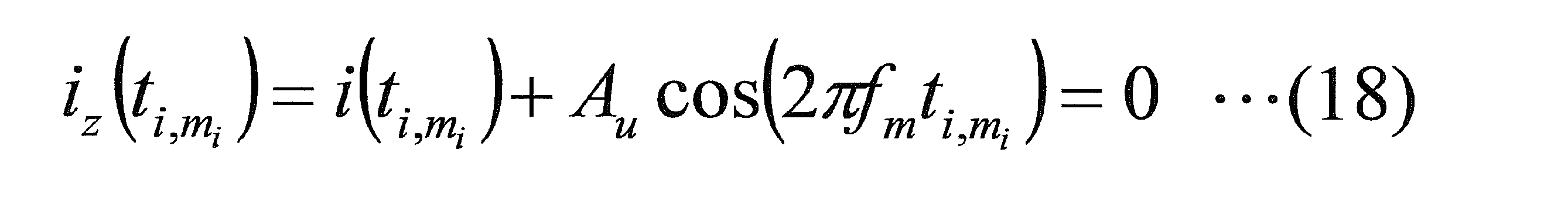
- the real zero sequence generation unit 207 crosses zero when the in-phase component signal vi (t) and the quadrature component signal vq (t) output from the in-phase / quadrature component detection unit 206 become zero.
- a time series zero crossing series is calculated.
- the time of a point indicated by a black circle where the in-phase component is 0 (zero) and a point indicated by a white circle where the orthogonal component is 0 are calculated. This operation corresponds to a function equivalent to a function of converting a signal from an analog signal to a digital signal in the prior art.
- the zero-cross sequence of the in-phase component vi (t) and the zero-cross sequence of the quadrature component vq (t) are sequences that satisfy the following expressions (18) and (19).
- the in-phase component vi (t) is a signal obtained by saturation amplification of iz (t)
- the quadrature component vq (t) is a signal obtained by saturation amplification of iq (t).
- the real zero sequence generation unit 207 outputs the in-phase component zero-cross sequence ⁇ i of the following equation (20) and the orthogonal component zero-cross sequence ⁇ q of the following equation (21).
- FIG. 11 is a schematic block diagram showing the configuration of the real zero sequence generation unit 207.
- the real zero sequence generation unit 207 includes a zero cross time calculation unit 241 (also referred to as a time digital conversion unit) and a clock generation unit 242.
- the zero-cross time calculation unit 241 uses the clock generated by the clock generation unit 242 to obtain the in-phase component and the quadrature component from the in-phase component vi (t) and the quadrature component vq (t) input from the in-phase / quadrature component detection unit 206. The time when it becomes zero is measured and the time is digitally output.
- FIG. 12 shows an operation in which the real zero sequence generation unit 207 measures a zero cross point.
- the signal of the in-phase component vi (t) or vq (t) is sampled by the clock (in FIG. 12, the rising point of the clock is the sampling point), and at the sampling point (the point indicated by the circle in FIG. 12)
- the zero cross point is calculated by estimating the time at which the signal of the in-phase component vi (t) or vq (t) changes from positive to negative (zero cross time, the time of the sampling point indicated by a black circle in FIG. 12). To do. For example, the zero cross time from the reference time is calculated.
- the clock generated by the clock generator 242 preferably has a high time resolution.
- a high time resolution clock having a picosecond order time resolution combining a digital control oscillator and a time digital converter can be applied.
- Such technologies include, for example, ⁇ Staszewski, et al. , Pp. 2278-2291, Dec. 2004 ”.
- FIG. 13 includes delay units 251-1 to 251 -N, flip-flop units 252-1 to 252 -N + 1, and a zero cross time determination unit 253.
- the delay units 251-1 to 251-N are connected in series to form a delay line.
- the delay units 251-1 to 251-N delay the input signal by ⁇ and then output it.
- inverters NOT circuits
- the flip-flop units 252-1 to 252-N + 1 are clock signals input from the clock generation unit 242 at the rising timing of the signal input from the in-phase / quadrature component detection unit 206, or some delay units of the clock signal. The value of the signal that passed through is output.
- D flip-flops can be applied as the flip-flop units 252-1 to 252-N + 1.
- the zero cross time determination unit 253 determines the time at which the signal input from the in-phase / quadrature component detection unit 206 changes from plus to minus from the signals output from the flip-flop units 252-1 to 252-N + 1.
- the clock generated by the clock generation unit 242 is input to the delay unit 251-1.
- the clock output from the delay unit 251-(N ⁇ 1) is input to the delay unit 251 -N.
- the clock output from the delay unit 251 -N is delayed by N ⁇ from the clock input to the delay unit 251-1.
- the clock output from (n ⁇ 1) is input.
- the flip-flop unit 252-n is a point at which the in-phase component vi (t) or the quadrature component vq (t) input from the in-phase / quadrature component detection unit 206 changes (a point at which the in-phase component changes from minus to plus, or from plus to minus.
- the clock input from the delay unit 251-(n ⁇ 1) is output.
- the zero cross time determination unit 253 determines how far the edge of the reference clock has advanced in the delay line by the delay units 251-1 to 251-N by the time when the in-phase component vi (t) or the quadrature component vq (t) changes. The zero crossing time is calculated by looking at the figure. Therefore, the zero cross time calculation unit 241 in FIG. 13 can estimate the zero cross time with the time resolution ⁇ .
- FIG. 14 is a schematic block diagram showing another configuration of the zero-crossing time calculation unit 241.
- the zero cross time calculation unit 241-1 includes an AD conversion unit 281, a low-pass filter unit 282, and a real zero time determination unit 283.
- the AD converter 281 converts the in-phase component vi (t) and the quadrature component vq (t) input from the in-phase / quadrature component detector 206 from an analog signal to a digital signal.
- the amplifying units 237-1 and 237-2 substantially store and amplify the zero-cross waveform of the analog waveform of the low-pass filters 234-1 and 234-2.
- the in-phase component vi (t) and the quadrature component vq (t) are signals in which the amplitude near level 0 is substantially linearly amplified, and the input range of the AD conversion unit 281 may be narrower than the AD conversion in the prior art. it can.
- the AD conversion unit 281 is for calculating the time at which the in-phase component vi (t) and the quadrature component vq (t) cross each other, and may be an AD conversion unit that is coarser than the AD conversion in the prior art. Therefore, the power consumption of the receiving device can be reduced.
- the low-pass filter unit 282 is a digital filter that linearly interpolates the in-phase component and the quadrature component discretized by the AD conversion unit 281 so as to be gentle.
- the real zero time determination unit 283 calculates the time when the in-phase component and the quadrature component become zero from the signal input from the low-pass filter unit 282.
- FIG. 15 shows a signal until the output signal of the AD conversion unit 281 is linearly interpolated by the low-pass filter unit 282 and a time series (real zero sequence) at which real zero is obtained is calculated.
- FIG. 15 shows an example when a signal having an in-phase component is input.
- the AD conversion unit 281 quantizes the in-phase component vi (t) input from the in-phase / quadrature component detection unit 206 according to the input clock, and outputs an in-phase component value indicated by a black circle in FIG.
- the low-pass filter unit 282 performs linear interpolation based on the in-phase component value, and outputs an in-phase component value indicated by a white circle in FIG. That is, the stepped waveform shown by the solid line in FIG. 15 is shaped into the waveform shown by the dotted line in FIG.
- the real zero time determination unit 283 outputs times ti0 and ti1 of in-phase component values close to zero (in-phase component values indicated by hatching in FIG. 15) among the in-phase component values indicated by white circles in FIG.
- the zero-cross time calculation unit 241-1 uses AD conversion with coarse accuracy, so that the clock generation unit 242 can calculate the zero-cross time with high accuracy even when a relatively low-speed clock such as a crystal oscillator is used. Is possible.
- FIG. 16 is a schematic block diagram showing the configuration of the signal restoration unit 208. As shown in FIG. 16, the signal restoration unit 208 includes a signal reproduction unit 261 and a low-pass filter unit 262.
- the low-pass filter unit 262 removes the sine wave component added for the real zero calculation from the in-phase component i ⁇ z (t) and the quadrature component q ⁇ z (t) output from the signal reproduction unit 261, and the phase of the transmission signal
- the component i (t) and the orthogonal component q (t) are extracted. That is, the component of the frequency fm is removed in the above formulas (15) and (16).
- the in-phase component i ⁇ z (t) and the quadrature component q ⁇ z (t) are Fourier transformed, and after removing the frequency fm, the inverse Fourier transform is performed. This can also be realized.
- the demodulator 209 demaps the in-phase and quadrature component digital signals output from the signal restoration unit 208 and calculates channel-coded data bits.
- the decoding unit 210 performs error decoding correction on the channel-encoded data bits and outputs data bits.
- the function of adjusting the power or amplitude of the signal is arranged in the previous stage of the real zero signal generation unit 205 (gain control amplification unit 204), but is arranged in the subsequent stage of the real zero signal generation unit 205. May be.
- this can be realized by providing the amplification unit 231 provided in the in-phase / quadrature component detection unit 206 with a gain control function for adjusting the power or amplitude of the signal. As a result, the degree of nonlinear distortion of the signal can be adjusted.
- the reference signal generator 222 included in the real zero signal generator 205 and the signal generator 235 included in the in-phase / quadrature component detector 206 perform signal generation separately.
- the two reference signals can be generated by multiplying the signal output from one signal generator serving as a reference for the two reference signal generators.
- the reference signal generator 222 and the signal generator 235 be an integer multiple of a predetermined common frequency.
- a PLL frequency synthesizer Phase Locked Loop
- a sine wave is added to the modulated wave as a reference signal.
- the present invention is not limited to this as long as a real zero sequence can be generated.
- the receiving device when a signal obtained by transmitting a quadrature-modulated signal using a single carrier transmission method is received, the receiving device adds a sine wave to the received signal.
- a real zero signal is generated, frequency conversion is performed using the generated real zero signal, in-phase / quadrature phase detection is performed, and then in-phase component and phase component are reproduced by time digital conversion. That is, the in-phase component and the phase component are reproduced using the time (real zero) when the in-phase component and the phase component become zero. Therefore, in the analog circuit of the receiving device, even when linearity cannot be maintained and waveform distortion occurs, deterioration of data decoding accuracy can be suppressed. Furthermore, in the communication system of the present embodiment, the analog circuit can be operated at a low voltage, so that power consumption can be kept low.
- the present invention can also be applied to a multicarrier transmission method such as OFDM (Orthogonal Frequency Domain Multiplexing). is there.
- OFDM Orthogonal Frequency Domain Multiplexing
- the output signal of signal restoration section 208 is subjected to FFT processing, and the in-phase component and the quadrature component of the subcarrier signal in which the modulated wave is arranged are extracted from the signal after the FFT processing, and demodulated. Input to the unit 209.
- the configuration using the zero IF (Low-IF) is described.
- the configuration is not limited to this, and the received signal such as a superheterodyne method is down-converted to an intermediate frequency (IF).
- IF intermediate frequency
- the present invention can also be applied to a method for detecting in-phase / quadrature components.
- the real zero signal generation unit 205 can be arranged in both RF and IF.
- the communication system described in the second embodiment is an embodiment in which a modified receiving device is applied from the communication system in the first embodiment.
- the transmission device in the second embodiment is the same as the transmission device 100 described in the first embodiment.
- FIG. 17 shows a schematic block diagram of the configuration of the receiving device 800 in the second embodiment.
- the receiving apparatus 800 includes a low noise amplification unit 202, a band filter unit 203, a gain control amplification unit 204, a real zero signal generation unit 205 (reference signal addition unit), a signal strength detection unit 801, An in-phase / quadrature component detection unit 806, a real zero sequence generation unit 207, a signal restoration unit 208, a demodulation unit 209, and a decoding unit 210 are provided, and an antenna unit 201 is connected thereto.
- the receiving apparatus 200 of the first embodiment is different from the receiving apparatus 200 in that it includes an in-phase / quadrature component detection unit 806 instead of the in-phase / quadrature component detection unit 206 and further includes a signal strength detection unit 801.
- an in-phase / quadrature component detection unit 806 instead of the in-phase / quadrature component detection unit 206 and further includes a signal strength detection unit 801.
- the signal strength detection unit 801 measures the signal strength value of the signal input from the real zero signal generation unit 205. The measured signal strength value is output to the in-phase / quadrature component detection unit 806.
- the in-phase / quadrature component detection unit 806 extracts an in-phase component (real component, I component) and a quadrature component (imaginary component, Q component) from the real zero signal rz (t) input from the real zero signal generation unit 205, and the in-phase component Further, the orthogonal component is corrected based on the received electric field strength of the real zero signal.
- FIG. 18 is a schematic block diagram showing the configuration of the in-phase / quadrature component detection unit 806.
- the in-phase / quadrature component detection unit 806 includes an amplification unit 231, a band filter unit 232, multiplication units 233-1 and 233-2, low-pass filter units 234-1 and 234-2, a signal generation unit 235, A phase shift unit 236, a weight control unit 822, and signal correction units 823-1 and 823-2 are provided.
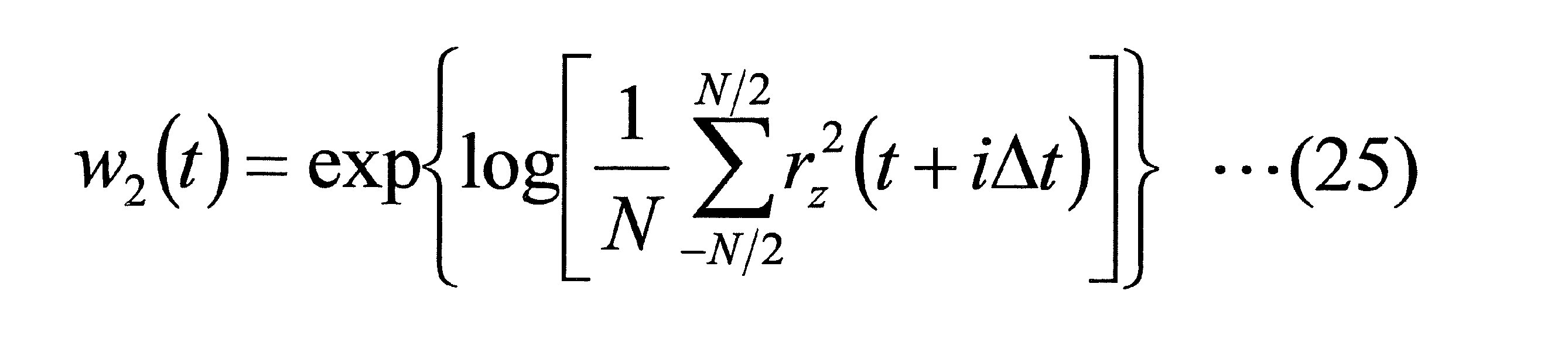
- the weight control unit 822 calculates a weighting factor based on the signal strength value output from the signal strength detection unit 801.
- the signal correction unit 823-1 corrects the in-phase component signal output from the multiplication unit 233-1 using the weighting factor.
- the signal correction unit 823-2 corrects the orthogonal component signal output from the multiplication unit 233-2 using the weighting factor.
- Equation (24) calculates an average value of a predetermined time TN of a signal obtained by amplifying the square detection value of the real zero signal rz (t) with a log amplifier, and uses an output value of an exponential function with respect to the average value as a power value. Is the case.
- Equation (25) is a case where a logarithmic value of a value obtained by averaging the square detection values of the real zero signal rz (t) at a predetermined time TN is calculated, and an output value of an exponential function with respect to the logarithmic value is used as a power value.
- square detection is used in Equations (24) and (25), it is also possible to calculate power using full-wave rectification detection.
- the weight control unit 822 calculates a weighting factor using the signal strength value input from the signal strength detection unit 801.
- the following equation (26) is an example of calculating a weighting coefficient from the signal intensity value of the equation (24) or the equation (25).
- the weight control unit 822 calculates a larger weight coefficient as the signal strength value increases.
- T N N ⁇ t (N is an arbitrary integer)
- the signal correction unit 823-1 corrects the signal by multiplying the in-phase component signal output from the multiplication unit 233-1 by the weighting factor.
- the signal correction unit 823-2 corrects the signal by multiplying the in-phase component signal output from the multiplication unit 233-2 by the weight coefficient.
- the in-phase or quadrature component signal corrected by the signal correction unit 823-1 or the signal correction unit 823-2 has unnecessary harmonics removed by the low-pass filter unit 234-1 or the low-pass filter unit 234-1. After that, it is output from the in-phase / quadrature component detection unit 806 and the real zero sequence generation unit 207 generates a real zero sequence.
- the in-phase component signal and the quadrature component signal extracted from the real zero signal are weighted based on the signal strength of the input real zero signal, thereby generating the phase component and quadrature generated by the real zero sequence generation unit 207. It is possible to improve the accuracy of the component zero-cross time series.
- the case where the signal correction based on the signal intensity is applied to the in-phase / quadrature component detection unit 206 using the multiplication type detection method has been described.
- the in-phase / quadrature component using the logical sum type detection method is described. It is also possible to apply to the detection unit 206-1.
- the communication system transmits a signal in which channel-coded data bits are subjected to quadrature modulation (IQ modulation) such as PSK (Phase Shift Keying) and QAM (Quadrature Amplitude Modulation) and a real zero reference signal.
- IQ modulation quadrature modulation
- PSK Phase Shift Keying
- QAM Quadrature Amplitude Modulation
- FIG. 19 is a schematic block diagram illustrating the configuration of the transmission device 500 according to the third embodiment.
- Transmitting apparatus 500 includes coding section 102, constellation mapping section 103, DA conversion section 104, orthogonal modulation section 105, reference signal addition section 501, band filter section 502, frequency conversion section 107, and power amplification.
- different parts will be mainly described.
- the reference signal adding unit 501 adds a sine wave to the modulation wave output from the quadrature modulation unit 105.
- the reference signal adding unit 501 has the same configuration as the real zero signal generating unit 205.
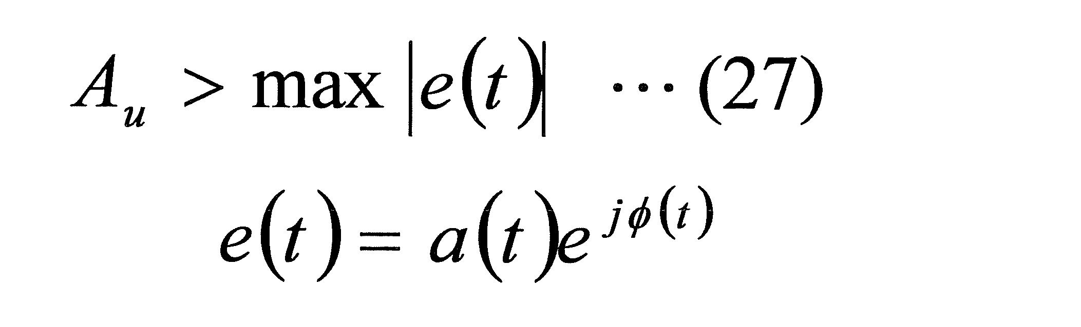
- the sine wave ra (t) (reference signal) added to the modulated wave output from the quadrature modulation unit 105 is desirably set to an amplitude Au that satisfies the following expression (27).
- e (t) is a complex envelope of the modulated wave output from the orthogonal modulation unit 105.
- the frequency fa of the sine wave ra (t) added to the modulation wave output from the quadrature modulation unit 105 is set to a frequency satisfying fa ⁇ fb1-fm, fa> fb1 + fm, (modulation wave bandwidth 2 ⁇ fm). To do.
- the band filter unit 502 removes out-of-band radiation from the signal output from the reference signal adding unit 501 and extracts a modulated wave and a sine wave ra (t) in a desired band including the center frequency.
- FIG. 20 shows a signal output from the band filter unit 502 when the sine wave ra (t) satisfying fa ⁇ fb1-fm is added by the reference signal adding unit 501.
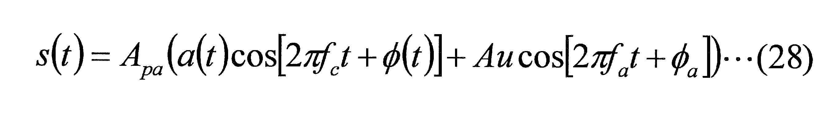
- the output signal of the band filter unit 502 is up-converted to the carrier frequency band fc by the frequency conversion unit 107 and amplified to the desired transmission signal power by the power amplification unit 108.
- a signal s (t) transmitted from the antenna unit 101 is expressed by the following equation (28). Apa is the total gain from the band filter unit to the power amplification unit.
- the reference signal is added to the modulated wave in the intermediate frequency band (IF band).
- the reference signal is obtained after up-converting the modulated wave to the carrier frequency band (radio frequency band, RF band).
- a signal may be added. This can be realized by configuring the reference signal adding unit 501 in the subsequent stage of the frequency converting unit 107 and setting the frequency fa of the reference signal to a frequency satisfying fa ⁇ fc ⁇ fm, fa> fc + fm.
- FIG. 21 is a schematic block diagram showing the configuration of the receiving device 600 in this embodiment.
- the receiving apparatus 600 includes a low noise amplification unit 202 (LNA: LowNANoise Amplifier), a band filter unit 203, a gain control amplification unit 204, a real zero signal generation unit 605, an in-phase / quadrature component detection unit 206.
- the receiving apparatus 600 is different from the receiving apparatus 200 in that a real zero signal generation unit 605 is provided instead of the real zero signal generation unit 205.
- the receiving device 600 receives a signal composed of a modulated wave and a reference signal (sinusoidal wave ra (t) added by the transmitting device) that are orthogonally modulated from the transmitting device 500, is amplified by the low noise amplifying unit 202, and is a band filter unit At 203, signals outside the desired band are removed.
- the band filter unit 203 has a pass band width through which the orthogonally modulated wave and the reference signal pass.
- the real zero signal generation unit 605 generates a real zero signal by adding a sine wave to the signal input from the gain control amplification unit 204.
- FIG. 22 is a schematic block diagram illustrating a configuration of the real zero signal generation unit 605.
- the real zero signal generation unit 605 includes an addition unit 221 and a reference signal reproduction unit 622.
- the reference signal reproduction unit 622 reproduces the reference signal by extracting and amplifying the reference signal from the modulated wave and the reference signal input from the gain control amplification unit 204. As the reference signal to be reproduced, an amplitude Au that satisfies the above equation (27) is set.
- the addition unit 221 adds the signal input from the gain control amplification unit 204 and the signal input from the reference signal reproduction unit 622. Thereby, even when the reference signal falls due to frequency selective fading of the propagation path, a real zero signal can be generated.
- the reference signal adding unit 501 of the transmission apparatus 500 can be set to reduce the amplitude level of the reference signal added, and the power loss of the transmission signal due to the addition of the reference signal can be suppressed. Note that when the signal received by the receiving apparatus 600 satisfies Expression (27), the real zero signal generation unit 605 can be omitted.
- the output signal of the band filter unit 203 is adjusted to a signal power that can be detected by the gain control amplification unit 204 and the in-phase / quadrature component detection unit 206, and then subjected to in-phase / quadrature component detection.
- the transmission apparatus transmits a signal (real zero signal) obtained by adding a sine wave serving as a real zero reference signal to a quadrature modulated wave.
- the receiving apparatus performs frequency conversion and in-phase / quadrature phase detection using the generated real zero signal, and then regenerates the in-phase component and the phase component using the time when the in-phase component and the phase component become zero (real zero). Therefore, in the analog circuits of the transmission device and the reception device, even when linearity cannot be maintained and waveform distortion occurs, deterioration in data decoding accuracy can be suppressed.
- the analog circuit can be operated at a low voltage, so that power consumption can be kept low.
- the communication system transmits a signal subjected to quadrature modulation (IQ modulation) such as PSK (Phase Shift Keying) and QAM (Quadrature Amplitude Modulation) using a multicarrier transmission method.
- IQ modulation quadrature modulation
- PSK Phase Shift Keying
- QAM Quadrature Amplitude Modulation
- a receiving device that receives a signal output from the transmitting device, and the receiving device reproduces in-phase and quadrature components using a real zero sequence.
- OFDM transmission method Orthogonal Frequency Domain Multiplexing
- FIG. 23 is a schematic block diagram illustrating a configuration of the transmission device 300 according to the fourth embodiment.
- Transmitting apparatus 300 includes coding section 102, constellation mapping section 103, IFFT section 301, DA conversion section 104, quadrature modulation section 105, band filter section 106, frequency conversion section 107, and power amplification section 108. And a first local signal generator 109 and a second local signal generator 110, to which the antenna unit 101 is connected.
- the transmission apparatus 300 is different from the transmission apparatus 100 of the first embodiment in that it includes an IFFT unit 301.
- different parts will be mainly described.
- the constellation mapping unit 103 converts the coded bits input from the coding unit 102 into in-phase components (real number component, I) based on the modulation multi-level number and the mapping rule of the modulation multi-level number (for example, FIG. 2). And the quadrature component (imaginary component, Q) are mapped, and the in-phase component value and the quadrature component value are output. Further, the constellation mapping unit 103 generates a number of OFDM modulated subcarriers for each of the in-phase component value and the quadrature component value, and outputs them to the IFFT unit 301.
- the IFFT unit 301 maps the in-phase component value and the quadrature component value input from the constellation mapping unit 103 to any one of several IFFT point inputs, and converts the signal from the frequency domain to the time domain by IFFT processing.
- Nsub ik + j ⁇ qk (j is an imaginary number) is mapped to the input of the IFFT unit and performs IFFT processing.
- the in-phase component signal and the quadrature component signal converted to the time domain are output.
- the output signal of the IFFT unit 301 is converted from a digital signal to an analog signal by the DA conversion unit 104, and then multiplied by the carrier wave input from the first local signal generation unit 109 by the quadrature modulation unit 105, thereby performing quadrature modulation. Do. Thereafter, the same processing as that of the transmission device 100 of the first embodiment is performed, and then transmitted via the antenna unit 101.
- the transmission signal s (t) of the transmission device 300 is expressed by the following expression (30).
- fk is the kth subcarrier frequency
- fc the carrier frequency
- Ts is the OFDM symbol period
- P the transmission power
- M Nsub / 2
- the complex envelope e (t) in the first embodiment is obtained by mapping a predetermined Ck calculated from the coded bits into one sine wave phase.
- Ck is set at equal frequency intervals. This is equivalent to mapping to multiple sine waves.
- FIG. 24 is a schematic block diagram showing a configuration of the receiving apparatus 400 in the present embodiment.
- the receiving device 400 receives the signal transmitted by the transmitting device 300, and performs a low noise amplification unit 202 (LNA: Low : Noise Amplifier), a band filter unit 203, a gain control amplification unit 204, and a real zero signal.
- a generation unit 205 reference signal addition unit
- the receiving device 400 is different from the receiving device 200 in that a signal restoring unit 408 is provided instead of the signal restoring unit 208.
- a signal restoring unit 408 is provided instead of the signal restoring unit 208.
- different parts will be mainly described.
- the receiving apparatus 400 receives the equation (30), and the real zero signal to which the sine wave is added in the real zero signal generation unit 205 (reference signal adding unit) can be expressed by the following equation (31).
- Expression (31) can be expressed as Expression (32).
- ⁇ f is a subcarrier frequency interval.
- the in-phase / quadrature component detection unit 206 extracts the in-phase component (real component, I component) and the quadrature component (imaginary component, Q component) from the equation (31), and the real-zero sequence generation unit 207 determines that the in-phase component and quadrature component are zero.
- the time (zero cross series) is calculated.
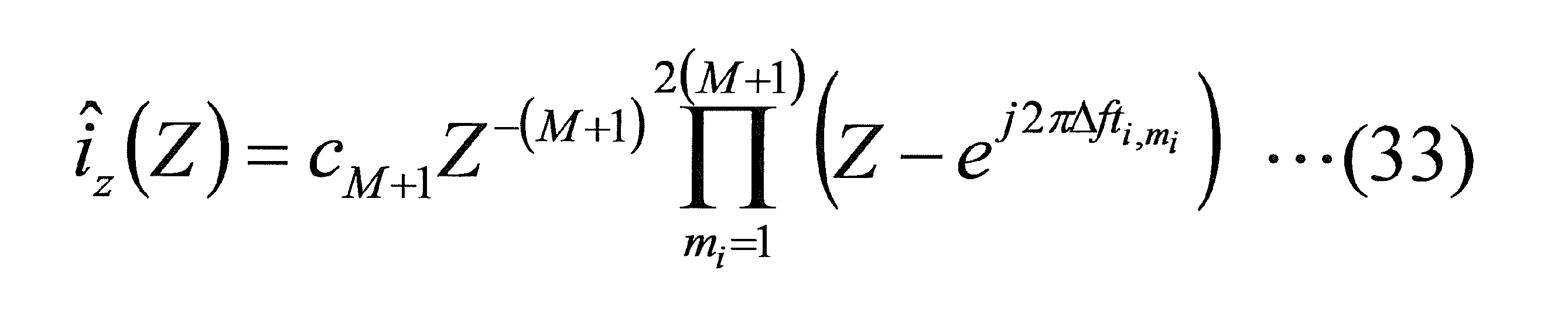
- the signal restoration unit 408 restores each subcarrier component of the OFDM-modulated signal from the in-phase component zero-cross sequence ⁇ i and the orthogonal component zero-cross sequence ⁇ q. Further, the signal restoration unit 208 extracts the in-phase component ik and the quadrature component qk from the in-phase component zero-cross sequence ⁇ i and the quadrature-component zero-cross sequence ⁇ q, and outputs them to the demodulation unit 209.
- equations (33) and (34) can be obtained.
- Equations (33) and (34) are subjected to FFT processing to extract the in-phase component ik and the quadrature component qk of each subcarrier.
- the in-phase component zero-cross sequence ⁇ i and the quadrature component input from the real zero sequence generation unit 207 Ck composed of the in-phase component ik and the quadrature component qk of the transmission signal is extracted by calculating a Fourier coefficient satisfying the Fourier series of the real zero signal from the zero-cross sequence ⁇ q.
- a Fourier coefficient lookup table for the real zero sequence is provided, and the Fourier coefficient is calculated by comparing the real zero sequence input from the real zero sequence generation unit 207 with the lookup table. calculate.
- a Fourier coefficient can be calculated from a real zero sequence by using a recursive algorithm based on Newton's formula.
- the receiving device when a signal in which an orthogonally modulated signal is transmitted using the OFDM method is received, the receiving device adds a sine wave to the received signal to generate a real zero signal. Generated, frequency converted using the generated real zero signal, in-phase / quadrature phase detection, and then time digital conversion to extract each subcarrier component of the OFDM-modulated signal and reproduce the in-phase component and phase component Do. Therefore, in the analog circuit of the receiving apparatus that receives an OFDM-modulated signal, even when linearity cannot be maintained and waveform distortion occurs, deterioration in data decoding accuracy can be suppressed. Furthermore, in the communication system of the present embodiment, the analog circuit can be operated at a low voltage, so that power consumption can be kept low.
- the present invention is not limited to this, but also in DFT-Spread-OFDM, MC-CDMA (Multi-Carrier--Code-Division-Multiple-Access), etc. It is possible to apply.
Landscapes
- Engineering & Computer Science (AREA)
- Computer Networks & Wireless Communication (AREA)
- Signal Processing (AREA)
- Digital Transmission Methods That Use Modulated Carrier Waves (AREA)
Abstract
Description
〔第1実施形態〕
第1実施形態における通信システムは、チャネル符号化された符号化ビットをPSK(Phase Shift Keying)、QAM(Quadrature Amplitude Modulation)などの直交変調(IQ変調)された信号をシングルキャリア伝送方式を用いて送信する送信装置と前記送信装置から出力される信号を受信する受信装置とを備え、前記受信装置は、リアルゼロ信号を用いて同相、直交成分を再生する。


つづいて、第2実施形態について説明する。第2実施形態に記載の通信システムは、第1実施形態における通信システムから、変形型の受信装置を適用した場合の実施形態である。ここで、第2実施形態における送信装置は、第1実施形態に記載の送信装置100と同様である。


つづいて、第3実施形態について説明する。第3実施形態における通信システムは、チャネル符号化されたデータビットをPSK(Phase Shift Keying)、QAM(Quadrature Amplitude Modulation)などの直交変調(IQ変調)された信号とリアルゼロの基準信号とを送信する送信装置と前記送信装置から出力される信号を受信する受信装置とを備え、前記受信装置は、リアルゼロ系列を用いて同相、直交成分を再生する。

つづいて、第4実施形態について説明する。第4実施形態における通信システムは、チャネル符号化されたデータビットをPSK(Phase Shift Keying)、QAM(Quadrature Amplitude Modulation)などの直交変調(IQ変調)された信号をマルチキャリア伝送方式を用いて送信する送信装置と前記送信装置から出力される信号を受信する受信装置とを備え、前記受信装置は、リアルゼロ系列を用いて同相、直交成分を再生する。以下では、マルチキャリア伝送方式として、OFDM伝送方式(Orthogonal Frequency Domain Multiplexing)を用いた場合で説明する。


101 アンテナ部
102 符号部
103 コンスタレーションマッピング部
104 DA変換部
105 直交変調部
106 帯域フィルタ部
107 周波数変換部
108 電力増幅部
109 第1ローカル信号発生部
110 第2ローカル信号発生部
200 受信装置
201 アンテナ部
202 低雑音増幅部
203 帯域フィルタ部
204 利得制御増幅部
205 リアルゼロ信号生成部
206 同相・直交成分検波部
207 リアルゼロ系列生成部
208 信号復元部
209 復調部
210 復号部
Claims (11)
- 直交変調された変調波を受信する受信装置であって、
前記変調波に正弦波を付加し、リアルゼロ信号を生成するリアルゼロ信号生成部と、
前記リアルゼロ信号から同相成分の信号及び直交成分の信号を抽出する同相・直交成分検波部と、
前記同相成分及び直交成分の信号がゼロとなる時刻の系列であるリアルゼロ系列を生成するリアルゼロ系列生成部と、
前記リアルゼロ系列から同相成分及び直交成分を再生する信号復元部と、
を備えることを特徴とする受信装置。 - 前記リアルゼロ信号生成部は、前記同相成分及び直交成分の信号がゼロとなる時刻を計測する時間ディジタル変換部を備えることを特徴とする請求項1に記載の受信装置。
- 前記同相・直交成分検波部は、前記リアルゼロ信号をリミッタ増幅する増幅部を備えることを特徴とする請求項1又は2に記載の受信装置。
- 前記同相・直交成分検波部は、前記リアルゼロ信号から抽出した同相成分の信号及び直交成分の信号をリミッタ増幅する増幅部を備えることを特徴とする請求項1から3の何れかに記載の受信装置。
- 前記リアルゼロ信号の信号強度を検出する信号強度検出部を更に備え、
前記同相・直交成分検波部は、前記信号強度に基づいて同相成分及び直交成分の信号を補正する信号補正部を備えることを特徴とする請求項1から4の何れかに記載の受信装置。 - 前記変調波をマルチキャリア変調したマルチキャリア信号を受信し、前記信号復元部は、マルチキャリア信号の各サブキャリア信号を復元することを特徴とする請求項1から5の何れかに記載の受信装置。
- 直交変調された変調波を送信する送信装置と前記送信装置から送信される変調波を受信する受信装置からなる通信システムであって、
前記受信装置は、
前記変調波に正弦波が付加されたリアルゼロ信号から同相成分の信号及び直交成分の信号を抽出する同相・直交成分検波部と、
前記同相成分及び直交成分がゼロとなる時刻の系列であるリアルゼロ系列を生成するリアルゼロ系列生成部と、
前記リアルゼロ系列から同相成分及び直交成分を再生する信号復元部と、
を備えることを特徴とする通信システム。 - 前記受信装置は、前記変調波に正弦波を付加し、リアルゼロ信号を生成するリアルゼロ信号生成部を更に備えることを特徴とする請求項7に記載の通信システム。
- 前記送信装置は、前記変調波に正弦波を付加する基準信号付加部を更に備え、
前記受信装置は、前記正弦波を基に、リアルゼロ信号を生成するリアルゼロ信号生成部を更に備えることを特徴とする請求項7に記載の通信システム。 - 直交変調された変調波を受信する受信方法であって、
前記変調波に正弦波を付加し、リアルゼロ信号を生成するリアルゼロ信号生成過程と、
前記リアルゼロ信号から同相成分の信号及び直交成分の信号を抽出する同相・直交成分検波過程と、
前記同相成分及び直交成分がゼロとなる時刻の系列であるリアルゼロ系列を生成するリアルゼロ系列生成過程と、
前記リアルゼロ系列から同相成分及び直交成分を再生する信号復元過程と、
を備えることを特徴とする受信方法。 - 直交変調された変調波を送信する送信過程と前記送信装置から送信される変調波を受信する受信過程を有する通信方法であって、
前記受信過程は、
前記変調波に正弦波を付加し、リアルゼロ信号を生成するリアルゼロ信号生成過程と、
前記リアルゼロ信号から同相成分の信号及び直交成分の信号を抽出する同相・直交成分検波過程と、
前記同相成分及び直交成分がゼロとなる時刻からなるリアルゼロ系列を生成するリアルゼロ系列生成過程と、
前記リアルゼロ系列から同相成分及び直交成分を再生する信号復元過程と、
を備えることを特徴とする通信方法。
Priority Applications (3)
| Application Number | Priority Date | Filing Date | Title |
|---|---|---|---|
| CN201080016466.0A CN102396200B (zh) | 2009-02-13 | 2010-02-12 | 接收机设备、通信系统、接收方法和通信方法 |
| US13/201,234 US8644424B2 (en) | 2009-02-13 | 2010-02-12 | Receiver apparatus, communication system, reception method and communication method |
| EP10741289.2A EP2398204B1 (en) | 2009-02-13 | 2010-02-12 | Receiver apparatus, communication system, reception method and communication method |
Applications Claiming Priority (2)
| Application Number | Priority Date | Filing Date | Title |
|---|---|---|---|
| JP2009-030866 | 2009-02-13 | ||
| JP2009030866A JP5356060B2 (ja) | 2009-02-13 | 2009-02-13 | 受信装置、通信システム、受信方法及び通信方法 |
Publications (1)
| Publication Number | Publication Date |
|---|---|
| WO2010093012A1 true WO2010093012A1 (ja) | 2010-08-19 |
Family
ID=42561852
Family Applications (1)
| Application Number | Title | Priority Date | Filing Date |
|---|---|---|---|
| PCT/JP2010/052071 Ceased WO2010093012A1 (ja) | 2009-02-13 | 2010-02-12 | 受信装置、通信システム、受信方法及び通信方法 |
Country Status (5)
| Country | Link |
|---|---|
| US (1) | US8644424B2 (ja) |
| EP (1) | EP2398204B1 (ja) |
| JP (1) | JP5356060B2 (ja) |
| CN (1) | CN102396200B (ja) |
| WO (1) | WO2010093012A1 (ja) |
Cited By (1)
| Publication number | Priority date | Publication date | Assignee | Title |
|---|---|---|---|---|
| CN103595643A (zh) * | 2013-11-13 | 2014-02-19 | 深圳创维-Rgb电子有限公司 | 路由器及智能家居控制系统 |
Families Citing this family (7)
| Publication number | Priority date | Publication date | Assignee | Title |
|---|---|---|---|---|
| JP5942768B2 (ja) * | 2012-10-17 | 2016-06-29 | アイコム株式会社 | 通信機および通信方法 |
| US8660198B1 (en) * | 2012-12-09 | 2014-02-25 | Phuong Thu-Minh Huynh | Multipath diversity in a quadrature bandpass-sampling OFDM receiver |
| KR20150081993A (ko) * | 2014-01-07 | 2015-07-15 | 한국전자통신연구원 | Ofdm 시스템에서의 송수신 방법 및 그 장치 |
| TWI577158B (zh) | 2015-11-05 | 2017-04-01 | 財團法人工業技術研究院 | 通道估測的裝置與方法 |
| FR3055418B1 (fr) | 2016-08-24 | 2018-09-14 | Safran Aircraft Engines | Procede de test integre du fonctionnement electrique de l'inversion de poussee d'un turboreacteur d'un aeronef, et systeme associe |
| CN107317591A (zh) * | 2017-06-26 | 2017-11-03 | 西安电子科技大学 | 基于比特采样的对数功率检测器架构的无线唤醒接收机 |
| US10666481B2 (en) * | 2017-10-27 | 2020-05-26 | Terawave, Llc | High spectral efficiency data communications system using energy-balanced modulation |
Citations (3)
| Publication number | Priority date | Publication date | Assignee | Title |
|---|---|---|---|---|
| JP2000101358A (ja) * | 1998-09-21 | 2000-04-07 | Nec Eng Ltd | 帰還増幅回路 |
| JP2005318381A (ja) * | 2004-04-30 | 2005-11-10 | Matsushita Electric Ind Co Ltd | ゼロクロス検出回路、これを用いたクロック再生回路および受信装置 |
| JP2009088991A (ja) * | 2007-09-28 | 2009-04-23 | Panasonic Electric Works Co Ltd | 復調装置 |
Family Cites Families (5)
| Publication number | Priority date | Publication date | Assignee | Title |
|---|---|---|---|---|
| AU776028B2 (en) * | 1998-12-25 | 2004-08-26 | Kyocera Corporation | Diversity receiver free from decoding error, and clock regeneration circuit for diversity receiver |
| DE10300267B4 (de) * | 2003-01-08 | 2006-01-05 | Infineon Technologies Ag | Demodulation eines frequenzmodulierten Empfangssignals durch Abbilden der Nulldurchgänge auf eine Folge von Parameterwerten |
| DE10300938B4 (de) * | 2003-01-13 | 2005-12-15 | Infineon Technologies Ag | Wandlerschaltung für eine Limiter-Empfängerstruktur und Verfahren zur Signalwandlung in einer Limiter-Empfängerstruktur |
| JP3857243B2 (ja) * | 2003-02-26 | 2006-12-13 | 株式会社東芝 | フィルタ回路 |
| JP4807645B2 (ja) * | 2003-11-03 | 2011-11-02 | エスティー‐エリクソン、ソシエテ、アノニム | 周波数オフセットエラーを決定する装置及びそれに基づく受信機 |
-
2009
- 2009-02-13 JP JP2009030866A patent/JP5356060B2/ja not_active Expired - Fee Related
-
2010
- 2010-02-12 US US13/201,234 patent/US8644424B2/en not_active Expired - Fee Related
- 2010-02-12 WO PCT/JP2010/052071 patent/WO2010093012A1/ja not_active Ceased
- 2010-02-12 EP EP10741289.2A patent/EP2398204B1/en not_active Not-in-force
- 2010-02-12 CN CN201080016466.0A patent/CN102396200B/zh not_active Expired - Fee Related
Patent Citations (3)
| Publication number | Priority date | Publication date | Assignee | Title |
|---|---|---|---|---|
| JP2000101358A (ja) * | 1998-09-21 | 2000-04-07 | Nec Eng Ltd | 帰還増幅回路 |
| JP2005318381A (ja) * | 2004-04-30 | 2005-11-10 | Matsushita Electric Ind Co Ltd | ゼロクロス検出回路、これを用いたクロック再生回路および受信装置 |
| JP2009088991A (ja) * | 2007-09-28 | 2009-04-23 | Panasonic Electric Works Co Ltd | 復調装置 |
Non-Patent Citations (3)
| Title |
|---|
| See also references of EP2398204A4 |
| STASZEWSKI ET AL.: "All-Digital TX Frequency Synthesizer and Discrete-Time Receiver for Bluetooth Radio in 130-nm CMOS", IEEE J. SOLID-STATE CIRCUITS, vol. 39, no. 12, December 2004 (2004-12-01), pages 2278 - 2291, XP001224166, DOI: doi:10.1109/JSSC.2004.836345 |
| WENJUN SHENG, AHMED EMIRA, EDGAR SANCHEZ-SINENCIO: "CMOS RF Receiver System Designing: A Systematic Approach", IEEE TRANS. CIRCUITS SYST. I, vol. 53, no. 5, May 2006 (2006-05-01) |
Cited By (1)
| Publication number | Priority date | Publication date | Assignee | Title |
|---|---|---|---|---|
| CN103595643A (zh) * | 2013-11-13 | 2014-02-19 | 深圳创维-Rgb电子有限公司 | 路由器及智能家居控制系统 |
Also Published As
| Publication number | Publication date |
|---|---|
| JP5356060B2 (ja) | 2013-12-04 |
| JP2010187260A (ja) | 2010-08-26 |
| US8644424B2 (en) | 2014-02-04 |
| EP2398204A1 (en) | 2011-12-21 |
| CN102396200B (zh) | 2015-01-14 |
| EP2398204B1 (en) | 2016-12-07 |
| CN102396200A (zh) | 2012-03-28 |
| EP2398204A4 (en) | 2015-10-07 |
| US20110292984A1 (en) | 2011-12-01 |
Similar Documents
| Publication | Publication Date | Title |
|---|---|---|
| JP5356060B2 (ja) | 受信装置、通信システム、受信方法及び通信方法 | |
| CN110785976B (zh) | 针对相位噪声优化的正交幅度调制的方法和装置 | |
| US8483312B2 (en) | Methods and apparatus for reducing the average-to-minimum magnitude ratio of communications signals in communications transmitters | |
| IL224330A (en) | Receiver and communication method using gfsk architecture and methodology | |
| AU2015207321B2 (en) | Communication apparatus, demodulation apparatus, carrier reproduction apparatus, phase error compensation apparatus, phase error compensation method, and storage medium on which phase error compensation program has been stored | |
| CN102307175A (zh) | 多载波系统的软判决方法 | |
| JP3419658B2 (ja) | ディジタル無線通信用復調装置 | |
| US20110051836A1 (en) | Methods and Apparatus for Reducing the Average-to-Minimum Magnitude Ratio of Communications Signals in Communications Transmitters | |
| KR20130073528A (ko) | 위상 회전 변복조 장치 및 방법 | |
| US8971450B2 (en) | Transmission device, reception device, transmission method and reception method for wireless communication system | |
| JP2008530951A (ja) | 予め符号化された部分応答信号用の復調器および受信器 | |
| KR101289889B1 (ko) | 무선 통신 시스템의 송신 장치, 수신 장치, 송신 방법 및 수신 방법 | |
| JP4408446B2 (ja) | 低い信号対雑音比でqam信号を送信および受信する方法 | |
| Hieu et al. | The impact of the I/Q mismatching errors on the BER performance of OFDM communication systems | |
| CN101375538A (zh) | 降低复杂性的软输出解映射 | |
| US7231004B2 (en) | System and method of low power demodulation of continuous phase modulated waveforms | |
| JP4222960B2 (ja) | デジタル受信機 | |
| Abd Aziz et al. | A Comparative Study of In-phase and Quadrature (IQ) Imbalance Estimation and Compensation Algorithms for OFDM Receivers | |
| CN113395229B (zh) | 一种适用于π/4-DQPSK的相干解调方法、设备及可读存储介质 | |
| US20250168051A1 (en) | Receiver architecture demodulating 4n-qam directly in analog domain without analog-to-digital converter (adc) | |
| Li et al. | A memory-reduced direct digital frequency synthesizer for OFDM receiver systems | |
| JP3797398B2 (ja) | 演算装置および演算方法 | |
| JP4150284B2 (ja) | 直交周波数分割多重送信装置、直交周波数分割多重送信方法、直交周波数分割多重送信プログラムおよび直交周波数分割多重受信装置、直交周波数分割多重受信方法、直交周波数分割多重受信プログラム | |
| Hassan et al. | On Noisy Fading Channel, Image Transmission Using Orthogonal Frequency Division Multiplexing System | |
| Thanh et al. | Derivation and analysis of the BER closed form in the OFDM communication system with IQ imbalance |
Legal Events
| Date | Code | Title | Description |
|---|---|---|---|
| WWE | Wipo information: entry into national phase |
Ref document number: 201080016466.0 Country of ref document: CN |
|
| 121 | Ep: the epo has been informed by wipo that ep was designated in this application |
Ref document number: 10741289 Country of ref document: EP Kind code of ref document: A1 |
|
| WWE | Wipo information: entry into national phase |
Ref document number: 13201234 Country of ref document: US |
|
| NENP | Non-entry into the national phase |
Ref country code: DE |
|
| REEP | Request for entry into the european phase |
Ref document number: 2010741289 Country of ref document: EP |
|
| WWE | Wipo information: entry into national phase |
Ref document number: 2010741289 Country of ref document: EP |
|
| WWE | Wipo information: entry into national phase |
Ref document number: 6448/CHENP/2011 Country of ref document: IN |