WO2010098191A1 - 導波管マイクロストリップ線路変換器 - Google Patents
導波管マイクロストリップ線路変換器 Download PDFInfo
- Publication number
- WO2010098191A1 WO2010098191A1 PCT/JP2010/051681 JP2010051681W WO2010098191A1 WO 2010098191 A1 WO2010098191 A1 WO 2010098191A1 JP 2010051681 W JP2010051681 W JP 2010051681W WO 2010098191 A1 WO2010098191 A1 WO 2010098191A1
- Authority
- WO
- WIPO (PCT)
- Prior art keywords
- waveguide
- conductor
- microstrip line
- dielectric substrate
- line converter
- Prior art date
- Legal status (The legal status is an assumption and is not a legal conclusion. Google has not performed a legal analysis and makes no representation as to the accuracy of the status listed.)
- Ceased
Links
Images



Classifications
-
- H—ELECTRICITY
- H01—ELECTRIC ELEMENTS
- H01P—WAVEGUIDES; RESONATORS, LINES, OR OTHER DEVICES OF THE WAVEGUIDE TYPE
- H01P5/00—Coupling devices of the waveguide type
- H01P5/08—Coupling devices of the waveguide type for linking dissimilar lines or devices
- H01P5/10—Coupling devices of the waveguide type for linking dissimilar lines or devices for coupling balanced lines or devices with unbalanced lines or devices
- H01P5/107—Hollow-waveguide/strip-line transitions
Definitions
- the present invention relates to a waveguide microstrip line converter that can be used in circuits such as microwaves and millimeter waves. More specifically, the present invention relates to a power that propagates through a waveguide and a power that propagates through a microstrip line. The present invention relates to a waveguide microstrip line converter for conversion.
- Waveguide microstrip line converters are widely used to connect waveguides and microstrip lines.
- a configuration is proposed in which a dielectric-filled waveguide formed of a dielectric substrate is connected to the waveguide cross section, and slots and conductor patterns are provided in the dielectric-filled waveguide. (For example, refer to Patent Document 1).
- a dielectric-filled waveguide formed by a conductor pattern and a connecting conductor connecting each conductor pattern in a dielectric substrate, or a slot or conductor pattern provided in the dielectric substrate Impedance matching is performed by adjusting the dimensions.
- the conventional techniques have the following problems.
- the post wall waveguide is constituted by the conductor pattern and the connection conductor, the connection conductor row is substantially straight. For this reason, when the post-wall waveguide cross section is large, radiation from the connection portion where the microstrip line and the waveguide are connected cannot be suppressed. Therefore, the radiation of the waveguide microstrip line converter is large. Become.
- the present invention has been made in order to solve the above-described problems, and provides a waveguide microstrip line converter that can suppress radiation from a connection portion where a microstrip line and a waveguide are connected.
- the purpose is to obtain.
- a waveguide microstrip line converter is provided at the end of one surface of a waveguide, a dielectric substrate connected to cover one end of the waveguide, and the dielectric substrate.
- the dielectric excluding a strip conductor, a conductor plate provided at substantially the center of one surface of the dielectric substrate, connected to the strip conductor, and a connection region between the waveguide and the dielectric substrate
- a ground conductor provided on the other surface of the substrate; and a plurality of connection conductors connecting the periphery of the conductor plate and the ground conductor, excluding a portion connecting the strip conductor and the conductor plate;
- An opening is provided in the ground conductor in a connection region between the tube and the dielectric substrate, the conductor plate is provided so as to cover the opening through the dielectric substrate, and a microstrip line is formed by the strip conductor and the ground conductor.
- connection conductor is arranged so as to be.
- the row spacing of the two rows of connecting conductors arranged in the longitudinal direction of the microstrip line and provided on the opposite sides of the conductor plate is made larger than the vicinity of the opening.
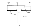
- FIG. 2 is a cross-sectional view taken along line AA ′ in FIG. It is a top view which shows the structure of the waveguide microstrip line converter based on Example 2 of this invention. It is a top view which shows the structure of the waveguide microstrip line converter based on Example 3 of this invention.
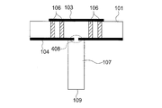
- FIG. 5 is a sectional view taken along line BB ′ in FIG. 4. It is a top view which shows the structure of the waveguide microstrip line converter based on Example 4 of this invention.
- FIG. 7 is a cross-sectional view taken along the line DD ′ in FIG.
- FIGS. 1 is a plan view showing a configuration of a waveguide microstrip line converter according to Embodiment 1 of the present invention.
- FIG. 2 is a cross-sectional view taken along line AA ′ in FIG. In the following, in each figure, the same reference numerals indicate the same or corresponding parts.
- a waveguide microstrip line converter includes a rectangular (rectangular) dielectric substrate 101, a strip conductor 102 formed on the surface of the dielectric substrate 101, and the like.
- the strip conductor 102 and the conductor plate 103 are connected by a connecting portion 105.
- a rectangular opening 108 is provided in the ground conductor 104 in the waveguide 107.
- the input / output end 109 of the waveguide 107 is shown on the lower side of FIG.
- the input / output end 110 of the microstrip line formed by the strip conductor 102 and the ground conductor 104 is shown on the left side of FIG.
- the post wall waveguide 111 includes a conductor plate 103, a ground conductor 104, and a connection conductor 106.
- the row interval D1 of the connection conductors 106 near the connection portion 105 is narrower than the row interval D2 of the connection conductors 106 near the opening 108 (D1 ⁇ D2).
- the high-frequency signal input from the input / output end 109 of the waveguide 107 is output to the post wall waveguide 111 through the opening 108.
- the high-frequency signal output to the post wall waveguide 111 is output from the input / output end 110 of the microstrip line via the connection unit 105.
- the arrangement of the connection conductors 106 is determined so as to be impedance matched.
- the first embodiment operates as a waveguide microstrip line converter.
- the column spacing D1 between the two rows of connection conductors 106 in the longitudinal direction of the microstrip line in the vicinity of the connection portion 105 is narrower than that in the vicinity of the opening 108. This has the effect of reducing the power radiated from the vicinity of 105 to the outside of the waveguide microstrip line converter.
- the size (shape) of the opening 108 is the same as that of the cross section of the waveguide 107.
- the present invention is not limited to this, and the opening 108 is disposed on the inner side of the cross section of the waveguide 107. It may be on the outside so as to cover the cross section of the waveguide 107. That is, the size (shape) of the opening 108 may be smaller or larger than the cross section of the waveguide 107.
- the conductor plate 103 is rectangular has been described.
- the present invention is not limited to this, and other shapes such as a circle and a polygon may be used.
- the present invention is not limited to this, and other shapes such as a circle and a polygon may be used.
- connection conductor 106 has a cylindrical shape
- connection conductor 106 has a cylindrical shape
- other shapes such as a quadrangular prism shape and a polygonal column shape may be used.
- the column spacing D 1 of the two rows of connection conductors 106 in the longitudinal direction of the microstrip line is smaller than that in the vicinity of the opening 108 of the waveguide 107.
- FIG. 3 is a plan view showing the configuration of the waveguide microstrip line converter according to Embodiment 2 of the present invention.
- the two notches 201 are provided in the conductor plate 103.
- Other configurations are the same as those of the first embodiment.
- the operation of the second embodiment is the same as that of the first embodiment. However, since impedance matching can be performed by adjusting the position and shape of the notch 201, there is an effect of facilitating impedance matching.
- FIGS. 4 is a plan view showing a configuration of a waveguide microstrip line converter according to Embodiment 3 of the present invention.
- FIG. 5 is a cross-sectional view taken along line BB ′ in FIG.
- This waveguide microstrip line converter has three input / output ends: an input / output end 109 of the waveguide 107 and input / output ends 306 and 307 of the microstrip line.
- the post wall waveguides 308 and 309 are constituted by the connection conductor 106, the ground conductor 104, and the conductor plate 103.
- a high-frequency signal input from the input / output end 109 of the waveguide 107 is output to the post wall waveguides 308 and 309 through the opening 108.
- the waveguide microstrip line converter according to the third embodiment has a symmetric structure in the section taken along the line CC ′ in FIG. 4, an electric wall can be assumed in the section taken along the line CC ′.
- High-frequency signals are output in opposite phases to the wall waveguides 308 and 309.
- the high-frequency signals output to the post wall waveguides 308 and 309 are output to the input / output ends 306 and 307 of the microstrip line via the connection portions 304 and 305, respectively.
- connection conductors 106 and the dimensions of the notches 201 are determined so as to be impedance matched.
- the third embodiment has an effect of realizing a waveguide microstrip line converter that outputs in opposite phase from two microstrip lines.
- the waveguide microstrip line converter according to the third embodiment passes through a plane parallel to the center of the signal propagation direction in the waveguide 107 and the tube wall, and through a plane perpendicular to the dielectric substrate 101.
- the cross section passes through a plane perpendicular to the longitudinal direction of the microstrip line (cross section taken along the line CC ′).
- a high-frequency signal is input from the input / output end 109 of the waveguide 107 and output to the input / output ends 306 and 307 of the microstrip line.
- high-frequency signals having opposite phases are input from 306 and 307 and output to the input / output end 109 of the waveguide 107.
- the opening 108 is rectangular has been described.
- the present invention is not limited to this, and other shapes such as a circle and a polygon may be used.
- FIG. 6 is a plan view showing a configuration of a waveguide microstrip line converter according to Embodiment 4 of the present invention.
- FIG. 7 is a cross-sectional view taken along the line DD ′ in FIG.
- the opening 408 is provided in the ground conductor 104 so as to be inside the cross section perpendicular to the propagation direction of the high-frequency signal in the waveguide 107.
- the operation of the fourth embodiment is the same as that of the third embodiment.
- the opening 408 is provided so as to be on the inner side of the cross section of the waveguide 107, the opening 408 is not affected even when the dielectric substrate 101 and the waveguide 107 are connected to be shifted from the design position at the time of manufacture. Since it exists in the cross section of the waveguide 107, there exists an effect that characteristic degradation is small.
Landscapes
- Waveguides (AREA)
- Waveguide Connection Structure (AREA)
Abstract
Description
Claims (4)
- 導波管と、
前記導波管の一端を覆うように接続された誘電体基板と、
前記誘電体基板の一方の面の端部に設けられたストリップ導体と、
前記誘電体基板の一方の面の略中央に設けられ、前記ストリップ導体に接続された導体板と、
前記導波管と前記誘電体基板の接続領域を除く、前記誘電体基板の他方の面に設けられた地導体と、
前記ストリップ導体と前記導体板を接続する部分を除く、前記導体板の周辺と前記地導体を接続する複数の接続導体とを備え、
前記導波管と前記誘電体基板の接続領域の前記地導体に開口を設け、
前記導体板は前記誘電体基板を介して前記開口を覆うように設け、
前記ストリップ導体と前記地導体でマイクロストリップ線路を形成し、
前記マイクロストリップ線路の長手方向に並び、かつ前記導体板の対抗する両側に設けられた2列の接続導体の列間隔を、前記開口付近よりも前記ストリップ導体と前記導体板の接続部付近の方が狭くなるように接続導体を配置する
ことを特徴とする導波管マイクロストリップ線路変換器。 - 前記ストリップ導体と前記導体板の接続部付近の前記導体板に切り欠きを設けた
ことを特徴とする請求項1記載の導波管マイクロストリップ線路変換器。 - 前記導波管内の信号伝搬方向の中心及び管壁に並行な面を通り、前記誘電体基板に対して垂直な面を通り、前記マイクロストリップ線路の長手方向に対して垂直な面を通る断面について対称構造である
ことを特徴とする請求項1又は2記載の導波管マイクロストリップ線路変換器。 - 前記開口は、前記導波管の信号伝搬方向に垂直な断面よりも内側に配置される
ことを特徴とする請求項1から請求項3までのいずれかに記載の導波管マイクロストリップ線路変換器。
Priority Applications (4)
| Application Number | Priority Date | Filing Date | Title |
|---|---|---|---|
| JP2011501544A JP5289551B2 (ja) | 2009-02-27 | 2010-02-05 | 導波管マイクロストリップ線路変換器 |
| US13/142,364 US8723616B2 (en) | 2009-02-27 | 2010-02-05 | Waveguide-microstrip line converter having connection conductors spaced apart by different distances |
| CN2010800071473A CN102318134A (zh) | 2009-02-27 | 2010-02-05 | 波导微带线转换器 |
| EP10746072.7A EP2403055B1 (en) | 2009-02-27 | 2010-02-05 | Waveguide-microstrip line converter |
Applications Claiming Priority (2)
| Application Number | Priority Date | Filing Date | Title |
|---|---|---|---|
| JP2009046365 | 2009-02-27 | ||
| JP2009-046365 | 2009-02-27 |
Publications (1)
| Publication Number | Publication Date |
|---|---|
| WO2010098191A1 true WO2010098191A1 (ja) | 2010-09-02 |
Family
ID=42665401
Family Applications (1)
| Application Number | Title | Priority Date | Filing Date |
|---|---|---|---|
| PCT/JP2010/051681 Ceased WO2010098191A1 (ja) | 2009-02-27 | 2010-02-05 | 導波管マイクロストリップ線路変換器 |
Country Status (5)
| Country | Link |
|---|---|
| US (1) | US8723616B2 (ja) |
| EP (1) | EP2403055B1 (ja) |
| JP (1) | JP5289551B2 (ja) |
| CN (2) | CN104485500B (ja) |
| WO (1) | WO2010098191A1 (ja) |
Cited By (4)
| Publication number | Priority date | Publication date | Assignee | Title |
|---|---|---|---|---|
| JP2012256967A (ja) * | 2011-06-07 | 2012-12-27 | Mitsubishi Electric Corp | 導波管マイクロストリップ線路変換器 |
| JP2014029987A (ja) * | 2012-07-04 | 2014-02-13 | Sumitomo Electric Device Innovations Inc | フレキシブル基板 |
| JP2017224887A (ja) * | 2016-06-13 | 2017-12-21 | 株式会社フジクラ | 給電装置 |
| WO2018008087A1 (ja) * | 2016-07-05 | 2018-01-11 | 三菱電機株式会社 | 導波管-平面導波路変換器 |
Families Citing this family (17)
| Publication number | Priority date | Publication date | Assignee | Title |
|---|---|---|---|---|
| EP2618421A1 (en) | 2012-01-19 | 2013-07-24 | Huawei Technologies Co., Ltd. | Surface Mount Microwave System |
| FR3010835B1 (fr) | 2013-09-19 | 2015-09-11 | Inst Mines Telecom Telecom Bretagne | Dispositif de jonction entre une ligne de transmission imprimee et un guide d'ondes dielectrique |
| US9515368B2 (en) * | 2014-03-11 | 2016-12-06 | Nxp B.V. | Transmission line interconnect |
| US10693236B2 (en) | 2016-02-03 | 2020-06-23 | Waymo Llc | Iris matched PCB to waveguide transition |
| EP3240101B1 (en) * | 2016-04-26 | 2020-07-29 | Huawei Technologies Co., Ltd. | Radiofrequency interconnection between a printed circuit board and a waveguide |
| JP6415790B2 (ja) * | 2016-07-05 | 2018-10-31 | 三菱電機株式会社 | 導波管−平面導波路変換器 |
| WO2019138468A1 (ja) | 2018-01-10 | 2019-07-18 | 三菱電機株式会社 | 導波管マイクロストリップ線路変換器およびアンテナ装置 |
| WO2019142314A1 (ja) * | 2018-01-19 | 2019-07-25 | 三菱電機株式会社 | 変換器およびアンテナ装置 |
| JP6851556B2 (ja) * | 2018-12-04 | 2021-03-31 | 三菱電機株式会社 | 導波管平面線路変換器及び高周波モジュール |
| CN109546276A (zh) * | 2018-12-17 | 2019-03-29 | 西安电子工程研究所 | 一种新型平面波导-微带转换结构 |
| JP6723412B1 (ja) * | 2019-05-10 | 2020-07-15 | 株式会社フジクラ | モード変換器 |
| FR3105454B1 (fr) * | 2019-12-18 | 2023-05-05 | Thales Sa | Dispositif de transmission d'un signal a un guide d'ondes |
| US12272857B2 (en) | 2020-03-06 | 2025-04-08 | Mitsubishi Electric Corporation | Waveguide microstrip line converter |
| DE102020119495A1 (de) * | 2020-07-23 | 2022-01-27 | Fraunhofer-Gesellschaft zur Förderung der angewandten Forschung eingetragener Verein | Hochfrequenz-Struktur mit substratintegriertem Wellenleiter und Rechteck-Hohlleiter |
| SE544398C2 (en) * | 2020-09-11 | 2022-05-10 | Saab Ab | A transition arrangement |
| DE112020007647T5 (de) * | 2020-10-01 | 2023-07-13 | Mitsubishi Electric Corporation | Wellenleiter-Mikrostreifenleitungswandler |
| JP2024064072A (ja) * | 2022-10-27 | 2024-05-14 | 古野電気株式会社 | 高周波回路、および、レーダ装置 |
Citations (5)
| Publication number | Priority date | Publication date | Assignee | Title |
|---|---|---|---|---|
| JP2003158408A (ja) * | 2001-11-20 | 2003-05-30 | Anritsu Corp | 給電器 |
| JP2003273612A (ja) * | 2002-03-13 | 2003-09-26 | Mitsubishi Electric Corp | 導波管/マイクロストリップ線路変換器 |
| JP3672241B2 (ja) | 2001-01-11 | 2005-07-20 | 三菱電機株式会社 | 導波管/マイクロストリップ線路変換器およびこれを用いた高周波パッケージ |
| JP2005318360A (ja) * | 2004-04-30 | 2005-11-10 | Tdk Corp | 導波管型導波路および高周波モジュール |
| JP2008271295A (ja) * | 2007-04-23 | 2008-11-06 | Kyocera Corp | マイクロストリップ線路と積層型導波管線路との接続構造体およびこれを有する配線基板 |
Family Cites Families (9)
| Publication number | Priority date | Publication date | Assignee | Title |
|---|---|---|---|---|
| US6242984B1 (en) | 1998-05-18 | 2001-06-05 | Trw Inc. | Monolithic 3D radial power combiner and splitter |
| US6396363B1 (en) * | 1998-12-18 | 2002-05-28 | Tyco Electronics Corporation | Planar transmission line to waveguide transition for a microwave signal |
| US20020097108A1 (en) * | 2000-12-07 | 2002-07-25 | Nitin Jain | Transmission line to waveguide mode transformer |
| US7064633B2 (en) * | 2002-07-13 | 2006-06-20 | The Chinese University Of Hong Kong | Waveguide to laminated waveguide transition and methodology |
| JP3891918B2 (ja) * | 2002-10-29 | 2007-03-14 | Tdk株式会社 | 高周波モジュール |
| JP2005260570A (ja) | 2004-03-11 | 2005-09-22 | Mitsubishi Electric Corp | マイクロストリップ線路導波管変換器 |
| ES2334566T3 (es) | 2004-04-29 | 2010-03-12 | Nokia Siemens Networks S.P.A. | Transicion de microcinta a guia de onda para ondas milimetricas incorporadas en una tarjeta de circuitos impresos multicapas. |
| US7479841B2 (en) * | 2005-02-15 | 2009-01-20 | Northrop Grumman Corporation | Transmission line to waveguide interconnect and method of forming same including a heat spreader |
| WO2010026990A1 (ja) | 2008-09-05 | 2010-03-11 | 三菱電機株式会社 | 高周波回路パッケージおよびセンサモジュール |
-
2010
- 2010-02-05 JP JP2011501544A patent/JP5289551B2/ja active Active
- 2010-02-05 CN CN201410797933.8A patent/CN104485500B/zh active Active
- 2010-02-05 CN CN2010800071473A patent/CN102318134A/zh active Pending
- 2010-02-05 EP EP10746072.7A patent/EP2403055B1/en active Active
- 2010-02-05 WO PCT/JP2010/051681 patent/WO2010098191A1/ja not_active Ceased
- 2010-02-05 US US13/142,364 patent/US8723616B2/en active Active
Patent Citations (5)
| Publication number | Priority date | Publication date | Assignee | Title |
|---|---|---|---|---|
| JP3672241B2 (ja) | 2001-01-11 | 2005-07-20 | 三菱電機株式会社 | 導波管/マイクロストリップ線路変換器およびこれを用いた高周波パッケージ |
| JP2003158408A (ja) * | 2001-11-20 | 2003-05-30 | Anritsu Corp | 給電器 |
| JP2003273612A (ja) * | 2002-03-13 | 2003-09-26 | Mitsubishi Electric Corp | 導波管/マイクロストリップ線路変換器 |
| JP2005318360A (ja) * | 2004-04-30 | 2005-11-10 | Tdk Corp | 導波管型導波路および高周波モジュール |
| JP2008271295A (ja) * | 2007-04-23 | 2008-11-06 | Kyocera Corp | マイクロストリップ線路と積層型導波管線路との接続構造体およびこれを有する配線基板 |
Cited By (6)
| Publication number | Priority date | Publication date | Assignee | Title |
|---|---|---|---|---|
| JP2012256967A (ja) * | 2011-06-07 | 2012-12-27 | Mitsubishi Electric Corp | 導波管マイクロストリップ線路変換器 |
| JP2014029987A (ja) * | 2012-07-04 | 2014-02-13 | Sumitomo Electric Device Innovations Inc | フレキシブル基板 |
| JP2017224887A (ja) * | 2016-06-13 | 2017-12-21 | 株式会社フジクラ | 給電装置 |
| WO2018008087A1 (ja) * | 2016-07-05 | 2018-01-11 | 三菱電機株式会社 | 導波管-平面導波路変換器 |
| JPWO2018008087A1 (ja) * | 2016-07-05 | 2018-10-18 | 三菱電機株式会社 | 導波管−平面導波路変換器 |
| US11069949B2 (en) | 2016-07-05 | 2021-07-20 | Mitsubishi Electric Corporation | Hollow-waveguide-to-planar-waveguide transition circuit comprising a coupling conductor disposed over slots in a ground conductor |
Also Published As
| Publication number | Publication date |
|---|---|
| CN104485500B (zh) | 2018-11-06 |
| JPWO2010098191A1 (ja) | 2012-08-30 |
| US8723616B2 (en) | 2014-05-13 |
| EP2403055A1 (en) | 2012-01-04 |
| CN102318134A (zh) | 2012-01-11 |
| US20110267153A1 (en) | 2011-11-03 |
| EP2403055A4 (en) | 2013-07-03 |
| EP2403055B1 (en) | 2019-11-06 |
| CN104485500A (zh) | 2015-04-01 |
| JP5289551B2 (ja) | 2013-09-11 |
Similar Documents
| Publication | Publication Date | Title |
|---|---|---|
| JP5289551B2 (ja) | 導波管マイクロストリップ線路変換器 | |
| JP6591091B2 (ja) | 導波管マイクロストリップ線路変換器 | |
| CN104221217B (zh) | 波导管缝隙阵列天线装置 | |
| JP5007281B2 (ja) | 誘電体導波管スロットアンテナ | |
| US9385428B2 (en) | Metamaterial structure | |
| JP6470930B2 (ja) | 分配器及び平面アンテナ | |
| JP4833026B2 (ja) | 導波管の接続構造 | |
| JP5566169B2 (ja) | アンテナ装置 | |
| US11316273B2 (en) | Antenna device | |
| US10811753B2 (en) | Hollow-waveguide-to-planar-waveguide transition including a coupling conductor having one or more conductors branching therefrom | |
| US11387534B2 (en) | Converter and antenna device | |
| JP5705035B2 (ja) | 導波管マイクロストリップ線路変換器 | |
| JP2011015044A (ja) | 導波管のチョークフランジ、及びその製造方法 | |
| JP2026507362A (ja) | 多層導波管移行部 | |
| EP3276741B1 (en) | Waveguide tube/transmission line converter and antenna device | |
| JP5377070B2 (ja) | 導波管/マイクロストリップ線路変換器 | |
| JP4542066B2 (ja) | 導波管電力分配器 | |
| JP4869306B2 (ja) | 伝送線路構造物 |
Legal Events
| Date | Code | Title | Description |
|---|---|---|---|
| WWE | Wipo information: entry into national phase |
Ref document number: 201080007147.3 Country of ref document: CN |
|
| 121 | Ep: the epo has been informed by wipo that ep was designated in this application |
Ref document number: 10746072 Country of ref document: EP Kind code of ref document: A1 |
|
| WWE | Wipo information: entry into national phase |
Ref document number: 2011501544 Country of ref document: JP |
|
| WWE | Wipo information: entry into national phase |
Ref document number: 13142364 Country of ref document: US |
|
| WWE | Wipo information: entry into national phase |
Ref document number: 2010746072 Country of ref document: EP |
|
| NENP | Non-entry into the national phase |
Ref country code: DE |