WO2010110196A1 - ダイヤモンド薄膜を被覆した炭素材料及びその製造方法 - Google Patents
ダイヤモンド薄膜を被覆した炭素材料及びその製造方法 Download PDFInfo
- Publication number
- WO2010110196A1 WO2010110196A1 PCT/JP2010/054768 JP2010054768W WO2010110196A1 WO 2010110196 A1 WO2010110196 A1 WO 2010110196A1 JP 2010054768 W JP2010054768 W JP 2010054768W WO 2010110196 A1 WO2010110196 A1 WO 2010110196A1
- Authority
- WO
- WIPO (PCT)
- Prior art keywords
- diamond
- carbon material
- diamond grains
- carbonaceous substrate
- substrate
- Prior art date
- Legal status (The legal status is an assumption and is not a legal conclusion. Google has not performed a legal analysis and makes no representation as to the accuracy of the status listed.)
- Ceased
Links
Images


Classifications
-
- C—CHEMISTRY; METALLURGY
- C01—INORGANIC CHEMISTRY
- C01B—NON-METALLIC ELEMENTS; COMPOUNDS THEREOF; METALLOIDS OR COMPOUNDS THEREOF NOT COVERED BY SUBCLASS C01C
- C01B32/00—Carbon; Compounds thereof
- C01B32/25—Diamond
-
- C—CHEMISTRY; METALLURGY
- C01—INORGANIC CHEMISTRY
- C01B—NON-METALLIC ELEMENTS; COMPOUNDS THEREOF; METALLOIDS OR COMPOUNDS THEREOF NOT COVERED BY SUBCLASS C01C
- C01B32/00—Carbon; Compounds thereof
- C01B32/25—Diamond
- C01B32/26—Preparation
-
- C—CHEMISTRY; METALLURGY
- C23—COATING METALLIC MATERIAL; COATING MATERIAL WITH METALLIC MATERIAL; CHEMICAL SURFACE TREATMENT; DIFFUSION TREATMENT OF METALLIC MATERIAL; COATING BY VACUUM EVAPORATION, BY SPUTTERING, BY ION IMPLANTATION OR BY CHEMICAL VAPOUR DEPOSITION, IN GENERAL; INHIBITING CORROSION OF METALLIC MATERIAL OR INCRUSTATION IN GENERAL
- C23C—COATING METALLIC MATERIAL; COATING MATERIAL WITH METALLIC MATERIAL; SURFACE TREATMENT OF METALLIC MATERIAL BY DIFFUSION INTO THE SURFACE, BY CHEMICAL CONVERSION OR SUBSTITUTION; COATING BY VACUUM EVAPORATION, BY SPUTTERING, BY ION IMPLANTATION OR BY CHEMICAL VAPOUR DEPOSITION, IN GENERAL
- C23C16/00—Chemical coating by decomposition of gaseous compounds, without leaving reaction products of surface material in the coating, i.e. chemical vapour deposition [CVD] processes
- C23C16/02—Pretreatment of the material to be coated
- C23C16/0272—Deposition of sub-layers, e.g. to promote the adhesion of the main coating
-
- C—CHEMISTRY; METALLURGY
- C23—COATING METALLIC MATERIAL; COATING MATERIAL WITH METALLIC MATERIAL; CHEMICAL SURFACE TREATMENT; DIFFUSION TREATMENT OF METALLIC MATERIAL; COATING BY VACUUM EVAPORATION, BY SPUTTERING, BY ION IMPLANTATION OR BY CHEMICAL VAPOUR DEPOSITION, IN GENERAL; INHIBITING CORROSION OF METALLIC MATERIAL OR INCRUSTATION IN GENERAL
- C23C—COATING METALLIC MATERIAL; COATING MATERIAL WITH METALLIC MATERIAL; SURFACE TREATMENT OF METALLIC MATERIAL BY DIFFUSION INTO THE SURFACE, BY CHEMICAL CONVERSION OR SUBSTITUTION; COATING BY VACUUM EVAPORATION, BY SPUTTERING, BY ION IMPLANTATION OR BY CHEMICAL VAPOUR DEPOSITION, IN GENERAL
- C23C16/00—Chemical coating by decomposition of gaseous compounds, without leaving reaction products of surface material in the coating, i.e. chemical vapour deposition [CVD] processes
- C23C16/22—Chemical coating by decomposition of gaseous compounds, without leaving reaction products of surface material in the coating, i.e. chemical vapour deposition [CVD] processes characterised by the deposition of inorganic material, other than metallic material
- C23C16/26—Deposition of carbon only
- C23C16/27—Diamond only
- C23C16/271—Diamond only using hot filaments
-
- C—CHEMISTRY; METALLURGY
- C23—COATING METALLIC MATERIAL; COATING MATERIAL WITH METALLIC MATERIAL; CHEMICAL SURFACE TREATMENT; DIFFUSION TREATMENT OF METALLIC MATERIAL; COATING BY VACUUM EVAPORATION, BY SPUTTERING, BY ION IMPLANTATION OR BY CHEMICAL VAPOUR DEPOSITION, IN GENERAL; INHIBITING CORROSION OF METALLIC MATERIAL OR INCRUSTATION IN GENERAL
- C23C—COATING METALLIC MATERIAL; COATING MATERIAL WITH METALLIC MATERIAL; SURFACE TREATMENT OF METALLIC MATERIAL BY DIFFUSION INTO THE SURFACE, BY CHEMICAL CONVERSION OR SUBSTITUTION; COATING BY VACUUM EVAPORATION, BY SPUTTERING, BY ION IMPLANTATION OR BY CHEMICAL VAPOUR DEPOSITION, IN GENERAL
- C23C16/00—Chemical coating by decomposition of gaseous compounds, without leaving reaction products of surface material in the coating, i.e. chemical vapour deposition [CVD] processes
- C23C16/22—Chemical coating by decomposition of gaseous compounds, without leaving reaction products of surface material in the coating, i.e. chemical vapour deposition [CVD] processes characterised by the deposition of inorganic material, other than metallic material
- C23C16/26—Deposition of carbon only
- C23C16/27—Diamond only
- C23C16/277—Diamond only using other elements in the gas phase besides carbon and hydrogen; using other elements besides carbon, hydrogen and oxygen in case of use of combustion torches; using other elements besides carbon, hydrogen and inert gas in case of use of plasma jets
-
- Y—GENERAL TAGGING OF NEW TECHNOLOGICAL DEVELOPMENTS; GENERAL TAGGING OF CROSS-SECTIONAL TECHNOLOGIES SPANNING OVER SEVERAL SECTIONS OF THE IPC; TECHNICAL SUBJECTS COVERED BY FORMER USPC CROSS-REFERENCE ART COLLECTIONS [XRACs] AND DIGESTS
- Y10—TECHNICAL SUBJECTS COVERED BY FORMER USPC
- Y10T—TECHNICAL SUBJECTS COVERED BY FORMER US CLASSIFICATION
- Y10T428/00—Stock material or miscellaneous articles
- Y10T428/27—Web or sheet containing structurally defined element or component, the element or component having a specified weight per unit area [e.g., gms/sq cm, lbs/sq ft, etc.]
- Y10T428/273—Web or sheet containing structurally defined element or component, the element or component having a specified weight per unit area [e.g., gms/sq cm, lbs/sq ft, etc.] of coating
Definitions
- the present invention relates to a carbon material obtained by synthesizing a diamond thin film on a carbonaceous substrate and a manufacturing method thereof.
- Diamond has significant characteristics in strength, thermal conductivity, chemical resistance, etc., and has a very high potential for application development mainly for industrial materials that exhibit their physical properties.
- CVD diamond has been around for a long time since the discovery of its film-forming method, and has already been used mainly for cutting and grinding as industrial applications, including heat dissipation substrates (for electronic circuit components), sensors (working in harsh environments), optical window materials, Active in a wide range of fields such as detectors (for particle physics experiments), speaker diaphragms, etc. The use is expected to expand further in the future.
- Diamond production methods for industrial applications can be broadly classified into high-pressure synthesis methods and gas phase synthesis methods.
- the former is a method of simulating the formation of diamond in nature by converting graphite to diamond by applying high temperature and high pressure to graphite as a carbon source that is a raw material of diamond, for example.
- the latter is a constituent element of diamond. This is a technique in which a raw material derived from a certain carbon is converted into a diamond state on a substrate through a chemical reaction including excitation and decomposition via electromagnetic waves or a heating element, in a gas state.
- a plasma CVD plasma-asymmetric chemical vapor deposition
- a hot filament CVD HFCVD
- a flame flame Chamb
- the difference between these methods is that they are due to electrons, ions, radical species, or heating elements, or thermal energy in the plasma as a means of molecular decomposition / excitation in the gas phase space. Is in a different point.
- the diamond synthesized by the above method has a film-like form, and the diamond can be obtained by transferring the surface shape of the coating material. Further, by selecting a gas species as a raw material, it is possible to contain (doping) impurities such as boron, phosphorus and nitrogen in the film, and the film into which these elements are introduced is electrically semiconductive. Shows behavior and eventually changes its properties to conductors with increasing content.
- CVD diamond when CVD diamond is formed on various carbonaceous substrates, there is a difference in thermal expansion coefficient between the substrate and the CVD diamond layer, and if there is an excessive difference in thermal expansion coefficient, the film is formed.
- the CVD diamond layer In the temperature lowering step after preparation, the CVD diamond layer is subjected to stress in the compressing or pulling direction with respect to the base material, and thus may be peeled off.
- the substrate surface is roughened to mechanically anchor and hold the diamond layer.
- the technique to do has been examined.
- a method of forming a diamond layer on a base material by a CVD method there is a method of forming a film by the CVD method on unevenness generated by roughening the surface of the base material by blasting described in Patent Document 1 below.
- a film is formed in a form in which the uneven surface is transferred, and at the same time the contact area is increased, the substrate is fixed (anchored) by hitting the wedge against the film, and the adhesion between the film and the substrate is increased Increase.
- the treatment by this method can prevent peeling due to expansion and contraction of the film due to the difference in thermal expansion coefficient between the film and the base material, and can prevent the occurrence of cracks, and is practiced as a very useful surface treatment technique. .
- the present invention provides a carbon material including a diamond thin film having excellent adhesion and suppressing a substrate etching rate by attaching diamond grains that are hardly affected by etching by hydrogen radicals on a carbonaceous substrate.
- the object is to provide a manufacturing method.
- the present invention provides a carbon material in which diamond grains are arranged on the surface of a carbonaceous substrate, and further a diamond layer having the diamond grains as a nucleus is formed.
- the weight per area is regulated to 1.0 ⁇ 10 ⁇ 4 g / cm 2 or more and less than 3.0 ⁇ 10 ⁇ 3 g / cm 2 .
- the weight is less than 1.0 ⁇ 10 ⁇ 4 g / cm 2 , the amount of the diamond grains is too small, and the carbonaceous substrate While the effect of arranging the diamond grains on the surface of the material is not sufficiently exhibited, when the weight is 3.0 ⁇ 10 ⁇ 3 g / cm 2 or more, the adhesion between the diamond thin film and the carbonaceous substrate cannot be obtained. This is because inconvenience of peeling occurs.
- the weight per unit area of the diamond grains is restricted to 2.3 ⁇ 10 ⁇ 4 g / cm 2 or more.
- the carbonaceous substrate When the carbonaceous substrate is solid in a diamond synthesis atmosphere, it is desirable that a weight loss of ⁇ 4.0% or less is observed. Further, the carbonaceous substrate is made of a one-component or binary material.
- the diamond layer contains at least one conductivity imparting element selected from the group consisting of nitrogen, boron and phosphorus, and the electrical resistance of the layer is regulated to 1 ⁇ 10 ⁇ 3 ⁇ ⁇ cm or more. Is desirable. In order to produce a diamond layer having an electric resistance of less than 1 ⁇ 10 ⁇ 3 ⁇ ⁇ cm, the ratio of the source gas concentration B (boron) / C (carbon) needs to exceed 10,000 ppm. It is difficult, and since excessive dopants may significantly inhibit the formation of the diamond layer by crystal growth, it is desirable to regulate as described above. This applies not only to boron but also to nitrogen and phosphorus.
- the step of producing diamond grains and the weight per unit area are 1.0 ⁇ 10 ⁇ 4 g / cm 2 or more and less than 3.0 ⁇ 10 ⁇ 3 g / cm 2.
- the method has a step of arranging diamond grains on the surface of the carbonaceous substrate and a step of forming a diamond layer having the diamond grains as nuclei by a vapor phase synthesis method.
- the carbon material can be produced by such a method.
- a diamond as a nucleus is not necessary, but synthesis of a diamond having a large shape is difficult, and several mm is the maximum.
- the diamond particles are arranged by ultrasonic attachment (ultrasonic method) or spray method using a solution in which the diamond particles are dispersed. More preferably, it is done by law.
- the solution for dispersing the diamond particles can be dispersed using alcohols such as ethanol, butanol, isopropanol, acetonitrile, water, pure, polyvinyl alcohol solution, etc., but the solvent can be removed at low temperature and the diamond particles can be removed. It is preferable to use ethanol in which is relatively dispersed. According to this method, a layer of diamond grains can be easily formed on the surface of the carbonaceous substrate, and the adhesion between the carbonaceous substrate, diamond grains and the diamond thin film can be maintained well. is there.
- the carbonaceous material having a diamond thin film with excellent adhesion and suppressing the substrate etching rate.
- the excellent effect that a base material and its manufacturing method can be provided is produced.
- diamond particles (average secondary particle diameter: 1 ⁇ m) are prepared by a high-pressure synthesis method, and then an ethanol solution in which the diamond particles are dispersed at a ratio of 1.0 wt% is prepared. Diamond particles were attached to the substrate. At that time, the weight per unit area of the diamond grains (diamond seed crystals) on the substrate surface was 2.3 ⁇ 10 ⁇ 4 g / cm 2 .
- a diamond layer having the above diamond grains as nuclei was formed under the following conditions.
- Filament type Tungsten Filament temperature: 2400 ° C
- the obtained diamond thin film (diamond layer) was subjected to Raman spectroscopic analysis, a peak due to diamond was observed at 1333 cm ⁇ 1 . Further, when the obtained diamond thin film was observed with an SEM, the surface of the base material was covered with the diamond thin film, and it was a polycrystalline film composed of diamond grains having a self-shape with a grain size of about 1 ⁇ m. It was confirmed.
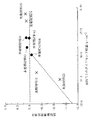
- FIG. 1 shows the rate of change in weight when the carbonaceous substrates I to V are exposed to the conditions of the hot filament CVD method without adding diamond grains.
- a carbonaceous substrate having a smaller crystallite size obtained from a diffraction line having a lower angle than the vicinity of 26 ° shows a change in weight reduction. This indicates that the highly reactive crystallite end face (edge face) reacts with hydrogen radicals. This indicates that the carbonaceous substrate is easy to be etched and easily etched by hydrogen gas.
- Example 1 A carbon material manufactured by the method shown in the embodiment for carrying out the invention was used.
- the carbon material thus produced is hereinafter referred to as the present invention material A1.
- the carbonaceous substrate I that is most easily etched is used as the carbonaceous substrate.
- Example 2 A carbon material was produced in the same manner as in Example 1 except that the ratio of diamond particles in the ethanol solution was 1.0 wt% and diamond particles were attached to the carbonaceous substrate I by a spray method.
- the carbon material thus produced is hereinafter referred to as the present invention material A2.
- the diamond particle concentration on the substrate surface was 5.7 ⁇ 10 ⁇ 4 g / cm 2 .
- the obtained diamond thin film was subjected to Raman spectroscopic analysis, a peak due to diamond was observed at 1333 cm ⁇ 1 . Furthermore, when the obtained diamond thin film was observed with an SEM, the surface of the base material was covered with the diamond thin film, and it was a polycrystalline film made of diamond grains having a self-shape with a grain size of about 1 ⁇ m. It was confirmed.
- Example 3 A carbon material was produced in the same manner as in Example 1 except that the ratio of the diamond grains in the ethanol solution was 2.0 wt%.
- the carbon material thus produced is hereinafter referred to as the present invention material A3.
- the diamond particle concentration on the substrate surface was 6.0 ⁇ 10 ⁇ 4 g / cm 2 .
- Example 4 A carbon material was produced in the same manner as in Example 1 except that the proportion of diamond grains in the ethanol solution was 0.05 wt%.
- the carbon material thus produced is hereinafter referred to as the present invention material A4.
- the diamond particle concentration on the substrate surface was 1.1 ⁇ 10 ⁇ 4 g / cm 2 .
- Example 5 A carbon material was prepared in the same manner as in Example 1 except that the proportion of diamond particles in the ethanol solution was 5.0 wt% and diamond particles were attached to the carbonaceous substrate V by a spray method.
- the carbon material thus produced is hereinafter referred to as the present invention material B1.
- the diamond particle concentration on the substrate surface was 2.3 ⁇ 10 ⁇ 4 g / cm 2 .
- Comparative Example 1 A carbon material was produced in the same manner as in Example 1 except that diamond particles were not added.
- the carbon material thus produced is hereinafter referred to as a comparative material Z1.
- Comparative Example 2 A carbon material was produced in the same manner as in Example 1 except that the proportion of diamond grains in the ethanol solution was 0.01 wt%.
- the carbon material thus produced is hereinafter referred to as comparative material Z2.
- the diamond particle concentration on the substrate surface was 1.0 ⁇ 10 ⁇ 5 g / cm 2 .
- Example 3 A carbon material was produced in the same manner as in Example 1 except that the proportion of diamond particles in the ethanol solution was 0.01 wt%.
- the carbon material thus produced is hereinafter referred to as a comparative material Z3.
- the diamond particle concentration on the substrate surface was 2.0 ⁇ 10 ⁇ 5 g / cm 2 .
- Example 4 A carbon material was produced in the same manner as in Example 1 except that the proportion of diamond particles in the ethanol solution was 5.0 wt%.
- the carbon material thus produced is hereinafter referred to as a comparative material Z4.
- the diamond particle concentration on the substrate surface was 3.0 ⁇ 10 ⁇ 3 g / cm 2 .
- Comparative Example 5 A carbon material was produced in the same manner as in Example 1 except that the proportion of diamond particles in the ethanol solution was 10.0 wt%.
- the carbon material thus produced is hereinafter referred to as comparative material Z5.
- the diamond particle concentration on the substrate surface was 6.0 ⁇ 10 ⁇ 3 g / cm 2 .
- the diamond layer peels off at the interface with the base material, and the weight of the base material is reduced after the formation of the diamond layer before the formation of the diamond layer.
- the weight of the base material is increased after the formation of the diamond layer than before the formation of the diamond layer, but the diamond layer peels off at the interface with the base material.
- the weight of the substrate is increased after the formation of the diamond layer than before the formation of the diamond layer, and the material is peeled off at the interface between the diamond layer and the substrate. It is recognized that there is not.
- material A4 although the substrate weight is slightly reduced after the formation than before the formation of the diamond layer, it is recognized that no peeling occurs at the interface between the diamond layer and the substrate.
- the substrate weight is increased after the formation of the diamond layer than before the diamond layer, It can be seen that no peeling occurs at the interface between the diamond layer and the substrate.
- the B / C ratio is desirably 10,000 ppm or less (resistance is 0.001 ⁇ cm or more).
- the present invention is obtained by imparting the characteristics of diamond or conductive diamond to a carbon material, and can be used for a fluorine generating electrolytic electrode, a work for electric discharge machining, and a heat sink material utilizing heat conduction and insulation. .
Landscapes
- Chemical & Material Sciences (AREA)
- Organic Chemistry (AREA)
- Engineering & Computer Science (AREA)
- Inorganic Chemistry (AREA)
- Chemical Kinetics & Catalysis (AREA)
- General Chemical & Material Sciences (AREA)
- Materials Engineering (AREA)
- Mechanical Engineering (AREA)
- Metallurgy (AREA)
- Life Sciences & Earth Sciences (AREA)
- General Life Sciences & Earth Sciences (AREA)
- Geology (AREA)
- Combustion & Propulsion (AREA)
- Plasma & Fusion (AREA)
- Physics & Mathematics (AREA)
- Crystals, And After-Treatments Of Crystals (AREA)
- Carbon And Carbon Compounds (AREA)
- Chemical Vapour Deposition (AREA)
Abstract
Description
尚、ダイヤモンド粒の単位面積当たりの重量を上記範囲に規制するのは、当該重量が1.0×10⁻⁴g/cm2未満であると、ダイヤモンド粒の量が少な過ぎて、炭素質基材の表面にダイヤモンド粒を配置した効果が十分に発揮されない一方、当該重量が3.0×10-3g/cm2以上になると、ダイヤモンド薄膜と炭素質基材との密着性が得られなくなり剥離するという不都合を生じるからである。
このように規制すれば、ダイヤモンド層の形成後に炭素質基材の重量が減少するのを抑制しつつ、ダイヤモンド層が炭素質基材から剥離するのを防止できる。
格子定数を0.36nm以下に規制するのは、この値を超えた場合にはダイヤモンドとしての結晶性が悪く水素ラジカルによるエッチングの影響を受けやすいからである。また、クラスター分布を0.003μm以上に規制するのは、0.003μm未満のダイヤモンド粒は気相合成雰囲気下においてガスの流れによりチャンバー中に対流してしまう可能性がある一方、クラスター分布を10μm以下に規制するのは、10μmを超えると炭素質基材に対する付着力が小さくなるからである。
電気抵抗が1×10⁻³Ω・cm未満とするダイヤモンド層を作製するには、原料ガス濃度B(ホウ素)/C(炭素)の比率が10000ppmを超える必要があるが、現在の装置性能から困難であり、また、過剰なドーパントは結晶成長によるダイヤモンド層の形成を著しく阻害する恐れがあるので、上記の如く規制するのが望ましい。尚、このことはホウ素に限らず、窒素、リンでも同様である。
このような方法により、上記炭素材料を作製することができる。
ここで、高圧合成法によるダイヤモンドの合成においては、核となるダイヤモンドは必要ではないが、大きな形状のダイヤモンドの合成は難しく、数mmが最大である。一方、気相合成法によるダイヤモンドの合成においては、大きな形状の基材上にダイヤモンドの合成を行うことは可能であるが、成膜速度と製造コストの観点から、核となるダイヤモンドが必要となる。こうして得られたダイヤモンド薄膜を粉砕することでダイヤモンド粒を作製することも可能である。したがって、上記構成の如く、ダイヤモンド粒を作製し、これを炭素質基材の表面に配置した後、気相合成法によりダイヤモンド層を形成することにより、炭素質基材とダイヤモンド層との密着性を維持しつつ、広範囲にダイヤモンドを円滑に作製できる。尚、ダイヤモンド粒における単位面積当たりの重量を、1.0×10⁻⁴g/cm2以上3.0×10-3g/cm2未満に規制するのは、上述した理由によるものである。
ダイヤモンド粒を分散させる溶液としては、エタノール、ブタノール、イソプロパノールなどのアルコール類、アセトニトリル、水、純粋、ポリビニルアルコール溶液などを用いて分散させることができるが、低温で溶媒が除去可能であってダイヤモンド粒が比較的分散するエタノールを用いるのが好ましい。
当該方法によれば、炭素質基材の表面にダイヤモンド粒の層を簡単に形成することができ、しかも、炭素質基材とダイヤモンド粒とダイヤモンド薄膜との接着性が良好に保たれるからである。
フィラメント温度:2400℃
原料ガス:水素ガス、メタンガス、トリメチルボロンガス(尚、B〔ホウ素〕/C〔炭素〕=1000ppmの比率となるように、メタンガス、トリメチルボロンガスとで導入)
炉内圧力:50Torr
処理時間:11時間
〔下記実施例及び比較例で用いる炭素質基材について〕
下記表1は、下記実施例及び比較例で用いる炭素質基材の結晶子サイズを示したものである。炭素質基材I~Vは、一元系若しくは二元系の炭素質原料からなり、X線回折図形において2θ=10~30°に現れる(002)回折線の形状が非対称であり、少なくとも2θ=26°付近と前記26°付近よりも低角の回折線の2本の成分図形を有する炭素質基材である。

上記発明を実施するための形態で示した方法により作製した炭素材料を用いた。
このようにして作製した炭素材料を、以下、本発明材料A1と称する。
尚、炭素質基材には、最もエッチングされ易い炭素質基材Iを用いている。
エタノール溶液中のダイヤモンド粒の割合を1.0wt%とし、且つ、スプレー法により炭素質基材Iにダイヤモンド粒を添着させた他は、上記実施例1と同様にして炭素材料を作製した。
このようにして作製した炭素材料を、以下、本発明材料A2と称する。
尚、炭素質基材にダイヤモンド粒を添着したとき、基材表面におけるダイヤモンド粒濃度は、5.7×10⁻⁴g/cm2であった。
エタノール溶液中のダイヤモンド粒の割合を2.0wt%とした他は、上記実施例1と同様にして炭素材料を作製した。
このようにして作製した炭素材料を、以下、本発明材料A3と称する。
尚、炭素質基材にダイヤモンド粒を添着したとき、基材表面におけるダイヤモンド粒濃度は、6.0×10⁻⁴g/cm2であった。
エタノール溶液のダイヤモンド粒の割合を0.05wt%とした他は、上記実施例1と同様にして炭素材料を作製した。
このようにして作製した炭素材料を、以下、本発明材料A4と称する。
尚、炭素質基材にダイヤモンド粒を添着したとき、基材表面におけるダイヤモンド粒濃度は、1.1×10⁻⁴g/cm2であった。
エタノール溶液中のダイヤモンド粒の割合を5.0wt%とし、且つ、スプレー法により炭素質基材Vにダイヤモンド粒を添着させた他は、上記実施例1と同様にして炭素材料を作製した。
このようにして作製した炭素材料を、以下、本発明材料B1と称する。
尚、炭素質基材にダイヤモンド粒を添着したとき、基材表面におけるダイヤモンド粒濃度は、2.3×10⁻⁴g/cm2であった。
ダイヤモンド粒を添着しない他は、上記実施例1と同様にして炭素材料を作製した。
このようにして作製した炭素材料を、以下、比較材料Z1と称する。
エタノール溶液中のダイヤモンド粒の割合を0.01wt%とした他は、上記実施例1と同様にして炭素材料を作製した。
このようにして作製した炭素材料を、以下、比較材料Z2と称する。
尚、炭素質基材にダイヤモンド粒を添着したとき、基材表面におけるダイヤモンド粒濃度は、1.0×10⁻⁵g/cm2であった。
エタノール溶液のダイヤモンド粒の割合を0.01wt%とした他は、上記実施例1と同様にして炭素材料を作製した。
このようにして作製した炭素材料を、以下、比較材料Z3と称する。
尚、炭素質基材にダイヤモンド粒を添着したとき、基材表面におけるダイヤモンド粒濃度は、2.0×10⁻⁵g/cm2であった。
エタノール溶液のダイヤモンド粒の割合を5.0wt%とした他は、上記実施例1と同様にして炭素材料を作製した。
このようにして作製した炭素材料を、以下、比較材料Z4と称する。
尚、炭素質基材にダイヤモンド粒を添着したとき、基材表面におけるダイヤモンド粒濃度は、3.0×10⁻³g/cm2であった。
エタノール溶液のダイヤモンド粒の割合を10.0wt%とした他は、上記実施例1と同様にして炭素材料を作製した。
このようにして作製した炭素材料を、以下、比較材料Z5と称する。
尚、炭素質基材にダイヤモンド粒を添着したとき、基材表面におけるダイヤモンド粒濃度は、6.0×10⁻³g/cm2であった。
上記本発明材料A1~A4、B1及び比較材料Z1~Z5について、ダイヤモンド薄膜の可否及び基材重量変化率について調べたので、それらの結果を、表2及び図2に示す。
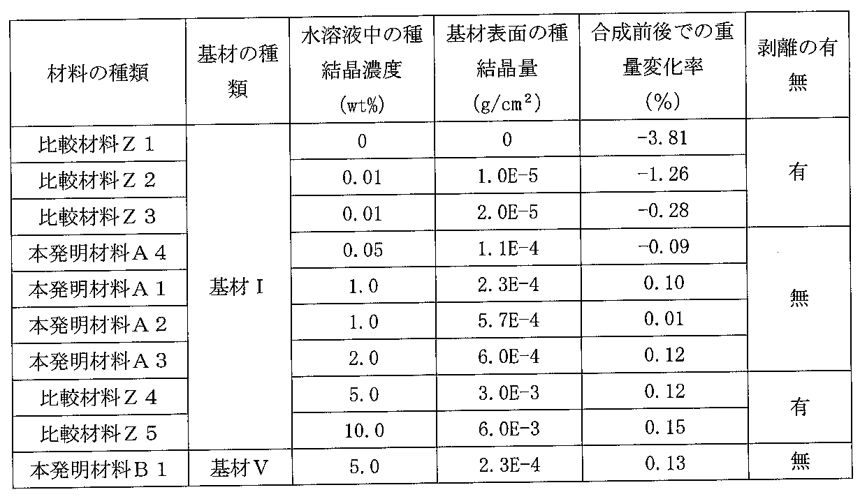
これに対して、本発明材料A1、A2、A3では、ダイヤモンド層の形成前よりも形成後の方が基材重量が増加しており、しかも、ダイヤモンド層と基材との界面で剥離していないことが認められる。また、本発明材料A4では、ダイヤモンド層の形成前よりも形成後の方が基材重量が若干減少しているものの、ダイヤモンド層と基材との界面で剥離していないことが認められる。
上記本発明材料A1を作製する際に、B〔ホウ素〕/C〔炭素〕の比率(以下、B/C比率と称する)を変えてメタンガスとトリメチルボロンガスとを導入し、作製された炭素材料の抵抗を調べたので、その結果を図2に示す。
図3から明らかなように、B/C比率が10000ppmでホウ素量が飽和に近づきつつあるので、それ以上にホウ素を添加しても、極めて大量に添加しない限り抵抗の大幅な減少は望めないことがわかる。加えて、B/C比率が10000ppmであっても、ダイヤモンドの結晶性は若干阻害されるため、これ以上B/C比率が大きくなると、結晶成長によるダイヤモンド層の形成が著しく阻害される恐れがある。したがって、B/C比率が10000ppm以下(抵抗は0.001Ωcm以上)であることが望ましい。
上記本発明材料A1、A2をフッ素発生用電解電極として用い、その電極性能について調べたので、その結果を以下に示す。
尚、実験は、本発明材料A1、A2を建浴直後のKF-2HF系溶融塩中に陽極として取り付ける一方、ニッケル板を陰極として取り付け、電流密度20A/dm2で定電流電解を実施した。
その結果、電解24時間後の槽電圧は5.6Vであった。そして、引き続き電解を継続し、更に24時間経過した後の槽電圧は5.6Vであり、時間経過により槽電圧は変化しないことが認められた。さらに、48時間経過後の陽極発生ガスを分析したところ、発生ガスはF2で発生効率は98%であることが認められた。
Claims (9)
- 炭素質基材の表面にダイヤモンド粒が配置され、更に、このダイヤモンド粒を核とするダイヤモンド層が形成された炭素材料であって、
上記ダイヤモンド粒の単位面積当たりの重量が、1.0×10⁻⁴g/cm2以上3.0×10-3g/cm2未満に規制されることを特徴とする炭素材料。 - 上記ダイヤモンド粒の単位面積当たりの重量が、2.3×10⁻⁴g/cm2以上に規制される、請求項1に記載の炭素材料。
- 前記ダイヤモンド粒は結晶性を有すると共に、XRDから得られる格子定数が0.36nm以下であって、しかも0.003μm以上10μm以下のクラスター分布を有する、請求項1又は2に記載の炭素材料。
- 上記炭素質基材は、ダイヤモンド合成雰囲気において無垢の場合には-4.0%以下の重量減少がみられる、請求項1~3の何れか1項に記載の炭素材料。
- 上記炭素質基材は、一元系若しくは二元系の原料からなる炭素質であり、X線回折図形において2θ=10~30°に現れる(002)回折線の形状が非対称であり、且つ、少なくとも2θ=26°付近とこの26°付近よりも低角の回折線の2本の成分図形を有する、請求項1~4の何れか1項に記載の炭素材料。
- 上記炭素質基材は、上記26°付近よりも低角の回折線から求めた結晶子サイズが2nm以上32nm以下である、請求項5に記載の炭素材料。
- 前記ダイヤモンド層は、窒素、ホウ素およびリンからなる群から選ばれた少なくとも1つの導電性付与元素を含有し、且つ、当該層の電気抵抗が1×10⁻³Ω・cm以上に規制される、請求項1~6の何れか1項に記載の炭素材料。
- ダイヤモンド粒を作製するステップと、
単位面積当たりの重量が、1.0×10⁻⁴g/cm2以上3.0×10-3g/cm2未満となるように、炭素質基材の表面にダイヤモンド粒を配置するステップと、
気相合成法により、上記ダイヤモンド粒を核とするダイヤモンド層を形成するステップと、
を有することを特徴とする炭素材料の製造方法。 - 上記炭素質基材の表面にダイヤモンド粒を形成するステップにおいて、ダイヤモンド粒の配置はスプレー法により行われる、請求項8記載の炭素材料の製造方法。
Priority Applications (3)
| Application Number | Priority Date | Filing Date | Title |
|---|---|---|---|
| US13/260,065 US9102541B2 (en) | 2009-03-23 | 2010-03-19 | Carbon material covered with diamond thin film and method of manufacturing same |
| EP10755993.2A EP2412671A4 (en) | 2009-03-23 | 2010-03-19 | CARBON MATERIAL COATED WITH DIAMOND THIN LAYER AND METHOD FOR THE PRODUCTION THEREOF |
| CN201080010924.XA CN102341347B (zh) | 2009-03-23 | 2010-03-19 | 被覆了金刚石薄膜的炭材料及其制造方法 |
Applications Claiming Priority (2)
| Application Number | Priority Date | Filing Date | Title |
|---|---|---|---|
| JP2009-070037 | 2009-03-23 | ||
| JP2009070037A JP5463059B2 (ja) | 2009-03-23 | 2009-03-23 | ダイヤモンド薄膜を被覆した炭素材料及びその製造方法 |
Publications (1)
| Publication Number | Publication Date |
|---|---|
| WO2010110196A1 true WO2010110196A1 (ja) | 2010-09-30 |
Family
ID=42780890
Family Applications (1)
| Application Number | Title | Priority Date | Filing Date |
|---|---|---|---|
| PCT/JP2010/054768 Ceased WO2010110196A1 (ja) | 2009-03-23 | 2010-03-19 | ダイヤモンド薄膜を被覆した炭素材料及びその製造方法 |
Country Status (6)
| Country | Link |
|---|---|
| US (1) | US9102541B2 (ja) |
| EP (1) | EP2412671A4 (ja) |
| JP (1) | JP5463059B2 (ja) |
| KR (1) | KR20110131188A (ja) |
| CN (1) | CN102341347B (ja) |
| WO (1) | WO2010110196A1 (ja) |
Families Citing this family (1)
| Publication number | Priority date | Publication date | Assignee | Title |
|---|---|---|---|---|
| EP2738140B1 (en) | 2011-07-28 | 2020-12-23 | Sumitomo Electric Industries, Ltd. | Polycrystalline diamond, manufacturing method therefor, scribe tool, scribe wheel, dresser, rotary tool, water-jet orifice, wire drawing die, cutting tool, and electron source |
Citations (5)
| Publication number | Priority date | Publication date | Assignee | Title |
|---|---|---|---|---|
| JPH05345697A (ja) * | 1992-06-17 | 1993-12-27 | Nissan Motor Co Ltd | ダイヤモンド膜の製造方法 |
| JP2004332108A (ja) * | 2003-04-15 | 2004-11-25 | Permelec Electrode Ltd | 電解用ダイヤモンド電極 |
| JP2005224902A (ja) | 2004-02-13 | 2005-08-25 | Tokyo Metropolis | 母材表面の下地処理方法及びこの方法により下地処理された表面を持つ母材及び製品 |
| WO2007004647A1 (ja) * | 2005-07-04 | 2007-01-11 | National Institute Of Advanced Industrial Science And Technology | 炭素膜 |
| JP2007277088A (ja) * | 2007-06-14 | 2007-10-25 | Kobe Steel Ltd | ダイヤモンド被覆非ダイヤモンド炭素部材 |
Family Cites Families (14)
| Publication number | Priority date | Publication date | Assignee | Title |
|---|---|---|---|---|
| WO1993013015A1 (fr) * | 1987-10-20 | 1993-07-08 | Kunio Komaki | Grains de diamant composites et leur procede de production |
| US4925701A (en) * | 1988-05-27 | 1990-05-15 | Xerox Corporation | Processes for the preparation of polycrystalline diamond films |
| US5051785A (en) * | 1989-06-22 | 1991-09-24 | Advanced Technology Materials, Inc. | N-type semiconducting diamond, and method of making the same |
| US5082359A (en) * | 1989-11-28 | 1992-01-21 | Epion Corporation | Diamond films and method of growing diamond films on nondiamond substrates |
| EP0668937B1 (en) * | 1992-11-19 | 1998-04-01 | E.I. Du Pont De Nemours And Company | Diamond-coated shaped articles and production thereof |
| US5698328A (en) * | 1994-04-06 | 1997-12-16 | The Regents Of The University Of California | Diamond thin film electron emitter |
| KR100445275B1 (ko) * | 1996-05-27 | 2004-10-14 | 스미토모덴키고교가부시키가이샤 | 공구팁및그공구팁을구비한접합공구및그접합공구의제어방법 |
| EP0844319A4 (en) * | 1996-06-12 | 2001-09-05 | Matsushita Electric Industrial Co Ltd | DIAMOND FILM AND METHOD FOR THE PRODUCTION THEREOF |
| US6858080B2 (en) * | 1998-05-15 | 2005-02-22 | Apollo Diamond, Inc. | Tunable CVD diamond structures |
| DE602004002313T2 (de) | 2003-04-15 | 2006-12-28 | Permelec Electrode Ltd., Fujisawa | Diamantelektrode für die Elektrolyse |
| JP3764157B2 (ja) * | 2003-10-10 | 2006-04-05 | 東洋炭素株式会社 | 高純度炭素系材料及びセラミックス膜被覆高純度炭素系材料 |
| WO2007108394A1 (ja) * | 2006-03-17 | 2007-09-27 | National Institute Of Advanced Industrial Science And Technology | 積層体及び炭素膜堆積方法 |
| JP5345060B2 (ja) * | 2007-09-20 | 2013-11-20 | 東洋炭素株式会社 | 炭素質基材及びフッ素発生電解用電極 |
| CN101362318A (zh) * | 2008-09-28 | 2009-02-11 | 北京市粉末冶金研究所有限责任公司 | 一种单层金刚石工具的制备方法 |
-
2009
- 2009-03-23 JP JP2009070037A patent/JP5463059B2/ja not_active Expired - Fee Related
-
2010
- 2010-03-19 CN CN201080010924.XA patent/CN102341347B/zh not_active Expired - Fee Related
- 2010-03-19 US US13/260,065 patent/US9102541B2/en not_active Expired - Fee Related
- 2010-03-19 EP EP10755993.2A patent/EP2412671A4/en not_active Withdrawn
- 2010-03-19 WO PCT/JP2010/054768 patent/WO2010110196A1/ja not_active Ceased
- 2010-03-19 KR KR1020117019529A patent/KR20110131188A/ko not_active Ceased
Patent Citations (5)
| Publication number | Priority date | Publication date | Assignee | Title |
|---|---|---|---|---|
| JPH05345697A (ja) * | 1992-06-17 | 1993-12-27 | Nissan Motor Co Ltd | ダイヤモンド膜の製造方法 |
| JP2004332108A (ja) * | 2003-04-15 | 2004-11-25 | Permelec Electrode Ltd | 電解用ダイヤモンド電極 |
| JP2005224902A (ja) | 2004-02-13 | 2005-08-25 | Tokyo Metropolis | 母材表面の下地処理方法及びこの方法により下地処理された表面を持つ母材及び製品 |
| WO2007004647A1 (ja) * | 2005-07-04 | 2007-01-11 | National Institute Of Advanced Industrial Science And Technology | 炭素膜 |
| JP2007277088A (ja) * | 2007-06-14 | 2007-10-25 | Kobe Steel Ltd | ダイヤモンド被覆非ダイヤモンド炭素部材 |
Non-Patent Citations (1)
| Title |
|---|
| See also references of EP2412671A4 * |
Also Published As
| Publication number | Publication date |
|---|---|
| EP2412671A4 (en) | 2016-04-20 |
| JP2010222165A (ja) | 2010-10-07 |
| US9102541B2 (en) | 2015-08-11 |
| EP2412671A1 (en) | 2012-02-01 |
| US20120094117A1 (en) | 2012-04-19 |
| JP5463059B2 (ja) | 2014-04-09 |
| CN102341347A (zh) | 2012-02-01 |
| KR20110131188A (ko) | 2011-12-06 |
| CN102341347B (zh) | 2014-01-08 |
Similar Documents
| Publication | Publication Date | Title |
|---|---|---|
| CN102102220B (zh) | 金刚石(111)面上的石墨烯制备方法 | |
| JP5621024B2 (ja) | フッ素発生電解用電極 | |
| CN100439554C (zh) | 式Mn+1AXn化合物的合成方法,该化合物的膜及其用途 | |
| JP2010024476A (ja) | ダイヤモンドライクカーボン及びその製造方法 | |
| CN207646292U (zh) | 一种硼掺杂金刚石电极 | |
| CN110318030A (zh) | 一种自支撑超细纳米晶金刚石厚膜 | |
| US20130341204A1 (en) | Carbon Electrode Devices for Use with Liquids and Associated Methods | |
| JP2013166692A (ja) | 導電性ダイヤモンド膜が形成された基板の製造方法 | |
| US20210078863A1 (en) | Method and apparatus for the expansion of graphite | |
| US20240383783A1 (en) | Doped diamond particle-based three-dimensional electrode for water treatment and preparation method therefor | |
| Qiao et al. | A Facile Approach of Fabricating Various ZnO Microstructures via Electrochemical Deposition: Qiao, Liang, Yang, Chen, and Xu | |
| Ramesham et al. | Growth of polycrystalline diamond over glassy carbon and graphite electrode materials | |
| CN108149198B (zh) | 一种wc硬质合金薄膜及其梯度层技术室温制备方法 | |
| Sun et al. | The control of the growth orientations of electrodeposited single-crystal nanowire arrays: a case study for hexagonal CdS | |
| JP5463059B2 (ja) | ダイヤモンド薄膜を被覆した炭素材料及びその製造方法 | |
| Sun et al. | Controllable growth of electrodeposited single-crystal nanowire arrays: The examples of metal Ni and semiconductor ZnS | |
| CN112143289A (zh) | 多孔碳化铌MXene/还原氧化石墨烯基导电油墨及其制备方法 | |
| KR101625482B1 (ko) | 그라핀 시드를 이용한 탄소 시트의 제조방법 및 이에 의해 제조된 탄소 시트 | |
| CN108193178B (zh) | 一种晶态wc硬质合金薄膜及其缓冲层技术室温生长方法 | |
| Wu et al. | Effect of H2 flow rate on corrosion resistance of tantalum coating prepared on molybdenum via chemical vapor deposition | |
| Chen et al. | Defect structure for the ultra-nanocrystalline diamond films synthesized in H2-containing Ar/CH4 plasma | |
| CN108130517B (zh) | 一种透明导电wc晶态薄膜及其制备方法 | |
| CN108182987A (zh) | 一种透明导电wc薄膜及其室温生长方法 | |
| CN119221118A (zh) | 一种利用微波制备石墨烯-金刚石复合材料的方法 | |
| CN117604624A (zh) | 一种单颗粒金刚石的制备方法 |
Legal Events
| Date | Code | Title | Description |
|---|---|---|---|
| WWE | Wipo information: entry into national phase |
Ref document number: 201080010924.X Country of ref document: CN |
|
| 121 | Ep: the epo has been informed by wipo that ep was designated in this application |
Ref document number: 10755993 Country of ref document: EP Kind code of ref document: A1 |
|
| ENP | Entry into the national phase |
Ref document number: 20117019529 Country of ref document: KR Kind code of ref document: A |
|
| NENP | Non-entry into the national phase |
Ref country code: DE |
|
| WWE | Wipo information: entry into national phase |
Ref document number: 2010755993 Country of ref document: EP |
|
| WWE | Wipo information: entry into national phase |
Ref document number: 13260065 Country of ref document: US |