WO2010113517A1 - 液晶表示装置 - Google Patents
液晶表示装置 Download PDFInfo
- Publication number
- WO2010113517A1 WO2010113517A1 PCT/JP2010/002404 JP2010002404W WO2010113517A1 WO 2010113517 A1 WO2010113517 A1 WO 2010113517A1 JP 2010002404 W JP2010002404 W JP 2010002404W WO 2010113517 A1 WO2010113517 A1 WO 2010113517A1
- Authority
- WO
- WIPO (PCT)
- Prior art keywords
- electrode
- linear
- liquid crystal
- opening
- crystal display
- Prior art date
- Legal status (The legal status is an assumption and is not a legal conclusion. Google has not performed a legal analysis and makes no representation as to the accuracy of the status listed.)
- Ceased
Links
Images







Classifications
-
- G—PHYSICS
- G02—OPTICS
- G02F—OPTICAL DEVICES OR ARRANGEMENTS FOR THE CONTROL OF LIGHT BY MODIFICATION OF THE OPTICAL PROPERTIES OF THE MEDIA OF THE ELEMENTS INVOLVED THEREIN; NON-LINEAR OPTICS; FREQUENCY-CHANGING OF LIGHT; OPTICAL LOGIC ELEMENTS; OPTICAL ANALOGUE/DIGITAL CONVERTERS
- G02F1/00—Devices or arrangements for the control of the intensity, colour, phase, polarisation or direction of light arriving from an independent light source, e.g. switching, gating or modulating; Non-linear optics
- G02F1/01—Devices or arrangements for the control of the intensity, colour, phase, polarisation or direction of light arriving from an independent light source, e.g. switching, gating or modulating; Non-linear optics for the control of the intensity, phase, polarisation or colour
- G02F1/13—Devices or arrangements for the control of the intensity, colour, phase, polarisation or direction of light arriving from an independent light source, e.g. switching, gating or modulating; Non-linear optics for the control of the intensity, phase, polarisation or colour based on liquid crystals, e.g. single liquid crystal display cells
- G02F1/133—Constructional arrangements; Operation of liquid crystal cells; Circuit arrangements
- G02F1/1333—Constructional arrangements; Manufacturing methods
- G02F1/1343—Electrodes
- G02F1/134309—Electrodes characterised by their geometrical arrangement
- G02F1/134336—Matrix
-
- G—PHYSICS
- G02—OPTICS
- G02F—OPTICAL DEVICES OR ARRANGEMENTS FOR THE CONTROL OF LIGHT BY MODIFICATION OF THE OPTICAL PROPERTIES OF THE MEDIA OF THE ELEMENTS INVOLVED THEREIN; NON-LINEAR OPTICS; FREQUENCY-CHANGING OF LIGHT; OPTICAL LOGIC ELEMENTS; OPTICAL ANALOGUE/DIGITAL CONVERTERS
- G02F1/00—Devices or arrangements for the control of the intensity, colour, phase, polarisation or direction of light arriving from an independent light source, e.g. switching, gating or modulating; Non-linear optics
- G02F1/01—Devices or arrangements for the control of the intensity, colour, phase, polarisation or direction of light arriving from an independent light source, e.g. switching, gating or modulating; Non-linear optics for the control of the intensity, phase, polarisation or colour
- G02F1/13—Devices or arrangements for the control of the intensity, colour, phase, polarisation or direction of light arriving from an independent light source, e.g. switching, gating or modulating; Non-linear optics for the control of the intensity, phase, polarisation or colour based on liquid crystals, e.g. single liquid crystal display cells
- G02F1/133—Constructional arrangements; Operation of liquid crystal cells; Circuit arrangements
- G02F1/1333—Constructional arrangements; Manufacturing methods
- G02F1/1337—Surface-induced orientation of the liquid crystal molecules, e.g. by alignment layers
- G02F1/133707—Structures for producing distorted electric fields, e.g. bumps, protrusions, recesses, slits in pixel electrodes
-
- G—PHYSICS
- G02—OPTICS
- G02F—OPTICAL DEVICES OR ARRANGEMENTS FOR THE CONTROL OF LIGHT BY MODIFICATION OF THE OPTICAL PROPERTIES OF THE MEDIA OF THE ELEMENTS INVOLVED THEREIN; NON-LINEAR OPTICS; FREQUENCY-CHANGING OF LIGHT; OPTICAL LOGIC ELEMENTS; OPTICAL ANALOGUE/DIGITAL CONVERTERS
- G02F1/00—Devices or arrangements for the control of the intensity, colour, phase, polarisation or direction of light arriving from an independent light source, e.g. switching, gating or modulating; Non-linear optics
- G02F1/01—Devices or arrangements for the control of the intensity, colour, phase, polarisation or direction of light arriving from an independent light source, e.g. switching, gating or modulating; Non-linear optics for the control of the intensity, phase, polarisation or colour
- G02F1/13—Devices or arrangements for the control of the intensity, colour, phase, polarisation or direction of light arriving from an independent light source, e.g. switching, gating or modulating; Non-linear optics for the control of the intensity, phase, polarisation or colour based on liquid crystals, e.g. single liquid crystal display cells
- G02F1/133—Constructional arrangements; Operation of liquid crystal cells; Circuit arrangements
- G02F1/1333—Constructional arrangements; Manufacturing methods
- G02F1/1337—Surface-induced orientation of the liquid crystal molecules, e.g. by alignment layers
- G02F1/133753—Surface-induced orientation of the liquid crystal molecules, e.g. by alignment layers with different alignment orientations or pretilt angles on a same surface, e.g. for grey scale or improved viewing angle
Definitions
- the present invention relates to a liquid crystal display device, and more particularly to an MVA liquid crystal display device.
- An MVA (Multidomain Vertical Alignment) type liquid crystal display device has a wider viewing angle characteristic than a TN type liquid crystal display device, and is therefore widely used in liquid crystal display devices for TV applications (see, for example, Patent Documents 1 and 2). ).
- a director-alignment direction (tilt direction) is provided by providing a domain-regulating structure (also referred to as an alignment-regulating structure) on the liquid crystal layer side of a pair of substrates facing each other with a vertical alignment-type liquid crystal layer interposed therebetween. Form a plurality of liquid crystal domains.
- a domain-regulating structure also referred to as an alignment-regulating structure
- an opening (slit) provided in the electrode or a dielectric protrusion (rib) formed on the liquid crystal layer side of the electrode is used.
- a linear domain regulation structure extending in two directions orthogonal to each other is disposed on each of a pair of substrates, and when viewed from a direction perpendicular to the substrate, the domain regulation structure formed on one substrate
- the domain restriction structures arranged on the other substrate are arranged in parallel and alternately.
- the azimuth angle of the director of the liquid crystal domain forms 45 ° with respect to the polarization axes (transmission axes) of the pair of polarizing plates arranged in crossed Nicols.
- the azimuth angles of the directors of the four liquid crystal domains are 45 °, 135 °, 225 °, 315 °.
- the “pixel” in this specification refers to a minimum unit for displaying by a liquid crystal display device, and in the case of a color display device, a minimum unit for displaying individual primary colors (typically R, G, or B). Good, sometimes called “dot”.
- Patent Document 3 the present applicant has disclosed in Patent Document 3 that the ⁇ characteristic is divided by dividing one pixel into a plurality of sub-pixels having different brightness.
- a liquid crystal display device and a driving method capable of improving the viewing angle dependency are disclosed.
- display or driving may be referred to as area gradation display, area gradation driving, multi-pixel display, or multi-pixel driving.
- an auxiliary capacitor is provided for each of a plurality of subpixels in one pixel, and an auxiliary capacitor counter electrode (connected to the CS bus line) constituting the auxiliary capacitor is electrically independent for each subpixel.
- a liquid crystal display device that varies the effective voltage applied to the liquid crystal layers of a plurality of subpixels by changing the voltage supplied to the auxiliary capacitor counter electrode (referred to as an auxiliary capacitor counter voltage). Is disclosed.
- MVA liquid crystal display devices perform multi-pixel display by various methods.
- Patent Documents 1 to 3 The entire disclosure of Patent Documents 1 to 3 is incorporated herein by reference.
- conductive foreign matter is mixed between a first electrode (for example, a pixel electrode) and a second electrode (for example, a counter electrode) that face each other with a liquid crystal layer interposed therebetween, and the first electrode and the second electrode are When an electrical short circuit occurs, no voltage is applied to the liquid crystal layer of the pixel, resulting in a pixel defect.
- the present invention has been made to improve the manufacturing yield of MVA type liquid crystal display devices, and an object thereof is to provide an MVA type liquid crystal display device having a structure that can be easily repaired.
- the liquid crystal display device of the present invention is formed on the first substrate, the second substrate, the vertical alignment type liquid crystal layer provided between the first substrate and the second substrate, and the first substrate.
- a second linear component extending in a second direction different by 90 °, and the second domain restricting structure has a third linear component extending in the first direction and a fourth linear component extending in the second direction. There are a plurality of at least one of the first and second linear components or the third and fourth linear components, and the first linear component and the third linear component when viewed from the normal direction of the first substrate.
- the linear components are alternately arranged, and the second linear components and the first components The linear components are alternately arranged, and when a voltage is applied to the liquid crystal layer of an arbitrary pixel, between the first linear component and the third linear component and between the second linear component and the second linear component.
- An MVA-type liquid crystal display device that forms four domains that are different from each other by about 90 ° in the direction in which liquid crystal molecules are tilted between four linear components, wherein an arbitrary pixel is at least one formed on the first substrate.
- the second linear component is included in any of the continuous opening patterns of each of the at least one first electrode.
- the first electrode is defined by the outer edge of the conductive layer that constitutes the electrode, and is not related to the potential.
- the outer edges of two conductive layers for example, ITO layer
- substantially the same voltage is supplied to the two conductive layers through the drain of one TFT.
- the two conductive layers constitute two first electrodes.
- the number of TFTs connected to the conductive layer is independent of the number of first electrodes.
- the first and second linear components of the first domain restriction structure are included in a continuous opening pattern possessed by only one first electrode.
- the first and second linear components of the first domain restriction structure are included in any of the continuous opening patterns of each of the plurality of first electrodes.
- the first domain regulating structure is an opening formed in the first electrode, and the first and second linear components of the first domain regulating structure are the only first electrode or the plurality of first electrodes.
- Each of the first linear components, the second linear components, or the first linear component and the second linear component are connected to each other.
- Each of the electrodes is included in a continuous opening pattern.
- Each of the at least one first electrode has a unique continuous aperture pattern, and typically each of the at least one first electrode has a plurality of first linear components, a plurality of second linear components, Or it has a pair of a 1st linear component and a 2nd linear component.
- the at least one first electrode comprises a first type of first electrode, wherein the continuous opening pattern includes a V-shaped opening including both the first and second linear components. Including. That is, here, the first electrode including the V-shaped opening is referred to as a first electrode of the first type.
- the V-shaped opening may be arranged so that an axis parallel to the long side is an axis of symmetry. The axis parallel to the short side may be arranged as the axis of symmetry.
- the continuous opening pattern of the first electrode of the first type includes a plurality of both the first and second linear components, and includes a plurality of the V-shaped openings.
- the continuous opening pattern of the first electrode of the first type further includes a linear opening extending in a direction that equally divides the angle inside the V-shaped opening.
- the first electrode of the first type has a long side and a short side, and the linear opening is parallel to the long side.
- the linear opening is connected to the center of the plurality of V-shaped openings.
- the at least one first electrode further includes a plurality of fine openings parallel to a direction substantially orthogonal to the first linear component or the second linear component.
- the fine opening has a width smaller than the width of the first linear component or the second linear component.
- the first linear component and the second linear component have the same width, and when the size is 7 ⁇ m to 17 ⁇ m, the width of the fine opening is 2 ⁇ m to 4 ⁇ m.
- the plurality of fine openings are formed near the center of the V-shaped opening.
- the fine openings arranged in this way act to stabilize the alignment of the liquid crystal molecules in the vicinity of the center of the V-shaped opening.
- the plurality of fine openings are formed near an edge of the at least one first electrode.
- the fine openings arranged in this way act to stabilize the alignment of liquid crystal molecules in the vicinity of the edge of at least one first electrode.
- the plurality of fine openings are included in the continuous opening pattern.
- the fine openings need not be included in the continuous opening pattern, but may be connected to the continuous opening pattern.
- the at least one first electrode is a plurality of first electrodes, and the plurality of first electrodes have the continuous opening pattern of the first linear component or the second linear component.
- the continuous opening pattern of the second electrode of the second type includes a plurality of the first linear components or the second linear components, and the plurality of the first linear components or the plurality of the first linear components or the second linear components.
- the plurality of second linear components are connected by a linear connection opening extending in a direction different from the first direction by about 90 ° or a linear connection opening extending in a direction different from the second direction by about 90 °. Has been.
- the plurality of first electrodes include two first electrodes arranged symmetrically with respect to a gate bus line or a CS bus line, and the continuous opening pattern of the two first electrodes includes the gate
- the bus line or the CS bus line is in a line-symmetric relationship with the axis of symmetry.
- each of the two first electrodes includes a V-shaped opening in which the continuous opening pattern includes both the first and second linear components.
- the V-shaped opening is arranged with the upper side of the V-shape facing the gate bus line or the CS bus line.
- the continuous opening pattern of each of the at least one first electrode does not intersect with the edge of the at least one first electrode.
- each edge of the at least one first electrode when viewed from the normal direction of the first substrate, partially overlaps a source bus line.
- the source bus line has a ladder structure including two parallel main lines and a plurality of branch lines connecting the two parallel main lines to each other.
- the second domain restriction structure is included in an opening pattern formed in the second electrode or a dielectric protrusion pattern formed on the liquid crystal layer side of the second electrode.
- the at least one first electrode includes a V-shaped opening in which the continuous opening pattern includes both of the first and second linear components, and is from a normal direction of the first substrate.
- the opening pattern or the dielectric protrusion pattern of the second electrode is a linear opening or a linear dielectric protrusion extending in a direction that equally bisects the angle inside the V-shaped opening.
- the at least one first electrode extends in a direction that equally bisects the angle inside the V-shaped opening when viewed from the normal direction of the first substrate. There is no opening parallel to the linear opening or the linear dielectric protrusion of the electrode and overlapping the linear opening or the linear dielectric protrusion of the second electrode.
- each of the first electrodes since each of the first electrodes has a continuous opening, it can be separated into a larger number of parts at a smaller number of cutting points than before. Therefore, it is possible to easily repair a short circuit due to the conductive foreign matter present on the first electrode.
- FIG. 1 A) And (b) is sectional drawing which shows typically the example of a fundamental structure of LCD of embodiment by this invention.
- (A) And (b) is a typical top view which shows the example of arrangement
- (A) And (b) is a top view which shows typically the electrical structure of a pixel, (a) is a normal pixel, (b) shows the electrical structure of the pixel which has a multi-pixel structure. It is a figure which shows the equivalent circuit of the liquid crystal display device of embodiment by this invention.
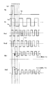
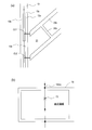
- FIG. 5 is a diagram illustrating an example of voltage waveforms and timings of signals for driving the liquid crystal display device illustrated in FIG. 4. It is a figure for demonstrating the structure of the pixel of LCD100 of embodiment by this invention, (a) is a top view which shows the structure of one pixel of LCD100, (b) is formed in 1st board
- FIG. 6C is a plan view showing a continuous opening pattern 20, and FIG. 5C is a plan view showing a dielectric protrusion pattern 44 formed on the second substrate 100 ⁇ / b> B.
- FIG. 7 is a plan view showing a continuous opening pattern 20 formed on a first substrate 110A used in place of the first substrate 100A of the LCD 100 shown in FIG. 6. It is a figure for demonstrating the structure of the pixel of LCD120 of other embodiment by this invention, (a) is a top view which shows the structure of one pixel of LCD120, (b) is formed in 1st board
- FIG. 6C is a plan view showing the continuous opening pattern 20 formed, and FIG.
- FIG. 5C is a plan view showing the dielectric protrusion pattern 44 formed on the second substrate 120B.
- FIG. 6 is a diagram for explaining a pixel structure of an LCD according to still another embodiment of the present invention, wherein (a) is a plan view showing the structure of one pixel of the LCD 130, and (b) is a diagram illustrating the first substrate 130A. It is a top view which shows the continuous opening pattern 20 formed, (c) is a top view which shows the dielectric protrusion pattern 44 formed in the 2nd board
- FIG. 6C is a plan view showing a continuous opening pattern 20 formed on the substrate
- FIG. 5C is a plan view showing a dielectric protrusion pattern 44 formed on the second substrate 200B.
- (a) is a top view which shows the structure of one pixel of LCD210
- (b) is 1st board
- FIG. 6C is a plan view showing a continuous opening pattern 20 formed on the substrate
- FIG. 5C is a plan view showing a dielectric protrusion pattern 44 formed on the second substrate 210B.
- FIG. 14 is a diagram for explaining a pixel structure of an LCD 220 according to still another embodiment of the present invention, (a) is a plan view showing a structure of two pixels of the LCD 220, and (b) is a first substrate 220A.
- FIG. 4C is a plan view showing a continuous opening pattern 20 formed on the substrate, and FIG. 4C is a plan view showing a dielectric protrusion pattern 44 formed on the second substrate 220B. It is a top view which shows the continuous opening pattern 20 formed in the 1st board
- FIG. 14 is a plan view showing a dielectric protrusion pattern 44 in an LCD 240 in which the second substrate 220B of the LCD 220 shown in FIG. 13 is changed.
- (A)-(d) is a top view for demonstrating the variation of a linear connection part.
- FIG. 10 is a diagram for explaining a pixel structure of an LCD 250 according to still another embodiment of the present invention, (a) is a plan view showing a structure of two pixels of the LCD 250, and (b) is a first substrate 250A.
- FIG. 4C is a plan view showing a continuous opening pattern 20 formed on the substrate, and FIG. 4C is a plan view showing a dielectric protrusion pattern 44 formed on the second substrate 250B.
- FIG. 18 is a plan view showing first electrodes 21a and 21b in an LCD 260 in which the first substrate 250A of the LCD 250 shown in FIG. 17 is changed.
- FIG. FIG. 14 is a diagram for explaining the structure of a pixel of an LCD 300 according to still another embodiment of the present invention, wherein (a) is a plan view showing the structure of two pixels of the LCD 300, and (b) is a first substrate 300A.
- FIG. 6C is a plan view showing a continuous opening pattern 20 formed on the substrate, and FIG. 5C is a plan view showing a dielectric protrusion pattern 44 formed on the second substrate 300B.
- FIG. 1 is a top view which shows the structure of two pixels of LCD310, and the continuous opening pattern 20 and opening pattern 42 is a plan view showing a dielectric protrusion pattern 44 formed on the second substrate 310B.
- FIG. It is a figure for demonstrating the structure of the pixel of LCD320 of further another embodiment by this invention, and is a top view which shows the dielectric protrusion pattern 44.
- FIG. It is a figure for demonstrating the structure of the pixel of LCD330 of further another embodiment by this invention, (a) is a top view which shows the continuous opening pattern 20 and the dielectric protrusion pattern 44, (b) It is a top view which shows the continuous opening pattern 20.
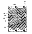
- FIG. It is a figure for demonstrating the structure of the pixel of LCD340 of further another embodiment by this invention, and is a top view which shows the continuous opening pattern 20 and the dielectric protrusion pattern 44.
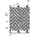
- FIG. It is a figure for demonstrating the structure of the pixel of LCD350 of further another embodiment by this invention, and is a top view which shows the continuous opening pattern 20 and the dielectric protrusion pattern 44.
- FIG. It is a figure for demonstrating the structure of the pixel of LCD360 of further another embodiment by this invention, (a) is a top view which shows the continuous opening pattern 20 and the dielectric protrusion pattern 44, (b) is continuous. It is a top view which shows the opening pattern 20 which was made.
- FIG. 14 is a diagram for explaining a pixel structure of an LCD 380 according to still another embodiment of the present invention, in which (a) is a plan view showing a continuous opening pattern 20 and a dielectric protrusion pattern 44, and (b) is a first diagram. It is a top view which shows the continuous opening pattern 20 which 1 substrate 380A has.
- the LCDs 10 ⁇ / b> A and 10 ⁇ / b> B include a first electrode 21 formed on the first substrate, a second electrode 41 formed on the second substrate facing the first electrode 21, and between the first electrode 21 and the second electrode 41.
- the vertical alignment type liquid crystal layer 33 aligns liquid crystal molecules 33a having negative dielectric anisotropy substantially perpendicular to the surfaces of the first electrode 21 and the second electrode 41 (for example, 87 ° or more and 90 ° or less) when no voltage is applied. It is a thing. Typically, it is obtained by providing a vertical alignment film (not shown) on the surface of each of the first electrode 21 and the second electrode 41 on the liquid crystal layer 33 side.
- a dielectric protrusion (rib) or the like is provided as a domain restricting structure, the liquid crystal molecules 33a are aligned substantially perpendicular to the surface on the liquid crystal layer side such as the dielectric protrusion.
- a first domain restriction structure 22 is provided on the first electrode 21 side of the liquid crystal layer 33, and a second domain restriction structure (opening 42 or dielectric protrusion 44) is provided on the second electrode 41 side of the liquid crystal layer 33. Is provided.
- the liquid crystal molecules 33a receive the alignment restricting force from the first domain restricting structure and the second domain restricting structure and receive the first electrode.
- a voltage is applied between the first electrode 21 and the second electrode 41, it falls (tilts) in the direction indicated by the arrow in the figure. That is, since the liquid crystal molecules 33a tilt in a uniform direction in each liquid crystal region, each liquid crystal region can be regarded as a domain.
- the first domain restriction structure and the second domain restriction structure (these may be collectively referred to as “domain restriction structure”) are provided in a straight line (band shape) in each pixel, as shown in FIG. (a) And (b) is sectional drawing in the direction orthogonal to the extending direction of a linear domain control structure. Liquid crystal domains that are different from each other by 180 ° in the direction in which the liquid crystal molecules 33a fall are formed on both sides of each domain regulating structure.
- the LCD 10A shown in FIG. 1A has an opening (slit) 22 formed in the first electrode 21 as a first domain restricting structure, and on the liquid crystal layer 33 side of the second electrode 41 as a second domain restricting structure.
- the dielectric protrusion 44 is formed, and the opening 22 and the dielectric protrusion 44 are each extended in a straight line (strip shape).
- the dielectric protrusion 44 functions to align the liquid crystal molecules 33a in a direction perpendicular to the extending direction of the dielectric protrusions 44 by aligning the liquid crystal molecules 33a substantially perpendicular to the side surface 41a.
- the opening 22 generates an oblique electric field in the liquid crystal layer 33 near the edge of the opening 22 when a potential difference is formed between the first electrode 21 and the second electrode 41, and the opening 22 extends. It acts to align the liquid crystal molecules 33a in a direction perpendicular to the direction.
- the opening 22 and the dielectric protrusion 44 are arranged in parallel to each other with a certain distance therebetween, and a liquid crystal domain is formed between the opening 22 and the dielectric protrusion 44 adjacent to each other.
- FIG. 1B is different from the LCD 10A of FIG. 1A in that the LCD 10B shown in FIG. 1B has an opening 22 and an opening 42 as a first domain restriction structure and a second domain restriction structure, respectively.
- the opening 22 and the opening 42 generate an oblique electric field in the liquid crystal layer 33 near the edges of the openings 22 and 42 when a potential difference is formed between the first electrode 21 and the second electrode 41.
- the liquid crystal molecules 33a are aligned in a direction orthogonal to the extending direction of the openings 22 and 42.
- the opening 22 and the opening 42 are arranged in parallel to each other with a certain distance therebetween, and a liquid crystal domain is formed between them.
- the first electrode 21 is a pixel electrode (also a subpixel electrode), and the second electrode 41 is a counter electrode.
- the first domain regulating structure is the opening 22 formed in the first electrode 21, and the second domain regulating structure is formed on the dielectric protrusion 44 or the counter electrode 42 formed on the liquid crystal layer 33 side of the counter electrode 41.
- the opening 42 is made.
- the first domain restriction structure has a first linear component extending in the first direction and a second linear component extending in a second direction that is approximately 90 ° different from the first direction
- the second domain regulating structure has a third linear component (parallel to the first linear component) extending in the first direction and a fourth linear component (parallel to the second linear component) extending in the second direction
- at least one of the second linear component or the third and fourth linear components is present, and the first linear component and the third linear component are alternately arranged when viewed from the normal direction of the first substrate.
- the second linear component and the fourth linear component are alternately arranged.
- FIGS. 2A and 2B are schematic plan views showing examples of the arrangement of liquid crystal domains in one pixel of the MVA type LCD according to the embodiment of the present invention, and FIG. 2A is a normal pixel.
- FIG. 2B schematically shows the arrangement of liquid crystal domains in a pixel having a multi-pixel structure.
- PP indicates the polarization axis of the polarizing plate on the back side (backlight side)
- PA indicates the polarization axis of the polarizing plate on the viewer side.
- the directions in which the liquid crystal molecules are tilted when a voltage is applied to the liquid crystal layer differ from each other by about 90 °.
- Four domains A, B, C and D are formed in one pixel P.
- four liquid crystal domains A, B, C and D are formed in one pixel P, and each subpixel SP1 and SP2 has a director. Only a pair of liquid crystal domains whose orientation directions are different from each other by 180 ° may be formed.
- the first and second domain regulating structures may be arranged so that four liquid crystal domains A to D are formed in each sub-pixel.
- each pixel P may have two or more liquid crystal domains A to D.
- 3 (a) and 3 (b) are plan views schematically showing the structure of a pixel, where (a) shows a normal pixel and (b) shows the structure of a pixel having a multi-pixel structure. In either case, the second electrode (counter electrode) 41 is omitted.
- a normal pixel P is defined by a first electrode (pixel electrode) 21.
- the first electrode 21 is electrically connected to the source bus line 13 via the TFT 14 connected to the gate bus line 12.
- a CS capacitor is formed in parallel with the liquid crystal capacitor formed by the first electrode 21, the liquid crystal layer, and the second electrode. One of the CS capacitors is connected to the first electrode 21, and the other is connected to the CS bus line 15.
- the pixel P having a multi-pixel structure is divided into a sub-pixel SP1 and a sub-pixel SP2 as shown in FIG.
- Corresponding TFTs 14a and 14b and auxiliary capacitors CS1 and CS2 are connected to the first pixel electrodes (subpixel electrodes) 21a and 21b constituting the subpixels SP1 and SP2, respectively.
- the gate electrodes of the TFTs 14 a and 14 b are connected to a common gate bus line (scanning line) 12, and the source electrodes of the TFTs 14 a and 14 b are connected to a common (identical) source bus line (signal line) 13.
- the auxiliary capacitors CS1 and CS2 are connected to the corresponding CS bus line (auxiliary capacitor line) 15a and CS bus line 15b, respectively.
- the auxiliary capacitors CS1 and CS2 are formed between the auxiliary capacitor electrode electrically connected to the first electrodes 21a and 21b and the auxiliary capacitor counter electrode electrically connected to the CS bus lines 15a and 15b, respectively.
- the insulating layer (not shown, for example, a gate insulating film) is formed.
- the auxiliary capacitor counter electrodes of the auxiliary capacitors CS1 and CS2 are independent from each other, and have a structure in which different auxiliary capacitor counter voltages (also referred to as “CS signals”) can be supplied from the CS bus lines 15a and 15b, respectively. .
- the voltages of the auxiliary capacitor counter electrodes of the auxiliary capacitors CS1 and CS2 that is, , The voltage supplied from the CS bus line 15a or the CS bus line 15b) (by the direction and magnitude of the change) are changed to be applied to the liquid crystal capacitors of the respective subpixels SP1 and SP2.
- a state in which the effective voltage differs that is, a state in which the luminance is different is obtained.
- a display signal voltage can be supplied from one source bus line 13 to the two subpixels SP1 and SP2, so that the number of subbuses and source drivers can be increased without increasing the number of source bus lines and the number of source drivers.
- the brightness of the pixels SP1 and SP2 can be made different from each other.
- the sub-pixel SP1 displays with a luminance higher than that of the sub-pixel SP2 for a given display signal voltage.
- the sub-pixel SP1 it is not necessary for the sub-pixel SP1 to display with higher luminance than the sub-pixel SP2 with respect to all display signal voltages (gradation display signals), and with higher luminance than at least one halftone display signal voltage. Show it.
- the subpixel SP1 performs display with a luminance higher than that of the subpixel SP2.
- the luminance order may be changed for each frame, for example.
- FIG. 4 is a diagram showing an equivalent circuit of an LCD having a multi-pixel structure
- FIG. 5 is a diagram showing an example of voltage waveforms and timings of signals for driving the LCD shown in FIG.
- Vg is a gate voltage
- Vs is a source voltage
- Vcs1 and Vcs2 are voltages of auxiliary capacitors of the subpixel SP1 and the subpixel SP2
- Vlc1 and Vlc2 are voltages of the pixel electrodes of the subpixel SP1 and the subpixel SP2, respectively.
- Vsp is given to the source voltage as a positive polarity with respect to the median value Vsc of the source voltage.
- a signal obtained by amplifying the voltage with the amplitude voltage Vad and shifting the phases of CS1 and CS2 by 180 degrees is input to CS1 and CS2.
- Vg changes from VgL to VgH
- the TFTs of both subpixels are turned on, and the subpixel SP1, subpixel SP2, and auxiliary capacitors CS1, CS2 are charged with the voltage Vsp.
- Vg changes from VgH to VgL, the TFTs of both subpixels are turned off, and the subpixel SP1, subpixel SP2 and auxiliary capacitors CS1, CS2 are electrically insulated from the source bus line.
- Vlc2 Vsp ⁇ Vdd It becomes.
- Vcs1 Vcom ⁇ Vad
- Vcs2 Vcom + Vad It is.
- Vcs1 of the auxiliary capacitance bus line CS1 changes from Vcom ⁇ Vad to Vcom + Vad
- Vcs2 changes, from Vcom + Vad to Vcom ⁇ Vad
- Vlc2 Vsp-Vdd-2 ⁇ K ⁇ Vad It becomes.
- K Ccs / (Clc (V) + Ccs). “ ⁇ ” Indicates multiplication.
- Vcs1 changes from Vcom + Vad to Vcom ⁇ Vad
- Vcs2 changes from Vcom ⁇ Vad to Vcom + Vad.
- Vlc2 Vsp ⁇ Vdd It becomes.
- Vcs1 changes from Vcom ⁇ Vad to Vcom + Vad
- Vcs2 changes from Vcom + Vad to Vcom ⁇ Vad
- Vlc2 Vsp-Vdd-2 ⁇ K ⁇ Vad It becomes.
- V2 Vsp ⁇ Vdd ⁇ K ⁇ Vad ⁇ Vcom Therefore, the subpixel SP1 is a bright subpixel, and the subpixel SP2 is a dark subpixel.
- FIG. 6A is a plan view showing the structure of one pixel of the LCD 100
- FIG. 6B is a plan view showing a continuous opening pattern 20 formed on the first substrate (TFT substrate) 100A
- FIG. 6C is a plan view showing the dielectric protrusion pattern 44 formed on the second substrate (counter substrate) 100B. 6 and 8 to 28 reflect the aspect ratio of the actual LCD pixel.
- the LCD 100 has normal pixels (not having a multi-pixel structure). As shown in FIG. 6A, it has a gate bus line 12, a source bus line 13, a TFT 14, a CS bus line 15, a drain lead wiring 16, a contact hole 17 and a CS counter electrode 18.
- the electrical configuration of the LCD 100 is the same as that in FIG.
- the first electrode 21 has an opening 22 as a first domain regulating structure.
- the opening 22 has four first linear components 22a (45 ° downward) and four second linear components 22b (45 ° downward).
- one first linear component 22 a and one second linear component 22 b are directly connected to form a V-shaped opening 23.
- the four first linear components 22a are connected to each other by a linear connection opening 24a extending in a direction different from the first linear component 22a by about 90 °
- the four second linear components 22b are connected to the second linear component 22a. They are connected to each other by a linear connection opening 24b extending in a direction different from that of 22b by about 90 °.
- the linear connection openings 24a and 24b generate an electric field that disturbs the alignment of liquid crystal molecules in the liquid crystal domain, and therefore preferably have a width smaller than the widths of the first linear component 22a and the second linear component 22b. . In this way, all the openings formed in the first electrode 21 are connected to form one continuous opening pattern 20.
- the opening pattern 20 has line symmetry with a line parallel to the gate bus line 12 (or CS bus line 15) as an axis of symmetry.
- a notch 21t having a side parallel to the V-shaped opening 23 is formed on the left edge near the center in the column direction of the first electrode 21, and the orientation of the liquid crystal molecules near the notch 21t is adjusted. Stabilize.
- the second substrate 100B has a dielectric protrusion pattern 44 as a second domain regulating structure on the liquid crystal layer side of the second electrode 41.
- the dielectric protrusion pattern 44 includes five third linear components 44a (lower 45 ° to the right) parallel to the first linear component 22a, and five fourth linear components 44b (lower 45 ° to the left) parallel to the second linear component 22b. ).
- the two third linear components 44 a and the two fourth linear components 44 b are directly connected to form two V-shaped dielectric protrusions 45.
- the five third linear components 44a and the five fourth linear components 44b are arranged in parallel and alternately with the four first linear components 22a and the four second linear components 22b. Between these, four types of liquid crystal domains (see FIG. 2A) are formed.
- openings (first linear component and second linear component) functioning as the first domain restriction structure formed in first electrode 21 are part of a continuous opening pattern.
- the opening pattern 20 is continuous, the end portions of the two first linear components 22a that are adjacent to each other and exist in the vicinity of the edge of the first electrode 21, A small region is separated from the first electrode 21 by cutting the end of the second linear component 22b or the end of the first linear component 22a and the end of the second linear component 22b to the edge of the first electrode 21. I can do it.
- FIG. 7 (a) when cutting from the ends of the two second linear components 22b adjacent to each other to the edge of the first electrode 21 along the cutting lines CL1 and CL2, two second linear components are obtained. 22b, the straight connection opening 24b, the cutting lines CL1 and CL2, and the portion surrounded by the edge of the first electrode 21 are separated from the first electrode 21 and are electrically independent from the first electrode 21. Therefore, when a conductive foreign substance exists in this portion and a short circuit occurs between the first electrode 21 and the second electrode 41, the short circuit is repaired by cutting along the cutting lines CL1 and CL2.
- FIG. 7A illustration of the first electrodes 21 of pixels adjacent in the row direction is omitted for simplicity.
- the LCD 100 has an advantage that it can be repaired with a few cut points as compared with the conventional configuration that does not have the linear connection openings 24a and 24b.
- a portion smaller than the conventional one can be selected and electrically separated, there is an advantage that the area that can be used after the repair can be made larger than the conventional one.
- the portion including the contact hole 17 for electrically connecting the first electrode 21 and the drain of the TFT 14 is separated, it does not function as the first electrode 21.
- a branch structure that can be cut independently of each other is provided in the wiring that electrically connects each contact hole and the drain of the TFT.
- Such a structure is disclosed in Japanese Patent Laid-Open No. 2002-55361 (for example, FIG. 4).
- the entire content disclosed in JP-A-2002-55361 is incorporated herein by reference.
- a ladder is formed like the source bus line 13 shown in FIG. It is preferable to adopt a structure.
- the source bus line 13 shown in FIG. 7A is provided with two parallel main lines 13a and 13b and a plurality of branch lines 13d connecting the two parallel main lines 13a and 13b to each other.
- An opening 13 c is formed in the bus line 13.
- Such a ladder structure is disclosed in WO 07/34596. The entire disclosure of WO 07/34596 is hereby incorporated by reference for reference.
- the redundant wiring 19 may be provided as shown in FIG.
- the redundant wiring 19 is connected at two points indicated by ⁇ , so that the source bus line 13 (m) is displayed from the opposite direction.
- a signal voltage can be supplied.
- a configuration having such redundant wiring is disclosed in Japanese Patent Laid-Open No. 2008-197583.
- the entire disclosure of Japanese Patent Application Laid-Open No. 2008-197583 is incorporated herein by reference.
- FIG. 8 is a plan view showing a continuous opening pattern 20 formed on the first substrate 110A used in place of the first substrate 100A of the LCD 100 shown in FIG.
- the continuous opening pattern 20 of the first electrode 21 included in the first substrate 110A is in addition to the continuous opening pattern 20 of the first electrode 21 of the first substrate 100A, and further, the first linear component 22a or the second linear component. It further has a plurality of fine openings 25a and 25b parallel to a direction substantially orthogonal to 22b.
- the fine openings 25a and 25b have a width smaller than the width of the first linear component 22a or the second linear component 22b.
- the fine openings 25a and 25b have a width of 2 ⁇ m to 4 ⁇ m and 2 ⁇ m to 2 ⁇ m, respectively. They are arranged in parallel to each other with an interval of 4 ⁇ m.
- the fine opening 25a is formed in the vicinity of the linear connection openings 24a and 24b, and acts to stabilize the alignment of liquid crystal molecules in the vicinity of the linear connection openings 24a and 24b.
- the liquid crystal molecules between the two fine openings 25a adjacent to each other are equally affected by the oblique electric field from the two fine openings 25a and the oblique electric field from the first linear component 22a or the second linear component 22b. Under the influence, it is oriented parallel to the extending direction of the fine opening 25a.
- the fine opening 25a extends in the direction orthogonal to the first linear component 22a or the second linear component 22b. However, it may be deviated from the orthogonal relationship within a range in which the above-described effect can be obtained.
- the fine opening 25b is formed near the edge of the first electrode 21, and acts to stabilize the alignment of liquid crystal molecules in the vicinity of the edge of the first electrode 21 in the same manner as the fine opening 25a.
- the fine opening 25b is provided only on the side where the first linear component 22a or the second linear component 22b and the edge of the first electrode 21 form an acute angle, but the first linear component 22a or the second linear component. 22b and the edge of the 1st electrode 21 may be provided in the side which makes an obtuse angle, and you may provide in both.
- the fine openings 25 a and 25 b are included in the continuous opening pattern 20.
- the fine openings 25 a and 25 b are not necessarily included in the continuous opening pattern 20, but are preferably connected to the continuous opening pattern 20. This is because the orientation of the liquid crystal molecules is easily stabilized under the influence of the oblique electric field from the first linear component 22a or the second linear component 22b.
- FIG. 9A is a plan view showing the structure of one pixel of the LCD 120
- FIG. 9B is a plan view showing a continuous opening pattern 20 formed on the first substrate 120A
- c) is a plan view showing a dielectric protrusion pattern 44 formed on the second substrate 120B.
- the pixels of the LCD 120 are normal pixels as with the LCD 100.
- the first electrode 21 of the LCD 120 includes a V-shaped opening 23 in which the continuous opening pattern 20 includes both the first linear component 22a and the second linear component 22b.
- the pixel is a rectangle having a long side in the column direction.
- the six V-shaped openings 23 are arranged so that an axis parallel to the long side is an axis of symmetry.
- the continuous opening pattern 20 of the first electrode 21 includes a plurality of V-shaped openings 23, and further includes a linear opening 24 that extends in a direction that equally divides the angle inside the V-shaped openings 23. .
- the linear opening 24 is parallel to the long side of the first electrode 21.
- the linear opening 24 is connected to the center of the plurality of V-shaped openings 23.
- the continuous opening pattern 20 of the first electrode 21 further has a fine opening 25 a formed near the center of the V-shaped opening 23, and the fine opening 25 a is near the center of the V-shaped opening 23. It acts to stabilize the orientation of the liquid crystal molecules. Further, the continuous opening pattern 20 has a fine opening 25b formed near the edge of the first electrode 21, and the fine opening 25b stabilizes the alignment of liquid crystal molecules in the vicinity of the edge of the first electrode 21. Act on.
- a dielectric protrusion pattern 44 as a second domain restricting structure is formed on the liquid crystal layer side of the second electrode 41.
- the dielectric protrusion pattern 44 has seven third linear components 44a (lower 45 °) and seven fourth linear components 44b (lower 45 °). Of these, the six third linear components 44 a and the six fourth linear components 44 b are directly connected to form six V-shaped dielectric protrusions 45. As shown in FIG. 9C, the seven third linear components 44a and the seven fourth linear components 44b are arranged in parallel and alternately with the six first linear components 22a and the six second linear components 22b. Between these, four types of liquid crystal domains (see FIG. 2A) are formed.
- the liquid crystal in the pixel has a rectangular shape
- the V-shaped opening 23 and the V-shaped dielectric protrusion 45 are arranged so that the axis parallel to the long side is the axis of symmetry
- the liquid crystal in the pixel The molecular orientation can be controlled efficiently. That is, it is easier to divide the V-shaped opening 23 and the V-shaped dielectric protrusion 45 evenly into smaller regions than arranging them so that the axis parallel to the short side is the axis of symmetry.
- FIG. 10A is a plan view showing the structure of one pixel of the LCD 130
- FIG. 10B is a plan view showing a continuous opening pattern 20 formed on the first substrate 130A
- c) is a plan view showing a dielectric protrusion pattern 44 formed on the second substrate 130B.
- the pixel of the LCD 130 is also a normal pixel, but has two first electrodes 21a and 21b as shown in FIG.
- the first electrodes 21a and 21b are both connected to the drain of one TFT 14 through contact holes 17a and 17b, are supplied with the same voltage, and the CS bus line 15 is also common to the two first electrodes 21a and 21b. It is not a multi-pixel structure.
- the continuous opening pattern 20 of the first electrode 21a has the first linear component 22a, but does not have the second linear component 22b.
- the continuous opening pattern 20 of the first electrode 21b has a second linear component 22b, but does not have the first linear component 22a, contrary to the continuous opening pattern 20 of the first electrode 21a.
- the continuous opening pattern 20 of the first electrode 21a has four first linear components 22a, which are connected to the first linear components 22a by linear connection openings 24a extending in a direction different from the first linear component 22a by about 90 °.
- the continuous opening pattern 20 of the first electrode 21b has four second linear components 22b, which are connected to each other by a linear connection opening 24b extending in a direction different from the second linear component 22b by about 90 °.
- Each continuous opening pattern 20 has a fine opening 25a formed near the linear connection opening 24 and a fine opening 25b formed near the edges of the first electrodes 21a and 21b.
- a triangular notch is formed between the first electrode 21a and the first electrode 21b, which stabilizes the alignment of liquid crystal molecules in the same manner as the notch 21t shown in FIG. 6B. It works to let you. This notch may be omitted.
- the dielectric protrusion pattern 44 in the region corresponding to the first electrode 21a has five third linear components 44a
- the dielectric protrusion pattern in the region corresponding to the first electrode 21b. 44 has five fourth linear components 44b.
- the five third linear components 44a and the five fourth linear components 44b are arranged in parallel and alternately with the four first linear components 22a and the four second linear components 22b. Between these, four types of liquid crystal domains (see FIG. 2A) are formed. Note that the positions of the opening pattern 22 and the dielectric protrusion pattern 44 are slightly shifted between adjacent pixels.
- FIG. 11A is a plan view showing the structure of one pixel of the LCD 200
- FIG. 11B is a plan view showing a continuous opening pattern 20 formed on the first substrate 200A
- c) is a plan view showing a dielectric protrusion pattern 44 formed on the second substrate 200B.
- the pixels of the LCD 200 have a multi-pixel structure. As shown in FIG. 11A, two first electrodes 21a and 21b are provided and connected to a common source bus line 13 via corresponding TFTs 14a and 14b, respectively.
- the TFTs 14a and 14b are ON / OFF controlled by a common gate bus line 12 disposed between the first electrode 21a and the second electrode 21b.
- the first electrodes 21a and 21b are connected to the drains of the corresponding TFTs 14a and 14b in the contact holes 17a and 17b, respectively.
- the CS bus lines 15a and 15b are independent from each other, and form a CS capacitor between the CS counter electrodes 18a and 18b, respectively.
- the pixels of the LCD 200 are represented by the equivalent circuit shown in FIG. 4, and can be driven by the method described with reference to FIG.
- a columnar spacer (also referred to as a photo spacer) 49 is disposed on the gate bus line 12 disposed between the first electrode 21a and the first electrode 21b.
- the first electrode 21a has two first linear components 22a and two second linear components 22b, and a pair of them has a V-shaped opening 23. Forming.
- the two first linear components 22a are connected to each other through the linear connection opening 24a, and the two second linear components 22b are connected to each other through the linear connection opening 24b.
- it has the fine opening part 25b formed in the edge vicinity of the 1st electrodes 21a and 21b.
- the first electrodes 21a and 21b are arranged symmetrically with respect to the gate bus line 12, and the continuous opening pattern 20 of the two first electrodes 21a and 21b has a line-symmetric relationship with the gate bus line 12 as the axis of symmetry. is there.
- the columnar spacer 49 disturbs the alignment of liquid crystal molecules in the vicinity thereof, the influence on the display can be reduced by disposing the columnar spacer 49 on the gate bus line 12 generally formed of a light-shielding material. Further, by arranging the first electrodes 21a and 21b having a line-symmetric structure, the influence on the display can be made uniform.
- the dielectric protrusion pattern 44 also has line symmetry with respect to the gate bus line 12.
- the dielectric protrusion pattern 44 in the region corresponding to the first electrode 21a has three third linear components 44a, and the dielectric protrusion pattern 44 in the region corresponding to the first electrode 21b has three fourth linear components 44b. have.
- the dielectric protrusion pattern 44 has a linear dielectric protrusion 46 extending from the V-shaped tip of the V-shaped dielectric protrusion 45 to the dominant angle side.
- the linear dielectric protrusion 46 acts to stabilize the alignment of liquid crystal molecules in the vicinity of the V-shaped tip of the V-shaped dielectric protrusion 45.
- the three third linear components 44a and the three fourth linear components 44b are arranged in parallel and alternately with the two first linear components 22a and the two second linear components 22b. Between these, four types of liquid crystal domains (see FIG. 2A) are formed.
- FIG. 12A is a plan view showing the structure of one pixel of the LCD 210
- FIG. 12B is a plan view showing a continuous opening pattern 20 formed on the first substrate 210A
- c) is a plan view showing a dielectric protrusion pattern 44 formed on the second substrate 210B.
- the pixels of the LCD 210 have a multi-pixel structure similar to the pixels of the LCD 200, are represented by the equivalent circuit shown in FIG. 4, and can be driven by the method described with reference to FIG.
- the two CS bus lines 15a and 15b are arranged so as to cross the vicinity of the respective centers of the first electrodes 21a and 21b.
- the first electrode 21a has two first linear components 22a and two second linear components 22b, and a pair of them has a V-shaped opening 23a.
- the V-shaped opening 23a has a flat tip.
- the two first linear components 22a are connected to each other through the linear connection opening 24a, and the two second linear components 22b are connected to each other through the linear connection opening 24b.
- it has the fine opening part 25b formed in the edge vicinity of the 1st electrodes 21a and 21b.
- the first electrodes 21a and 21b are arranged symmetrically with respect to the gate bus line 12, and the continuous opening pattern of the two first electrodes 21a and 21b is in a line-symmetric relationship with the gate bus line 12 as the axis of symmetry. .
- Each continuous opening pattern 20 has line symmetry with the corresponding CS bus line 15a or 15b as an axis of symmetry.
- the dielectric protrusion pattern 44 also has line symmetry with respect to the gate bus line 12.
- the dielectric protrusion pattern 44 in the region corresponding to the first electrode 21 a has two V-shaped dielectric protrusions 45.
- the V-shaped dielectric protrusion 45 on the left side in FIG. 12C has an angle from the horizontal direction between the fourth linear component 44b and the third linear component 44a relative to the fourth linear component 44b.
- a large linear portion 44d is provided, and a linear portion 44c having a larger angle from the horizontal direction than the fourth linear component 44b is provided between the third linear component 44a and the fourth linear component 44b.
- the columnar spacer 49 is formed on the gate bus line 12 and is formed integrally with the dielectric protrusion pattern 44.
- the influence on display can be reduced by disposing the columnar spacer 49 on the gate bus line 12 that is generally formed of a light-shielding material. Further, by arranging the first electrodes 21a and 21b having a line-symmetric structure, the influence on the display can be made uniform.
- FIG. 13A is a plan view showing the structure of two pixels of the LCD 220
- FIG. 13B is a plan view showing a continuous opening pattern 20 formed on the first substrate 220A.
- the LCD 220 has a multi-pixel structure similar to the pixel of the LCD 210, is represented by the equivalent circuit shown in FIG. 4, and can be driven by the method described with reference to FIG.
- the two CS bus lines 15a and 15b are arranged so as to cross the vicinity of the respective centers of the first electrodes 21a and 21b.
- the first electrode 21a has two first linear components 22a and two second linear components 22b, which are directly connected to each other, and has two V-shaped openings. Part 23 is formed.
- the pixel is a rectangle having a long side in the column direction, and the two V-shaped openings 23 included in the first electrode 21a are arranged so that an axis parallel to the long side is an axis of symmetry.
- the two V-shaped openings 23 are connected to each other by linear openings 24 that extend in a direction that equally divides the angle inside the two V-shaped openings 23.
- the linear opening 24 is connected to the center of the two V-shaped openings 23.
- the first electrodes 21a and 21b are arranged symmetrically with respect to the gate bus line 12, and the continuous opening pattern 20 of the two first electrodes 21a and 21b has a line-symmetric relationship with the gate bus line 12 as the axis of symmetry. is there.
- the V-shaped openings 23 of the two first electrodes 21 a and 21 b are arranged with the upper side (the wider one) of the V shape facing the gate bus line 12.
- the V shape, the virtual extension line extending in the direction in which the V shape extends from the V shape, and the gate bus line 12 form an isosceles triangle with the bent portion of the V shape as a vertex.
- the apex angles of these two isosceles triangles are right angles and form a square.
- fine openings 25a, 25b and 25c are connected to the V-shaped opening 23.
- the fine opening 25 a is formed in the vicinity of the linear connection opening 24 and acts to stabilize the alignment of liquid crystal molecules in the vicinity of the linear connection opening 24.
- the fine opening 25b is formed near the edge of the first electrode 21 and acts to stabilize the alignment of liquid crystal molecules in the vicinity of the edge of the first electrode 21 in the same manner as the fine opening 25a.
- the fine opening 25c is formed on the dominant angle side from the V-shaped tip of the V-shaped opening 23 so as to stabilize the alignment of liquid crystal molecules in the vicinity of the V-shaped tip of the V-shaped opening 23. Works.
- the fine opening 25c has the same function as the linear dielectric protrusion 46 included in the dielectric protrusion pattern 44 shown in FIG. Further, since the fine opening 25c is located near the edges of the first electrodes 21a and 21b, it also acts to stabilize the alignment of the liquid crystal molecules near the edges.
- the dielectric protrusion pattern 44 has a V-shaped dielectric protrusion including a third linear component 44a (lower 45 °) and a fourth linear component 44b (lower 45 °). 45.
- the V-shaped dielectric protrusion 45 is disposed between two V-shaped openings 23, and four types of liquid crystal domains (see FIG. 2 (a)) therebetween. ).
- the contact holes 17a and 17b can be freely arranged.
- the advantage is that the degree can be increased.
- the degree of freedom of arrangement of the columnar spacers 49 can be increased. As shown in FIG. 13C, the alignment of the liquid crystal molecules in the vicinity of the columnar spacer 49 is stabilized by matching the shape of the columnar spacer 49 with the dielectric protrusion pattern 44 when viewed from the direction perpendicular to the substrate. Can be made.
- FIG. 14 shows a continuous opening pattern 20 formed on the first substrate 230A used in place of the first substrate 220A of the LCD 220 shown in FIG.
- the continuous opening pattern 20 shown in FIG. 14 has fine openings on the inner side (subordinate side) of the V-shaped side closer to the gate bus line 12 in the two V-shaped openings 23 arranged in the column direction. 25d is formed.
- the fine opening portion 25d acts to stabilize the alignment of the liquid crystal molecules inside the V-shaped opening portion 23.
- FIG. 15 shows a dielectric protrusion pattern 44 in the LCD 240 obtained by changing the second substrate 220B of the LCD 220 shown in FIG.
- the dielectric protrusion pattern 44 of the LCD 240 has a linear dielectric protrusion 46 positioned inside the V-shaped opening on the side close to the gate bus line 12 in addition to the V-shaped dielectric protrusion 45. Yes.
- This linear dielectric protrusion 46 acts to stabilize the alignment of the liquid crystal molecules inside the V-shaped opening 23, similarly to the fine opening 25 d shown in FIG. 14.
- FIG. 16 (a) to 16 (d) show examples of variations of the connecting portion that connects the V-shaped opening 23.
- a part of the fine opening 25c formed on the dominant angle side from the V-shaped tip of the lower V-shaped opening 23 is the upper V-shaped. It is connected to one of the fine openings 25a formed inside the opening 23 via a straight connection opening 24r.
- the linear connection opening 24s extending from the V-shaped tip of the lower V-shaped opening 23 to the dominant angle side is the upper V-shaped opening 23. Is connected to one of the fine openings 25a formed on the inner side of the.
- the tip of the fine opening 25c formed on the dominant angle side from the tip of the V-shape of the lower V-shaped opening 23 is the upper V-shape. Is connected to the center of the opening 23 via a linear connection opening 24t.
- the linear connection opening 24u formed on the dominant angle side from the V-shaped tip of the lower V-shaped opening 23 has an upper V-shaped opening. It is connected to one of the fine openings 25 a formed inside the opening 23. A part of the fine opening 25c formed on the dominant angle side of the tip of the lower V-shaped opening 23 is connected to the linear connection opening 24u.
- FIG. 17A is a plan view showing the structure of two pixels of the LCD 250
- FIG. 17B is a plan view showing a continuous opening pattern 20 formed on the first substrate 250A
- c) is a plan view showing a dielectric protrusion pattern 44 formed on the second substrate.
- the LCD 250 has a multi-pixel structure like the pixels of the LCD 210, and is represented by the equivalent circuit shown in FIG. 4, and can be driven by the method described with reference to FIG.
- the two CS bus lines 15a and 15b are arranged so as to cross the vicinity of the respective centers of the first electrodes 21a and 21b.
- the first electrode 21a has one first linear component 22a and one second linear component 22b, which are directly connected to each other, and has one V-shaped opening. Part 23 is formed.
- the pixel is a rectangle having a long side in the column direction, and one V-shaped opening 23 included in the first electrode 21a is arranged so that an axis parallel to the short side is an axis of symmetry. Fine openings 25 b and 25 c are connected to the V-shaped opening 23.
- a notch 21t having a side parallel to the V-shaped opening 23 is formed on the left edge near the center in the column direction of the first electrodes 21a and 21b, and the liquid crystal molecules in the vicinity of the notch 21t are formed. Stabilize the orientation.
- the first electrodes 21a and 21b are arranged symmetrically with respect to the gate bus line 12, and the continuous opening pattern 20 of the two first electrodes 21a and 21b has a line-symmetric relationship with the gate bus line 12 as the axis of symmetry. is there.
- the portion of the dielectric protrusion pattern 44 corresponding to the first electrode 21a includes two third linear components 44a (45 ° downward) and two fourth linear components 44b (left). 45 degrees). A pair of them is directly connected to form one V-shaped dielectric protrusion 45.
- two third linear components 44a and two fourth linear components 44b are arranged in parallel and alternately with one first linear component 22a and one second linear component 22b. Between these, four types of liquid crystal domains (see FIG. 2A) are formed.
- the columnar spacer 49 is formed on the gate bus line 12 and overlaps the V-shaped tip of the V-shaped dielectric protrusion 45. (Integrally).
- the shapes of the first electrodes 21a and 21b in the LCD 260 obtained by changing the first substrate 250A of the LCD 250 shown in FIG. 17 will be described.
- the first electrodes 21a and 21b of the LCD 260 shown in FIG. 18 have a notch 21t at the left edge near the center in the column direction of the first electrode 21a.
- the notch 21t has a side parallel to the V-shaped opening 23 to act to stabilize the alignment of liquid crystal molecules in the vicinity of the notch 21t, but may be omitted in this way.
- FIG. 19A is a plan view showing the structure of two pixels of the LCD 300
- FIG. 19B is a plan view showing a continuous opening pattern 20 formed on the first substrate 300A
- FIG. 4 is a plan view showing a dielectric protrusion pattern 44 formed on the second substrate 300B.
- the LCD 300 has three first electrodes 21a, 21b and 21c and two TFTs 14a and 14b in one pixel.
- the drain of the TFT 14a is connected to the first electrodes 21a and 21c through contact holes 18a and 18c, respectively.
- the drain of the TFT 14b is connected to the first electrode 21b through a contact hole 18b.
- the pixel of the LCD 300 has three first electrodes 21a, 21b, and 21c, but the first electrodes 21a and 21c are equivalent, and are substantially represented by the equivalent circuit shown in FIG. It can be driven in the manner described with reference.
- a subpixel including the first electrodes 21a and 21c is a dark subpixel
- a subpixel including the first electrode 21b is a bright subpixel.
- the continuous opening pattern 20 of the first electrode 21b has three V-shaped openings 23 each including both the first linear component 22a and the second linear component 22b.
- the three V-shaped openings 23 are arranged so that an axis parallel to the long side of the pixel is an axis of symmetry.
- a fine opening 25a and a fine opening 25b are connected to each of the V-shaped openings 23.
- the three V-shaped openings 23 are connected by a linear opening 24 that extends in a direction that equally bisects the angle inside the V-shaped opening 23.
- the linear opening 24 is connected to the center of the V-shaped opening 23.
- the continuous opening pattern 20 of the first electrode 21b has a fine opening 25a formed near the linear connection opening 24 and a fine opening 25b formed near the edge of the first electrode 21b. Further, in the lowermost V-shaped opening 23, a fine opening 25d is formed inside the V-shape (inferior angle side).
- the continuous opening pattern 20 of the first electrode 21a has the first linear component 22a but does not have the second linear component 22b.
- the continuous opening pattern 20 of the first electrode 21c has the second linear component 22b, but does not have the first linear component 22a, contrary to the continuous opening pattern 20 of the first electrode 21a.
- the continuous opening pattern 20 of the first electrode 21a has four first linear components 22a, which are connected to the first linear components 22a by linear connection openings 24a extending in a direction different from the first linear component 22a by about 90 °.
- the continuous opening pattern 20 of the first electrode 21c has four second linear components 22b, which are connected to each other by a linear connection opening 24b extending in a direction different from the first linear component 22b by about 90 °.
- Each continuous opening pattern 20 has a fine opening 25b formed near the edges of the first electrodes 21a and 21c.
- the dielectric protrusion pattern 44 in the region corresponding to the first electrode 21b has four third linear components 44a and four fourth linear components 44b. Also, three of these pairs are directly connected to form three V-shaped dielectric protrusions 45.
- the four third linear components 44a and the four fourth linear components 44b are arranged in parallel and alternately with the three first linear components 22a and the third second linear components 22b, and there are four types of liquid crystal domains between them. (See FIG. 2A).
- the dielectric protrusion pattern 44 in the region corresponding to the first electrode 21a has five third linear components 44a
- the dielectric protrusion pattern 44 in the region corresponding to the first electrode 21c has five fourth straight lines. It has component 44b.
- the five third linear components 44a and the five fourth linear components 44b are arranged in parallel and alternately with the four first linear components 22a and the four second linear components 22b, and there are four types of liquid crystal domains between them. (See FIG. 2A).
- FIG. 20A is a plan view showing the structure of two pixels of the LCD 310, which is a plan view showing a continuous opening pattern 20 and an opening pattern 42
- FIG. 20B is a diagram showing a dielectric formed on the second substrate 310B
- 5 is a plan view showing a body protrusion pattern 44.
- the LCD 310 has an opening pattern 42 instead of the dielectric protrusion pattern 44 formed on the second substrate of the LCD 300.
- the opening pattern 42 includes a third linear component 42a and a fourth linear component 42b, and a V-shaped opening 43 formed by connecting them directly.
- the opening pattern 42 formed on the second electrode 41 of the second substrate 310B of the LCD 310 has a linear opening 47 extending from the V-shaped tip of the lowermost V-shaped opening 43 to the dominant angle side. Have. This is because the V-shaped opening 23 has a V-shaped opening 23 instead of the fine opening 25d formed on the inner side (recessed angle side) of the V-shaped opening 23 on the lowermost side of the LCD 300. It acts to stabilize the orientation of the inner liquid crystal molecules.
- the continuous opening pattern 20 included in the first substrate of the LCD 310 is a fine opening formed on the inner side (subordinate side) of the V shape of the V-shaped opening 23 at the lowermost side of the continuous opening pattern 20 of the LCD 300. It is the same except that the portion 25d is not provided.
- FIG. 21 is a plan view showing the dielectric protrusion pattern 44 of the LCD 320.
- the dielectric protrusion pattern 44 has the same pattern as the opening pattern 42 formed in the second electrode 41 shown in FIG.
- the dielectric protrusion pattern and the opening pattern as the second domain regulating structure formed on the second substrate are equivalent, and any of them can be adopted.
- FIG. 22A is a plan view showing the continuous opening pattern 20 and the dielectric protrusion pattern 44
- FIG. 22B is a plan view showing the continuous opening pattern 20 formed on the first substrate 330A. is there.
- the continuous opening pattern 20 of the LCD 330 corresponds to a pattern in which the fine opening portions 25a and 25d of the continuous opening pattern 20 of the LCD 300 shown in FIG. 19 are omitted.
- the dielectric projection pattern 44 of the LCD 300 is a linear dielectric projection 46 that extends from the V-shaped tip of the lowermost V-shaped dielectric projection 45 to the dominant angle side. have.
- FIG. 23 is a plan view showing the continuous opening pattern 20 and the dielectric protrusion pattern 44 of the LCD 340.
- the continuous opening pattern 20 of the LCD 340 is the same as the continuous opening pattern 20 of the LCD 330 shown in FIG.
- the dielectric protrusion pattern 44 included in the LCD 340 has linear dielectric protrusions 46 extending from the V-shaped end portions of all the V-shaped dielectric protrusions 45 to the dominant angle side. is doing.
- FIG. 24 is a plan view showing the continuous opening pattern 20 and the dielectric protrusion pattern 44 of the LCD 350.
- the continuous opening pattern 20 included in the LCD 350 is the same as the continuous opening pattern 20 of the LCD 330 shown in FIG.
- the dielectric protrusion pattern 44 of the LCD 350 is the same as the dielectric protrusion pattern of the LCD 300B shown in FIG.
- the fine openings 25a, 25c, 25d and the linear dielectric protrusion 46 for stabilizing the alignment of the liquid crystal molecules in the vicinity of the V-shaped opening 23 and the V-shaped dielectric protrusion 45 are omitted. You may do it.
- FIG. 25A is a plan view showing the continuous opening pattern 20 and the dielectric protrusion pattern 44
- FIG. 25B is a plan view showing the continuous opening pattern 20.
- the linear dielectric protrusions 46 extending from the V-shaped tip portions of all the V-shaped dielectric protrusions 45 to the dominant angle side are provided as in the dielectric protrusion pattern of the LCD 340 shown in FIG.
- the two linear dielectric protrusions 46 overlap the linear connection opening 24. Since the alignment of the liquid crystal molecules by the linear dielectric protrusions 46 and the alignment of the liquid crystal molecules by the linear connection openings 24 do not match, the alignment disorder of the liquid crystal molecules in this region may increase.
- the LCD 360 shown in FIG. 25 has the same dielectric protrusion pattern 44 as the LCD 340 shown in FIG. 23, but the shape of the connection opening 24c of the continuous opening pattern 20 is different from the linear connection opening 24 of the LCD 340. That is, the connection opening 24c included in the continuous opening pattern 20 of the LCD 360 is bent so as not to overlap the linear dielectric protrusion 46 formed at the corresponding position.
- the above-mentioned alignment disorder of the liquid crystal molecules can be suppressed.
- FIG. 26A is a plan view showing the continuous opening pattern 20 and the dielectric protrusion pattern 44
- FIG. 26B is a plan view showing the continuous opening pattern 20.
- the dielectric projection pattern 44 included in the LCD 370 is the same as the dielectric projection pattern 44 of the LCD 350 shown in FIG. 24, and does not have the linear dielectric projection 46 extending from the V-shaped tip to the dominant angle side.
- the continuous opening pattern 20 included in the first electrodes 21a and 21c of the LCD 370 is the same as the continuous opening pattern 20 included in the LCD 350 illustrated in FIG.
- the continuous opening pattern 20 included in the first electrode 21b of the LCD 370 is a continuous opening pattern included in the first electrode 21b of the LCD 350 in that the V-shaped opening 23 is divided at one location of the first linear component 22a. It is different from the pattern 20. Of the first linear component 22a, a portion separated from the V-shaped opening 23 is shown as a linear component 22e.
- the continuous opening pattern 20 included in the first electrode 21b of the LCD 370 does not have the linear connection opening 24 connected to the center of the V-shaped opening 23, and two adjacent first linear components 22a. And a linear connection opening 24b for connecting two adjacent second linear components 22b.
- the V-shaped opening 23 has a fine opening 25c on the dominant angle side of the tip, and the V-shaped opening 23 has a fine opening 25d on the inner side (subordinate angle side).
- FIG. 27A is a plan view showing the continuous opening pattern 20 and the dielectric protrusion pattern 44
- FIG. 27B is a plan view showing the continuous opening pattern 20 included in the first substrate 380A.
- the dielectric protrusion pattern 44 of the LCD 380 is the same as the dielectric protrusion pattern 44 of the LCD 350 shown in FIG. 24, and does not have the linear dielectric protrusion 46 extending from the V-shaped tip to the dominant angle side.
- the continuous opening pattern 20 included in the first electrodes 21a and 21c of the LCD 380 is different from the continuous opening pattern 20 included in the LCD 350 illustrated in FIG. 24 in that the fine opening 25b is not included.
- the continuous opening pattern 20 included in the first electrode 21b of the LCD 380 has a fine opening 25e connected to the linear connection opening 24, and a fine opening on the dominant angle side of the tip of the V-shaped opening 23. 24 and the continuous opening pattern 20 of the first electrode 21b of the LCD 350 shown in FIG. 24 in that it has a fine opening 25d on the inferior angle side of the tip of the V-shaped opening 23. Is different.
- FIG. 28A is a plan view showing the continuous opening pattern 20 and the dielectric protrusion pattern 44
- FIG. 28B is a plan view showing the continuous opening pattern 20 included in the first substrate 390A.
- the continuous opening pattern 20 of the first electrodes 21a and 21c of the LCD 390 is the same as the continuous opening pattern 20 of the first electrodes 21a and 21c of the LCD 380 shown in FIG. 27, and the continuous opening pattern of the first electrode 21b. 20 and different.
- the continuous opening pattern 20 of the first electrode 21b of the LCD 390 has three first linear components 22a and three second linear components 22b. Two of these pairs are directly connected to each other to form two V-shaped openings 23.
- the pixel is a rectangle having a long side in the column direction, and the two V-shaped openings 23 are arranged so that an axis parallel to the short side is an axis of symmetry. Note that the second linear component 22b that forms one V-shaped opening 23 is divided into two parts.
- the continuous opening pattern 20 of the first electrode 21b of the LCD 390 does not have the linear connection opening 24 connected to the center of the V-shaped opening 23, and connects two adjacent first linear components 22a. It has the linear connection opening part 24a and the linear connection opening part 24b which connects two adjacent 2nd linear components 22b.
- the V-shaped opening 23 has a fine opening 25e on the dominant angle side of the tip, and the V-shaped opening 23 has a fine opening 25d on the inner side (subordinate angle side).
- each of the first electrodes 21, 21 a, 21 b, 21 c has a continuous opening (continuous opening pattern 20).
- continuous opening pattern 20 As described above, in the MVA type LCD according to the embodiment of the present invention, each of the first electrodes 21, 21 a, 21 b, 21 c has a continuous opening (continuous opening pattern 20).
- continuous opening pattern 20 As described above, in the MVA type LCD according to the embodiment of the present invention, each of the first electrodes 21, 21 a, 21 b, 21 c has a continuous opening (continuous opening pattern 20).
- continuous opening pattern 20 As described above, in the MVA type LCD according to the embodiment of the present invention, each of the first electrodes 21, 21 a, 21 b, 21 c has a continuous opening (continuous opening pattern 20).
- the linear dielectric protrusion 46 (linear opening 47) may be provided, or the fine openings 25a, 25c, 25d, and 25e may be provided.
- the fine openings 25a and the like have a two-dimensional expansion, there is an advantage that alignment errors are less likely to occur than when the linear dielectric protrusions 46 (linear openings 47) are provided.
- the present invention is applied to an MVA type liquid crystal display device.
Landscapes
- Physics & Mathematics (AREA)
- Nonlinear Science (AREA)
- Mathematical Physics (AREA)
- Chemical & Material Sciences (AREA)
- Crystallography & Structural Chemistry (AREA)
- General Physics & Mathematics (AREA)
- Optics & Photonics (AREA)
- Spectroscopy & Molecular Physics (AREA)
- Geometry (AREA)
- Liquid Crystal (AREA)
Abstract
Description
Vlc1=Vsp-Vdb
Vlc2=Vsp-Vdd
となる。
Vcs1=Vcom-Vad
Vcs2=Vcom+Vad
である。
Vlc1=Vsp-Vdb+2・K・Vad
Vlc2=Vsp-Vdd-2・K・Vad
となる。ただし、K=Ccs/(Clc(V)+Ccs)である。「・」は乗算を示す。
Vlc1=Vsp-Vdb
Vlc2=Vsp-Vdd
となる。
Vlc1=Vsp-Vdb+2・K・Vad
Vlc2=Vsp-Vdd-2・K・Vad
となる。
Vlc1=Vsp-Vdb+K・Vad
Vlc2=Vsp-Vdd-K・Vad
となる。
V1=Vsp-Vdb+K・Vad-Vcom
V2=Vsp-Vdd-K・Vad-Vcom
となるため、副画素SP1が明副画素、副画素SP2が暗副画素となる。
13 ソースバスライン
14 TFT
15 CSバスライン
16 ドレイン引き出し配線
17 コンタクトホール
18 CS対向電極
20 連続した開口パターン
21 第1電極(画素電極)
22 開口部
22a 第1直線成分
22b 第2直線成分
23 V字状の開口部
24 直線状連結開口部
41 第2電極(対向電極)
42 第2電極が有する開口パターン
43 V字状の開口部
44 誘電体突起パターン
44a 第3直線成分
44b 第4直線成分
45 V字状の誘電体突起
Claims (19)
- 第1基板と、第2基板と、前記第1基板と前記第2基板との間に設けられた垂直配向型の液晶層と、前記第1基板に形成された第1ドメイン規制構造と、前記第2基板に形成された第2ドメイン規制構造とを有し、
前記第1ドメイン規制構造は、第1方向に延びる第1直線成分と、前記第1方向と略90°異なる第2方向に延びる第2直線成分とを有し、
前記第2ドメイン規制構造は、前記第1方向に延びる第3直線成分と、前記第2方向に延びる第4直線成分とを有し、
前記第1および第2直線成分または前記第3および第4直線成分の少なくとも一方は複数存在し、前記第1基板の法線方向から見たときに、前記第1直線成分と前記第3直線成分とは交互に配置されており、且つ、前記第2直線成分と前記第4直線成分とは交互に配置されており、任意の画素の前記液晶層に電圧が印加されたときに、前記第1直線成分と前記第3直線成分との間および前記第2直線成分と前記第4直線成分との間に、液晶分子が倒れる方位が互いに約90°異なる4つのドメインを形成するMVA型の液晶表示装置であって、
任意の画素は、前記第1基板に形成された少なくとも1つの第1電極と、前記第2基板に形成された第2電極とを有し、前記少なくとも1つの第1電極のそれぞれは連続した開口パターンを有し、前記第1ドメイン規制構造の前記第1および第2直線成分は、前記少なくとも1つの第1電極のそれぞれが有する前記連続した開口パターンのいずれかに含まれている、液晶表示装置。 - 前記少なくとも1つの第1電極は、前記連続した開口パターンが前記第1および第2直線成分の両方を含むV字状の開口部を含む、第1のタイプの第1電極を含む、請求項1に記載の液晶表示装置。
- 前記第1のタイプの第1電極の前記連続した開口パターンは、前記第1および第2直線成分の両方を複数個ずつ含み、前記V字状の開口部を複数個含む、請求項2に記載の液晶表示装置。
- 前記第1のタイプの第1電極の前記連続した開口パターンは、前記V字状の開口部の内側の角度をニ等分する方向に延びる直線状開口部をさらに含む、請求項3に記載の液晶表示装置。
- 前記第1のタイプの第1電極は、長辺および短辺を有し、前記直線状開口部は前記長辺に平行である、請求項4に記載の液晶表示装置。
- 前記直線状開口部は、複数の前記V字状の開口部の中央に連結している、請求項5に記載の液晶表示装置。
- 前記少なくとも1つの第1電極は、前記第1直線成分または前記第2直線成分に略直交する方向に平行な複数の微細開口部をさらに有する、請求項2から6のいずれかに記載の液晶表示装置。
- 前記複数の微細開口部は前記V字状の開口部の中央付近に形成されている、請求項7に記載の液晶表示装置。
- 前記複数の微細開口部は前記少なくとも1つの第1電極のエッジ付近に形成されている、請求項7または8に記載の液晶表示装置。
- 前記複数の微細開口部は、前記連続した開口パターンに含まれる、請求項7から9のいずれかに記載の液晶表示装置。
- 前記少なくとも1つの第1電極は、複数の第1電極であって、
前記複数の第1電極は、前記連続した開口パターンが、前記第1直線成分または前記第2直線成分の一方だけを含む第2のタイプの第1電極と、前記第1直線成分または前記第2直線成分の他方だけを含む第3のタイプの第1電極とを含む、請求項1から10のいずれかに記載の液晶表示装置。 - 前記第2のタイプの第1電極の前記連続した開口パターンは、前記第1直線成分または前記第2直線成分を複数個含み、かつ、前記複数の前記第1直線成分または前記複数の前記第2直線成分は、それぞれ、前記第1方向と約90°異なる方向に延びる直線状連結開口部、または、前記第2方向と約90°異なる方向に延びる直線状連結開口部によって連結されている、請求項11に記載の液晶表示装置。
- 前記複数の第1電極は、ゲートバスラインまたはCSバスラインに関して対称に配置された2つの第1電極を含み、
前記2つの第1電極の前記連続した開口パターンは、前記ゲートバスラインまたは前記CSバスラインを対称軸とする線対称の関係にある、請求項1から12のいずれかに記載の液晶表示装置。 - 前記2つの第1電極はいずれも、前記連続した開口パターンが前記第1および第2直線成分の両方を含むV字状の開口部を含む、第1のタイプの第1電極であって、前記V字状の開口部はV字の上側を前記ゲートバスラインまたは前記CSバスラインに向けて配置されている、請求項13に記載の液晶表示装置。
- 前記少なくとも1つの第1電極のそれぞれが有する連続した開口パターンは、前記少なくとも1つの第1電極のエッジと交わっていない、請求項1から14のいずれかに記載の液晶表示装置。
- 前記第1基板の法線方向から見たとき、前記少なくとも1つの第1電極のそれぞれのエッジはソースバスラインと部分的に重なっている、請求項1から15のいずれかに記載の液晶表示装置。
- 前記第2ドメイン規制構造は、前記第2電極に形成された開口パターンまたは前記第2電極の前記液晶層側に形成された誘電体突起パターンに含まれる、請求項1から16のいずれかに記載の液晶表示装置。
- 前記少なくとも1つの第1電極は、前記連続した開口パターンが前記第1および第2直線成分の両方を含むV字状の開口部を含み、
前記第1基板の法線方向から見たとき、前記第2電極の前記開口パターンまたは前記誘電体突起パターンは、前記V字状の開口部の内側の角度をニ等分する方向に延びる直線状開口部または直線状誘電体突起をさらに含む、請求項17に記載の液晶表示装置。 - 前記少なくとも1つの第1電極は、前記第1基板の法線方向から見たとき、前記V字状の開口部の内側の角度をニ等分する方向に延びる、前記第2電極の前記直線状開口部または前記直線状誘電体突起と平行で、且つ、前記第2電極の前記直線状開口部または前記直線状誘電体突起と重なる開口部を有しない、請求項18に記載の液晶表示装置。
Priority Applications (6)
| Application Number | Priority Date | Filing Date | Title |
|---|---|---|---|
| JP2011507037A JP5307230B2 (ja) | 2009-04-03 | 2010-04-01 | 液晶表示装置 |
| EP10758296A EP2416213A4 (en) | 2009-04-03 | 2010-04-01 | LIQUID CRYSTAL DISPLAY DEVICE |
| RU2011144576/28A RU2011144576A (ru) | 2009-04-03 | 2010-04-01 | Жидкокристаллическое устройство отображения |
| US13/259,845 US20120019757A1 (en) | 2009-04-03 | 2010-04-01 | Liquid crystal display device |
| CN2010800141813A CN102365577A (zh) | 2009-04-03 | 2010-04-01 | 液晶显示装置 |
| BRPI1014702A BRPI1014702A2 (pt) | 2009-04-03 | 2010-04-01 | dispositivo de vídeo de cristal líquido. |
Applications Claiming Priority (2)
| Application Number | Priority Date | Filing Date | Title |
|---|---|---|---|
| JP2009091130 | 2009-04-03 | ||
| JP2009-091130 | 2009-04-03 |
Publications (1)
| Publication Number | Publication Date |
|---|---|
| WO2010113517A1 true WO2010113517A1 (ja) | 2010-10-07 |
Family
ID=42827824
Family Applications (1)
| Application Number | Title | Priority Date | Filing Date |
|---|---|---|---|
| PCT/JP2010/002404 Ceased WO2010113517A1 (ja) | 2009-04-03 | 2010-04-01 | 液晶表示装置 |
Country Status (7)
| Country | Link |
|---|---|
| US (1) | US20120019757A1 (ja) |
| EP (1) | EP2416213A4 (ja) |
| JP (1) | JP5307230B2 (ja) |
| CN (1) | CN102365577A (ja) |
| BR (1) | BRPI1014702A2 (ja) |
| RU (1) | RU2011144576A (ja) |
| WO (1) | WO2010113517A1 (ja) |
Cited By (1)
| Publication number | Priority date | Publication date | Assignee | Title |
|---|---|---|---|---|
| CN103926715A (zh) * | 2013-11-18 | 2014-07-16 | 上海中航光电子有限公司 | 像素单元、像素阵列结构及显示装置 |
Families Citing this family (1)
| Publication number | Priority date | Publication date | Assignee | Title |
|---|---|---|---|---|
| CN104570443B (zh) * | 2014-12-30 | 2017-07-28 | 深圳市华星光电技术有限公司 | 像素阵列结构和液晶显示面板 |
Citations (6)
| Publication number | Priority date | Publication date | Assignee | Title |
|---|---|---|---|---|
| JP2002365636A (ja) * | 1997-06-12 | 2002-12-18 | Fujitsu Ltd | 液晶表示装置 |
| JP2004093654A (ja) * | 2002-08-29 | 2004-03-25 | Sanyo Electric Co Ltd | 液晶表示器及びその製造方法 |
| JP2006106101A (ja) * | 2004-09-30 | 2006-04-20 | Sanyo Electric Co Ltd | 液晶表示パネル |
| JP2006259719A (ja) * | 2005-02-24 | 2006-09-28 | Samsung Electronics Co Ltd | アレイ基板、その製造方法、及びこれを具備した表示パネル |
| WO2007034596A1 (ja) * | 2005-09-22 | 2007-03-29 | Sharp Kabushiki Kaisha | アクティブマトリクス基板、表示装置、テレビジョン装置、アクティブマトリクス基板の製造方法、及び表示装置の製造方法 |
| WO2008078441A1 (ja) * | 2006-12-25 | 2008-07-03 | Sharp Kabushiki Kaisha | 液晶表示パネル、液晶表示素子、及び、液晶表示装置 |
Family Cites Families (9)
| Publication number | Priority date | Publication date | Assignee | Title |
|---|---|---|---|---|
| JP3398025B2 (ja) * | 1997-10-01 | 2003-04-21 | 三洋電機株式会社 | 液晶表示装置 |
| US7301595B2 (en) * | 1997-10-01 | 2007-11-27 | Sanyo Electric Co., Ltd. | Vertically aligned liquid crystal display |
| JP3957430B2 (ja) * | 1998-09-18 | 2007-08-15 | シャープ株式会社 | 液晶表示装置 |
| JP4397444B2 (ja) * | 1998-12-28 | 2010-01-13 | シャープ株式会社 | 液晶表示装置 |
| JP2004301878A (ja) * | 2003-03-28 | 2004-10-28 | Fujitsu Display Technologies Corp | 液晶表示装置 |
| JP2005055880A (ja) * | 2003-07-24 | 2005-03-03 | Sharp Corp | 液晶表示装置およびその駆動方法 |
| TWI280437B (en) * | 2004-07-29 | 2007-05-01 | Au Optronics Corp | Thin film transistor array |
| EP2261729B1 (en) * | 2005-10-18 | 2014-05-07 | Semiconductor Energy Laboratory Co, Ltd. | Liquid crystal display device and electronic apparatus |
| EP2144111A4 (en) * | 2007-05-08 | 2011-03-30 | Sharp Kk | ACTIVE MATRIX SUBSTRATE, LIQUID CRYSTAL PANEL, LIQUID CRYSTAL DISPLAY UNIT, LIQUID CRYSTAL DISPLAY DEVICE, AND TELEVISION RECEIVER |
-
2010
- 2010-04-01 US US13/259,845 patent/US20120019757A1/en not_active Abandoned
- 2010-04-01 CN CN2010800141813A patent/CN102365577A/zh active Pending
- 2010-04-01 EP EP10758296A patent/EP2416213A4/en not_active Withdrawn
- 2010-04-01 RU RU2011144576/28A patent/RU2011144576A/ru not_active Application Discontinuation
- 2010-04-01 BR BRPI1014702A patent/BRPI1014702A2/pt not_active IP Right Cessation
- 2010-04-01 JP JP2011507037A patent/JP5307230B2/ja not_active Expired - Fee Related
- 2010-04-01 WO PCT/JP2010/002404 patent/WO2010113517A1/ja not_active Ceased
Patent Citations (6)
| Publication number | Priority date | Publication date | Assignee | Title |
|---|---|---|---|---|
| JP2002365636A (ja) * | 1997-06-12 | 2002-12-18 | Fujitsu Ltd | 液晶表示装置 |
| JP2004093654A (ja) * | 2002-08-29 | 2004-03-25 | Sanyo Electric Co Ltd | 液晶表示器及びその製造方法 |
| JP2006106101A (ja) * | 2004-09-30 | 2006-04-20 | Sanyo Electric Co Ltd | 液晶表示パネル |
| JP2006259719A (ja) * | 2005-02-24 | 2006-09-28 | Samsung Electronics Co Ltd | アレイ基板、その製造方法、及びこれを具備した表示パネル |
| WO2007034596A1 (ja) * | 2005-09-22 | 2007-03-29 | Sharp Kabushiki Kaisha | アクティブマトリクス基板、表示装置、テレビジョン装置、アクティブマトリクス基板の製造方法、及び表示装置の製造方法 |
| WO2008078441A1 (ja) * | 2006-12-25 | 2008-07-03 | Sharp Kabushiki Kaisha | 液晶表示パネル、液晶表示素子、及び、液晶表示装置 |
Non-Patent Citations (1)
| Title |
|---|
| See also references of EP2416213A4 * |
Cited By (2)
| Publication number | Priority date | Publication date | Assignee | Title |
|---|---|---|---|---|
| CN103926715A (zh) * | 2013-11-18 | 2014-07-16 | 上海中航光电子有限公司 | 像素单元、像素阵列结构及显示装置 |
| CN103926715B (zh) * | 2013-11-18 | 2016-08-31 | 上海中航光电子有限公司 | 像素单元、像素阵列结构及显示装置 |
Also Published As
| Publication number | Publication date |
|---|---|
| US20120019757A1 (en) | 2012-01-26 |
| JP5307230B2 (ja) | 2013-10-02 |
| EP2416213A4 (en) | 2012-10-31 |
| BRPI1014702A2 (pt) | 2016-04-12 |
| CN102365577A (zh) | 2012-02-29 |
| EP2416213A1 (en) | 2012-02-08 |
| RU2011144576A (ru) | 2013-05-10 |
| JPWO2010113517A1 (ja) | 2012-10-04 |
Similar Documents
| Publication | Publication Date | Title |
|---|---|---|
| US10520781B2 (en) | Liquid crystal display | |
| KR101006202B1 (ko) | 수평 전계형 액정 표시 장치용 픽셀 구조체 | |
| JP5802319B2 (ja) | 液晶表示装置 | |
| KR101366459B1 (ko) | 액정 표시 장치 | |
| EP2466369B1 (en) | Liquid crystal display to increase side view visibility | |
| US20150015822A1 (en) | Liquid crystal display | |
| WO2009130908A1 (ja) | 液晶表示装置 | |
| KR101404874B1 (ko) | 액티브 매트릭스 기판 및 액정 표시 장치 | |
| JP5173025B2 (ja) | 液晶表示装置 | |
| KR102256463B1 (ko) | 액정 표시 장치 | |
| JP5173026B2 (ja) | 液晶表示装置 | |
| JP5307230B2 (ja) | 液晶表示装置 | |
| JP5443619B2 (ja) | アクティブマトリクス基板および表示装置 | |
| JP5378511B2 (ja) | 液晶表示装置 | |
| WO2011078173A1 (ja) | 液晶表示装置 |
Legal Events
| Date | Code | Title | Description |
|---|---|---|---|
| WWE | Wipo information: entry into national phase |
Ref document number: 201080014181.3 Country of ref document: CN |
|
| 121 | Ep: the epo has been informed by wipo that ep was designated in this application |
Ref document number: 10758296 Country of ref document: EP Kind code of ref document: A1 |
|
| WWE | Wipo information: entry into national phase |
Ref document number: 13259845 Country of ref document: US |
|
| WWE | Wipo information: entry into national phase |
Ref document number: 2011507037 Country of ref document: JP |
|
| WWE | Wipo information: entry into national phase |
Ref document number: 4080/KOLNP/2011 Country of ref document: IN |
|
| NENP | Non-entry into the national phase |
Ref country code: DE |
|
| WWE | Wipo information: entry into national phase |
Ref document number: 2010758296 Country of ref document: EP |
|
| ENP | Entry into the national phase |
Ref document number: 2011144576 Country of ref document: RU Kind code of ref document: A |
|
| REG | Reference to national code |
Ref country code: BR Ref legal event code: B01A Ref document number: PI1014702 Country of ref document: BR |
|
| ENP | Entry into the national phase |
Ref document number: PI1014702 Country of ref document: BR Kind code of ref document: A2 Effective date: 20110929 |