WO2010123052A1 - 発光装置 - Google Patents
発光装置 Download PDFInfo
- Publication number
- WO2010123052A1 WO2010123052A1 PCT/JP2010/057120 JP2010057120W WO2010123052A1 WO 2010123052 A1 WO2010123052 A1 WO 2010123052A1 JP 2010057120 W JP2010057120 W JP 2010057120W WO 2010123052 A1 WO2010123052 A1 WO 2010123052A1
- Authority
- WO
- WIPO (PCT)
- Prior art keywords
- light
- phosphor
- wavelength conversion
- recess
- emitting device
- Prior art date
- Legal status (The legal status is an assumption and is not a legal conclusion. Google has not performed a legal analysis and makes no representation as to the accuracy of the status listed.)
- Ceased
Links
Images


Classifications
-
- H—ELECTRICITY
- H10—SEMICONDUCTOR DEVICES; ELECTRIC SOLID-STATE DEVICES NOT OTHERWISE PROVIDED FOR
- H10H—INORGANIC LIGHT-EMITTING SEMICONDUCTOR DEVICES HAVING POTENTIAL BARRIERS
- H10H20/00—Individual inorganic light-emitting semiconductor devices having potential barriers, e.g. light-emitting diodes [LED]
- H10H20/80—Constructional details
- H10H20/85—Packages
- H10H20/851—Wavelength conversion means
- H10H20/8514—Wavelength conversion means characterised by their shape, e.g. plate or foil
-
- H—ELECTRICITY
- H10—SEMICONDUCTOR DEVICES; ELECTRIC SOLID-STATE DEVICES NOT OTHERWISE PROVIDED FOR
- H10H—INORGANIC LIGHT-EMITTING SEMICONDUCTOR DEVICES HAVING POTENTIAL BARRIERS
- H10H20/00—Individual inorganic light-emitting semiconductor devices having potential barriers, e.g. light-emitting diodes [LED]
- H10H20/80—Constructional details
- H10H20/85—Packages
- H10H20/851—Wavelength conversion means
- H10H20/8515—Wavelength conversion means not being in contact with the bodies
-
- H—ELECTRICITY
- H10—SEMICONDUCTOR DEVICES; ELECTRIC SOLID-STATE DEVICES NOT OTHERWISE PROVIDED FOR
- H10H—INORGANIC LIGHT-EMITTING SEMICONDUCTOR DEVICES HAVING POTENTIAL BARRIERS
- H10H20/00—Individual inorganic light-emitting semiconductor devices having potential barriers, e.g. light-emitting diodes [LED]
- H10H20/80—Constructional details
- H10H20/85—Packages
- H10H20/858—Means for heat extraction or cooling
- H10H20/8583—Means for heat extraction or cooling not being in contact with the bodies
Definitions
- the present invention relates to an LED light-emitting device that emits light emitted from an LED element after wavelength conversion by a phosphor layer.
- Patent Document 1 Conventionally, light emission that emits light of a color different from that of LED elements such as white by combining LED elements that emit blue light or ultraviolet light with various phosphors using a gallium nitride compound semiconductor An apparatus has been developed (Patent Document 1).
- Such a light emitting device using an LED element has advantages such as small size, power saving and long life, and is widely used as a light source for display and a light source for illumination.
- LED elements with high output and high brightness have been developed, and their uses are increasing more and more.
- the present invention has been made in view of such problems, and has been made for the first time by focusing attention on the heat generated by a phosphor that has been neglected in the past.
- the heat of a wavelength conversion member containing the phosphor It is a main aim of the present invention to provide an LED light-emitting device that can efficiently emit light.
- the light-emitting device includes a base body having a recess opening in the upper end surface, an LED element mounted on the bottom surface of the recess, a translucent member that seals the LED element, and a phosphor. And a wavelength converting member placed on the translucent member, and a translucent heat radiating member placed on the wavelength converting member and covering the opening of the recess.
- the said translucent heat radiating member since the said translucent heat radiating member is mounted on the said wavelength conversion member, it can discharge
- the wavelength conversion member is formed by arranging fluorescent regions emitting different colors of light in parallel.
- the LED element When the light emitting device according to the present invention emits white light, the LED element emits near-ultraviolet light in order to suppress uneven color tone, and the phosphor emits red light.
- the phosphor hereinafter referred to as red phosphor
- the phosphor emitting green light hereinafter referred to as green phosphor
- the phosphor emitting blue light hereinafter referred to as blue phosphor
- the translucent heat radiating member and the wavelength converting member may be opposite in the vertical direction, and such a light emitting device is also one aspect of the present invention.
- the light-emitting device according to the present invention having such an aspect includes a base having a recess opening in the upper end surface, an LED element mounted on the bottom surface of the recess, and a translucent member that seals the LED element. And a light transmissive heat radiating member placed on the light transmissive member, and a wavelength conversion member containing a phosphor placed on the light transmissive heat radiating member and covering the opening of the recess. And.
- the light emitting device 1 includes a base body 2 having a recess 22 that opens on an upper end surface 21, an LED element 3 mounted on a bottom surface 221 of the recess 22, and an LED element 3.
- the member 6 is provided.
- the base 2 has a recess 22 that opens to the upper end surface 21.
- a base 2 is formed by molding an insulating material having high thermal conductivity such as alumina or aluminum nitride.
- the base body 2 mounts an LED element 3 to be described later on the bottom surface 221 of the recess 22, and a wiring conductor (not shown) for electrically connecting the LED element 3 to the bottom surface 221. Is formed.
- This wiring conductor is led to the outer surface of the light emitting device 1 through a wiring layer (not shown) formed inside the base 2 and connected to the external electric circuit board, whereby the LED element 3 and the external electric circuit board are connected. Are electrically connected.
- a step portion 23 is formed on the side wall of the concave portion 22 of the base body 2, and an edge portion of a translucent heat radiating member 6 described later is placed on the upper end surface of the step portion 23.
- the LED element 3 is formed, for example, by laminating a gallium nitride compound semiconductor in the order of an n-type layer, a light emitting layer, and a p-type layer on a sapphire substrate. Such an LED element 3 emits blue light or ultraviolet light. .
- the LED element 3 is flip-chip mounted on the bottom surface 221 of the recess 22 using solder bumps, gold bumps, etc. with the gallium nitride compound semiconductor facing down (the bottom surface 221 side of the recess 22).
- the translucent member 4 is filled in the concave portion 22 and seals the LED element 3.
- the translucent member 4 is made of a silicone resin having excellent translucency and heat resistance and having a small difference in refractive index from the LED element 3. It is.
- the wavelength conversion member 5 contains a phosphor 51 inside and is placed on the translucent member 4.
- Examples of such a wavelength conversion member 5 include those in which the phosphor 51 is dispersed in a silicone resin that is excellent in translucency and heat resistance and has a small refractive index difference from the translucent member 4.
- the concave portion 22 may be filled with an uncured silicone resin in which the phosphor 51 is dispersed, or a sheet processed into a predetermined size may be used. .
- the phosphor 51 contained in the wavelength conversion member 5 is not particularly limited, and examples thereof include a red phosphor, a green phosphor, a blue phosphor, and a yellow phosphor.
- the translucent heat radiating member 6 is for releasing the heat of the wavelength conversion member 5 and is placed on the wavelength conversion member 5 to cover the opening of the recess 22.
- Examples of such translucent heat radiating member 6 include those made of a material having high thermal conductivity and excellent translucency, such as quartz, sapphire, diamond, and aluminum nitride.
- the quartz does not have cleavage, so that it can be cut into a truncated cone as shown in FIGS.
- the concave portion 22 of the base 2 can be formed in a truncated cone shape. If the concave portion 22 has a truncated conical shape, the area where the light radiating member 6 or the wavelength converting member 5 and the base 2 are in contact with each other can be increased, so that these heats are more efficiently conducted to the base 2 and released. can do.
- the concave portion 22 has a truncated conical shape, even if the dimensional accuracy of the translucent heat radiating member 6 and the wavelength converting member 5 is low, it can be brought into close contact with the inner peripheral surface of the concave portion 22, so that high processing is possible.
- the adhesiveness between the translucent heat radiating member 6 and the wavelength converting member 5 and the base 2 can be improved without requiring accuracy. Therefore, it becomes possible to improve heat dissipation more effectively.
- the LED element 3 that emits near ultraviolet light is used, and the phosphor 51 that uses a red phosphor, a green phosphor, and a blue phosphor is used.
- White light is emitted by mixing red light, green light, and blue light emitted by the red, green, and blue phosphors excited by the emitted near-ultraviolet light.
- the near-ultraviolet light emitted from the LED element 3 does not substantially affect the white color that is the emission color of the light-emitting device 1.
- the light emitting device when the LED element 3 emits blue light, and the blue light is configured to be mixed with light emitted from the phosphor 51 included in the wavelength conversion member 5, the light emitting device Although the color unevenness due to the difference in the optical path length is likely to occur on the light emitting surface 1, the LED element 3 emits near-ultraviolet light, and the phosphor 51 is composed of a red phosphor, a green phosphor and a blue phosphor. A certain light emitting device 1 is less likely to cause such uneven color tone.
- the LED element 3 that emits near-ultraviolet light is used, and the mixed light emitted by the light emitting device 1 using the red phosphor, the green phosphor, and the blue phosphor as the phosphor 51 is on the Planck locus.
- the natural white color is very close to sunlight.
- the translucent heat radiating member 6 when the translucent heat radiating member 6 is mounted on the wavelength conversion member 5, it can discharge
- the present invention is not limited to the above embodiment.
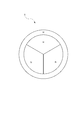
- the wavelength conversion member 5 does not have to have the phosphors 51 that emit light of different colors uniformly dispersed, and has fluorescent regions that emit light of different colors in parallel. Also good. That is, for example, as shown in FIG. 4, a red fluorescent region R containing a red phosphor, a green fluorescent region G containing a green phosphor, and a blue fluorescent region B containing a blue phosphor are arranged in the horizontal direction.
- the blue light emitted from the blue phosphor and the green light emitted from the green phosphor are not absorbed by the other phosphors 51, so that the energy conversion efficiency can be increased, and the wavelength In the conversion member 5, when the red fluorescent region R, the green fluorescent region G, and the blue fluorescent region B are laminated in the thickness direction in this order from the lower surface, the red phosphor closer to the LED element 3 deteriorates faster, The light emission color of the light emitting device 1 is likely to change. However, when the fluorescent regions are arranged in parallel in the horizontal direction, the light emission color of the light emitting device 1 changes because it is difficult to make a difference in the deterioration rate of the phosphors 51. Hateful.
- particles such as alumina, aluminum nitride, silicon carbide, aluminum, copper, silver, gold, carbon, sapphire, diamond and the like having high thermal conductivity are dispersed on the periphery of the wavelength conversion member 5.
- the formed heat dissipation area H may be formed. Thus, if the heat dissipation area H is formed at the periphery of the wavelength conversion member 5, the heat of the wavelength conversion member 5 can be released more efficiently.
- the UV cut is applied on the wavelength conversion member 5 or the translucent heat radiating member 6.
- a filter or the like may be provided.
- the inner wall surface of the recess 22 may function as a reflector by providing a metal film having a high reflectivity on the inner wall surface of the recess 22 of the base 2.
- the translucent heat radiating member 6 may function as a convex lens as shown in FIG.
- the LED element 3 may be connected to a wiring conductor provided on the base 2 using wire bonding.
- the translucent heat radiating member 6 and the wavelength converting member 5 may have the vertical positions opposite to those of the above-described embodiment. It may be placed on.
- a step portion 23 is formed on the side wall of the concave portion 22 of the base 2 as shown in FIG.
- the edge of the light transmissive heat radiating member 6 may be placed on the upper end surface thereof, and the light transmissive heat radiating member 6 is formed on the upper end surface 21 of the base 2 as shown in FIG. May be placed.
- the translucent heat radiating member 6 is larger than the wavelength converting member 5 in the lateral direction, and further, the base 2 is set larger than the translucent heat radiating member 6. For this reason, the side peripheral surface of the light emitting device 1 has a stepped shape. By setting the size of each member in this manner, the heat generated from the wavelength conversion member 5 can be more efficiently conducted and released to the base body 2 through the translucent heat radiating member 6.
- the number of LED elements 3 mounted on the base 2 is one, but a plurality of LED elements 3 may be mounted on the base 2 as shown in FIGS.
- the base 2 includes a substrate 2 a and a frame body 2 b installed on the substrate 2 a, and the upper surface of the substrate 2 a constitutes the bottom surface 221 of the recess 22.
- the wavelength conversion member 5 is larger than the translucent member 4 in the lateral direction, and more transparent than the wavelength conversion member 5.
- the light radiating member 6 is set larger.
- the present invention is not limited to the above-described embodiments, and may be configured by appropriately combining some or all of the various configurations described above without departing from the spirit of the present invention.
Landscapes
- Led Device Packages (AREA)
Abstract
本発明は、蛍光体を含有する波長変換部材の熱を効率的に放出することができるLED発光装置を提供するものであり、上端面に開口する凹部を有した基体と、前記凹部の底面に実装されたLED素子と、前記LED素子を封止する透光性部材と、蛍光体を含有し、前記透光性部材の上に載置された波長変換部材と、前記波長変換部材の上に載置されて前記凹部の開口部を覆う透光性放熱部材と、を備えているようにした。
Description
本発明は、LED素子から発された光を、蛍光体層によって波長変換して射出するLED発光装置に関するものである。
従来、窒化ガリウム系化合物半導体を用いて青色光又は紫外光を放射するLED素子と種々の蛍光体とを組み合わせることにより、白色をはじめとするLED素子の発光色とは異なる色の光を発する発光装置が開発されている(特許文献1)。このような、LED素子を用いた発光装置は、小型、省電力、長寿命等の長所があり、表示用光源や照明用光源として広く用いられている。特に近時では高出力、高輝度のLED素子が開発されてきており、その用途は益々増大の一途にある。
ところで、LED素子が高出力化することによって、LED素子の発熱量が大きく増大し、その熱によってLED素子そのものが劣化するという問題が生じている。また、蛍光体も熱に脆弱であることから、LED素子からの伝熱によって蛍光体が熱劣化すると一般には言われている。
そこで、従来は、LED素子の下に放熱板を敷き、ここから熱を発散させるようにしている。
しかしながら、実際には、蛍光体が熱を発し自身の劣化を促進しているという事実を本発明者は鋭意検討により初めて発見した。LED素子を放熱基板上に搭載し、その上を透明樹脂層で覆い、更にその上を蛍光体層で覆い、印加電圧3.5V、電流300mAの条件で実験したところ、LED素子の上面発光層部分が85℃、透明樹脂層の上面で55℃と言うように温度が下がっているにも拘わらず、蛍光体層の上面温度は65℃となっており、従来、軽視されていた蛍光体での発熱が顕著であることが確認された。
本発明はかかる問題点に鑑みなされたものであって、従来、軽視されていた蛍光体での発熱という点に初めて着目してなされたものであって、蛍光体を含有する波長変換部材の熱を効率的に放出することができるLED発光装置を提供することをその主たる所期課題としたものである。
すなわち本発明に係る発光装置は、上端面に開口する凹部を有した基体と、前記凹部の底面に実装されたLED素子と、前記LED素子を封止する透光性部材と、蛍光体を含有し、前記透光性部材の上に載置された波長変換部材と、前記波長変換部材の上に載置されて前記凹部の開口部を覆う透光性放熱部材と、を備えていることを特徴とする。
このようなものであれば、前記透光性放熱部材が前記波長変換部材の上に載置されて互いに密接していることにより、効率的に前記波長変換部材の熱を放出することができるので、前記波長変換部材に含まれる蛍光体の発光効率や輝度の低下や、熱劣化を、効果的に防ぐことができる。
本発明に係る発光装置の発光色の経時的な変化を抑制するためには、前記波長変換部材は、異なる色の光を発する蛍光領域が並設されてなるものであることが好ましい。
本発明に係る発光装置が白色光を発するものである場合、その色調むらを抑制するためには、前記LED素子は、近紫外光を発するものであり、前記蛍光体は、赤色光を発する蛍光体(以下、赤色蛍光体という。)、緑色光を発する蛍光体(以下、緑色蛍光体という。)、及び、青色光を発する蛍光体(以下、青色蛍光体という。)であることが好ましい。
本発明に係る発光装置では、前記透光性放熱部材と前記波長変換部材とは上下方向の位置が逆であってもよく、このような態様の発光装置もまた、本発明の1つである。すなわち、このような態様の本発明に係る発光装置は、上端面に開口する凹部を有した基体と、前記凹部の底面に実装されたLED素子と、前記LED素子を封止する透光性部材と、前記透光性部材の上に載置された透光性放熱部材と、前記透光性放熱部材の上に載置されて前記凹部の開口部を覆う、蛍光体を含有する波長変換部材と、を備えていることを特徴とする。
このような構成の本発明によれば、熱による蛍光体の変化を良好に抑制することができる。
以下に本発明の一実施形態について図面を参照して説明する。
本実施形態に係る発光装置1は、図1に示すように、上端面21に開口する凹部22を有した基体2と、凹部22の底面221に実装されたLED素子3と、LED素子3を封止する透光性部材4と、透光性部材4の上に載置された波長変換部材5と、波長変換部材5の上に載置されて凹部22の開口部を覆う透光性放熱部材6と、を備えたものである。
各部を詳述する。
基体2は、上端面21に開口する凹部22を有するものであり、例えば、アルミナや窒化アルミニウム等の熱伝導率が高い絶縁材料を成型してなるものが挙げられる。
基体2は、上端面21に開口する凹部22を有するものであり、例えば、アルミナや窒化アルミニウム等の熱伝導率が高い絶縁材料を成型してなるものが挙げられる。
基体2は、その凹部22の底面221に後述するLED素子3を実装するものであるが、当該底面221には、LED素子3が電気的に接続されるための配線導体(図示しない。)が形成されている。この配線導体が基体2内部に形成された配線層(図示しない。)を介して発光装置1の外表面に導出されて外部電気回路基板に接続されることにより、LED素子3と外部電気回路基板とが電気的に接続される。
基体2の凹部22の側壁には段部23が形成されており、その上端面には後述する透光性放熱部材6の縁部が載置されるように構成されている。
LED素子3は、例えば、サファイア基板上に窒化ガリウム系化合物半導体がn型層、発光層及びp型層の順に積層されたものであり、このようなLED素子3は青色光や紫外光を発する。
LED素子3は、窒化ガリウム系化合物半導体を下(凹部22の底面221側)にして凹部22の底面221に半田バンプや金バンプ等を用いてフリップチップ実装されている。
透光性部材4は、凹部22に充実されてLED素子3を封止しており、例えば、透光性及び耐熱性に優れ、LED素子3との屈折率差が小さいシリコーン樹脂等からなるものである。
波長変換部材5は、内部に蛍光体51を含有しており、透光性部材4の上に載置されている。このような波長変換部材5としては、例えば、透光性及び耐熱性に優れ、透光性部材4との屈折率差が小さいシリコーン樹脂中に蛍光体51が分散しているものが挙げられるが、蛍光体51が分散された未硬化のシリコーン樹脂を凹部22に充填してなるものであってもよく、シート状に加工されたものを所定の寸法にカットして用いるものであってもよい。
波長変換部材5が含有する蛍光体51としては特に限定されず、例えば、赤色蛍光体、緑色蛍光体、青色蛍光体、黄色蛍光体等が挙げられる。
透光性放熱部材6は、波長変換部材5の熱を放出するためのものであり、波長変換部材5の上に載置されて凹部22の開口部を覆っている。このような透光性放熱部材6としては、例えば、水晶、サファイア、ダイアモンド、窒化アルミニウム等の熱伝導率が高く透光性に優れた材料からなるものが挙げられる。
透光性放熱部材6が水晶からなるものである場合、水晶はサファイア等とは異なり劈開性を有しないので、図2及び図3に示すように、切頭円錐状にカットすることが可能であり、このため、基体2の凹部22を切頭円錐状にすることができる。凹部22が切頭円錐状であると、光性放熱部材6や波長変換部材5と基体2とが接する面積を増大させることができるので、これらの熱をより効率的に基体2へ伝導し放出することができる。また、凹部22が切頭円錐状であると、透光性放熱部材6や波長変換部材5の寸法精度が低くても、凹部22の内側周面に密に接触させることができるので、高い加工精度を必要とせずに、透光性放熱部材6や波長変換部材5と基体2との密着性を向上することができる。従って、より効果的に放熱性を高めることが可能となる。
本実施形態に係る発光装置1のうち、LED素子3として近紫外光を発するものを用い、蛍光体51として、赤色蛍光体、緑色蛍光体及び青色蛍光体を用いたものでは、LED素子3が発した近紫外光によって励起された赤色蛍光体、緑色蛍光体及び青色蛍光体が発する赤色光、緑色光及び青色光が混ざり合って白色光が発せられる。そして、LED素子3が発する近紫外光は発光装置1の発光色である白色に実質的に影響しない。このため、例えば、LED素子3が青色光を発するものであって、当該青色光が波長変換部材5に含まれる蛍光体51から発した光と混ざり合うように構成してある場合は、発光装置1の発光面において光路長の差に由来する色調むらが生じやすいが、LED素子3が近紫外光を発するものであって、蛍光体51が、赤色蛍光体、緑色蛍光体及び青色蛍光体である発光装置1は、このような色調むらを生じにくい。
そして、このような、LED素子3として近紫外光を発するものを用い、蛍光体51として、赤色蛍光体、緑色蛍光体及び青色蛍光体を用いた発光装置1が発する混合光は、プランク軌跡上を移動するものであって、極めて太陽光に近い自然な白色となる。
このような実施形態に係る発光装置1であれば、透光性放熱部材6が波長変換部材5の上に載置されていることにより、効率的に波長変換部材5の熱を放出することができるので、波長変換部材5に含まれる蛍光体51の発光効率や輝度の低下や、熱劣化を、効果的に防ぐことができる。
なお、本発明は前記実施形態に限られるものではない。
例えば、波長変換部材5は、互いに異なる色の光を発する蛍光体51が均一に分散されているものでなくともよく、互いに異なる色の光を発する蛍光領域が並設されているものであってもよい。すなわち、例えば、図4に示すように、赤色蛍光体を含有する赤色蛍光領域R、緑色蛍光体を含有する緑色蛍光領域G、及び、青色蛍光体を含有する青色蛍光領域Bが横方向に並設されていれば、青色蛍光体が発した青色光や緑色蛍光体が発した緑色光が他の蛍光体51に吸収されることがないのでエネルギー変換効率を高くすることができ、また、波長変換部材5において、赤色蛍光領域R、緑色蛍光領域G及び青色蛍光領域Bが下面からこの順で厚さ方向に積層されている場合は、LED素子3に近い赤色蛍光体ほど速く劣化するので、発光装置1の発光色が変化しやすいが、各蛍光領域が横方向に並設されている場合は、各蛍光体51の劣化速度に差が付きにくいので、発光装置1の発光色が変化しにくい。
また、図4に示すように、波長変換部材5の周縁には、熱伝導率の高い、アルミナ、窒化アルミニウム、炭化ケイ素、アルミニウム、銅、銀、金、カーボン、サファイア、ダイアモンド等の粒子が分散されてなる放熱領域Hが形成されていてもよい。このように波長変換部材5の周縁に放熱領域Hが形成されていれば、より一層効率的に波長変換部材5の熱を放出することができる。
更に、LED素子3から発した紫外光のうち、蛍光体51に吸収されずに外部に射出される紫外光を遮断するために、波長変換部材5又は透光性放熱部材6の上にUVカットフィルター等が設けられていてもよい。
また、基体2の凹部22の内側壁面に高反射率の金属薄膜を設けることにより、凹部22の内側壁面がリフレクタとして機能するものであってもよい。
更に、透光性放熱部材6は、図5に示すように、凸レンズとして機能するものであってもよい。
また、LED素子3は基体2に設けられた配線導体にワイヤボンディングを用いて接続されていてもよい。
更に、透光性放熱部材6と波長変換部材5とは、図6に示すように、上下方向の位置が前記実施形態と逆であってもよく、波長変換部材5が透光性放熱部材6の上に載置されていてもよい。
このように波長変換部材5が透光性放熱部材6の上に載置されている実施形態としては、図7に示すように、基体2の凹部22の側壁に段部23が形成されていて、その上端面に透光性放熱部材6の縁部が載置されるように構成されていてもよく、また、図8に示すように、基体2の上端面21に透光性放熱部材6が載置されていてもよい。
なお、図8に示す態様においては、横方向において、波長変換部材5より透光性放熱部材6の方が大きく、更に、透光性放熱部材6より基体2の方が大きく設定されており、このため、発光装置1の側周面は階段状をなしている。各部材の大きさをこのように設定することにより、波長変換部材5から発した熱を、透光性放熱部材6を経て基体2へ、より効率的に伝導し放出することができる。
また、前記実施形態では基体2に実装されているLED素子3は1個であるが、図9及び図10に示すように、複数のLED素子3が基体2に実装されていてもよい。なお、図9及び図10に示す実施形態では、基体2は、基板2aとその上に設置される枠体2bとからなり、基板2aの上面が凹部22の底面221を構成している。また、図9及び図10に示す実施形態では、放熱効率及び波長変換効率の点から、横方向において、透光性部材4より波長変換部材5の方が大きく、更に、波長変換部材5より透光性放熱部材6の方が大きく設定されている。
その他、本発明は上記の各実施形態に限られず、本発明の趣旨を逸脱しない限り、前述した種々の構成の一部又は全部を適宜組み合わせて構成してもよい。
このように本発明によれば、熱による蛍光体の変化を抑制したLED発光装置を得ることができる。
1・・・発光装置
2・・・基体
3・・・LED素子
4・・・透光性部材
5・・・波長変換部材
6・・・透光性放熱部材
2・・・基体
3・・・LED素子
4・・・透光性部材
5・・・波長変換部材
6・・・透光性放熱部材
Claims (4)
- 上端面に開口する凹部を有した基体と、
前記凹部の底面に実装されたLED素子と、
前記LED素子を封止する透光性部材と、
蛍光体を含有し、前記透光性部材の上に載置された波長変換部材と、
前記波長変換部材の上に載置されて前記凹部の開口部を覆う透光性放熱部材と、を備えていることを特徴とする発光装置。 - 前記波長変換部材は、異なる色の光を発する蛍光領域が並設されてなるものである請求項1記載の発光装置。
- 前記LED素子は、近紫外光を発するものであり、
前記蛍光体は、赤色光を発する蛍光体、緑色光を発する蛍光体、及び、青色光を発する蛍光体である請求項1記載の発光装置。 - 上端面に開口する凹部を有した基体と、
前記凹部の底面に実装されたLED素子と、
前記LED素子を封止する透光性部材と、
前記透光性部材の上に載置された透光性放熱部材と、
前記透光性放熱部材の上に載置されて前記凹部の開口部を覆う、蛍光体を含有する波長変換部材と、を備えていることを特徴とする発光装置。
Priority Applications (1)
| Application Number | Priority Date | Filing Date | Title |
|---|---|---|---|
| JP2010537181A JPWO2010123052A1 (ja) | 2009-04-22 | 2010-04-22 | 発光装置 |
Applications Claiming Priority (2)
| Application Number | Priority Date | Filing Date | Title |
|---|---|---|---|
| JP2009-104289 | 2009-04-22 | ||
| JP2009104289 | 2009-04-22 |
Publications (1)
| Publication Number | Publication Date |
|---|---|
| WO2010123052A1 true WO2010123052A1 (ja) | 2010-10-28 |
Family
ID=43011168
Family Applications (1)
| Application Number | Title | Priority Date | Filing Date |
|---|---|---|---|
| PCT/JP2010/057120 Ceased WO2010123052A1 (ja) | 2009-04-22 | 2010-04-22 | 発光装置 |
Country Status (2)
| Country | Link |
|---|---|
| JP (1) | JPWO2010123052A1 (ja) |
| WO (1) | WO2010123052A1 (ja) |
Cited By (13)
| Publication number | Priority date | Publication date | Assignee | Title |
|---|---|---|---|---|
| JP2012109400A (ja) * | 2010-11-17 | 2012-06-07 | Sharp Corp | 発光素子、発光装置および発光素子の製造方法 |
| CN102544312A (zh) * | 2010-12-15 | 2012-07-04 | 日东电工株式会社 | 光学半导体器件 |
| JP2013207049A (ja) * | 2012-03-28 | 2013-10-07 | Nec Corp | 波長変換体を用いた発光装置 |
| EP2614528A4 (en) * | 2009-06-18 | 2013-12-11 | Bridgelux Inc | LED ARRANGEMENT PACKAGING WITH STRONG CONDUCTIVE THERMAL COVER PLATE |
| CN104040739A (zh) * | 2011-11-08 | 2014-09-10 | Lg伊诺特有限公司 | 发光装置 |
| JP2015144301A (ja) * | 2015-03-10 | 2015-08-06 | 日東電工株式会社 | 光半導体装置 |
| KR101668965B1 (ko) * | 2015-11-27 | 2016-10-24 | 주식회사 지엘비젼 | 발광 다이오드 패키지 및 조명장치 |
| JP2017034218A (ja) * | 2015-08-03 | 2017-02-09 | 株式会社東芝 | 半導体発光装置 |
| EP3144724A4 (en) * | 2014-05-13 | 2017-12-13 | Appotronics (China) Corporation | Wavelength conversion device, light source system and projection system |
| WO2018155167A1 (ja) * | 2017-02-23 | 2018-08-30 | 日本電気硝子株式会社 | 発光デバイス及びその製造方法 |
| WO2018163691A1 (ja) * | 2017-03-10 | 2018-09-13 | 日本電気硝子株式会社 | 波長変換部材及び発光デバイス |
| JP2018151610A (ja) * | 2017-03-10 | 2018-09-27 | 日本電気硝子株式会社 | 波長変換部材及び発光デバイス |
| JP2022103159A (ja) * | 2018-01-29 | 2022-07-07 | 京セラ株式会社 | 発光装置、照明装置および生物育成用の照明装置 |
Citations (5)
| Publication number | Priority date | Publication date | Assignee | Title |
|---|---|---|---|---|
| JP2005217094A (ja) * | 2004-01-29 | 2005-08-11 | Kyocera Corp | 発光素子収納用パッケージおよび発光装置 |
| JP2005311170A (ja) * | 2004-04-23 | 2005-11-04 | Stanley Electric Co Ltd | 半導体発光装置 |
| JP2008192909A (ja) * | 2007-02-06 | 2008-08-21 | Stanley Electric Co Ltd | 発光装置およびその製造方法 |
| JP2009010049A (ja) * | 2007-06-26 | 2009-01-15 | Panasonic Electric Works Co Ltd | 発光装置 |
| JP2009016689A (ja) * | 2007-07-06 | 2009-01-22 | Toshiba Lighting & Technology Corp | 照明装置 |
-
2010
- 2010-04-22 JP JP2010537181A patent/JPWO2010123052A1/ja not_active Withdrawn
- 2010-04-22 WO PCT/JP2010/057120 patent/WO2010123052A1/ja not_active Ceased
Patent Citations (5)
| Publication number | Priority date | Publication date | Assignee | Title |
|---|---|---|---|---|
| JP2005217094A (ja) * | 2004-01-29 | 2005-08-11 | Kyocera Corp | 発光素子収納用パッケージおよび発光装置 |
| JP2005311170A (ja) * | 2004-04-23 | 2005-11-04 | Stanley Electric Co Ltd | 半導体発光装置 |
| JP2008192909A (ja) * | 2007-02-06 | 2008-08-21 | Stanley Electric Co Ltd | 発光装置およびその製造方法 |
| JP2009010049A (ja) * | 2007-06-26 | 2009-01-15 | Panasonic Electric Works Co Ltd | 発光装置 |
| JP2009016689A (ja) * | 2007-07-06 | 2009-01-22 | Toshiba Lighting & Technology Corp | 照明装置 |
Cited By (16)
| Publication number | Priority date | Publication date | Assignee | Title |
|---|---|---|---|---|
| EP2614528A4 (en) * | 2009-06-18 | 2013-12-11 | Bridgelux Inc | LED ARRANGEMENT PACKAGING WITH STRONG CONDUCTIVE THERMAL COVER PLATE |
| JP2012109400A (ja) * | 2010-11-17 | 2012-06-07 | Sharp Corp | 発光素子、発光装置および発光素子の製造方法 |
| CN102544312A (zh) * | 2010-12-15 | 2012-07-04 | 日东电工株式会社 | 光学半导体器件 |
| JP2012129361A (ja) * | 2010-12-15 | 2012-07-05 | Nitto Denko Corp | 光半導体装置 |
| CN104040739B (zh) * | 2011-11-08 | 2018-01-30 | Lg伊诺特有限公司 | 发光装置 |
| CN104040739A (zh) * | 2011-11-08 | 2014-09-10 | Lg伊诺特有限公司 | 发光装置 |
| EP2777080B1 (en) * | 2011-11-08 | 2019-07-03 | LG Innotek Co., Ltd. | Light emitting device |
| JP2013207049A (ja) * | 2012-03-28 | 2013-10-07 | Nec Corp | 波長変換体を用いた発光装置 |
| EP3144724A4 (en) * | 2014-05-13 | 2017-12-13 | Appotronics (China) Corporation | Wavelength conversion device, light source system and projection system |
| JP2015144301A (ja) * | 2015-03-10 | 2015-08-06 | 日東電工株式会社 | 光半導体装置 |
| JP2017034218A (ja) * | 2015-08-03 | 2017-02-09 | 株式会社東芝 | 半導体発光装置 |
| KR101668965B1 (ko) * | 2015-11-27 | 2016-10-24 | 주식회사 지엘비젼 | 발광 다이오드 패키지 및 조명장치 |
| WO2018155167A1 (ja) * | 2017-02-23 | 2018-08-30 | 日本電気硝子株式会社 | 発光デバイス及びその製造方法 |
| WO2018163691A1 (ja) * | 2017-03-10 | 2018-09-13 | 日本電気硝子株式会社 | 波長変換部材及び発光デバイス |
| JP2018151610A (ja) * | 2017-03-10 | 2018-09-27 | 日本電気硝子株式会社 | 波長変換部材及び発光デバイス |
| JP2022103159A (ja) * | 2018-01-29 | 2022-07-07 | 京セラ株式会社 | 発光装置、照明装置および生物育成用の照明装置 |
Also Published As
| Publication number | Publication date |
|---|---|
| JPWO2010123052A1 (ja) | 2012-10-25 |
Similar Documents
| Publication | Publication Date | Title |
|---|---|---|
| WO2010123052A1 (ja) | 発光装置 | |
| US7842960B2 (en) | Light emitting packages and methods of making same | |
| JP4338768B1 (ja) | 発光装置 | |
| US9420642B2 (en) | Light emitting apparatus and lighting apparatus | |
| JP2015126209A (ja) | 発光装置 | |
| US9812495B2 (en) | Light emitting device and lighting apparatus | |
| JP2013074273A (ja) | Led発光装置 | |
| JP2013038215A (ja) | 波長変換部材 | |
| JP2006049814A (ja) | 発光装置および照明装置 | |
| KR20170043126A (ko) | 색좌표와 열전도성이 향상된 고출력 led 패키지 및 그 제조방법. | |
| KR20130104975A (ko) | 발광장치 | |
| US9093626B2 (en) | Luminescence device | |
| KR101346122B1 (ko) | Led가 포함된 조명 시스템 | |
| JP6566791B2 (ja) | 発光装置 | |
| JP5067631B2 (ja) | 照明装置 | |
| JP2009231148A (ja) | 照明装置 | |
| US9093281B2 (en) | Luminescence device | |
| JP2009076494A (ja) | 発光装置 | |
| WO2010123051A1 (ja) | 発光装置 | |
| JP2011091126A (ja) | 発光装置(cobモジュール) | |
| JP2017050342A (ja) | 発光装置 | |
| JP2008153466A (ja) | 発光装置 | |
| JP2012119544A (ja) | Led発光体 | |
| KR20110052262A (ko) | 백색 발광 장치 | |
| JP2008294378A (ja) | 発光装置 |
Legal Events
| Date | Code | Title | Description |
|---|---|---|---|
| WWE | Wipo information: entry into national phase |
Ref document number: 2010537181 Country of ref document: JP |
|
| 121 | Ep: the epo has been informed by wipo that ep was designated in this application |
Ref document number: 10767109 Country of ref document: EP Kind code of ref document: A1 |
|
| NENP | Non-entry into the national phase |
Ref country code: DE |
|
| 122 | Ep: pct application non-entry in european phase |
Ref document number: 10767109 Country of ref document: EP Kind code of ref document: A1 |