WO2010131451A1 - 電子デバイス用エピタキシャル基板およびその製造方法 - Google Patents
電子デバイス用エピタキシャル基板およびその製造方法 Download PDFInfo
- Publication number
- WO2010131451A1 WO2010131451A1 PCT/JP2010/003162 JP2010003162W WO2010131451A1 WO 2010131451 A1 WO2010131451 A1 WO 2010131451A1 JP 2010003162 W JP2010003162 W JP 2010003162W WO 2010131451 A1 WO2010131451 A1 WO 2010131451A1
- Authority
- WO
- WIPO (PCT)
- Prior art keywords
- layer
- buffer
- superlattice
- substrate
- laminate
- Prior art date
- Legal status (The legal status is an assumption and is not a legal conclusion. Google has not performed a legal analysis and makes no representation as to the accuracy of the status listed.)
- Ceased
Links
Images


Classifications
-
- H—ELECTRICITY
- H10—SEMICONDUCTOR DEVICES; ELECTRIC SOLID-STATE DEVICES NOT OTHERWISE PROVIDED FOR
- H10D—INORGANIC ELECTRIC SEMICONDUCTOR DEVICES
- H10D62/00—Semiconductor bodies, or regions thereof, of devices having potential barriers
- H10D62/80—Semiconductor bodies, or regions thereof, of devices having potential barriers characterised by the materials
- H10D62/85—Semiconductor bodies, or regions thereof, of devices having potential barriers characterised by the materials being Group III-V materials, e.g. GaAs
- H10D62/854—Semiconductor bodies, or regions thereof, of devices having potential barriers characterised by the materials being Group III-V materials, e.g. GaAs further characterised by the dopants
-
- H—ELECTRICITY
- H10—SEMICONDUCTOR DEVICES; ELECTRIC SOLID-STATE DEVICES NOT OTHERWISE PROVIDED FOR
- H10P—GENERIC PROCESSES OR APPARATUS FOR THE MANUFACTURE OR TREATMENT OF DEVICES COVERED BY CLASS H10
- H10P14/00—Formation of materials, e.g. in the shape of layers or pillars
- H10P14/20—Formation of materials, e.g. in the shape of layers or pillars of semiconductor materials
-
- H—ELECTRICITY
- H10—SEMICONDUCTOR DEVICES; ELECTRIC SOLID-STATE DEVICES NOT OTHERWISE PROVIDED FOR
- H10D—INORGANIC ELECTRIC SEMICONDUCTOR DEVICES
- H10D30/00—Field-effect transistors [FET]
- H10D30/40—FETs having zero-dimensional [0D], one-dimensional [1D] or two-dimensional [2D] charge carrier gas channels
- H10D30/47—FETs having zero-dimensional [0D], one-dimensional [1D] or two-dimensional [2D] charge carrier gas channels having two-dimensional [2D] charge carrier gas channels, e.g. nanoribbon FETs or high electron mobility transistors [HEMT]
- H10D30/471—High electron mobility transistors [HEMT] or high hole mobility transistors [HHMT]
- H10D30/475—High electron mobility transistors [HEMT] or high hole mobility transistors [HHMT] having wider bandgap layer formed on top of lower bandgap active layer, e.g. undoped barrier HEMTs such as i-AlGaN/GaN HEMTs
-
- H—ELECTRICITY
- H10—SEMICONDUCTOR DEVICES; ELECTRIC SOLID-STATE DEVICES NOT OTHERWISE PROVIDED FOR
- H10D—INORGANIC ELECTRIC SEMICONDUCTOR DEVICES
- H10D62/00—Semiconductor bodies, or regions thereof, of devices having potential barriers
- H10D62/10—Shapes, relative sizes or dispositions of the regions of the semiconductor bodies; Shapes of the semiconductor bodies
- H10D62/17—Semiconductor regions connected to electrodes not carrying current to be rectified, amplified or switched, e.g. channel regions
- H10D62/351—Substrate regions of field-effect devices
- H10D62/357—Substrate regions of field-effect devices of FETs
-
- H—ELECTRICITY
- H10—SEMICONDUCTOR DEVICES; ELECTRIC SOLID-STATE DEVICES NOT OTHERWISE PROVIDED FOR
- H10D—INORGANIC ELECTRIC SEMICONDUCTOR DEVICES
- H10D62/00—Semiconductor bodies, or regions thereof, of devices having potential barriers
- H10D62/80—Semiconductor bodies, or regions thereof, of devices having potential barriers characterised by the materials
- H10D62/81—Semiconductor bodies, or regions thereof, of devices having potential barriers characterised by the materials of structures exhibiting quantum-confinement effects, e.g. single quantum wells; of structures having periodic or quasi-periodic potential variation
- H10D62/815—Semiconductor bodies, or regions thereof, of devices having potential barriers characterised by the materials of structures exhibiting quantum-confinement effects, e.g. single quantum wells; of structures having periodic or quasi-periodic potential variation of structures having periodic or quasi-periodic potential variation, e.g. superlattices or multiple quantum wells [MQW]
- H10D62/8161—Semiconductor bodies, or regions thereof, of devices having potential barriers characterised by the materials of structures exhibiting quantum-confinement effects, e.g. single quantum wells; of structures having periodic or quasi-periodic potential variation of structures having periodic or quasi-periodic potential variation, e.g. superlattices or multiple quantum wells [MQW] potential variation due to variations in composition or crystallinity, e.g. heterojunction superlattices
- H10D62/8162—Semiconductor bodies, or regions thereof, of devices having potential barriers characterised by the materials of structures exhibiting quantum-confinement effects, e.g. single quantum wells; of structures having periodic or quasi-periodic potential variation of structures having periodic or quasi-periodic potential variation, e.g. superlattices or multiple quantum wells [MQW] potential variation due to variations in composition or crystallinity, e.g. heterojunction superlattices having quantum effects only in the vertical direction, i.e. layered structures having quantum effects solely resulting from vertical potential variation
- H10D62/8164—Semiconductor bodies, or regions thereof, of devices having potential barriers characterised by the materials of structures exhibiting quantum-confinement effects, e.g. single quantum wells; of structures having periodic or quasi-periodic potential variation of structures having periodic or quasi-periodic potential variation, e.g. superlattices or multiple quantum wells [MQW] potential variation due to variations in composition or crystallinity, e.g. heterojunction superlattices having quantum effects only in the vertical direction, i.e. layered structures having quantum effects solely resulting from vertical potential variation comprising only semiconductor materials
-
- H—ELECTRICITY
- H10—SEMICONDUCTOR DEVICES; ELECTRIC SOLID-STATE DEVICES NOT OTHERWISE PROVIDED FOR
- H10P—GENERIC PROCESSES OR APPARATUS FOR THE MANUFACTURE OR TREATMENT OF DEVICES COVERED BY CLASS H10
- H10P10/00—Bonding of wafers, substrates or parts of devices
-
- H—ELECTRICITY
- H10—SEMICONDUCTOR DEVICES; ELECTRIC SOLID-STATE DEVICES NOT OTHERWISE PROVIDED FOR
- H10D—INORGANIC ELECTRIC SEMICONDUCTOR DEVICES
- H10D62/00—Semiconductor bodies, or regions thereof, of devices having potential barriers
- H10D62/80—Semiconductor bodies, or regions thereof, of devices having potential barriers characterised by the materials
- H10D62/85—Semiconductor bodies, or regions thereof, of devices having potential barriers characterised by the materials being Group III-V materials, e.g. GaAs
- H10D62/8503—Nitride Group III-V materials, e.g. AlN or GaN
-
- H—ELECTRICITY
- H10—SEMICONDUCTOR DEVICES; ELECTRIC SOLID-STATE DEVICES NOT OTHERWISE PROVIDED FOR
- H10P—GENERIC PROCESSES OR APPARATUS FOR THE MANUFACTURE OR TREATMENT OF DEVICES COVERED BY CLASS H10
- H10P14/00—Formation of materials, e.g. in the shape of layers or pillars
- H10P14/20—Formation of materials, e.g. in the shape of layers or pillars of semiconductor materials
- H10P14/29—Formation of materials, e.g. in the shape of layers or pillars of semiconductor materials characterised by the substrates
- H10P14/2901—Materials
- H10P14/2902—Materials being Group IVA materials
- H10P14/2904—Silicon carbide
-
- H—ELECTRICITY
- H10—SEMICONDUCTOR DEVICES; ELECTRIC SOLID-STATE DEVICES NOT OTHERWISE PROVIDED FOR
- H10P—GENERIC PROCESSES OR APPARATUS FOR THE MANUFACTURE OR TREATMENT OF DEVICES COVERED BY CLASS H10
- H10P14/00—Formation of materials, e.g. in the shape of layers or pillars
- H10P14/20—Formation of materials, e.g. in the shape of layers or pillars of semiconductor materials
- H10P14/32—Formation of materials, e.g. in the shape of layers or pillars of semiconductor materials characterised by intermediate layers between substrates and deposited layers
- H10P14/3202—Materials thereof
- H10P14/3214—Materials thereof being Group IIIA-VA semiconductors
- H10P14/3216—Nitrides
-
- H—ELECTRICITY
- H10—SEMICONDUCTOR DEVICES; ELECTRIC SOLID-STATE DEVICES NOT OTHERWISE PROVIDED FOR
- H10P—GENERIC PROCESSES OR APPARATUS FOR THE MANUFACTURE OR TREATMENT OF DEVICES COVERED BY CLASS H10
- H10P14/00—Formation of materials, e.g. in the shape of layers or pillars
- H10P14/20—Formation of materials, e.g. in the shape of layers or pillars of semiconductor materials
- H10P14/32—Formation of materials, e.g. in the shape of layers or pillars of semiconductor materials characterised by intermediate layers between substrates and deposited layers
- H10P14/3202—Materials thereof
- H10P14/3238—Materials thereof being insulating materials
-
- H—ELECTRICITY
- H10—SEMICONDUCTOR DEVICES; ELECTRIC SOLID-STATE DEVICES NOT OTHERWISE PROVIDED FOR
- H10P—GENERIC PROCESSES OR APPARATUS FOR THE MANUFACTURE OR TREATMENT OF DEVICES COVERED BY CLASS H10
- H10P14/00—Formation of materials, e.g. in the shape of layers or pillars
- H10P14/20—Formation of materials, e.g. in the shape of layers or pillars of semiconductor materials
- H10P14/32—Formation of materials, e.g. in the shape of layers or pillars of semiconductor materials characterised by intermediate layers between substrates and deposited layers
- H10P14/3242—Structure
- H10P14/3244—Layer structure
- H10P14/3251—Layer structure consisting of three or more layers
- H10P14/3252—Alternating layers, e.g. superlattice
-
- H—ELECTRICITY
- H10—SEMICONDUCTOR DEVICES; ELECTRIC SOLID-STATE DEVICES NOT OTHERWISE PROVIDED FOR
- H10P—GENERIC PROCESSES OR APPARATUS FOR THE MANUFACTURE OR TREATMENT OF DEVICES COVERED BY CLASS H10
- H10P14/00—Formation of materials, e.g. in the shape of layers or pillars
- H10P14/20—Formation of materials, e.g. in the shape of layers or pillars of semiconductor materials
- H10P14/34—Deposited materials, e.g. layers
- H10P14/3402—Deposited materials, e.g. layers characterised by the chemical composition
- H10P14/3414—Deposited materials, e.g. layers characterised by the chemical composition being group IIIA-VIA materials
- H10P14/3416—Nitrides
Definitions
- the present invention relates to an epitaxial substrate for electronic devices and a method for manufacturing the same, and more particularly to an epitaxial substrate for HEMT and a method for manufacturing the same.
- HEMT high electron mobility transistor
- FET field effect transistor
- a field effect transistor for example, as schematically shown in FIG. 1, a channel layer 22 and an electron supply layer 23 are stacked on a substrate 21, and a source electrode 24, It is formed by disposing the drain electrode 25 and the gate electrode 26, and when the device operates, electrons move in the order of the source electrode 24, the electron supply layer 23, the channel layer 22, the electron supply layer 23, and the drain electrode 25,
- the lateral direction is the current conduction direction, and the movement of electrons in the lateral direction is controlled by the voltage applied to the gate electrode 26.
- HEMT electrons generated at the junction interface between the electron supply layer 23 and the channel layer 22 having different band gaps can move at a higher speed than in a normal semiconductor.
- the movement of electrons in the lateral direction that is, the current is controlled by the gate voltage, but generally, the current does not become zero even when the gate voltage is turned off.
- the current that flows when the gate voltage is OFF is referred to as a leakage current.
- This leakage current is generally divided into a lateral leakage current and a longitudinal leakage current.
- the lateral leakage current is between two electrodes (for example, a source electrode 24 and a drain electrode 25 arranged on the surface of the electron supply layer 23).
- the vertical leakage current refers to the leakage current flowing between the two electrodes disposed on the surface on the electron supply layer 23 side and on the surface on the substrate 21 side, respectively.
- Patent Document 1 discloses a HEMT structure including a superlattice buffer layer, a channel layer, and an electron supply layer on a conductive SiC substrate.
- Patent Document 2 discloses a HEMT structure including a superlattice buffer layer to which a p-type impurity is added, a channel layer, and an electron supply layer via a GaN intervening layer on a Si or SiC substrate.
- An object of the present invention is to use a conductive SiC substrate as a substrate, to achieve both a reduction in lateral leakage current and a lateral withstand voltage characteristic, to improve the longitudinal withstand voltage and to suppress the occurrence of cracks. Another object is to provide an epitaxial substrate for an electronic device and a method for manufacturing the same.
- the first layer is made of an AlN material
- the epitaxial substrate for electronic devices as described in said (1) or (2).
- the epitaxial substrate for electronic devices according to the above (1), (2) or (3) made of a material.
- a first layer made of a material and B a3 Al b3 Ga having a different band gap from the first layer c3 In d3 N (0 ⁇ a 3 ⁇ 1, 0 ⁇ b 3 ⁇ 1, 0 ⁇ c 3 ⁇ 1, 0 ⁇ d 3 1, a 3 + b 3
- the superlattice laminate and the buffer side portion of the main laminate both have a C concentration of 1 ⁇ 10 18 / cm 3 or more, and the epitaxial substrate for electronic devices according to (6) above Production method.
- An epitaxial substrate for an electronic device comprises an initial growth layer made of an Al-containing group III nitride, a buffer having a predetermined superlattice laminate, and a predetermined main laminate on a conductive SiC substrate,
- the buffer side portion of the body and / or the main laminate has a C concentration of 1 ⁇ 10 18 / cm 3 or more, so that not only the reduction of the lateral leakage current and the lateral withstand voltage characteristics can be achieved well, The vertical breakdown voltage can be improved.
- a conductive SiC substrate it is possible to improve heat dissipation and further reduce the occurrence of cracks.
- the present invention also includes an initial growth layer made of an Al-containing group III nitride and a buffer having a predetermined superlattice laminate, and a predetermined main laminate, on the buffer side of the superlattice laminate and / or the main laminate. Since the portion has a C concentration of 1 ⁇ 10 18 / cm 3 or more, not only can the lateral leakage current be reduced and the lateral breakdown voltage characteristics can be improved, but also the vertical breakdown voltage can be improved. By using a conductive SiC substrate, it is possible to produce an epitaxial substrate for electronic devices with improved heat dissipation and reduced occurrence of cracks.
- FIG. 2 schematically shows a cross-sectional structure of an epitaxial substrate for an electronic device according to the present invention. Note that FIG. 2 shows the thickness direction exaggerated for convenience of explanation.
- an electronic device epitaxial substrate 1 is an electronic device epitaxial substrate having a horizontal direction as a current conduction direction, and includes a conductive SiC single crystal substrate 2 and a conductive SiC single crystal substrate.
- a buffer 3 as an insulating layer formed on 2 and a main laminate 4 formed by epitaxially growing a plurality of group III nitride layers on the buffer 3. The buffer 3 is in contact with the Si single crystal substrate 2.
- the first layer 6a and the first layer 6a B a3 Al b3 Ga c3 In d3 N (0 ⁇ a 3 ⁇ 1, 0 ⁇ b 3 ⁇ 1, 0
- the conductive SiC substrate can improve heat dissipation and further suppress the occurrence of cracks.
- the conductive SiC single crystal substrate 2 those having various crystal structures can be used, but those having 4H or 6H are preferable.
- the plane orientation is not particularly specified, and the (0001), (10-10), (11-20) plane, etc. can be used, but the (0001) plane of group III nitride is grown with good surface flatness. For this, it is desirable to use the (0001) plane. Moreover, it may be p-type or n-type conductivity type.
- the conductivity of the SiC single crystal substrate 2 a substrate having a low resistance of 1000 ⁇ ⁇ cm or less can be appropriately used according to the application. In the present application, a SiC substrate having a resistivity of 1000 ⁇ ⁇ cm or less is referred to as a conductive SiC substrate.
- the conductive SiC single crystal substrate 2 As a method for producing the conductive SiC single crystal substrate 2, various methods such as a sublimation method can be used, and SiC can be homoepitaxially grown on the substrate surface. It is also possible to use a substrate in which a thin film made of an oxide film, nitride film, or carbonized film is formed. The reason why it is difficult to increase the resistance in the SiC substrate is that nitrogen, which is the main component in the atmosphere, is likely to be mixed as an impurity, and if mixed, it becomes an n-type dopant and lowers the resistivity.
- the material is more preferable, and AlN is most preferable. This is because the tensile stress in the superlattice laminate can be effectively suppressed by making the composition relationship as described above.
- the AlN material here may contain trace impurities of 1% or less regardless of intended or unintentional, for example, Ga, In, Si, H, O, C, Impurities such as B, Mg, As, and P can be included.
- the initial growth layer preferably has a thickness in the range of 10 nm to 200 nm. If the initial layer is too thin, the tensile stress in the superlattice laminate cannot be sufficiently suppressed, so cracks may occur in the superlattice laminate, and if it is too thick, the tensile stress in the initial layer is accumulated. Therefore, cracks in the initial layer may occur.
- the lateral direction is the current conduction direction
- a current flows from the source electrode 24 to the drain electrode 25 mainly in the width direction of the stacked body as shown in FIG. This means that the current flows mainly in the longitudinal direction, that is, in the thickness direction of the stacked body, as in a structure in which a semiconductor is sandwiched between a pair of electrodes.
- alternately laminating superlattice laminates means laminating so as to periodically include the first layer 6a and the second layer 6b. It is possible to include a layer (for example, a composition transition layer) other than the first layer 6a and the second layer 6b.
- the C concentration of the portion 4 ′ on the buffer 3 side of the main laminate 4 is preferably higher than the C concentration of the superlattice laminate 6.
- the portion 4 ′ a phenomenon in which dislocations bend horizontally or obliquely due to the difference in the lattice constant between the buffer 3 and the main laminate 4 is observed, and a path through which a leak current easily flows is formed. Therefore, the portion 4 'is more likely to have a leakage current than the buffer layer 3, and in order to suppress this leakage current, the C concentration as described above is desirable.
- the thickness of the portion 4 ′ on the buffer 3 side of the main laminate 4 is less than 0.1 ⁇ m, there is a possibility that dislocation bends may be prominent even in a portion with a low C concentration. It is preferable to set to.
- the upper limit of the thickness of the portion 4 ′ is not particularly specified from the viewpoint of improving the breakdown voltage and reducing the leakage current, and is appropriately set from the viewpoint of suppressing warpage and cracking of the substrate.
- the first layer 6a constituting the superlattice laminate 6 is made of AlN material
- it consists of. Since the band gap difference between the first layer 6a and the second layer 6b improves the longitudinal breakdown voltage, it is preferable to make the composition difference as large as possible and the band gap difference as large as possible.
- the largest band gap difference is AlN (6.2 eV) and GaN (3.5 eV). Therefore, it is preferable to form a superlattice structure using an AlGaN material.
- the compositional difference is preferably 0.5 or more.
- the upper limit of the composition difference it is desirable that the composition difference is large.
- the second layer having a small band gap should contain at least Al, and the composition of Al The difference is preferably less than 1. This is because when at least Al is contained, C can be taken in more efficiently.
- the number of superlattice pairs is at least 40 pairs and the total thick film is 1 ⁇ m or more, because variations in breakdown voltage can be reduced. The thicker the superlattice layer is, the higher the withstand voltage can be. Therefore, it is preferable for the use at a high voltage, but there is a disadvantage that the raw material cost increases. select.
- the thickness of the first layer 6a having a large band gap should be not less than a thickness at which tunnel current can be suppressed and not more than a thickness at which cracks do not occur.
- the thickness of the second layer 6b is appropriately set from the viewpoint of crack suppression and warpage control, but in order to effectively exhibit the strain buffering effect of the superlattice laminate structure and suppress the occurrence of cracks,
- the thickness of the small layer is preferably thicker than that of the layer having a large band gap and is 40 nm or less. Further, it is not always necessary to laminate the superlattice laminate with the same film thickness and the same composition.
- the epitaxial substrate 1 for electronic devices can be used for various applications in which the horizontal direction is the current conduction direction. It is preferably used for HEMT.
- the electron supply layer 4b made of a material can be provided.
- both layers can be composed of a single composition or a plurality of compositions.
- at least a portion of the channel layer 4a in contact with the electron supply layer 4b is made of a GaN material.
- the portion of the channel layer 4a opposite to the buffer layer preferably has a low C concentration, and is preferably set to 4 ⁇ 10 16 / cm 3 or less. This is because this portion corresponds to a current conducting portion of the electronic device, and therefore it is desirable that the portion not contain impurities that impede conductivity or generate current collapse. Further, in order to suppress leakage due to residual carriers due to n-type impurities, it is desirable to exist at 1 ⁇ 10 15 / cm 3 or more.
- a buffer 3 as an insulating layer is formed on a conductive SiC single crystal substrate 2, and a main laminate 4 having a HEMT structure in which a plurality of group III nitride layers are epitaxially grown on the buffer 3.
- the amount of other impurities is not particularly specified, but it is preferable to suppress the incorporation of donor impurities (Si, O, Ge) having relatively shallow impurity levels, but to the extent that such donor levels can be compensated. If C is contained, a certain amount of contamination is allowed.
- the impurity concentration measured the impurity concentration distribution of the depth direction, etching from the surface side using SIMS analysis. At this time, when the composition of the group III element is changed only in the portion 4 ′, or the C concentration or the composition of the group III element in the portion on the opposite side of the buffer layer of the channel layer 4a from the portion 4 ′ is changed sharply. It can be changed or can be changed continuously.
- C added to the superlattice laminate 6 and the portion 4 'on the buffer 3 side of the main laminate 4 can be added by the following several methods when grown using the CVD method.
- First method A source gas containing C is added separately during group III nitride growth. Examples include methane, ethane, ethylene, acetylene, benzene, cyclopentane and the like.
- Second method A methyl group, an ethyl group, or the like in the organic metal is mixed in the epitaxial growth layer according to the growth group III nitride growth conditions. The concentration of C added to the epitaxial growth layer can be adjusted by appropriately setting the growth temperature, growth pressure, growth rate, ammonia flow rate, hydrogen flow rate, nitrogen flow rate, etc.
- the C concentration of the superlattice laminate 6 is a measured value obtained by removing a half of the thickness of the superlattice laminate 6 by SIMS.
- the C concentration of the portion 4 ′ on the buffer 3 side of the main laminate 4 is a measured value obtained by removing a half of the thickness of the portion 4 ′ by SIMS.
- 1 and 2 show examples of typical embodiments, and the present invention is not limited to these embodiments.
- an intermediate layer that does not adversely affect the effects of the present invention can be inserted between the layers, another superlattice layer can be inserted, or the composition can be graded.
- a nitride film, a carbide film, an Al layer, or the like can be formed on the surface of the conductive SiC single crystal.
- the laminated structure of the present invention is not limited to a conductive SiC substrate, but various metal materials and low-resistance semiconductor materials (Ge, GaN, AlGaN, GaAs, ZnO, etc.) that generate cracks when the initial growth layer is made of GaN. Extension to other conductive substrates made of is possible. Thereby, even when a conductive substrate is used, it is possible to obtain the effects of the present application that suppress the generation of cracks, reduce the lateral leakage current, and improve the lateral and longitudinal breakdown voltage characteristics.
- various metal materials and low-resistance semiconductor materials Ga, GaN, AlGaN, GaAs, ZnO, etc.
- An initial growth layer (AlN material: thickness 100 nm) on a 300 ⁇ m thick (0001) 3 inch 6H-SiC single crystal substrate with specific resistance of 1 ⁇ 10 -1 ⁇ ⁇ cm, 10 ⁇ ⁇ cm, 100 ⁇ ⁇ cm, respectively
- a superlattice stack (AlN: 4 nm thick and Al 0.15 Ga 0.85 N: 25 nm thick, total 85 layers) is formed to form a buffer, and a channel layer (GaN material: thickness is formed on this superlattice stack.
- TMA trimethylaluminum
- TMG trimethylgallium
- ammonia was used as a group V material
- hydrogen and nitrogen gas were used as carrier gases.
- the film-forming temperature here means the temperature of the substrate itself measured using a radiation thermometer during growth.
- the C concentration SIMS measurement was performed by etching from the epitaxial layer side, using a Cameca measuring device, using Cs ⁇ as the ion source, and ion energy of 8 keV.
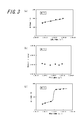
- FIG. 3A, 3B, and 3C show the measurement results of the lateral breakdown voltage, the lateral leakage current, and the vertical breakdown voltage of Sample 2.
- FIG. The measurement was performed as follows. Longitudinal direction: An ohmic electrode with a Ti / Al laminated structure of 80 ⁇ m ⁇ is formed on the substrate surface, the outside of the ohmic electrode is etched to a thickness of 50 nm, the back surface of the substrate is grounded to a metal plate, and the current value flowing between both electrodes is measured Measured against voltage.
- Ti / Al laminated structure ohmic electrodes consisting of 200 ⁇ m square (squares) are formed with each side spaced apart by 10 ⁇ m and etched around the ohmic electrode with a thickness of 150nm, then both electrodes The current value flowing between them was measured with respect to the voltage.
- the two electrodes are insulated with insulating oil.
- an insulating plate is disposed under the substrate.
- the vertical breakdown voltage is a voltage value in which the vertical current value converted to a value per unit area in the above electrode area reaches 10 -4 A / cm 2
- the horizontal breakdown voltage is the horizontal current.
- a value obtained by converting the value into a value per length of one side of the electrode reaches a voltage of 10 ⁇ 4 A / cm, and a lateral leakage current is defined as a current value at 100 V in the lateral direction.
- the C concentration of the superlattice laminate 6 was obtained by measuring a location where 1/2 of the thickness of the superlattice laminate 6 was removed by SIMS.
- the C concentration in the portion 4 ′ on the buffer 3 side of the main laminate 4 was obtained by measuring the location where 1/2 of the thickness of the portion 4 ′ was removed by SIMS.
- the sheet resistance value was 440 ⁇ / ⁇ or less (square), and the mobility was 1570 cm 2 / Vs or more. It has been confirmed that it exhibits good characteristics.
- the surface of the epitaxial substrate produced in all the experimental examples was observed with an optical microscope (100 times), but no cracks were observed.
- Example 2 Sample of Experimental Example 1 except that the growth pressure of the superlattice laminate was set to 10 kPa, the C concentration in the buffer side portion of the main laminate was changed, and the growth temperature and pressure of each layer were performed under the conditions shown in Table 2. Samples 4 to 6 were prepared in the same manner as in 1-3. Adjust the C concentration by adjusting the table in P 2, and increasing the C concentration by reducing the deposition pressure. The C concentration of the superlattice laminate was in the range of 1.5 to 2.5 ⁇ 10 18 / cm 3 in all results.
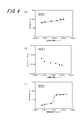
- FIGS. 4A, 4B, and 4C show the measurement results of the lateral breakdown voltage, the lateral leakage current, and the vertical breakdown voltage of the sample 4.
- FIG. 4 As a result of changing the C concentration of the main laminate, the lateral breakdown voltage and the lateral leakage current are hardly changed, whereas the vertical breakdown voltage of the sample 4 is the C concentration in the buffer side portion of the main laminate. When the value exceeds 1 ⁇ 10 18 / cm 3 , it can be confirmed that the value increases specifically and rapidly.
- the samples 5 and 6 having different specific resistances of the Si single crystal substrates used were not significantly different from the results shown in FIGS. 4 (a) to 4 (c). .
- the surface of the epitaxial substrate produced in all the experimental examples was observed with an optical microscope (100 times), but no cracks were observed.
- the longitudinal breakdown voltage It can be seen that can be effectively increased.
- Example 3 The same method as Sample 2 of Experimental Example 1 except that the initial growth layer was formed of GaN material (thickness: 20 nm) grown at 700 ° C., and the growth temperature and pressure of each layer were performed under the conditions shown in Table 3. Sample 7 was prepared by the above.
- Example 4 Samples 8 to 10 were prepared by the same method as Samples 1 to 3 in Experimental Example 1 except that the initial growth layer was made of Al 0.5 Ga 0.5 N material, and the same experiment was performed. As a result, the same results as in Fig. 3 (a), Fig. 3 (b) and Fig. 3 (c) were confirmed in all samples, sheet resistance value 450 ⁇ / ⁇ or less (square), and mobility 1550cm 2 / Vs. It has been confirmed that the above characteristics are good. The surface of the epitaxial substrate produced in all the experimental examples was observed with an optical microscope (100 times), but no cracks were observed.
- Example 5 Samples 11 to 13 were prepared by the same method as Samples 4 to 6 in Experimental Example 2, except that the initial growth layer was made of Al 0.5 Ga 0.5 N material, and the same experiment was performed. As a result, the same results as in FIGS. 4 (a), 4 (b) and 4 (c) were confirmed for all the samples. The surface of the epitaxial substrate produced in all the experimental examples was observed with an optical microscope (100 times), but no cracks were observed.
- the epitaxial substrate for electronic devices of the present invention comprises a buffer having an Al-containing initial growth layer and a predetermined superlattice laminate on a conductive SiC substrate, and a predetermined main laminate, the superlattice laminate and / or the main laminate.
- the buffer side portion of the laminate has a C concentration of 1 ⁇ 10 18 / cm 3 or higher, which not only achieves good reduction in lateral leakage current and lateral breakdown characteristics, but also improves vertical breakdown voltage. Can be made.
- a conductive SiC substrate it is possible to improve heat dissipation and further reduce the occurrence of cracks.
Landscapes
- Junction Field-Effect Transistors (AREA)
- Crystals, And After-Treatments Of Crystals (AREA)
- Chemical Vapour Deposition (AREA)
Abstract
Description
(1)導電性SiC単結晶基板と、該SiC単結晶基板上に形成した絶縁層としてのバッファと、該バッファ上に複数層のIII族窒化物層をエピタキシャル成長させて形成した主積層体とを具え、横方向を電流導通方向とする電子デバイス用エピタキシャル基板であって、前記バッファは、前記SiC単結晶基板と接する初期成長層および該初期成長層上の超格子多層構造からなる超格子積層体を少なくとも有し、前記初期成長層はBa1Alb1Gac1Ind1N(0≦a1≦1, 0<b1≦1, 0≦c1≦1, 0≦d1≦1, a1+b1+c1+d1=1)材料からなり、かつ前記超格子積層体はBa2Alb2Gac2Ind2N(0≦a2≦1, 0≦b2≦1, 0≦c2≦1, 0≦d2≦1, a2+b2+c2+d2=1)材料からなる第1層および該第1層とはバンドギャップの異なるBa3Alb3Gac3Ind3N(0≦a3≦1, 0≦b3≦1, 0≦c3≦1, 0≦d3≦1, a3+b3+c3+d3=1)材料からなる第2層を交互に積層してなり、前記超格子積層体、または、前記主積層体の前記バッファ側の部分の少なくとも一方は、C濃度が1×10¹⁸/cm3以上であることを特徴とする電子デバイス用エピタキシャル基板。
第1の方法:Cを含む原料ガスを、III族窒化物成長中に別途添加する。メタン・エタン・エチレン・アセチレン・ベンゼン・シクロペンタン等が例示される。
第2の方法:有機金属中のメチル基・エチル基等を、成長III族窒化物成長条件によりエピタキシャル成長層に混入させる。有機金属の分解を抑えるように、成長温度・成長圧力・成長速度・成長時のアンモニア流量・水素流量・窒素流量等を適宜設定することにより、エピタキシャル成長層に添加されるC濃度を調整することが可能である。
なお、本願では、超格子積層体6のC濃度は、SIMSにより、超格子積層体6の厚さの1/2を除去した箇所の測定値とする。主積層体4のバッファ3側の部分4´のC濃度は、SIMSにより、前記部分4´の厚さの1/2を除去した箇所の測定値とする。
比抵抗がそれぞれ1×10-1Ω・cm、10Ω・cm、100Ω・cmの300μm厚の(0001)面3インチ6H-SiC単結晶基板上に、初期成長層(AlN材料:厚さ100nm)および超格子積層体(AlN:膜厚4nmとAl0.15Ga0.85N:膜厚25nm、合計85層)を成長させてバッファを形成し、この超格子積層体上にチャネル層(GaN材料:厚さ1.5μm)および電子供給層(Al0.25Ga0.75N材料:厚さ20nm)をエピタキシャル成長させてHEMT構造の主積層体を形成して試料1~3を得た。超格子積層体のC濃度を変化させ、主積層体のバッファ側の部分のC濃度は、いずれの結果も、1.5~2.0×10¹⁸/cm3の範囲であった。また、チャネル層の電子供給層側の部分は、C濃度が0.8~3.5×1016/cm3の範囲であった。各層の成長温度、圧力を表1に示す。表中P1を調整することによりC濃度を調整し、成膜圧力を下げることによりC濃度を増加させている。成長方法としてはMOCVD法を使用し、III族原料としては、TMA(トリメチルアルミニウム)・TMG(トリメチルガリウム)、V族原料としてはアンモニアを用い、キャリアガスとして、水素および窒素ガスを用いた。ここでいう成膜温度は、成長中に放射温度計を用いて測定した、基板自体の温度を意味する。なお、C濃度のSIMS測定は、エピタキシャル層側からエッチングを行い、Cameca製の測定装置で、イオン源としてCs-を用い、イオンエネルギーは8keVで行った。

縦方向:基板表面に80μmφからなるTi/Al積層構造のオーミック電極を形成し、オーミック電極外側を50nmの厚みでエッチングした後、基板裏面を金属板に接地し、両電極間に流れる電流値を電圧に対して測定した。
横方向:200μm□(四角)からなるTi/Al積層構造のオーミック電極を各々の一辺を10μmの距離を離して配置して形成し、前記オーミック電極周囲を150nmの厚みでエッチングした後、両電極間に流れる電流値を電圧に対して測定した。この際、空気中の放電を抑制するため、絶縁油で両電極間を絶縁している。また、基板裏面へのリークの影響をなくすため、基板下には絶縁板を配置している。
本実験例において、縦方向耐圧は縦方向の電流値を上記電極面積で単位面積当たりの値に換算した値が10-4A/cm2に達する電圧値で、横方向耐圧は横方向の電流値を上記電極の1辺の長さ当たりの値に換算した値が10-4A/cmに達する電圧値で、横方向リーク電流は横方向が100Vでの電流値で、それぞれ定義する。
超格子積層体6のC濃度は、SIMSにより、超格子積層体6の厚さの1/2を除去した箇所を測定することにより得た。主積層体4のバッファ3側の部分4´のC濃度は、SIMSにより、前記部分4´の厚さの1/2を除去した箇所を測定値することにより得た。
光学顕微鏡(100倍)で、全ての実験例で作製したエピタキシャル基板の表面を観察したが、クラックの発生は認められなかった。
超格子積層体の成長圧力を10kPaとして、主積層体のバッファ側の部分のC濃度を変化させ、各層の成長温度、圧力を表2に示す条件で行ったこと以外は、実験例1の試料1~3と同様の方法により試料4~6を作製した。表中P2を調整することによりC濃度を調整し、成膜圧力を下げることによりC濃度を増加させている。超格子積層体のC濃度は、いずれの結果も1.5~2.5×10¹⁸/cm3の範囲であった。

光学顕微鏡(100倍)で、全ての実験例で作製したエピタキシャル基板の表面を観察したが、クラックの発生は認められなかった。
初期成長層を700℃で成長したGaN材料(厚さ:20nm)で形成し、各層の成長温度、圧力を表3に示す条件で行ったこと以外は、実験例1の試料2と同様の方法により試料7を作製した。

初期成長層を、Al0.5Ga0.5N材料とした以外は、実験例1の試料1~3と同様の方法により、試料8~10を作成し、同様の実験を行った。その結果、図3(a)、図3(b)および図3(c)と同様の結果が全ての試料で確認され、シート抵抗値450Ω/□以下(四角)、移動度は1550cm2/Vs以上と良好な特性を示すことが確認されていた。
光学顕微鏡(100倍)で、全ての実験例で作製したエピタキシャル基板の表面を観察したが、クラックの発生は認められなかった。
初期成長層を、Al0.5Ga0.5N材料とした以外は、実験例2の試料4~6と同様の方法により、試料11~13を作成し、同様の実験を行った。その結果、図4(a)、図4(b)および図4(c)と同様の結果が全ての試料で確認された。
光学顕微鏡(100倍)で、全ての実験例で作製したエピタキシャル基板の表面を観察したが、クラックの発生は認められなかった。
2 導電性SiC単結晶基板
3 バッファ
4 主積層体
4a チャネル層
4b 電子供給層
5 初期成長層
6 超格子積層体
6a 第1層
6b 第2層
Claims (7)
- 導電性SiC単結晶基板と、該SiC単結晶基板上に形成した絶縁層としてのバッファと、該バッファ上に複数層のIII族窒化物層をエピタキシャル成長させて形成した主積層体とを具え、横方向を電流導通方向とする電子デバイス用エピタキシャル基板であって、前記バッファは、前記SiC単結晶基板と接する初期成長層および該初期成長層上の超格子多層構造からなる超格子積層体を少なくとも有し、前記初期成長層はBa1Alb1Gac1Ind1N(0≦a1≦1, 0<b1≦1, 0≦c1≦1, 0≦d1≦1, a1+b1+c1+d1=1)材料からなり、かつ前記超格子積層体はBa2Alb2Gac2Ind2N(0≦a2≦1, 0≦b2≦1, 0≦c2≦1, 0≦d2≦1, a2+b2+c2+d2=1)材料からなる第1層および該第1層とはバンドギャップの異なるBa3Alb3Gac3Ind3N(0≦a3≦1, 0≦b3≦1, 0≦c3≦1, 0≦d3≦1, a3+b3+c3+d3=1)材料からなる第2層を交互に積層してなり、前記超格子積層体、または、前記主積層体の前記バッファ側の部分の少なくとも一方は、C濃度が1×10¹⁸/cm3以上であることを特徴とする電子デバイス用エピタキシャル基板。
- 前記超格子積層体、および、前記主積層体の前記バッファ側の部分は、ともにC濃度が1×10¹⁸/cm3以上である請求項1に記載の電子デバイス用エピタキシャル基板。
- 前記第1層がAlN材料からなり、前記第2層がAlb3Gac3N(a3=0, 0<b3≦0.5, 0.5≦c3<1, d3=0)材料からなる請求項1または2に記載の電子デバイス用エピタキシャル基板。
- 前記初期成長層がBa1Alb1Gac1Ind1N(0≦a1≦1, 0.5≦b1≦1, 0≦c1≦1, 0≦d1≦1, a1+b1+c1+d1=1)材料からなる請求項1、2または3に記載の電子デバイス用エピタキシャル基板。
- 前記初期成長層がAlN材料からなる請求項1、2または3に記載の電子デバイス用エピタキシャル基板。
- 導電性SiC単結晶基板と、該SiC単結晶基板上に形成した絶縁層としてのバッファと、該バッファ上に複数層のIII族窒化物層をエピタキシャル成長させて形成した主積層体とを具え、横方向を電流導通方向とする電子デバイス用エピタキシャル基板の製造方法であって、前記バッファは、前記SiC単結晶基板と接する初期成長層および該初期成長層上の超格子多層構造からなる超格子積層体を少なくとも有し、前記初期成長層はBa1Alb1Gac1Ind1N(0≦a1≦1, 0<b1≦1, 0≦c1≦1, 0≦d1≦1, a1+b1+c1+d1=1)材料からなり、かつ前記超格子積層体はBa2Alb2Gac2Ind2N(0≦a2≦1, 0≦b2≦1, 0≦c2≦1, 0≦d2≦1, a2+b2+c2+d2=1)材料からなる第1層および該第1層とはバンドギャップの異なるBa3Alb3Gac3Ind3N(0≦a3≦1, 0≦b3≦1, 0≦c3≦1, 0≦d3≦1, a3+b3+c3+d3=1)材料からなる第2層を交互に積層してなり、前記超格子積層体、または、前記主積層体の前記バッファ側の部分の少なくとも一方は、C濃度が1×10¹⁸/cm3以上であることを特徴とする電子デバイス用エピタキシャル基板の製造方法。
- 前記超格子積層体、および、前記主積層体の前記バッファ側の部分は、ともにC濃度が1×10¹⁸/cm3以上である請求項6に記載の電子デバイス用エピタキシャル基板の製造方法。
Priority Applications (4)
| Application Number | Priority Date | Filing Date | Title |
|---|---|---|---|
| KR1020117029263A KR101321625B1 (ko) | 2009-05-11 | 2010-05-10 | 전자 디바이스용 에피택셜 기판 및 그 제조방법 |
| CN201080031291.0A CN102460664B (zh) | 2009-05-11 | 2010-05-10 | 电子器件用外延衬底及其制造方法 |
| EP10774710.7A EP2432005A4 (en) | 2009-05-11 | 2010-05-10 | EPITACTICAL SUBSTRATE FOR ELECTRONIC EQUIPMENT AND METHOD FOR THE PRODUCTION THEREOF |
| US13/319,910 US8426893B2 (en) | 2009-05-11 | 2010-05-10 | Epitaxial substrate for electronic device and method of producing the same |
Applications Claiming Priority (4)
| Application Number | Priority Date | Filing Date | Title |
|---|---|---|---|
| JP2009-114860 | 2009-05-11 | ||
| JP2009114860 | 2009-05-11 | ||
| JP2010107821A JP4685961B2 (ja) | 2009-05-11 | 2010-05-10 | 電子デバイス用エピタキシャル基板およびその製造方法 |
| JP2010-107821 | 2010-05-10 |
Publications (1)
| Publication Number | Publication Date |
|---|---|
| WO2010131451A1 true WO2010131451A1 (ja) | 2010-11-18 |
Family
ID=43084836
Family Applications (1)
| Application Number | Title | Priority Date | Filing Date |
|---|---|---|---|
| PCT/JP2010/003162 Ceased WO2010131451A1 (ja) | 2009-05-11 | 2010-05-10 | 電子デバイス用エピタキシャル基板およびその製造方法 |
Country Status (7)
| Country | Link |
|---|---|
| US (1) | US8426893B2 (ja) |
| EP (1) | EP2432005A4 (ja) |
| JP (1) | JP4685961B2 (ja) |
| KR (1) | KR101321625B1 (ja) |
| CN (1) | CN102460664B (ja) |
| TW (1) | TWI466290B (ja) |
| WO (1) | WO2010131451A1 (ja) |
Cited By (1)
| Publication number | Priority date | Publication date | Assignee | Title |
|---|---|---|---|---|
| CN103208572A (zh) * | 2012-01-13 | 2013-07-17 | 同和电子科技有限公司 | Iii族氮化物外延基板以及使用该基板的深紫外发光元件 |
Families Citing this family (23)
| Publication number | Priority date | Publication date | Assignee | Title |
|---|---|---|---|---|
| EP2498282A4 (en) * | 2009-11-04 | 2014-06-25 | Dowa Electronics Materials Co Ltd | EPITACTIC COATED GROUP III NITRIDE SUBSTRATE |
| JP5228122B1 (ja) | 2012-03-08 | 2013-07-03 | 株式会社東芝 | 窒化物半導体素子及び窒化物半導体ウェーハ |
| CN102969341A (zh) * | 2012-11-09 | 2013-03-13 | 中国电子科技集团公司第五十五研究所 | 组分渐变AlyGa1-yN缓冲层的氮化物高电子迁移率晶体管外延结构 |
| JP5787417B2 (ja) * | 2013-05-14 | 2015-09-30 | コバレントマテリアル株式会社 | 窒化物半導体基板 |
| DE112014003533T5 (de) * | 2013-07-30 | 2016-04-14 | Sumitomo Chemical Company, Limited | Halbleiterwafer und Verfahren zur Herstellung des Halbleiterwafers |
| JP2015053328A (ja) * | 2013-09-05 | 2015-03-19 | 富士通株式会社 | 半導体装置 |
| US9159788B2 (en) | 2013-12-31 | 2015-10-13 | Industrial Technology Research Institute | Nitride semiconductor structure |
| CN106415802B (zh) * | 2014-05-26 | 2019-07-02 | 夏普株式会社 | 氮化物类化合物半导体 |
| KR102318317B1 (ko) | 2014-05-27 | 2021-10-28 | 실라나 유브이 테크놀로지스 피티이 리미티드 | 반도체 구조물과 초격자를 사용하는 진보된 전자 디바이스 구조 |
| US11322643B2 (en) | 2014-05-27 | 2022-05-03 | Silanna UV Technologies Pte Ltd | Optoelectronic device |
| CN106415854B (zh) | 2014-05-27 | 2019-10-01 | 斯兰纳Uv科技有限公司 | 包括n型和p型超晶格的电子装置 |
| JP6817072B2 (ja) | 2014-05-27 | 2021-01-20 | シランナ・ユー・ブイ・テクノロジーズ・プライベート・リミテッドSilanna Uv Technologies Pte Ltd | 光電子デバイス |
| US9608103B2 (en) * | 2014-10-02 | 2017-03-28 | Toshiba Corporation | High electron mobility transistor with periodically carbon doped gallium nitride |
| TWI657578B (zh) | 2014-11-07 | 2019-04-21 | 日商住友化學股份有限公司 | 半導體基板及半導體基板的檢查方法 |
| US11335799B2 (en) * | 2015-03-26 | 2022-05-17 | Chih-Shu Huang | Group-III nitride semiconductor device and method for fabricating the same |
| JP6736577B2 (ja) | 2015-03-31 | 2020-08-05 | スウェガン、アクチボラグSwegan Ab | ヘテロ構造体およびその生成方法 |
| JP6615075B2 (ja) * | 2016-09-15 | 2019-12-04 | サンケン電気株式会社 | 半導体デバイス用基板、半導体デバイス、及び、半導体デバイス用基板の製造方法 |
| JP6796467B2 (ja) * | 2016-11-30 | 2020-12-09 | 住友化学株式会社 | 半導体基板 |
| JP6376257B2 (ja) * | 2017-09-01 | 2018-08-22 | 富士通株式会社 | 半導体装置 |
| CN112750904B (zh) | 2019-10-30 | 2024-01-02 | 联华电子股份有限公司 | 具有应力松弛层的半导体元件 |
| JP7654367B2 (ja) * | 2020-08-24 | 2025-04-01 | エア・ウォーター株式会社 | 化合物半導体基板および化合物半導体デバイス |
| WO2022068256A1 (zh) * | 2020-09-30 | 2022-04-07 | 苏州能讯高能半导体有限公司 | 半导体器件的外延结构及其制备方法 |
| TWI818379B (zh) * | 2021-12-08 | 2023-10-11 | 財團法人工業技術研究院 | 高電子遷移率電晶體元件 |
Citations (8)
| Publication number | Priority date | Publication date | Assignee | Title |
|---|---|---|---|---|
| JP2002359255A (ja) * | 2001-05-31 | 2002-12-13 | Ngk Insulators Ltd | 半導体素子 |
| JP2005085852A (ja) | 2003-09-05 | 2005-03-31 | Furukawa Electric Co Ltd:The | 半導体電子デバイス |
| JP2005512327A (ja) * | 2001-12-03 | 2005-04-28 | クリー インコーポレイテッド | へテロ接合トランジスタ及びその製造方法 |
| JP2006114655A (ja) * | 2004-10-14 | 2006-04-27 | Hitachi Cable Ltd | 半導体エピタキシャルウェハ及び電界効果トランジスタ |
| JP2007251144A (ja) * | 2006-02-20 | 2007-09-27 | Furukawa Electric Co Ltd:The | 半導体素子 |
| JP2008085123A (ja) | 2006-09-28 | 2008-04-10 | Covalent Materials Corp | 化合物半導体デバイス用基板およびそれを用いた化合物半導体デバイス |
| JP2008171843A (ja) * | 2007-01-05 | 2008-07-24 | Furukawa Electric Co Ltd:The | 半導体電子デバイス |
| JP2008227478A (ja) * | 2007-02-16 | 2008-09-25 | Sumitomo Chemical Co Ltd | ガリウムナイトライド系エピタキシャル結晶及びその製造方法 |
Family Cites Families (8)
| Publication number | Priority date | Publication date | Assignee | Title |
|---|---|---|---|---|
| KR100545999B1 (ko) * | 1997-01-09 | 2006-01-25 | 니치아 카가쿠 고교 가부시키가이샤 | 질화물반도체소자 |
| CN100403549C (zh) * | 2002-12-19 | 2008-07-16 | 松下电器产业株式会社 | 半导体器件及保持电路 |
| JP4530171B2 (ja) * | 2003-08-08 | 2010-08-25 | サンケン電気株式会社 | 半導体装置 |
| WO2005024955A1 (ja) * | 2003-09-05 | 2005-03-17 | Sanken Electric Co., Ltd. | 半導体装置 |
| JP4542912B2 (ja) * | 2005-02-02 | 2010-09-15 | 株式会社東芝 | 窒素化合物半導体素子 |
| US7491626B2 (en) * | 2005-06-20 | 2009-02-17 | Sensor Electronic Technology, Inc. | Layer growth using metal film and/or islands |
| JP2007214384A (ja) * | 2006-02-09 | 2007-08-23 | Rohm Co Ltd | 窒化物半導体素子 |
| WO2008012877A1 (fr) * | 2006-07-26 | 2008-01-31 | Fujitsu Limited | DISPOSITIF À SEMI-CONDUCTEURS COMPOSÉ EMPLOYANT UN SUBSTRAT DE SiC ET PROCÉDÉ POUR PRODUIRE CELUI-CI |
-
2010
- 2010-05-10 EP EP10774710.7A patent/EP2432005A4/en not_active Withdrawn
- 2010-05-10 KR KR1020117029263A patent/KR101321625B1/ko active Active
- 2010-05-10 US US13/319,910 patent/US8426893B2/en active Active
- 2010-05-10 CN CN201080031291.0A patent/CN102460664B/zh active Active
- 2010-05-10 WO PCT/JP2010/003162 patent/WO2010131451A1/ja not_active Ceased
- 2010-05-10 JP JP2010107821A patent/JP4685961B2/ja active Active
- 2010-05-11 TW TW099114928A patent/TWI466290B/zh active
Patent Citations (8)
| Publication number | Priority date | Publication date | Assignee | Title |
|---|---|---|---|---|
| JP2002359255A (ja) * | 2001-05-31 | 2002-12-13 | Ngk Insulators Ltd | 半導体素子 |
| JP2005512327A (ja) * | 2001-12-03 | 2005-04-28 | クリー インコーポレイテッド | へテロ接合トランジスタ及びその製造方法 |
| JP2005085852A (ja) | 2003-09-05 | 2005-03-31 | Furukawa Electric Co Ltd:The | 半導体電子デバイス |
| JP2006114655A (ja) * | 2004-10-14 | 2006-04-27 | Hitachi Cable Ltd | 半導体エピタキシャルウェハ及び電界効果トランジスタ |
| JP2007251144A (ja) * | 2006-02-20 | 2007-09-27 | Furukawa Electric Co Ltd:The | 半導体素子 |
| JP2008085123A (ja) | 2006-09-28 | 2008-04-10 | Covalent Materials Corp | 化合物半導体デバイス用基板およびそれを用いた化合物半導体デバイス |
| JP2008171843A (ja) * | 2007-01-05 | 2008-07-24 | Furukawa Electric Co Ltd:The | 半導体電子デバイス |
| JP2008227478A (ja) * | 2007-02-16 | 2008-09-25 | Sumitomo Chemical Co Ltd | ガリウムナイトライド系エピタキシャル結晶及びその製造方法 |
Non-Patent Citations (1)
| Title |
|---|
| See also references of EP2432005A4 |
Cited By (1)
| Publication number | Priority date | Publication date | Assignee | Title |
|---|---|---|---|---|
| CN103208572A (zh) * | 2012-01-13 | 2013-07-17 | 同和电子科技有限公司 | Iii族氮化物外延基板以及使用该基板的深紫外发光元件 |
Also Published As
| Publication number | Publication date |
|---|---|
| JP2010287882A (ja) | 2010-12-24 |
| US8426893B2 (en) | 2013-04-23 |
| KR20120023761A (ko) | 2012-03-13 |
| TW201101486A (en) | 2011-01-01 |
| CN102460664B (zh) | 2014-08-13 |
| EP2432005A4 (en) | 2015-05-27 |
| KR101321625B1 (ko) | 2013-10-23 |
| CN102460664A (zh) | 2012-05-16 |
| JP4685961B2 (ja) | 2011-05-18 |
| EP2432005A1 (en) | 2012-03-21 |
| TWI466290B (zh) | 2014-12-21 |
| US20120091435A1 (en) | 2012-04-19 |
Similar Documents
| Publication | Publication Date | Title |
|---|---|---|
| JP4685961B2 (ja) | 電子デバイス用エピタキシャル基板およびその製造方法 | |
| JP4677499B2 (ja) | 電子デバイス用エピタキシャル基板およびその製造方法 | |
| CN105229207B (zh) | 在异质基底上的第III族氮化物缓冲层结构的p型掺杂 | |
| JP5188545B2 (ja) | 化合物半導体基板 | |
| JP5787417B2 (ja) | 窒化物半導体基板 | |
| CN107408511A (zh) | 化合物半导体基板 | |
| WO2013116747A1 (en) | Buffer layer structures suited for iii-nitride devices with foreign substrates | |
| JP5788296B2 (ja) | 窒化物半導体基板及びその製造方法 | |
| US20120153440A1 (en) | Epitaxial substrate for electronic device and method of producing the same | |
| CN103314429A (zh) | 用于控制异质外延生长的iii族氮化物层的应力的层结构 | |
| JP2015070085A (ja) | 電子デバイス用エピタキシャル基板およびその製造方法 | |
| JP5622499B2 (ja) | 電子デバイス用エピタキシャル基板およびその製造方法 | |
| JP6173493B2 (ja) | 半導体素子用のエピタキシャル基板およびその製造方法 | |
| JP2015070091A (ja) | Iii族窒化物半導体基板 | |
| JP2014022698A (ja) | 窒化物半導体成長用Si基板およびそれを用いた電子デバイス用エピタキシャル基板およびそれらの製造方法 | |
| JP2011049486A (ja) | Iii族窒化物半導体積層ウェハ及びiii族窒化物半導体デバイス | |
| JP2014241387A (ja) | 基板、基板の製造方法、及び電子装置 | |
| JP2011258782A (ja) | 窒化物半導体基板 | |
| JP2012064977A (ja) | Iii族窒化物半導体積層ウェハ及びiii族窒化物半導体デバイス | |
| JP6404738B2 (ja) | 電子デバイス用エピタキシャル基板および高電子移動度トランジスタならびにそれらの製造方法 | |
| JP2018137432A (ja) | 窒化物半導体基板およびその製造方法 | |
| JP5230560B2 (ja) | 化合物半導体基板とその製造方法 | |
| JP2008085123A (ja) | 化合物半導体デバイス用基板およびそれを用いた化合物半導体デバイス |
Legal Events
| Date | Code | Title | Description |
|---|---|---|---|
| WWE | Wipo information: entry into national phase |
Ref document number: 201080031291.0 Country of ref document: CN |
|
| 121 | Ep: the epo has been informed by wipo that ep was designated in this application |
Ref document number: 10774710 Country of ref document: EP Kind code of ref document: A1 |
|
| NENP | Non-entry into the national phase |
Ref country code: DE |
|
| WWE | Wipo information: entry into national phase |
Ref document number: 2010774710 Country of ref document: EP |
|
| WWE | Wipo information: entry into national phase |
Ref document number: 13319910 Country of ref document: US |
|
| ENP | Entry into the national phase |
Ref document number: 20117029263 Country of ref document: KR Kind code of ref document: A |