WO2010137660A1 - A/d変換集積回路 - Google Patents
A/d変換集積回路 Download PDFInfo
- Publication number
- WO2010137660A1 WO2010137660A1 PCT/JP2010/059022 JP2010059022W WO2010137660A1 WO 2010137660 A1 WO2010137660 A1 WO 2010137660A1 JP 2010059022 W JP2010059022 W JP 2010059022W WO 2010137660 A1 WO2010137660 A1 WO 2010137660A1
- Authority
- WO
- WIPO (PCT)
- Prior art keywords
- circuit
- signal
- voltage level
- conversion
- output
- Prior art date
- Legal status (The legal status is an assumption and is not a legal conclusion. Google has not performed a legal analysis and makes no representation as to the accuracy of the status listed.)
- Ceased
Links
Images


Classifications
-
- H—ELECTRICITY
- H03—ELECTRONIC CIRCUITRY
- H03M—CODING; DECODING; CODE CONVERSION IN GENERAL
- H03M1/00—Analogue/digital conversion; Digital/analogue conversion
- H03M1/12—Analogue/digital converters
- H03M1/34—Analogue value compared with reference values
- H03M1/38—Analogue value compared with reference values sequentially only, e.g. successive approximation type
- H03M1/40—Analogue value compared with reference values sequentially only, e.g. successive approximation type recirculation type
-
- H—ELECTRICITY
- H03—ELECTRONIC CIRCUITRY
- H03M—CODING; DECODING; CODE CONVERSION IN GENERAL
- H03M1/00—Analogue/digital conversion; Digital/analogue conversion
- H03M1/06—Continuously compensating for, or preventing, undesired influence of physical parameters
- H03M1/08—Continuously compensating for, or preventing, undesired influence of physical parameters of noise
- H03M1/0827—Continuously compensating for, or preventing, undesired influence of physical parameters of noise of electromagnetic or electrostatic field noise, e.g. preventing crosstalk by shielding or optical isolation
-
- H—ELECTRICITY
- H03—ELECTRONIC CIRCUITRY
- H03M—CODING; DECODING; CODE CONVERSION IN GENERAL
- H03M1/00—Analogue/digital conversion; Digital/analogue conversion
- H03M1/06—Continuously compensating for, or preventing, undesired influence of physical parameters
- H03M1/08—Continuously compensating for, or preventing, undesired influence of physical parameters of noise
-
- H—ELECTRICITY
- H03—ELECTRONIC CIRCUITRY
- H03M—CODING; DECODING; CODE CONVERSION IN GENERAL
- H03M1/00—Analogue/digital conversion; Digital/analogue conversion
- H03M1/12—Analogue/digital converters
- H03M1/34—Analogue value compared with reference values
- H03M1/38—Analogue value compared with reference values sequentially only, e.g. successive approximation type
- H03M1/40—Analogue value compared with reference values sequentially only, e.g. successive approximation type recirculation type
- H03M1/403—Analogue value compared with reference values sequentially only, e.g. successive approximation type recirculation type using switched capacitors
Definitions
- the present invention relates to an A / D conversion integrated circuit including a plurality of A / D converters.
- Patent Document 1 describes a digital / analog conversion circuit that performs digital / analog conversion using redundant digital / analog conversion elements. According to the background art of Patent Document 1, the digital / analog conversion circuit is used for a delta-sigma type analog-digital converter. An RTZ waveform or an NRTZ waveform is used as an output waveform of the digital / analog conversion circuit.
- Patent Document 2 describes a D / A converter that converts an audio signal (1-bit digital signal) into an analog signal. According to the background art of Patent Document 2, an RTZ waveform is used for the output of the D / A converter.
- the input of the operational amplifier circuit is electrically connected to another node of the analog circuit through the capacitor.
- a conductor having the same potential as the input of the operational amplifier circuit that is, a conductor region including the input of the operational amplifier circuit and one end of the capacitor connected to the input is not connected to other nodes of the analog circuit in a direct current.
- This conductor region has a very high impedance.
- An object of the present invention is to provide an A / D conversion integrated circuit including a plurality of A / D converters that can reduce the propagation of noise due to capacitive coupling from a conductor that transmits a digital signal.
- One aspect of the present invention relates to an A / D conversion integrated circuit including a plurality of A / D converters arranged in a predetermined width.
- Each A / D converter in the A / D conversion integrated circuit includes (a) an input for receiving an analog signal to be A / D converted, and (b) at least a part of a digital signal having a predetermined number of bits representing the analog signal.
- the D / A conversion circuit is controlled by the value immediately before the sub A / D conversion circuit.
- the RTZ waveform generation circuit modulates the sub-digital signal from the output of the sub A / D conversion circuit to generate the RTZ signal.
- This RTZ signal is generated and provided to the signal line.
- the RTZ signal receiving circuit receives the RTZ signal from the signal line, converts the received signal into a digital signal, and generates a control signal for the D / A conversion circuit.
- the switch capacitor amplifier circuit processes the analog signal to be A / D converted.
- the RTZ signal propagates through a signal line, and this signal line is coupled to a node in the switch capacitor amplifier circuit via a parasitic capacitor. Therefore, during this processing, the node in the switch capacitor amplifier circuit may be disturbed by the signal line through the parasitic capacitor.
- the number of transitions of this RTZ signal is zero or an even number.
- the RTZ waveform generation circuit performs the second voltage level change from the first voltage level to the second voltage level during a period in which the state of the switch element connected to the virtual ground terminal of the operational amplifier circuit does not change. It is preferable that an RTZ signal having a waveform including the same number of transitions as the transition from the second voltage level to the first voltage level is generated. In the A / D conversion integrated circuit according to the present invention, the RTZ waveform generation circuit may change from the first voltage level to the second voltage level during a period in which the virtual ground terminal of the operational amplifier circuit is in the virtual ground state.
- the RTZ waveform generation circuit includes a cyclic operation mode in which the output of the sub A / D conversion circuit is returned to the D / A conversion circuit, and the operational amplifier circuit performs an arithmetic process.
- the cyclic cyclic A / D conversion operation comprising the arithmetic processing mode for performing the transition, the transition from the first voltage level to the second voltage level and the second voltage level to the second voltage level at least during the cyclic operation mode period. It is preferable to generate an RTZ signal having a waveform including the same number of transitions as a transition to a voltage level of 1.
- One aspect of the present invention relates to an A / D conversion integrated circuit including a plurality of A / D converters arranged in a predetermined width.
- Each A / D converter in the A / D conversion integrated circuit includes (a) an input for receiving an analog signal to be A / D converted, and (b) at least a part of a digital signal having a predetermined number of bits representing the analog signal.
- a sub A / D conversion circuit that receives the analog signal and generates a signal representing one or more bit values of the digital signal and provides the signal to the output
- D a control circuit connected to the output of the sub-A / D conversion circuit and providing a first control signal according to the signal
- a D / A converter, a first capacitor, a second And a signal processing circuit having an operational amplifier circuit.
- the D / A converter includes a storage circuit that latches the first control signal from the control circuit, and a D / A conversion circuit that includes an output that provides an analog output value corresponding to a stored value of the storage circuit;
- the signal processing circuit performs at least one of signal processing and signal holding, and in the signal processing, the first signal is output between the output of the D / A conversion circuit and the input of the operational amplifier circuit.
- a capacitor is connected, and the second capacitor is connected between the output of the operational amplifier circuit and the input of the operational amplifier circuit. In the signal holding, the first capacitor is connected to the input of the operational amplifier circuit.
- the second capacitor is connected between the output of the operational amplifier circuit and the input of the operational amplifier circuit, and the first control signal is supplied from the first voltage level to the second voltage level.
- the number of transitions from the number and the second voltage level transition to Le to the first voltage level has a waveform which is the same number.
- One aspect of the present invention relates to an A / D conversion integrated circuit including a plurality of A / D converters arranged in a predetermined width.
- Each A / D converter in the A / D conversion integrated circuit includes (a) an input for receiving an analog signal to be A / D converted, and (b) at least a part of a digital signal having a predetermined number of bits representing the analog signal.
- a sub A / D conversion circuit that receives the analog signal and generates a signal representing one or more bit values of the digital signal and provides the signal to the output
- D a control circuit connected to the output of the sub-A / D conversion circuit and providing a first control signal according to the signal
- a D / A converter, a first capacitor, a second And a signal processing circuit having an operational amplifier circuit.
- the D / A converter includes a storage circuit that latches the first control signal from the control circuit, and a D / A conversion circuit that includes an output that provides an analog output value corresponding to a stored value of the storage circuit;
- the signal processing circuit connects the first capacitor between the output of the D / A conversion circuit and the input of the operational amplifier circuit, and outputs the output of the operational amplifier circuit and the operational amplifier circuit.
- the second capacitor is connected to the input to perform signal processing, and the first control signal is connected to the input of the operational amplifier circuit to which the first and second capacitors are connected in a direct current manner.
- the transition from the first voltage level to the second voltage level and the transition from the second voltage level to the first voltage level have the same number of transitions during the period of high impedance both in terms of AC and AC. It has a waveform that contains.
- the first capacitor is connected between the output of the D / A conversion circuit and the input of the operational amplifier circuit, and the output of the operational amplifier circuit
- a second capacitor is connected between the input of the operational amplifier circuit. Therefore, the input of the operational amplifier circuit is connected to the other node of the signal processing circuit through the first and second capacitors. Therefore, the conductor portion equipotential to the first input of the operational amplifier circuit becomes a node showing high impedance.
- the operation of the D / A converter is controlled by a control circuit.
- the first control signal is supplied from the control circuit to the D / A converter.
- the first control signal has a waveform including a transition from the first voltage level to the second voltage level and a transition from the second voltage level to the first voltage level. Therefore, the noise added to the node by the first control signal is based on two transitions in opposite directions. Therefore, when a node that receives noise has a high impedance, noise based on two transitions in opposite directions is canceled as a result.
- the D / A conversion circuit includes a memory circuit that latches the first control signal and an output that provides an output value corresponding to the stored value of the memory circuit, the first and second capacitors are connected to each other.
- the number of transitions from the first voltage level to the second voltage level and the number of transitions from the second voltage level to the first voltage level during a period in which the input of the operational amplifier circuit is also in a DC high impedance state The D / A converter can be operated by control signals having the same number of waveforms.
- the first control signal propagates through a conductor connecting the storage circuit and the control circuit of the D / A converter, and the conductor is the operational amplification. Capacitively coupled via a parasitic capacitor to a conductor region connected to the first input of the circuit during the signal processing.
- the control circuit provides a second control signal corresponding to the signal
- the storage circuit latches the second control signal
- the second control signal is provided.
- the control signal has a waveform including a transition from a third voltage level to a fourth voltage level and a transition from the fourth voltage level to the third voltage level, and the first control signal
- the duration of the second voltage level in the waveform is different from the duration of the fourth voltage level in the waveform of the second control signal.
- D / A conversion of two or more values can be performed by using the second control signal in addition to the first control signal.
- the control circuit provides a third control signal corresponding to the signal, the storage circuit latches the third control signal, and the third control signal is provided.
- the control signal has a waveform including a transition from a fifth voltage level to a sixth voltage level and a transition from the sixth voltage level to the fifth voltage level, and the third control signal The transition interval in the waveform is different from the transition interval in the waveform of the first control signal.
- ternary or higher D / A conversion can be performed by using the second control signal in addition to the first control signal.
- the control circuit provides a fourth control signal corresponding to the signal, the storage circuit latches the third control signal, and the fourth control signal
- the control signal has a waveform with a constant voltage level.
- one having a constant value can be used as one of the control signals.
- the memory circuit includes a first latch circuit that operates according to a first latch signal, and a second latch circuit that operates according to a second latch signal.
- the latch timing of the first latch signal may be different from the latch timing of the second latch signal.
- the A / D conversion integrated circuit according to the present invention may further include a feedback path that feeds back the operation value generated by the signal processing to the input of the signal processing circuit via the output of the signal processing circuit.
- the A / D converter performs cyclic A / D conversion.
- the sub A / D conversion circuit is arranged near the output of the A / D converter.
- the conductor line for the control signal extends from the output side of the A / D converter toward the input side.
- the signal processing circuit includes an input for receiving the analog signal and a third capacitor, and in the signal processing, the third capacitor is the signal processing circuit. And the first input of the operational amplifier circuit.
- the sub A / D conversion circuit is arranged near the input of the A / D converter.
- the conductor line for the control signal extends from the input side to the output side of the A / D converter.
- the signal processing circuit includes another storage circuit that latches the fifth control signal from the control circuit, and an output value corresponding to a stored value of the other storage circuit.
- a fifth D / A converter circuit having an output for providing a transition from a seventh voltage level to an eighth voltage level, and from the seventh voltage level to the second voltage level. And a waveform including a transition to 8 voltage levels.
- this A / D conversion integrated circuit it is possible to provide four or more D / A conversion values using two or more D / A conversion circuits, and to control these D / A conversion circuits. Digital noise due to the control signal can be reduced.
- the A / D conversion integrated circuit according to the present invention can include a sensor array of sensor circuits including sensor elements.
- the A / D converter is arranged in a column of the sensor array, and the analog signal is provided by the sensor array.
- an analog signal from the sensor array can be converted into a digital value using an A / D converter.
- the plurality of A / D converters can be arranged in a predetermined width, and the predetermined width can correspond to the length of one side of the sensor array.
- an A / D conversion integrated circuit including a plurality of A / D converters capable of reducing noise propagation due to capacitive coupling from a conductor carrying a digital signal.
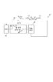
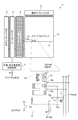
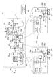
- FIG. 1 is a diagram schematically showing an A / D conversion integrated circuit according to the present embodiment.
- FIG. 2 is a drawing schematically showing a configuration of an A / D converter different from the A / D converter.
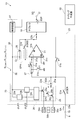
- FIG. 3 is a diagram schematically showing the A / D converter according to the present embodiment.
- FIG. 4 is a diagram showing an example of an RTZ waveform generation circuit.
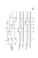
- FIG. 5 is a diagram illustrating an example of an RTZ signal receiving circuit. 6 shows output values (0, 1, 2), digital signals (D 0 , D 1 ), latch signals (B 0 , B 1 ), and control signals ⁇ D0 , ⁇ D1 , sub A / D conversion circuits, It is drawing which shows the corresponding
- FIG. 1 is a diagram schematically showing an A / D conversion integrated circuit according to the present embodiment.
- FIG. 2 is a drawing schematically showing a configuration of an A / D converter different from the A / D converter.
- FIG. 7 is a view showing an image sensor as an example to which the A / D converter is applied.
- FIG. 8 is a diagram illustrating timing for the operation of the A / D converter according to the present embodiment.
- FIG. 9 is a drawing schematically showing a configuration of a cyclic A / D converter.
- FIG. 10 is a timing chart showing the operation of the cyclic A / D converter shown in FIG.
- FIG. 11 is a diagram illustrating waveforms of control signals for controlling a D / A conversion circuit that provides a binary signal SDA.
- FIG. 12 is a diagram illustrating waveforms of control signals for controlling a D / A conversion circuit that provides a binary signal SDA.
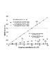
- Figure 13 is a graph showing the results of simulation of the error that occurs when the coupling between the virtual ground point parasitic capacitor C C in the interior of the amplifier circuit of the cyclic A / D converter has occurred.
- FIG. 14 is a drawing schematically showing a configuration of another A / D converter.
- FIG. 1 is a diagram schematically showing an A / D conversion integrated circuit according to the present embodiment.
- the A / D conversion integrated circuit 11 includes a plurality of A / D converters 13a to 13n.
- the array of A / D converters 13a to 13n may be arranged in accordance with a predetermined width.
- a typical A / D converter 13a the configuration of an A / D converter (referred to as "13") is shown.
- the A / D converter 13 includes an input 15, an output 17, a sub A / D conversion circuit 19, a control circuit 21, and a signal processing circuit 23.
- Input 15 receives an analog signal SA to be A / D converted.
- the output 17 provides at least a portion (eg, a sub-digital signal) of the digital signal SD having a predetermined number of bits representing the analog signal SA.
- the sub A / D conversion circuit 19 receives the analog signal SA, generates a signal SDP representing one or more bit values of the digital signal SD, and provides the signal SDP to the output 17.
- the input 21a of the control circuit 21 is connected to the output 19a of the sub A / D conversion circuit 19, and provides a first control signal S CONT according to the signal SDP.
- the first control signal S CONT has a waveform including a transition from the first voltage level L1 to the second voltage level L2 and a transition from the second voltage level L2 to the first voltage level L1.
- This waveform is generated by an AND gate that receives the signal SDP and the pulse signal SP, for example.
- the pulse width of the control signal S CONT is defined by the signal SP.
- the control signal S CONT can also be generated by a multiplexer, and the multiplex receives a signal SP having several pulse widths, whereby the control signal S CONT has the value of the signal SDP. Pulse width can be specified.
- the D / A conversion circuit 25 and the storage circuit 33 constitute a D / A converter 26.
- the D / A converter 26 is connected to the output 21 b of the control circuit 21.
- the signal processing circuit 23 includes a first capacitor 27, a second capacitor 29, and an operational amplifier circuit 31.
- the D / A converter 26 includes a storage circuit 33 and a D / A conversion circuit 25.
- the memory circuit 33 latches the first control signal S CONT from the control circuit 21 in response to the signal ⁇ LAT0.
- the D / A conversion circuit 25 provides an analog output value SDA corresponding to the stored value of the storage circuit 33.
- the signal processing circuit 23 connects a first capacitor 27 between an input of a switched-capacitor amplifier circuit 20 and a first input (for example, an inverting input) 31a of the operational amplifier circuit 31 and an operational amplifier circuit. Signal processing is performed by connecting a second capacitor 29 between an output 31 (for example, non-inverted output) 31b and a first input (for example, inverted input) 31a.
- the connection of the first and second capacitors 27 and 29 and the operational amplifier circuit 31 constitutes an SC amplifier.
- the input 31a is a virtual ground and can be called a virtual ground terminal.
- the second input (for example, non-inverting input) 31c of the operational amplifier circuit 31 is connected to the ground line.
- an operation value is generated at the output (eg, non-inverted output) 31b of the operational amplifier circuit 31.
- This calculated value is provided to the output of the signal processing circuit 23.
- the signal processing circuit 23 connects the second capacitor 29 between the output 31 b of the operational amplifier circuit 31 and the first input (for example, inverting input) 31 a and connects the first capacitor 27 from the operational amplifier circuit 31. Separately, a signal holding process for holding the voltage in the second capacitor 29 is performed.
- the input 31 a of the operational amplifier circuit 31 is connected in the A / D converter 13 in the operation mode in which at least one of the capacitors 27 and 29 is connected to the input (for example, the input 31 a) of the operational amplifier circuit 31, the input 31 a of the operational amplifier circuit 31 is connected.
- the impedance of the connected node (conductor region) is not sufficiently low. Therefore, it is sensitive to noise. Since the signal processing circuit 23 processes an analog signal, the noise to the above node hinders improvement in the accuracy of A / D conversion
- each of the A / D converters 13a to 13n is laid out with a small size (width).
- the arrangement and wiring of the components of the A / D converter are provided with high density.
- the first input 31a of the operational amplifier circuit 31, one end of the first capacitor 27, and one end of the second capacitor 29 are connected to each other to form a conductive region EPR.
- the second capacitor 29 is connected between the output 31b of the operational amplifier circuit 31 and the first input 31a, and the first capacitor 27 is connected from the operational amplifier circuit 31.
- the conductive region EPR may be formed by being separated. During signal processing, the conductive region EPR is equipotential.
- the first control signal S CONT propagates on the conductor 35 that connects the storage circuit 33 of the D / A converter 26 and the control circuit 21. In the limited layout described above, the conductor 35 passes near the conductor region EPR.
- the signal processing in the signal processing circuit 23 uses the connection constituting the SC amplifier. Therefore, the first input 31a of the operational amplifier circuit 31 is coupled with another conductor (for example, the conductor 35) connected to the signal processing circuit 23 through a parasitic capacitor. Therefore, the conductor region EPR equipotential with the first input 31a of the operational amplifier circuit 31 exhibits a high impedance.
- the operation of the D / A conversion circuit 25 is controlled by the control circuit 21.
- the first control signal S CONT is given from the control circuit 21 to the D / A conversion circuit 25.
- the waveform of the first control signal S CONT includes two transitions between L1 and L2 to the first and second voltage levels, so that the first control signal S CONT is another conductor (eg, conductor EPR).
- the noise given is based on two transitions in opposite directions. Therefore, when other conductors that receive noise (for example, conductor EPR) have high impedance, noise based on two opposite transitions (or the same number of transitions opposite to each other and zero or more) is the result. Canceled.
- the input from the operational amplifier circuit 31 to which the first and second capacitors 27 and 29 are connected is in a high-impedance state, for example, DC and AC, from the first voltage level L1 to the second voltage level L2.
- the first control signal S CONT has a waveform in which the transition and the transition from the second voltage level L2 to the first voltage level L1 include the same number of transitions.
- the D / A converter 26 includes a storage circuit 33 that latches the first control signal S CONT, and the output 25 a of the D / A conversion circuit 25 provides an output value corresponding to the stored value of the storage circuit 33. Therefore, the D / A conversion circuit 25 can be operated by the control signal S CONT having a waveform having two transitions.
- the first control signal S CONT propagates through the conductor 35, and the conductor 35 is supplied to the conductor region EPR connected to the first input 31a of the operational amplifier circuit 31 at the time of signal processing. It is capacitively coupled through a parasitic capacitor C C.
- the parasitic capacitor C C regardless of the size of the capacitive coupling through the parasitic capacitor C C (In a real circuit, to estimate the specific size of the parasitic capacitor C C
- the noise based on the two transitions opposite to each other is canceled as a result.
- FIG. 2 is a drawing schematically showing a configuration of an A / D converter different from the A / D converter 13.
- the signal V CONV for controlling the D / A conversion circuit 43 is provided from the sub A / D conversion circuit 45 via the conductor 44.
- This signal V CONV has a single transition from the first voltage level L1 to the second voltage level L2, or a single transition from the second voltage level L2 to the first voltage level L1.
- the SC amplifier when the conductor EPR receiving noise has a high impedance, the noise based on a single transition is not canceled.
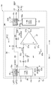
- FIG. 3 is a drawing schematically showing an A / D converter according to the present embodiment.
- the A / D converter 14 can be replaced with individual A / D converters 13a to 13n in the array of A / D converters 13a to 13n shown in FIG.
- the A / D converter 14 includes an input 15, an output 17, a sub A / D conversion circuit 19, an RTZ waveform generation circuit 22, a D / A conversion circuit 25, a switch capacitor amplification circuit 20, and an RTZ signal reception. Circuit 18.
- the RTZ waveform generation circuit 22 has an input 22a connected to the output 19a of the sub A / D conversion circuit 19, and modulates the signal SDP from the output of the sub A / D conversion circuit 19 to return to zero ( RTZ) A signal RTZ is generated.
- the RTZ signal receiving circuit 18 has an input 18a that receives the return-to-zero signal RTZ from the output 22a of the RTZ waveform generating circuit 22, and generates a digital signal that encodes the return-to-zero signal RTZ.
- This digital signal is stored in a storage circuit in the RTZ signal receiving circuit 18. The stored value of this storage circuit is provided to the D / A conversion circuit 25 via the output 18b of the RTZ signal reception circuit 18.
- the switch capacitor amplifier circuit 20 includes a plurality of capacitors 27 and 29, switch elements 32 a, 32 b, 32 c, 32 d, and 32 e and an operational amplifier circuit 31.
- the switch capacitor amplifier circuit 20 at least one of the capacitors 27 and 29 (in this embodiment, the capacitor 27) is connected to a virtual ground terminal (for example, 31a) of the operational amplifier circuit 31 via a switch element (for example, 32c). Connected.
- Timing generating circuit 34 timing signals ⁇ 1, ⁇ 2, ⁇ CDS1 , generates phi CDS2, switching elements 32a ⁇ 32e, these timing signals ⁇ 1, ⁇ 2, ⁇ CDS1 , ⁇ CDS2, controlled by phi DAC
- the RTZ signal receiving circuit 18 encodes a digital value from the return-to-zero signal RTZ from the output 22 a of the RTZ waveform generation circuit 22. This encoded signal has a value for controlling the D / A conversion circuit 25 and is held in a storage circuit in the RTZ signal receiving circuit 18.
- the memory circuit in the RTZ signal receiving circuit 18 may store the return-to-zero signal RTZ from the output 22a of the RTZ waveform generating circuit 22, and the RTZ signal receiving circuit 18 may digitally convert the signal from the signal in the memory circuit. Generate a value.
- the D / A conversion circuit 25 provides an analog output value SDA.
- the D / A conversion circuit 25 provides an analog output value SDA corresponding to the stored value of the storage circuit.
- the connection of the first and second capacitors 27 and 29 and the operational amplifier circuit 31 constitutes an SC amplifier. In this SC amplifier, the second input (for example, non-inverting input) 31c of the operational amplifier circuit 31 is connected to the ground line.
- the signal processing circuit 24 connects the first capacitor 27 between the input of the switched capacitor amplifier circuit 20 and the first input (for example, inverting input) 31a of the operational amplifier circuit 31, and outputs the output (for example, the operational amplifier circuit 31).
- a second capacitor 29 is connected between the non-inverted output) 31b and the first input (for example, inverted input) 31a to perform signal processing.
- an operation value is generated at the output 31 b of the operational amplifier circuit 31. This calculated value is provided to the output of the signal processing circuit 24.
- the first input (for example, the inverting input) 31a is connected to one end of the capacitors 27 and 29, and the conductor region equipotential to the potential of these connection nodes does not have a sufficiently low impedance.
- Conductive regions, such as potential connected to the input 31a of the operational amplifier 31 is coupled through a parasitic capacitor C C from the output 22b of the RTZ waveform generator circuit 22 to the wiring conductor 36 to the input 18a of the RTZ signal receiving circuit 18
- the Potential change on the wiring conductor 36 is transmitted to the conductor of the equipotential through the parasitic capacitor C C.
- the return-to-zero signal RTZ propagates through the wiring conductor 36, and the return-to-zero signal RTZ has two transitions in opposite directions.
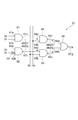
- FIG. 4 is a diagram showing one circuit example of the RTZ waveform generation circuit 22.
- the RTZ waveform generation circuit 22 receives a signal SDP (D 0 , D 1 ) from the output of the sub A / D conversion circuit 19.
- the RTZ waveform generation circuit 22 can generate the return-to-zero signal RTZ by modulating the signal SDP.
- the signals D 0 and D 1 are received by a plurality of logic gates, for example, AND (logical product) gates 61 and 62.
- the inputs 61a and 61b of the AND gate 61 receive the signals D 0 and D 1
- the inputs 62a and 62b of the AND gate 62 receive the signals D 0 and _D 1 .
- the signal _D 1 indicates an inverted signal of the signal D 1 .
- an inverter 63 can be connected to the input 62b of the AND gate 62 to generate the inverted signal.
- the input 64a of the AND gate 64 receives the logical product signal AND1 from the output 61c of the AND gate 61, and the input 64b of the AND gate 64 receives the signal W2.
- An input 65a of the AND gate 65 receives a logical product signal AND2 from an output 62c of the AND gate 62, and an input 65b of the AND gate 65 receives a signal W1.
- Inputs 66a and 66b of an exclusive OR (EXOR) gate 66 receive logical product signals AND3 and AND4 from outputs 64c and 65c of AND gates 64 and 65, respectively.
- the exclusive OR gate 66 generates a return-to-zero signal RTZ.
- the signals W1 and W2 are signals for generating image data, and are provided from the 1.5b sub A / D conversion circuit.
- FIG. 5 is a circuit diagram showing an example of the RTZ signal receiving circuit 18 and the D / A conversion circuit 25.
- the RTZ signal receiving circuit 18 stores the return-to-zero signal RTZ from the output 22b of the RTZ waveform generation circuit 22 and encodes a digital value from the return-to-zero signal RTZ.
- the RTZ signal receiving circuit 18 includes a storage circuit 71 and an encoder 81.
- a memory circuit 71 is shown in part (a) of FIG.
- the storage circuit 71 can include a storage circuit capable of storing one or a plurality of bits. In this embodiment, the storage circuit 71 includes latch circuits 72 and 73.
- the return-to-zero signal RTZ is provided to the latch circuits 72 and 73 via the wiring conductor 36 connected to the inputs 72a and 73a of the latch circuits 72 and 73.
- the latch signals LAT1 and LAT2 are input to the latch inputs 72b and 73b of the latch circuits 72 and 73, respectively, and define the latch timing of the latch circuits 72 and 73.
- the latch circuits 72 and 73 store values B 0 and B 1 defined by the latch signals LAT1 and LAT2, respectively, and provide these stored values to the outputs 72c and 73c.
- the encoder 81 includes logic gates such as a plurality of AND gates. For example, in order to encode the 2-bit signals B 0 and B 1 , four AND gates are necessary, but in the present A / D conversion circuit 14, 1.5-bit A / D conversion is performed for each cycle. Therefore, control signals ⁇ D0 , ⁇ D1 , and ⁇ D2 are generated by encoding using the three AND gates 82, 83, and 84.
- the signal ⁇ DAC defines the timing for supplying the control signal to the D / A conversion circuit 25. Inputs 82c, 83c, 84c of AND gates 82, 83, 84 receive signal ⁇ DAC.
- Inputs 82a and 82b of AND gate 82 receive signals B 0 and B 1 , respectively.
- the inputs 83a and 83b of the AND gate 83 receive signals B 0 and _B 1 respectively.
- the inputs 84a and 84b of the AND gate 83 receive the signals _B 0 and _B 1 respectively.
- an inverter 85 is used at the input of the necessary AND gate.
- outputs 82d, 83d, and 84d of AND gates 82, 83, and 84 provide control signals ⁇ D0, ⁇ D1, and ⁇ D2, respectively.
- control signals ⁇ D0, ⁇ D1, and ⁇ D2 control the three switch elements 86a, 86b, and 86c in the D / A conversion circuit 25.
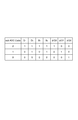
- List of output values (0, 1, 2), digital signals (D 0 , D 1 ), latch signals (B 0 , B 1 ), and control signals ⁇ D 0 , ⁇ D 1, ⁇ D 2 of the sub A / D conversion circuit 19 Is shown in FIG.
- FIG. 7 is a diagram showing an image sensor as an example to which the A / D converter is applied.
- the sensor array 2 includes an array of sensor circuits 2a including sensor elements.
- a vertical shift register 3 is connected to a row of the sensor array 2
- an A / D converter array 4 is connected to a column of the sensor array 2.
- the A / D converter array 4 includes a plurality of A / D converters 13 arranged in an array on the column of the image sensor.
- the A / D converter array 4 is arranged in accordance with the width of the column of the sensor array 2.
- the number of A / D converters 13 is equal to the number of column lines.
- the individual A / D converters 13 are laid out according to the cell size in the sensor array 2.
- the sensor array 2 includes sensor circuits 2 a of the CMOS image sensor arranged in the row direction and the column direction.
- FIG. 7 shows a pixel PIXEL of the CMOS image sensor, and the pixel PIXEL is an example of the sensor circuit 2a.
- the application of the A / D converter 13 according to the present embodiment is not limited to the specific configuration described in this specification.
- the sensor circuit described above is not limited to an image sensor, but can be applied to various sensors that can be integrated together in a semiconductor circuit in addition to the pixel PIXEL.
- Examples of applicable sensors include a distance sensor, a magnetic sensor, an acceleration sensor, and a pressure sensor.
- the configuration of the CMOS image sensor 1 will be described with reference to FIG.
- the pixel PIXEL generates a first signal S1 in the reset state and a second signal S2 in the light induced signal output.
- An input 13 of the A / D converter 11 is connected to the pixel PIXEL.
- a data register 5 is connected to the A / D converter array 4, and an A / D conversion value corresponding to a signal from the pixel PIXEL is stored in the data register 5.
- the data register 5 provides the digital signal to the redundant representation / non-redundant representation conversion circuit 7 in response to the signal from the horizontal shift register 6.
- the redundant expression / non-redundant expression conversion circuit 7 generates an N-bit digital code corresponding to the signal from the pixel PIXEL.
- the photodiode DF receives light for one pixel related to the image (Optical Signal).
- the gate of the selection transistor M S is connected to the row select line S extending in the row direction.
- the gate of the reset transistor M R is connected to the reset line R.
- the gate of the transfer transistor M T is connected to the transfer selection line extending in the row direction.
- One end of the photodiode D F is connected to the floating diffusion layer FD via the transfer transistor M T.
- Floating diffusion layer FD is connected to a reset potential line Reset via the reset transistor M R, is connected to the gate of the transistor M A.
- One current terminal (for example, source) of the transistor M A is connected to the column line 8 via the selection transistor M S.
- Transistor M A is provided in the column line through the selection transistor M S a potential corresponding to the charge amount of the floating diffusion layer FD.
- the noise canceling operation is performed as follows. First, to provide a reset control signal R to the reset transistor M R, it resets the floating diffusion layer FD. Through the amplification transistor M A, read out the reset level. The pixel PIXEL generates the first signal S1 when the floating diffusion layer FD is in the reset state. Then, a charge transfer control signal TX is supplied to the transfer transistor M T, is transferred from the photodiode D F photoinduced signal charges to the floating diffusion layer FD. Thereafter, this signal level is read out through the transistor MA. The second signal S2 is generated when the floating diffusion layer FD of the pixel PIXEL is in a photo-induced charge accumulation state.
- the first signal S1 is superimposed on the signal indicating the photoinduced charge.
- the difference between the reset level and the signal level is obtained using an A / D converter as shown in FIG.
- noise such as fixed pattern noise due to variations in the characteristics of the transistors of the pixel PIXEL and reset noise generated when the floating diffusion layer is reset are canceled.
- FIG. 8 is a diagram illustrating timing for the operation of the A / D converter according to the present embodiment. The operation of the A / D converter will be described with reference to FIGS.
- FIG. 8 is a diagram showing an analog CDS operation and an A / D conversion operation in the first three cycles CYC1, CYC2, and CYC3. During the period when both of the timing signals ⁇ CDS1 and ⁇ CDS2 are “high”, the signal S1 is received from the sensor circuit 2a and stored in the capacitor 27.
- the signal S2 from the sensor circuit 2a is received and the analog CDS operation is performed in the SC amplifier of the signal processing circuit 23 to obtain the difference.
- the signal (S1-S2) is generated at the output 31b of the operational amplifier circuit 31.
- the sub A / D conversion circuit 19 generates an A / D conversion signal SDP of this signal.
- the RTZ waveform generation circuit 22 receives the signal SDP (D 0 , D 1 ) from the output of the sub A / D conversion circuit 19 and generates a return-to-zero signal RTZ 1 from the signal SDP. This signal RTZ 1 propagates through the conductor wiring 36 and reaches the RTZ signal receiving circuit 18.
- the storage circuit 71 stores the digital values (B 0 , B 1 ) in response to the latch signals LAT1 and LAT2.
- the RTZ waveform generation circuit 22 receives the signal SDP (D 0 , D 1 ) from the output of the sub A / D conversion circuit 19 and generates a return-to-zero signal RTZ 2 from the signal SDP. This signal RTZ 2 propagates through the conductor wiring 36 and reaches the RTZ signal receiving circuit 18.
- the storage circuit 71 stores the digital values (B 0 , B 1 ) in response to the latch signals LAT1 and LAT2.
- the RTZ waveform generation circuit 22 receives the signal SDP (D 0 , D 1 ) from the output of the sub A / D conversion circuit 19 and generates a return-to-zero signal RTZ 3 from the signal SDP. This signal RTZ 3 propagates through the conductor wiring 36 and reaches the RTZ signal receiving circuit 18.
- the storage circuit 71 stores the digital values (B 0 , B 1 ) in response to the latch signals LAT1 and LAT2.
- the cyclic A / D conversion operation includes a cyclic operation mode and an arithmetic processing mode.
- each cycle A / D conversion cycle CYC1, CYC2, CYC3 during the period when the signal ⁇ 1 is high and the signal ⁇ 2 is low in FIG. 8, the capacitor 27 is connected via the analog signal from the input 15 or the switch 32a.
- Receive feedback value (cyclic operation mode).
- One end and the other end of the capacitor 29 are respectively connected to the input 31a and the output 31b of the operational amplifier circuit 31, and the capacitor 27 is disconnected from the input 31a of the operational amplifier circuit 31 by a switch 32c.
- the impedance of the conductor to which the input 31a of the operational amplifier circuit 31 is connected is high.
- a node to which the capacitor 29 and the input 31a are connected holds a potential.
- the capacitors 27 and 29 are connected to the input 31a of the operational amplifier circuit 31.
- the SC amplifier performs an operation (arithmetic processing mode).
- the capacitors 27 and 29 are connected to the input 31a of the operational amplifier circuit 31, and one end and the other end of the capacitor 29 are connected to the input 31a and the output 31b of the operational amplifier circuit 31, respectively.
- the impedance of the conductor to which the input 31a of the operational amplifier circuit 31 is connected is high.
- the node to which the capacitors 27 and 29 are connected holds the potential.
- the virtual ground terminal (here, the input 31a) of the operational amplifier circuit 31 is in the virtual ground state.
- a return-to-zero signal is sent from the sub A / D conversion circuit 19 to the D / A conversion circuit 25 in the cyclic operation mode. If necessary, a return-to-zero signal can be sent early in the processing mode.
- the length of the high-state period of the return-to-zero signal RTZ1 is different from the length of the high-state period of the return-to-zero signal RTZ2, and similarly, the length of the high-state period of the return-to-zero signal RTZ1 is the return-to-zero signal RTZ3. Different from the high period length (zero length).
- Such return-to-zero signals RTZ1, RTZ2, and RTZ3 propagate through the conductor wiring 36 and reach the RTZ signal receiving circuit 18.
- the switch capacitor amplifier circuit 20 processes the analog signal for the A / D conversion. Return-to-zero signal RTZ is propagated through the conductor wiring 36, the conductive wire 36 is attached via a parasitic capacitor C C and the nodes in the switched capacitor amplifier circuit 20.
- the node of the switched capacitor amplifier circuit 20 may be subject to disturbance from the conductor wire 36 via the parasitic capacitor C C.
- the return-to-zero signal RTZ1, RTZ2, digital transition RTZ3 propagates as noise to the node via the parasitic capacitor C C.
- all of the return-to-zero signals RTZ1, RTZ2, and RTZ3 have zero or even number of transitions (the transition from the first voltage value L to the second voltage value H and the second voltage value H to the first voltage value). Transition of the voltage value of 1 to L), the noise of the first transition is substantially canceled by the noise of the reverse polarity of the second transition.
- the resulting residual noise is very small.
- FIG. 9 is a drawing schematically showing a configuration of a cyclic A / D converter.
- a / D conversion is performed one or several bits less than the total number of digital bits. For example, A / D conversion for several bits of an analog signal is performed, and a signal corresponding to these bit values is subtracted using an operational amplifier circuit to generate a calculation value. A / D conversion of the calculated value is performed, and a signal corresponding to the converted bit value is subtracted using an operational amplifier circuit to generate a calculated value for the next cyclic operation. This is repeated until a digital signal having a desired number of bits is obtained.
- the D / A conversion circuit 25 is closer to the sensor array 2 than the sub A / D conversion circuit 19.
- the signal processing circuit 23 connects the second capacitor 29 between the output 31b of the operational amplifier circuit 31 and the input 31a of the operational amplifier circuit 31, and disconnects the first capacitor 27 from the input 31a.
- the first capacitor 27 receives an analog value via the input 15 or the switch 51b, and the second capacitor 29 holds the analog value (potential) at the input 31a.
- the signal processing circuit 23 has a first capacitor 27 connected between the input 23a of the signal processing circuit 23 or the output 25a of the D / A conversion circuit 25 and the input 31a of the operational amplifier circuit 31 and an operational amplifier circuit.
- the second capacitor 29 is connected between the output 31b of the circuit 31 and the input 31a of the operational amplifier circuit 31 to perform signal processing.
- the input 23a is connected to one end of the first capacitor 27 via the switch 51a.
- the cyclic A / D converter includes a feedback path that feeds back an operation value generated by signal processing from the output 31b of the operational amplifier circuit 31 to the input of the SC amplifier.
- This feedback path includes a switch 51b.
- the sub A / D converter circuit 19 is arranged near the output of the A / D converter 13.
- the conductor 35 for the control signal extends from the output side of the A / D converter 13 toward the input side.
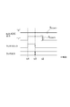
- FIG. 10 is a timing chart showing the operation of the cyclic A / D converter shown in FIG.
- the cyclic A / D converter 13 shown in FIG. 9 performs 1.5-bit A / D conversion in one cyclic operation.
- the D / A conversion circuit 25 provides three analog values (for example, + V R , zero, ⁇ V R ).
- the D / A conversion circuit 25 includes three switches 26a, 26b, and 26c, and these switches 26a, 26b, and 26c operate in response to the control signal.
- Three reference signals (+ V R , zero, ⁇ V R ) are provided by voltage sources 30a, 30b, 30c.
- the memory circuit 33 includes storage circuits 33a and 33b such as a latch circuit that stores three control signals.
- the storage circuits 33a and 33b store control signals and hold stored values in response to the storage signals ⁇ LAT1 and ⁇ LAT2, respectively.
- the control circuit 21 generates control signals S CONT1 , S CONT2 , and S CONT3 for generating a ternary D / A signal SDA.
- the switches 51a, 51b, 51c, 51d, 51e respond to signals provided by the timing generator 50.
- the cyclic A / D converter 13 performs a reset operation prior to receiving an analog signal via the input 15. In the reset operation, the switches 51d and 51e are closed in response to the signals ⁇ CDS2 and ⁇ 2.
- the cyclic A / D converter 13 a receives the analog signal SA via the input 15.
- the switch 51a is closed in response to the signal ⁇ CDS1, and the switches 51b and 51c are closed in response to the signal ⁇ 1.
- the switch 51d is opened in response to the signal ⁇ CDS2, and the switch 51e is opened in response to the signal ⁇ 2.
- the analog signal SA is stored in the capacitor 27. At this time, the output of the D / A conversion circuit 25 is in a high impedance state (HiZ).
- the output 31b of the operational amplifier circuit 31 is connected to the input 31a of the operational amplifier circuit 31 via the capacitor 29. With this connection, in the SC amplifier, the conductor region to which the input 31a is connected has a sufficiently low impedance. Absent.
- the analog signal SA is provided to the sub A / D conversion circuit 19 via the switch 51b, and the sub A / D conversion circuit 19 generates a partial A / D conversion value SDP for 2 bits.
- the sub A / D conversion circuit 19 includes, for example, two comparators, and provides the comparison results of the individual comparators as A / D conversion values SDP. The two comparators receive reference values + V R and ⁇ V R , respectively.
- the signal processing circuit 23 After taking in the analog signal, the signal processing circuit 23 opens the switches 51a and 51d in response to the signals ⁇ CDS1 and ⁇ CDS2, and opens the switches 51b and 51c in response to the signal ⁇ 1. In response to the signal ⁇ 2, the switch 51e is closed.
- the capacitors 27 and 29 and the operational amplifier circuit 31 constitute an SC amplifier.
- the conductor region EPR is connected to the virtual ground terminal of the operational amplifier circuit 31, also a high impedance node, also are capacitively coupled through a parasitic capacitor C C to the conductor 35.
- control circuit 21 generates a signal (any one of the control signals S CONT1 , S CONT2 , S CONT3 ) corresponding to the received A / D conversion value SDP. This signal propagates on the conductor 35 and reaches the memory circuit 33.
- the transmission period of the control signals S CONT1 , S CONT2 and S CONT3 is within a period in which the SC amplifier is constituted by the capacitors 27 and 29 and the operational amplifier circuit 31. During this period, the conductor region EPR is placed in a high impedance state in terms of alternating current and direct current.
- the start of the transmission period is after the start of the operation period of the SC amplifier, and the end of the transmission period is before the end of the operation period of the SC amplifier.
- the control signal S CONT1 has the longest duration and causes the second transition T2 at time t2.
- the control signal S CONT2 has the next longest duration and causes the second transition T2 at time t3.
- the control signal S CONT3 has the shortest duration and causes the second transition T2 at time t4.
- the latch timing of the storage circuit 33a is defined by the signal ⁇ LAT1, and the stored value of the storage circuit 33a is determined at time t5.
- the latch timing of the storage circuit 33b is defined by the signal ⁇ LAT2, and the stored value of the storage circuit 33b is determined at time t6. Second transition T2 of the control signal S CONT1 precedes the time t5, the second transition T2 of the control signal S CONT2 is located before time t6.
- the stored value of the storage circuit 33a is determined at time t5, and the stored value is “1”.
- the stored value of the storage circuit 33b is determined at time t6, and the stored value is “1”.
- the control circuit 21 provides the control signal S CONT2 , the stored value of the storage circuit 33a is determined at time t5, and the stored value is “1”.
- the stored value of the storage circuit 33b is determined at time t6, and the stored value is “0”.
- the control circuit 21 provides the control signal S CONT3
- the stored value of the storage circuit 33a is determined at time t5, and the stored value is “0”.
- the stored value of the storage circuit 33b is determined at time t6, and the stored value is “0”.
- the stored values of the storage circuits 33a and 33b are converted into switch signals for controlling the opening / closing of the switches 26a to 26c, for example, by the decoder circuit 33c.
- any one of the switches 26a-26c couples the signal SDA to one end of the capacitor 27.
- an operation value by the first cyclic operation is generated.
- This calculated value is provided to the output 17 by the sub A / D conversion circuit 19 as the second signal SDP. Further, the signal SDP is provided to the control circuit 21, and a control signal (any one of the control signals S CONT1 , S CONT2 , S CONT3 ) for the second cyclic operation is generated. This control signal is stored in the memory circuit 33 after propagating through the conductor 35.
- the D / A conversion circuit 25 provides a signal SDA corresponding to the stored value of the storage circuit 33 to one end of the capacitor 27. The cyclic A / D conversion operation is repeated until a digital signal having a desired number of bits is obtained.
- the control signal from the control circuit 21 to the storage circuit 33 has a waveform composed of two transitions in any case, so that noise based on the two transitions is canceled as a result. Is done. As a result, noise to the conductor region EPR of the SC amplifier is reduced.
- a ternary digital value (1.5 bits) is generated in one cyclic A / D conversion. It is also possible to generate a binary digital value (1 bit) in one cyclic A / D conversion. In this A / D conversion, the D / A conversion circuit 25 provides two signals SDA.
- the memory circuit 33 includes one storage circuit.
- FIG. 11 is a diagram illustrating waveforms of control signals for controlling a D / A conversion circuit that provides a binary signal SDA. Although all of the control signals S CONT1 and S CONT2 are described in the timing chart of FIG. 11, the signal generated in each cyclic operation is any one of them. When the signal is generated, both of the control signals S CONT1 and S CONT2 cause the first transition T1 at time s1 at the timing of the cyclic operation. Control signal S CONT1 has a long duration, causing a second transition T2 at time s2. The control signal S CONT2 has a short duration and causes a second transition T2 at time s3.
- the storage timing of the single storage circuit is defined by the latch clock signal, and the storage value of this storage circuit is determined at time s4.
- the second transition T2 of the control signal S CONT1 is located before the time s4.
- the stored value of the storage circuit is determined at time s4, the stored value is “1”, and when the control circuit 21 provides the control signal S CONT2 , the stored value is stored.
- the stored value of the circuit is determined at time s4, and the stored value is “0”.
- FIG. 12 is a diagram illustrating waveforms of control signals for controlling a D / A conversion circuit that provides a binary signal SDA.
- the control signals S CONT1 and S CONT2 are described in the timing chart of FIG. 12, the signal generated in each cyclic operation is any one of them.
- the control signal S CONT2 is a signal having no value and having a constant value.
- the control signal S CONT1 causes the first transition T1 at time u1 at the timing of the cyclic operation.
- the control signal S CONT1 causes a second transition T2 at time u2.
- the storage timing of a single storage circuit is defined by a latch clock signal, and the storage value of this storage circuit is determined at time u3.
- the stored value of the storage circuit is determined at time u3, the stored value is “1”, and when the control circuit 21 provides the control signal S CONT2 , the stored value is stored.
- the stored value of the circuit is determined at time u3, and the stored value is “0”.
- the input of the operational amplifier circuit 31 to which the capacitors 27 and 29 are connected or the input of the operational amplifier circuit 31 to which at least one of the capacitors 27 and 29 is connected is DC and Transition in which the number of transitions from the first voltage level to the second voltage level is the same as the number of transitions from the second voltage level to the first voltage level in a period in which the state is AC high impedance
- the D / A converter can be operated by a control signal having a waveform having
- the waveform of the control signal that controls the D / A conversion circuit has an even number of transitions (including zero), coupling noise due to the transition is reduced.
- noise with a voltage amplitude of about 3 millivolts (mV) is added to the conductor region EPR in a typical A / D converter due to capacitive coupling via a parasitic capacitor.
- RTZ encoding the control signal from the control circuit 21 to the D / A conversion circuit 25 both noise having a voltage amplitude of about 3 millivolts and noise having a voltage amplitude of about -3 millivolts are applied to the potential region EPR.
- a noise level of 3 mV corresponds to 12 LEB.
- the noise level 3 mV is a large value.
- FIG. 13 shows a wiring for a control signal from the comparator in the sub A / D conversion circuit to the D / A conversion circuit in an amplification circuit (MDAC: Multiplying D / A converter) in the cyclic A / D converter.
- MDAC Multiplying D / A converter
- Errors by simulation are listed for each of when the operational amplifier circuit 31 is a fully differential circuit and when it is a single-ended circuit. In either case, the effect of noise was greatly improved in accuracy by using RTZ coding. In the single-ended circuit, the influence of noise was reduced to about 1/30. By using RTZ coding in a fully differential circuit, computation for signal processing can be performed with almost no influence of errors due to coupling noise.
- FIG. 14 is a drawing schematically showing the configuration of another A / D converter.
- the sub A / D conversion circuit 19 generates an A / D conversion value of one or several bits smaller than the total number of digital bits. For example, A / D conversion for several bits of an analog signal is performed, and signals corresponding to these bit values are subtracted using an operational amplifier circuit to generate a calculated value SAR indicating a residual. The calculated value SAR is held in the hold circuit 61.
- the sub A / D conversion circuit 19 is located closer to the sensor array 2 than the D / A conversion circuit 25. In the A / D converter 13, the sub A / D conversion circuit 19 is disposed near the input of the A / D converter 13.
- a conductor for the control signal (conductor 35 in FIG. 1) extends from the input side to the output side of the A / D converter 13.
- the signal processing circuit 23 includes a D / A converter 26, capacitors 27, 27 a and 27 b, and an operational amplifier circuit 31.
- the D / A converter 26 includes first and second D / A converters 28a and 28b.
- Each of the first and second / A converters 28a and 28b includes a D / A converter circuit 25 and a memory.
- a circuit 33 is included.
- Each of the first and second / A converters 28a and 28b is connected to voltage sources 30d and 30e in order to provide a D / A value.
- one end of the capacitor 27 is connected to one end of the capacitor 29 and the first input 31a of the operational amplifier circuit 31 to form a conductor region EPR.
- one end of the capacitor 27 is disconnected from the input 31a of the operational amplifier circuit 31 and one end of the capacitor 29 is connected to the input 31a of the operational amplifier circuit 31 to form the conductor region EPR.
- the signal processing circuit 23 includes one or a plurality of switches controlled by the timing generator 60. These switches are disposed at positions similar to the switches 51a to 51e in FIG. 9, for example. Through these switches, the capacitor 27a, the capacitor 27b, the capacitor 27, the capacitor 29, and the operational amplifier circuit 31 can be connected.
- the signal processing circuit 23 constitutes an SC amplifier
- one end of the capacitor 27b, one end of the capacitor 27a, one end of the capacitor 27, one end of the capacitor 29, and the first input 31a of the operational amplifier circuit 31 are connected to each other.
- a conductor region EPR is formed.
- the output 24a of the first D / A converter 28a is connected to one end of the capacitor 27, one end of the capacitor 29, one end of the capacitor 27b, and the first of the operational amplifier circuit 31 via the capacitor (capacitance: 2C) 27a.
- the output 24b of the second D / A converter 28b is connected to one end of the capacitor 27, one end of the capacitor 29, one end of the capacitor 27a, and the first output of the operational amplifier circuit 31 via a capacitor (capacitance: C) 27b. Connected to input 31a.
- the conductor region EPR is capacitively coupled to the conductor 35, which is a propagation path of the control signal, via a parasitic capacitor.
- the operation of the A / D converter 13 shown in FIG. 14 will be described.
- the switch 63a By conducting the switch 63a in response to the signal phi R, samples the reset level signal S1 of the output signal from the sensor circuit 2a in the cell array 2 to the capacitor 27.
- the signal level signal S2 of the output signal from the sensor circuit 2a receives the capacitor 27, the signal processing using the capacitors 27, 29 and the operational amplifier circuit 31 I do.
- the signal processing at this time is generation of a differential signal (S1-S2) and amplification thereof.
- an SC amplifier is configured.
- the sub A / D conversion circuit 21 generates an A / D conversion value by calculating the difference between the reset level S1 and the signal level S2 by 2-bit A / D conversion.
- the converter 26 is controlled.
- the amplified signal is expressed by the following equation.
- VOUT 4 ⁇ (S1-S2) ⁇ D ⁇ (V R1 ⁇ V R2 )
- the amplification coefficient “4” is defined by the ratio between the capacitor 27 (capacitance: 4C) and the capacitor 29 (capacitance: C).
- V R1 and V R2 are determined so that the output of the SC amplifier and (V R1 ⁇ V R2 ) are positive values.
- a value D that has been A / D converted with 2 bits is defined as follows.
- D Input analog value range. 0: (S1-S2) ⁇ (V R1 ⁇ V R2 ) / 4. 1: (V R1 ⁇ V R2 ) / 4 ⁇ (S1-S2) ⁇ (V R1 ⁇ V R2 ) / 2. 2: (V R1 ⁇ V R2 ) / 2 ⁇ (S1-S2) ⁇ 3 ⁇ (V R1 ⁇ V R2 ) / 4. 3: 3 ⁇ (V R1 ⁇ V R2 ) / 4 ⁇ (S1-S2).
- the value D is one of four values 0, 1, 2, and 3 with respect to the output of the 2-bit A / D conversion circuit, and takes a value such that the operation value VOUT is the smallest. In other words, the A / D converter 13 operates so that the calculated value VOUT becomes that way.
- the control circuit 21 generates a control signal S CONT for controlling the first and second / A conversion units 28a and 28b in accordance with the 2-bit signal from the sub A / D conversion circuit 19.
- control signal S CONT As the control signal S CONT , the control signals S CONT1 to S CONT2 having waveforms connected in FIGS. 10 to 12 can be used. Since the waveforms of these control signals include two transitions T1 and T2, digital noise to the conductor region EPR is reduced.
- the control signal S CONT is stored in the storage circuits 33 a and 33 b in the storage circuit 33.
- the D / A conversion circuit in the first / A conversion unit 28a the D / A value V R1 or V R2 is provided to the capacitor 27a weighted according to the bit position of the A / D conversion.
- the D / A value V R1 or V R2 is provided to the capacitor 27b weighted according to the bit position of the A / D conversion.
- a / D conversion of the difference between the reset level S1 and the signal level S2 by 2-bit A / D conversion will be described.
- Signals ⁇ A, ⁇ B, ⁇ C, and ⁇ D are supplied to the switches 26d and 26e of the D / A conversion circuit 25 in the first and second D / A conversion units 28a and 28b.
- these signals ⁇ A to ⁇ D are set as follows according to the value D. D: ⁇ A, ⁇ B, ⁇ C, ⁇ D.
- Output value VOUT is sampled at the hold capacitor C S by conducting the switch 61a in response to the signal phi S, is held (stored).
- the read analog residual signal SDR is subjected to subsequent signal processing (for example, A / D conversion processing of lower bits).
- the RTZ transmission system is used as a control signal to the D / A conversion circuit regardless of whether the sub A / D conversion circuit is located on either the sensor array side or the data register side. It is effective to apply When a virtual ground point is coupled to a conductive line serving as a propagation path of a digital control signal via a parasitic capacitor in an amplifier circuit, an error occurs due to coupling noise. As described above, the influence of coupling noise can be reduced by using a control signal such as an RTZ code.
- an A / D conversion integrated circuit including a plurality of A / D converters that can reduce the propagation of noise due to capacitive coupling from a conductor that transmits a digital signal. With the goal.
- control circuit 23 ... signal processing circuit, SA ... analog signals, SD ... digital signal, S CONT ... control signal, L1, L2 ... voltage level, 22 ... RTZ waveform generator circuit, 25 ... D / A conversion circuit, 26 ... D / A Exchanger, 26a, 26b, 26c ... switch, 27, 29 ... capacitor, 28a, 28b ... D / A converter, 31 ... operational amplifier circuit, 32a, 32b, 32c, 32d, 32e ... switch element, 33 ... storage circuit , ⁇ LAT0, ⁇ LAT1, ⁇ LAT2 ... latch signal, ⁇ 1, ⁇ 2, ⁇ CDS1, ⁇ CDS2, ⁇ DAC ... timing signal, EPR ...
Landscapes
- Engineering & Computer Science (AREA)
- Theoretical Computer Science (AREA)
- Physics & Mathematics (AREA)
- Electromagnetism (AREA)
- Analogue/Digital Conversion (AREA)
Abstract
Description
VOUT=4×(S1-S2)-D×(VR1-VR2)
増幅の係数「4」は、キャパシタ27(キャパシタンス:4C)とキャパシタ29(キャパシタンス:C)との比率で規定される。SCアンプの出力及び(VR1-VR2)が正値となるようにVR1、VR2を定める。
2ビットでA/D変換された値Dは以下のように規定される。
D、 入力アナログ値の範囲。
0:(S1-S2)≦(VR1-VR2)/4。
1:(VR1-VR2)/4<(S1-S2)≦(VR1-VR2)/2。
2:(VR1-VR2)/2<(S1-S2)≦3×(VR1-VR2)/4。
3:3×(VR1-VR2)/4≦(S1-S2)。
値Dは、2ビットA/D変換回路の出力に対して、0、1、2、3の4値のいずれかとなり、演算値VOUTが最も小さくなるような値を取る。換言すれば、演算値VOUTがそのようになるように、A/D変換器13が動作する。
D:φA 、φB 、φC 、φD 。
0:1→1、0→0、1→1、0→0。
1:1→0、0→1、1→1、0→0。
2:1→1、0→0、1→0、0→1。
3:1→0、0→1、1→0、0→1。
このような動作により、信号処理回路23における出力値VOUTが生成される。
Claims (15)
- 複数のA/D変換器を含むA/D変換集積回路であって、
各A/D変換器は、
A/D変換されるべきアナログ信号を受ける入力と、
該アナログ信号を表す所定ビット数のデジタル信号の少なくとも一部分を提供する出力と、
前記アナログ信号を受けて前記デジタル信号のうちの一又は複数のビット値を表すサブデジタル信号を生成すると共に、該サブデジタル信号を前記出力に提供するサブA/D変換回路と、
前記サブA/D変換回路の出力に接続され、前記サブデジタル信号を変調したRTZ信号を発生するRTZ波形発生回路と、
D/A変換回路と、
複数のキャパシタ、スイッチ素子及び演算増幅回路からなり、少なくとも前記キャパシタの1つが前記演算増幅回路の仮想接地端子に前記スイッチ素子を介して接続されてなるスイッチキャパシタ増幅回路と、
前記RTZ信号をデジタル信号にエンコードした信号を保持する記憶回路を備え、前記記憶回路の出力を前記D/A変換回路に出力するRTZ信号受信回路と、
を備えたA/D変換集積回路。 - 前記RTZ波形発生回路の前記RTZ信号は、前記演算増幅回路の仮想接地端子に接続される前記スイッチ素子の状態が変化しない期間において、第1の電圧レベルから第2の電圧レベルへの遷移と前記第2の電圧レベルから前記第1の電圧レベルへの遷移とが同数の遷移数を含む波形からなる、請求項1に記載されたA/D変換集積回路。
- 前記RTZ波形発生回路の前記RTZ信号は、前記演算増幅回路の仮想接地端子が仮想接地状態にある期間において、第1の電圧レベルから第2の電圧レベルへの遷移と前記第2の電圧レベルから前記第1の電圧レベルへの遷移とが同数の遷移数を含む波形からなる、請求項1または請求項2に記載されたA/D変換集積回路。
- 前記RTZ波形発生回路の前記RTZ信号は、サブA/D変換回路の出力を前記D/A変換回路に戻す巡回動作モードと、前記演算増幅回路が演算処理を行う演算処理モードからなる巡回A/D変換動作において、前記巡回動作モードの期間に、第1の電圧レベルから第2の電圧レベルへの遷移と前記第2の電圧レベルから前記第1の電圧レベルへの遷移とが同数の遷移数を含む波形からなる、請求項1、請求項2、及び請求項3のいずれか一項に記載されたA/D変換集積回路。
- 複数のA/D変換器を含むA/D変換集積回路であって、
各A/D変換器は、
A/D変換されるべきアナログ信号を受ける入力と、
該アナログ信号を表す所定ビット数のデジタル信号の少なくとも一部分を提供する出力と、
前記アナログ信号を受けて前記デジタル信号のうちの一又は複数のビット値を表す信号を生成すると共に、該信号を前記出力に提供するサブA/D変換回路と、
前記サブA/D変換回路の出力に接続され、前記信号に応じた第1の制御信号を提供する制御回路と、
D/A変換器、第1のキャパシタ、第2のキャパシタ及び演算増幅回路を有する信号処理回路と、
を備え、
前記D/A変換器は、前記制御回路からの前記第1の制御信号をラッチする記憶回路と、該記憶回路の格納値に応じたアナログ出力値を提供する出力を含むD/A変換回路とを含み、
前記信号処理回路は信号処理及び信号保持の少なくともいずれか一方を行い、前記信号処理では、前記D/A変換回路の前記出力と前記演算増幅回路の入力との間に前記第1のキャパシタを接続すると共に前記演算増幅回路の出力と前記演算増幅回路の前記入力との間に前記第2のキャパシタを接続し、前記信号保持では前記第1のキャパシタが前記演算増幅回路の前記入力から切り離されると共に前記演算増幅回路の出力と前記演算増幅回路の前記入力との間に前記第2のキャパシタを接続され、
前記第1の制御信号は、第1の電圧レベルから第2の電圧レベルへの遷移の数と前記第2の電圧レベルから前記第1の電圧レベルへの遷移の数とが同数である波形を有する、A/D変換集積回路。 - 複数のA/D変換器を含むA/D変換集積回路であって、
各A/D変換器は、
A/D変換されるべきアナログ信号を受ける入力と、
該アナログ信号を表す所定ビット数のデジタル信号の少なくとも一部分を提供する出力と、
前記アナログ信号を受けて前記デジタル信号のうちの一又は複数のビット値を表す信号を生成すると共に、該信号を前記出力に提供するサブA/D変換回路と、
前記サブA/D変換回路の出力に接続され、前記信号に応じた第1の制御信号を提供する制御回路と、
D/A変換器、第1のキャパシタ、第2のキャパシタ及び演算増幅回路を有する信号処理回路と、
を備え、
前記D/A変換器は、前記制御回路からの前記第1の制御信号をラッチする記憶回路と、該記憶回路の格納値に応じたアナログ出力値を提供する出力を含むD/A変換回路とを含み、
前記信号処理回路は、前記D/A変換回路の前記出力と前記演算増幅回路の入力との間に前記第1のキャパシタを接続すると共に前記演算増幅回路の出力と前記演算増幅回路の前記入力との間に前記第2のキャパシタを接続して信号処理を行い、
前記第1の制御信号は、前記第1及び第2のキャパシタが接続される前記演算増幅回路の入力が直流的にも交流的にも高インピーダンス状態である期間において第1の電圧レベルから第2の電圧レベルへの遷移と前記第2の電圧レベルから前記第1の電圧レベルへの遷移とが同数の遷移数を含む波形を有する、A/D変換集積回路。 - 前記第1の制御信号は、前記D/A変換器の前記記憶回路と前記制御回路とを接続する導体を伝播し、
前記導体は、前記演算増幅回路の前記入力に前記信号処理の際に接続される導体領域と寄生キャパシタを介して容量的に結合されている、請求項5又は請求項6に記載されたA/D変換集積回路。 - 前記制御回路は、前記信号に応じた第2の制御信号を提供し、
前記記憶回路は、前記第2の制御信号をラッチし、
前記第2の制御信号は、第3の電圧レベルから第4の電圧レベルへの遷移と、前記第4の電圧レベルから前記第3の電圧レベルへの遷移とを含む波形を有し、
前記第1の制御信号の前記波形における前記第2の電圧レベルの持続時間は、前記第2の制御信号の前記波形における前記第4の電圧レベルの持続時間と異なる、請求項5~請求項7のいずれか一項に記載されたA/D変換集積回路。 - 前記制御回路は、前記信号に応じた第3の制御信号を提供し、
前記記憶回路は、前記第3の制御信号をラッチし、
前記第3の制御信号は、第5の電圧レベルから第6の電圧レベルへの遷移と、前記第6の電圧レベルから前記第5の電圧レベルへの遷移とを含む波形を有し、
前記第3の制御信号の前記波形における前記遷移の間隔は、前記第1の制御信号の前記波形における前記遷移の間隔と異なり、
前記第3の制御信号の前記波形における前記遷移の間隔は、前記第2の制御信号の前記波形における前記遷移の間隔と異なる、請求項8に記載されたA/D変換集積回路。 - 前記制御回路は、前記信号に応じた第4の制御信号を提供し、
前記記憶回路は、前記第4の制御信号をラッチし、
前記第4の制御信号は、一定の電圧レベルの波形を有する、請求項8に記載されたA/D変換集積回路。 - 前記記憶回路は、第1のラッチ信号に応じて動作する第1のラッチ回路と、第2のラッチ信号に応じて動作する第2のラッチ回路とを含み、
前記第1のラッチ信号のラッチタイミングは前記第2のラッチ信号のラッチタイミングと異なる、請求項8~請求項10のいずれか一項に記載されたA/D変換集積回路。 - 前記信号処理によって生成された演算値を前記信号処理回路の出力を介して前記信号処理回路の入力に帰還する帰還経路を更に備え、
前記A/D変換器は、巡回A/D変換を行う、請求項5~請求項11のいずれか一項に記載されたA/D変換集積回路。 - 前記信号処理回路は、前記アナログ信号を受ける入力と、第3のキャパシタとを含み、
前記信号処理において、前記第3のキャパシタは、前記信号処理回路の入力と前記演算増幅回路の前記入力との間に接続される、請求項5~請求項11のいずれか一項に記載されたA/D変換集積回路。 - 前記信号処理回路は、前記制御回路からの第5の制御信号をラッチする別の記憶回路と、該別の記憶回路の格納値に応じた出力値を提供する出力を有する別のD/A変換回路とを含み、
前記第5の制御信号は、第7の電圧レベルから第8の電圧レベルへの遷移と、前記第7の電圧レベルから前記第8の電圧レベルへの遷移とを含む波形を有する、請求項13に記載されたA/D変換集積回路。 - センサ素子を含むセンサ回路のセンサアレイを備え、
前記A/D変換器は、前記センサアレイのカラムに配置され、
前記アナログ信号は前記センサアレイによって提供される、請求項5~請求項14のいずれか一項に記載されたA/D変換集積回路。
Priority Applications (4)
| Application Number | Priority Date | Filing Date | Title |
|---|---|---|---|
| EP10780614.3A EP2437396B1 (en) | 2009-05-27 | 2010-05-27 | A/d conversion integrated circuit |
| KR1020117027260A KR101271849B1 (ko) | 2009-05-27 | 2010-05-27 | A/d 변환 집적 회로 |
| JP2011516058A JP5382885B2 (ja) | 2009-05-27 | 2010-05-27 | A/d変換集積回路 |
| US13/322,375 US8610615B2 (en) | 2009-05-27 | 2010-05-27 | A/D conversion integrated circuit |
Applications Claiming Priority (2)
| Application Number | Priority Date | Filing Date | Title |
|---|---|---|---|
| JP2009128155 | 2009-05-27 | ||
| JP2009-128155 | 2009-05-27 |
Publications (1)
| Publication Number | Publication Date |
|---|---|
| WO2010137660A1 true WO2010137660A1 (ja) | 2010-12-02 |
Family
ID=43222765
Family Applications (1)
| Application Number | Title | Priority Date | Filing Date |
|---|---|---|---|
| PCT/JP2010/059022 Ceased WO2010137660A1 (ja) | 2009-05-27 | 2010-05-27 | A/d変換集積回路 |
Country Status (5)
| Country | Link |
|---|---|
| US (1) | US8610615B2 (ja) |
| EP (1) | EP2437396B1 (ja) |
| JP (1) | JP5382885B2 (ja) |
| KR (1) | KR101271849B1 (ja) |
| WO (1) | WO2010137660A1 (ja) |
Cited By (1)
| Publication number | Priority date | Publication date | Assignee | Title |
|---|---|---|---|---|
| JP2017005658A (ja) * | 2015-06-16 | 2017-01-05 | 株式会社デンソー | 低リーク電位選択回路 |
Families Citing this family (3)
| Publication number | Priority date | Publication date | Assignee | Title |
|---|---|---|---|---|
| US11729534B1 (en) * | 2022-07-27 | 2023-08-15 | Omnivision Technologies, Inc. | Low power event driven pixels with passive difference detection circuitry, and reset control circuits for the same |
| US11991465B2 (en) | 2022-07-27 | 2024-05-21 | Omnivision Technologies, Inc. | Low power event driven pixels with passive, differential difference detection circuitry, and reset control circuits for the same |
| US12294802B2 (en) * | 2022-07-27 | 2025-05-06 | Omnivision Technologies, Inc. | Low power event driven pixels with active difference detection circuitry, and reset control circuits for the same |
Citations (4)
| Publication number | Priority date | Publication date | Assignee | Title |
|---|---|---|---|---|
| JP2004128637A (ja) | 2002-09-30 | 2004-04-22 | Renesas Technology Corp | D/aコンバータ |
| JP2004135321A (ja) * | 2002-09-18 | 2004-04-30 | Nippon Telegr & Teleph Corp <Ntt> | データ通信方法,データ送信装置およびデータ受信装置,ならびにデータ送信プログラム |
| JP2008092134A (ja) | 2006-09-29 | 2008-04-17 | Toshiba Corp | デジタル・アナログ変換回路 |
| EP2056461A1 (en) * | 2006-08-23 | 2009-05-06 | Asahi Kasei EMD Corporation | Delta-sigma modulator |
Family Cites Families (5)
| Publication number | Priority date | Publication date | Assignee | Title |
|---|---|---|---|---|
| US5760722A (en) | 1995-01-31 | 1998-06-02 | The United States Of America As Represented By The Secretary Of The Navy | Distributed quantization noise transmission zeros in cascaded sigma-delta modulators |
| DE102006038020B4 (de) * | 2006-08-14 | 2015-02-05 | Infineon Technologies Ag | Sigma-Delta Modulator |
| US7671773B2 (en) | 2007-11-30 | 2010-03-02 | Infineon Technologies Ag | Jitter insensitive single bit digital to analog converter |
| US7973689B2 (en) * | 2008-09-16 | 2011-07-05 | Semtech Corporation | Bandpass multi-bit sigma-delta analog to digital conversion |
| US8164500B2 (en) * | 2010-09-20 | 2012-04-24 | University, Texas A&M | Jitter cancellation method for continuous-time sigma-delta modulators |
-
2010
- 2010-05-27 WO PCT/JP2010/059022 patent/WO2010137660A1/ja not_active Ceased
- 2010-05-27 KR KR1020117027260A patent/KR101271849B1/ko active Active
- 2010-05-27 JP JP2011516058A patent/JP5382885B2/ja active Active
- 2010-05-27 US US13/322,375 patent/US8610615B2/en active Active
- 2010-05-27 EP EP10780614.3A patent/EP2437396B1/en active Active
Patent Citations (4)
| Publication number | Priority date | Publication date | Assignee | Title |
|---|---|---|---|---|
| JP2004135321A (ja) * | 2002-09-18 | 2004-04-30 | Nippon Telegr & Teleph Corp <Ntt> | データ通信方法,データ送信装置およびデータ受信装置,ならびにデータ送信プログラム |
| JP2004128637A (ja) | 2002-09-30 | 2004-04-22 | Renesas Technology Corp | D/aコンバータ |
| EP2056461A1 (en) * | 2006-08-23 | 2009-05-06 | Asahi Kasei EMD Corporation | Delta-sigma modulator |
| JP2008092134A (ja) | 2006-09-29 | 2008-04-17 | Toshiba Corp | デジタル・アナログ変換回路 |
Non-Patent Citations (1)
| Title |
|---|
| See also references of EP2437396A4 |
Cited By (1)
| Publication number | Priority date | Publication date | Assignee | Title |
|---|---|---|---|---|
| JP2017005658A (ja) * | 2015-06-16 | 2017-01-05 | 株式会社デンソー | 低リーク電位選択回路 |
Also Published As
| Publication number | Publication date |
|---|---|
| JPWO2010137660A1 (ja) | 2012-11-15 |
| KR101271849B1 (ko) | 2013-06-07 |
| KR20120023666A (ko) | 2012-03-13 |
| EP2437396A4 (en) | 2013-05-08 |
| EP2437396A1 (en) | 2012-04-04 |
| JP5382885B2 (ja) | 2014-01-08 |
| US20120127004A1 (en) | 2012-05-24 |
| US8610615B2 (en) | 2013-12-17 |
| EP2437396B1 (en) | 2014-06-25 |
Similar Documents
| Publication | Publication Date | Title |
|---|---|---|
| JP5769178B2 (ja) | A/d変換器 | |
| JP5764466B2 (ja) | 固体撮像装置 | |
| JP5893573B2 (ja) | 固体撮像装置 | |
| US6707410B1 (en) | Digital pixel sensor with a dynamic comparator having reduced threshold voltage sensitivity | |
| JP5382885B2 (ja) | A/d変換集積回路 | |
| US8149150B2 (en) | Cyclic analog/digital converter | |
| JPWO2018088476A1 (ja) | A/d変換器 | |
| US5821893A (en) | Pipeline type A/D converter | |
| JP5187782B2 (ja) | 巡回型a/d変換器、イメージセンサデバイス、及びアナログ信号からディジタル信号を生成する方法 | |
| JP5186981B2 (ja) | パイプライン型a/d変換器 | |
| Bchir et al. | Low voltage low power current mode analog to digital converter flash | |
| JP5446689B2 (ja) | 電圧比較回路および半導体装置 | |
| JP4328863B2 (ja) | 巡回型a/d変換器およびイメージセンサ | |
| CN101072031A (zh) | 比较器、模拟数字转换器与其电路布局方法 | |
| JP4858962B2 (ja) | 半導体集積回路装置 | |
| JP7054269B2 (ja) | A/d変換器、イメージセンサデバイス、及びアナログ信号からディジタル信号を生成する方法 | |
| Chuang et al. | Low-cost logarithmic CMOS image sensing by nonlinear analog-to-digital conversion | |
| JP2007104531A (ja) | オフセット低減機能をもつ巡回型a/d変換器とこれを用いたディジタル出力イメージセンサ | |
| CN121150706A (zh) | 可切换单调方向的逐次逼近型模数转换器 |
Legal Events
| Date | Code | Title | Description |
|---|---|---|---|
| 121 | Ep: the epo has been informed by wipo that ep was designated in this application |
Ref document number: 10780614 Country of ref document: EP Kind code of ref document: A1 |
|
| ENP | Entry into the national phase |
Ref document number: 2011516058 Country of ref document: JP Kind code of ref document: A |
|
| ENP | Entry into the national phase |
Ref document number: 20117027260 Country of ref document: KR Kind code of ref document: A |
|
| NENP | Non-entry into the national phase |
Ref country code: DE |
|
| WWE | Wipo information: entry into national phase |
Ref document number: 2010780614 Country of ref document: EP |
|
| WWE | Wipo information: entry into national phase |
Ref document number: 13322375 Country of ref document: US |