WO2010140285A1 - 表示装置及び表示装置の駆動方法 - Google Patents
表示装置及び表示装置の駆動方法 Download PDFInfo
- Publication number
- WO2010140285A1 WO2010140285A1 PCT/JP2010/001523 JP2010001523W WO2010140285A1 WO 2010140285 A1 WO2010140285 A1 WO 2010140285A1 JP 2010001523 W JP2010001523 W JP 2010001523W WO 2010140285 A1 WO2010140285 A1 WO 2010140285A1
- Authority
- WO
- WIPO (PCT)
- Prior art keywords
- thin film
- film transistor
- source
- display device
- gradation
- Prior art date
- Legal status (The legal status is an assumption and is not a legal conclusion. Google has not performed a legal analysis and makes no representation as to the accuracy of the status listed.)
- Ceased
Links
Images


Classifications
-
- G—PHYSICS
- G09—EDUCATION; CRYPTOGRAPHY; DISPLAY; ADVERTISING; SEALS
- G09G—ARRANGEMENTS OR CIRCUITS FOR CONTROL OF INDICATING DEVICES USING STATIC MEANS TO PRESENT VARIABLE INFORMATION
- G09G3/00—Control arrangements or circuits, of interest only in connection with visual indicators other than cathode-ray tubes
- G09G3/20—Control arrangements or circuits, of interest only in connection with visual indicators other than cathode-ray tubes for presentation of an assembly of a number of characters, e.g. a page, by composing the assembly by combination of individual elements arranged in a matrix no fixed position being assigned to or needed to be assigned to the individual characters or partial characters
- G09G3/22—Control arrangements or circuits, of interest only in connection with visual indicators other than cathode-ray tubes for presentation of an assembly of a number of characters, e.g. a page, by composing the assembly by combination of individual elements arranged in a matrix no fixed position being assigned to or needed to be assigned to the individual characters or partial characters using controlled light sources
- G09G3/30—Control arrangements or circuits, of interest only in connection with visual indicators other than cathode-ray tubes for presentation of an assembly of a number of characters, e.g. a page, by composing the assembly by combination of individual elements arranged in a matrix no fixed position being assigned to or needed to be assigned to the individual characters or partial characters using controlled light sources using electroluminescent panels
- G09G3/32—Control arrangements or circuits, of interest only in connection with visual indicators other than cathode-ray tubes for presentation of an assembly of a number of characters, e.g. a page, by composing the assembly by combination of individual elements arranged in a matrix no fixed position being assigned to or needed to be assigned to the individual characters or partial characters using controlled light sources using electroluminescent panels semiconductive, e.g. using light-emitting diodes [LED]
- G09G3/3208—Control arrangements or circuits, of interest only in connection with visual indicators other than cathode-ray tubes for presentation of an assembly of a number of characters, e.g. a page, by composing the assembly by combination of individual elements arranged in a matrix no fixed position being assigned to or needed to be assigned to the individual characters or partial characters using controlled light sources using electroluminescent panels semiconductive, e.g. using light-emitting diodes [LED] organic, e.g. using organic light-emitting diodes [OLED]
- G09G3/3225—Control arrangements or circuits, of interest only in connection with visual indicators other than cathode-ray tubes for presentation of an assembly of a number of characters, e.g. a page, by composing the assembly by combination of individual elements arranged in a matrix no fixed position being assigned to or needed to be assigned to the individual characters or partial characters using controlled light sources using electroluminescent panels semiconductive, e.g. using light-emitting diodes [LED] organic, e.g. using organic light-emitting diodes [OLED] using an active matrix
-
- G—PHYSICS
- G09—EDUCATION; CRYPTOGRAPHY; DISPLAY; ADVERTISING; SEALS
- G09G—ARRANGEMENTS OR CIRCUITS FOR CONTROL OF INDICATING DEVICES USING STATIC MEANS TO PRESENT VARIABLE INFORMATION
- G09G3/00—Control arrangements or circuits, of interest only in connection with visual indicators other than cathode-ray tubes
- G09G3/20—Control arrangements or circuits, of interest only in connection with visual indicators other than cathode-ray tubes for presentation of an assembly of a number of characters, e.g. a page, by composing the assembly by combination of individual elements arranged in a matrix no fixed position being assigned to or needed to be assigned to the individual characters or partial characters
- G09G3/22—Control arrangements or circuits, of interest only in connection with visual indicators other than cathode-ray tubes for presentation of an assembly of a number of characters, e.g. a page, by composing the assembly by combination of individual elements arranged in a matrix no fixed position being assigned to or needed to be assigned to the individual characters or partial characters using controlled light sources
- G09G3/30—Control arrangements or circuits, of interest only in connection with visual indicators other than cathode-ray tubes for presentation of an assembly of a number of characters, e.g. a page, by composing the assembly by combination of individual elements arranged in a matrix no fixed position being assigned to or needed to be assigned to the individual characters or partial characters using controlled light sources using electroluminescent panels
- G09G3/32—Control arrangements or circuits, of interest only in connection with visual indicators other than cathode-ray tubes for presentation of an assembly of a number of characters, e.g. a page, by composing the assembly by combination of individual elements arranged in a matrix no fixed position being assigned to or needed to be assigned to the individual characters or partial characters using controlled light sources using electroluminescent panels semiconductive, e.g. using light-emitting diodes [LED]
- G09G3/3208—Control arrangements or circuits, of interest only in connection with visual indicators other than cathode-ray tubes for presentation of an assembly of a number of characters, e.g. a page, by composing the assembly by combination of individual elements arranged in a matrix no fixed position being assigned to or needed to be assigned to the individual characters or partial characters using controlled light sources using electroluminescent panels semiconductive, e.g. using light-emitting diodes [LED] organic, e.g. using organic light-emitting diodes [OLED]
- G09G3/3275—Details of drivers for data electrodes
- G09G3/3283—Details of drivers for data electrodes in which the data driver supplies a variable data current for setting the current through, or the voltage across, the light-emitting elements
-
- G—PHYSICS
- G09—EDUCATION; CRYPTOGRAPHY; DISPLAY; ADVERTISING; SEALS
- G09G—ARRANGEMENTS OR CIRCUITS FOR CONTROL OF INDICATING DEVICES USING STATIC MEANS TO PRESENT VARIABLE INFORMATION
- G09G2300/00—Aspects of the constitution of display devices
- G09G2300/08—Active matrix structure, i.e. with use of active elements, inclusive of non-linear two terminal elements, in the pixels together with light emitting or modulating elements
- G09G2300/0809—Several active elements per pixel in active matrix panels
- G09G2300/0842—Several active elements per pixel in active matrix panels forming a memory circuit, e.g. a dynamic memory with one capacitor
-
- G—PHYSICS
- G09—EDUCATION; CRYPTOGRAPHY; DISPLAY; ADVERTISING; SEALS
- G09G—ARRANGEMENTS OR CIRCUITS FOR CONTROL OF INDICATING DEVICES USING STATIC MEANS TO PRESENT VARIABLE INFORMATION
- G09G2320/00—Control of display operating conditions
- G09G2320/02—Improving the quality of display appearance
- G09G2320/0261—Improving the quality of display appearance in the context of movement of objects on the screen or movement of the observer relative to the screen
-
- G—PHYSICS
- G09—EDUCATION; CRYPTOGRAPHY; DISPLAY; ADVERTISING; SEALS
- G09G—ARRANGEMENTS OR CIRCUITS FOR CONTROL OF INDICATING DEVICES USING STATIC MEANS TO PRESENT VARIABLE INFORMATION
- G09G2330/00—Aspects of power supply; Aspects of display protection and defect management
- G09G2330/02—Details of power systems and of start or stop of display operation
- G09G2330/021—Power management, e.g. power saving
-
- G—PHYSICS
- G09—EDUCATION; CRYPTOGRAPHY; DISPLAY; ADVERTISING; SEALS
- G09G—ARRANGEMENTS OR CIRCUITS FOR CONTROL OF INDICATING DEVICES USING STATIC MEANS TO PRESENT VARIABLE INFORMATION
- G09G3/00—Control arrangements or circuits, of interest only in connection with visual indicators other than cathode-ray tubes
- G09G3/20—Control arrangements or circuits, of interest only in connection with visual indicators other than cathode-ray tubes for presentation of an assembly of a number of characters, e.g. a page, by composing the assembly by combination of individual elements arranged in a matrix no fixed position being assigned to or needed to be assigned to the individual characters or partial characters
- G09G3/2007—Display of intermediate tones
- G09G3/2077—Display of intermediate tones by a combination of two or more gradation control methods
Definitions
- the present invention relates to a display device and a display device driving method.
- the current flowing through the current element ranges from a very small current at a low gradation to a large current at a high gradation. It is necessary to control with high accuracy.
- the organic EL display the conventional simple matrix driving requires a high luminance driving particularly in a high gradation region due to a low duty ratio, thereby shortening the life of the organic EL element. For this reason, active matrix driving using TFTs has become the mainstream.
- Active matrix driving enables driving in a hold mode in which light is emitted during a non-selection period by a signal programmed during the selection period.
- FIG. 9 is a circuit diagram of a conventional drive circuit disclosed in Patent Document 1.
- the gate electrode of the transistor 10 is connected to the scanning line Xi
- the drain electrode of the transistor 10 is connected to the drain electrode of the transistor 12.
- the drain electrode of the transistor 12 is connected to the power supply line Vi
- the gate electrode of the transistor 12 is connected to the source electrode of the transistor 10.
- the source electrode of the transistor 12 is connected to the drain electrode of the transistor 11 and the anode of the organic EL element Ei, j.
- the gate electrode of the transistor 11 is connected to the scanning line Xi, and the source electrode of the transistor 11 is connected to the signal line Yj.
- a power supply signal voltage equal to the reference potential Vss or lower than the reference potential Vss is applied to the power supply line Vi in the selection period.
- the scanning line Xi becomes H (high) during the selection period, the transistors 10 to 12 are turned on.
- the voltage across the organic EL elements Ei, j is 0 or a reverse bias voltage. Therefore, the programmed sink current Ij flows through the path indicated by the arrow ⁇ .
- the power supply signal voltage applied to the power supply line Vi in the non-selection period is a power supply voltage Vdd that is sufficiently higher than the reference potential Vss. Therefore, a forward bias voltage is applied to the organic EL element Ei, j, and a constant current is supplied to the organic EL element by the transistor 12. The current value at this time is equal to Ij. That is, even when the characteristics of the transistor 12 vary, a constant current can be passed through the organic EL elements Ei, j.
- Japanese Patent Publication Japanese Patent Laid-Open No. 2003-195810 (published on July 9, 2003)”
- a current source is used as a signal source, but it is difficult to realize a current source that controls a minute current on the order of several tens of nA.
- a minute current as described above it takes time to charge a parasitic capacitance of a wiring or a pixel circuit with the minute current. For this reason, a shortage of writing time occurs.
- the problem of insufficient writing time does not occur.
- the efficiency of EL elements such as the development of phosphorescent materials increases, the light emission current value has become minute.
- the drive transistor that converts the program voltage into the light emission current is formed by a TFT.
- technological development for improving the mobility of the TFT is also progressing, and a large current amplitude can be obtained by a smaller voltage fluctuation. It is coming.
- in order to control a minute current it is necessary to control a minute voltage, and it is difficult to supply such a minute voltage with high accuracy.
- This current control is performed by converting a voltage into a current by a driving TFT in the current pixel, and supplying a control current to the EL element.
- a driving TFT with high accuracy that controls such a minute current. This is because the minute current region is largely affected by variations in threshold values.
- Non-patent Document 2 In order to solve this problem, if the instantaneous luminance is increased and the black time is extended, the luminance in the light emission period on the high gradation side must be greatly increased. As a result, the lifetime of the organic EL element is shortened. This is shown in “Non-patent Document 2” in Patent Document 2.
- the present invention has been made in view of the above-described problems, and the object thereof is to make it possible to perform gradation control more easily than in the past, to realize a long life due to a decrease in instantaneous luminance, and to achieve a low level. It is an object of the present invention to provide a display device and a display device driving method capable of realizing power consumption reduction.
- the display device of the present invention has a plurality of scanning lines extending in one direction, a plurality of data signal lines extending in the other direction, and a source driver circuit for driving the plurality of data signal lines,
- a pixel driver comprising: a gate driver circuit that controls a plurality of the scanning lines; and a plurality of pixels provided corresponding to intersections of the scanning lines and the data signal lines.
- a display device in which the gate driver circuit selects the scanning line is referred to as a selection period, and the pixel circuit of the pixel is driven in an impulse mode in which the element emits light only in the selection period.
- the element is driven in a hold mode that does not emit light during the selection period and continues to emit light after the selection period, and the pixel circuit is driven in the impulse mode.
- a first signal source for supplying a light emission signal that a second signal source for supplying a light emission signal when driven by the hold mode.
- the display device driving method of the present invention drives a plurality of scanning lines extending in one direction, a plurality of data signal lines extending in the other direction, and the plurality of data signal lines.
- a method for driving a display device, in which the pixel has an element to be selected and a period during which the gate driver circuit selects the scanning line is referred to as a selection period, in which the element emits light only in the selection period in an impulse mode.
- Driving the pixel circuit driving the pixel circuit in a hold mode in which the element does not emit light during the selection period and continues to emit light after the selection period; and
- a light emission signal is supplied from the first signal source, and when the pixel circuit is driven in the hold mode, the light emission signal is supplied from the second signal source. And a process.
- the pixel when the pixel displays a low gradation, the pixel is driven by the impulse mode that is easy to control the gradation, and when the pixel displays a high gradation, the hold mode is used as a measure against the lifetime. Drive.
- the light emission signal is supplied from the second signal source, and the current value at the minimum gradation can be made larger than before, so that gradation control is performed more easily than before. It became possible.
- the light emission signal is supplied from the first signal source, and the current value at the maximum gradation can be made smaller than that of the conventional one. .
- the current control region is effectively used. can do.
- the technique of the present invention is also useful from the viewpoint of reducing power consumption.
- the hold mode of the conventional drive circuit current is always supplied to the organic EL element through the drive transistor during light emission.
- the driving transistor is driven in a saturation region, a voltage drop is caused by the driving transistor, and the energy becomes heat and is lost without contributing to light emission.
- the impulse mode light emission current is supplied through a switching element operating in a linear region, so that power loss can be minimized. That is, as compared with driving in the hold mode of the conventional driving circuit, power loss can be reduced when driven in the impulse mode, so that a display device with reduced power consumption can be realized.
- the pixel circuit of the pixel is driven in an impulse mode in which the element emits light only during the selection period, or the element does not emit light during the selection period and emits light after the selection period.
- the pixel circuit is driven in a continuous hold mode, and the pixel circuit supplies a first signal source that supplies a light emission signal when driven in the impulse mode, and a first signal source that supplies a light emission signal when driven in the hold mode. 2 signal sources.
- the driving method of the display device of the present invention includes the step of driving the pixel circuit of the pixel in the impulse mode in which the element emits light only during the selection period, and the selection without the element emitting light during the selection period.
- FIG. 3 is a circuit diagram of a pixel circuit according to an embodiment of the present invention.
- 6 is a timing chart illustrating an operation of the pixel circuit according to the embodiment of the present invention. It is a block diagram of the display apparatus which concerns on the Example of this invention. It is a flowchart in the case where the drive method driven only in the hold mode and the drive method driven in both the impulse mode and the hold mode are separated by the video source.
- FIG. 6 is a circuit diagram of a pixel circuit according to another embodiment of the present invention. It is a timing chart which shows operation
- FIG. 6 is a circuit diagram of a pixel circuit according to still another embodiment of the present invention. 12 is a timing chart illustrating an operation of a pixel circuit according to still another example of the present invention.
- FIG. 10 is a circuit diagram of a conventional drive circuit disclosed in Patent Document 1.
- FIG. 3 is a block diagram illustrating a configuration of the display device 1 according to the present embodiment.
- the display device 1 includes a source driver circuit 2 for driving a plurality (m) of data signal lines S1, S2,..., Sm and a plurality (n) of scanning lines G1, G2,. .., Rn, and m ⁇ n pixels A11,..., A1m,..., An1,. ...
- a display unit 4 including Anm and a control circuit 5 for controlling the source driver circuit 2 and the gate driver circuit 3 are provided.
- the source driver circuit 2 includes a shift register, a data latch unit, and a switch unit, and supplies a voltage signal or a current signal to a selected column.
- the gate driver circuit 3 includes a shift register, a data latch unit, and a switch unit, and includes scanning lines G1, G2,..., Gn and scanning lines R1, R2,. Controls Rn. A control signal is supplied to each selected row.
- the control circuit 5 outputs a control clock, a start pulse, and the like.
- the shift register included in the source driver circuit 2 and the shift register included in the gate driver circuit 3 output a signal for selecting a row and a column.
- the display unit 4 in the display device 1 includes a plurality (n) of scanning lines G1 to Gn, a plurality (m) of data signal lines S1 to Sm intersecting with the scanning lines G1 to Gn, and scanning lines. .., An1,..., Anm, which are provided in correspondence with the intersections of G1 to Gn and data signal lines S1 to Sm, respectively.
- the pixel may be a picture element.
- the pixels A11, ..., A1m, ..., An1, ..., Anm are arranged in a matrix to form a pixel array.
- the direction in which the scanning lines extend in the array of pixel arrays is referred to as the row direction
- the direction in which the data signal lines extend is referred to as the column direction.
- FIG. 1 is a circuit diagram of the pixel circuit 6 according to the first embodiment
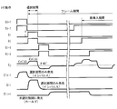
- FIG. 2 is a timing chart showing the operation of the pixel circuit 6 according to the first embodiment.
- the pixel circuit 6 includes an organic EL (Electroluminescence) diode 7 (element), thin film transistors (TFTs) T1 to T3, and a capacitor C, which are elements that emit light with a luminance corresponding to a flowing current.
- the thin film transistors T1 to T3 may be N-channel thin film transistors. Accordingly, an amorphous silicon panel in which a P-channel thin film transistor is difficult to be made can be used for the display device 1.
- the gate of the thin film transistor T1 is connected to the i-th scanning line Gi.
- the gate of the thin film transistor T2 is connected to the i-th scanning line Ri.
- the gate of the thin film transistor T3 is connected to the source of the thin film transistor T2 and one end of the capacitor C.
- the drain of the thin film transistor T3 is connected to the power supply line Vp.
- the source of the thin film transistor T3 is connected to the drain of the thin film transistor T1, the other end of the capacitor C, and the anode of the organic EL diode 7.
- the source of the thin film transistor T1 is connected to the data signal line Sj in the jth column.
- the drain of the thin film transistor T2 and the cathode of the organic EL diode 7 are electrically grounded.
- the data signal line Sj in the j-th column is connected to the low gradation display program current source I1 when the pixel Aij displays a low gradation.
- the data signal line Sj in the j-th column is connected to the program current source I2 for high gradation display. Switching of connection between the data signal line Sj in the j-th column and the current sources I1 and I2 is performed by the switch SW.
- Each of the current sources I1 and I2 and the switch SW is included in the source driver circuit 2 shown in FIG.
- the signal levels of the scanning lines Gi and Ri in the selected row change from L (low) to H (high).
- the signal level changes from H to L after the selection period ends.
- the pixel circuit 6 is driven in the impulse mode when the pixel Aij displays a low gradation, that is, the organic EL diode 7 emits light only during the selection period.
- the program current I is sourced, that is, the j-th column data signal line Sj is connected to the low gradation display program current source I1.
- the potential corresponding to the data of the data signal line Sj is positive, and the potential of the source of the thin film transistor T1 is also positive. Further, during the selection period, the thin film transistors T1 and T2 are turned on. Therefore, the potential of the drain of the thin film transistor T1, the other end of the capacitor C, and the anode of the organic EL diode 7 is positive because the potential of the source of the thin film transistor T1 is written. The potential of the gate of the thin film transistor T3 and one end of the capacitor C becomes the ground potential.
- the organic EL diode 7 since a forward bias voltage is applied to the organic EL diode 7, the organic EL diode 7 is turned on. Further, since the gate-source voltage Vgs of the thin film transistor T3 becomes negative, the thin film transistor T3 is turned off.
- the program current I flows through the output of the low gradation display program current source I1 ⁇ the data signal line Sj ⁇ the source of the thin film transistor T1 ⁇ the drain of the thin film transistor T1 ⁇ the anode of the organic EL diode 7 ⁇ the cathode of the organic EL diode 7.
- the organic EL diode 7 emits light.
- the current waveforms Eli (i row) and Eli-1 (i-1 row) of the organic EL diode 7 rise gently during the passage of the delay time and the rise time.
- the light emission luminance of the organic EL diode 7 is determined by the current value of the program current I set by the low gradation display program current source I1.
- the current value of the program current I and the gradation value are in a proportional relationship.
- the thin film transistors T1 and T2 are turned off and the program current I does not flow. Further, since the gate-source voltage Vgs of the thin film transistor T3 is zero or negative, T3 is also turned off. Therefore, the organic EL diode 7 is turned off.
- the thin film transistor T1 does not turn off immediately even when the signal level of the scanning line Gi changes from H to L, and requires a delay time and a fall time before turning off. For this reason, the current waveforms Eli and Eli-1 of the organic EL diode 7 fall gently during the passage of the delay time and the fall time.
- the delay time refers to the time from the time when an ideal pulse appears until the actual pulse amplitude reaches 10%, or the amplitude ranges from 10% to 0 with respect to the drain current pulse of the thin film transistor. Indicates the time until The rise time indicates the time until the amplitude becomes 10% to 90%. Further, the fall time indicates the time until the amplitude becomes 90% to 10%.
- the current waveform Eli in FIG. 2 is the current waveform of the pixel Aij controlled by the scanning lines Gi and Ri, but not all the pixels controlled by the scanning lines Gi and Ri are driven in the impulse mode. Absent.
- Corresponding to the data signal line Sj there are pixels driven in the impulse mode and pixels driven in the hold mode. Therefore, in order to perform black insertion in pixels driven in some hold modes, a black insertion period is provided with the signal level of the scanning line Gi set to L and the signal level of the scanning line Ri set to H.
- the pixel circuit 6 is driven in the hold mode, that is, the organic EL diode 7 does not emit light during the selection period but continues to emit light after the selection period.
- the program current I ' is sinked, that is, the j-th column data signal line Sj is connected to the high gradation display program current source I2.
- the potential of the data signal line Sj is negative, and the potential of the source of the thin film transistor T1 is also negative. Further, during the selection period, the thin film transistors T1 and T2 are turned on. Therefore, the potential of the drain of the thin film transistor T1, the other end of the capacitor C, and the anode of the organic EL diode 7 is negative because the potential of the source of the thin film transistor T1 is written. Further, the potential of the gate of the thin film transistor T3 and one end of the capacitor C becomes the ground potential.
- the organic EL diode 7 is turned off. Further, since the gate-source voltage Vgs of the thin film transistor T3 is positive, the thin film transistor T3 is turned on.
- the power supply line Vp ⁇ the drain of the thin film transistor T3 ⁇ the source of the thin film transistor T3 ⁇ the drain of the thin film transistor T1 ⁇ the source of the thin film transistor T1 ⁇ the data signal line Sj ⁇ the input of the program current source I2 for high gradation display ⁇ the program current source I2 for high gradation display.
- the program current I ′ flows through the output path.
- the current value of the program current I ' corresponds to the gradation value and is set by the program current source I2 for high gradation display.
- the source potential of the thin film transistor T3 varies according to the anode potential of the organic EL diode 7. Further, the gate potential of the thin film transistor T3 follows the fluctuation of the source potential of the thin film transistor T3 so that the gate-source voltage Vgs of the thin film transistor T3 becomes constant. This is because the thin film transistor T2 is floating because it is turned off.
- the gate-source voltage Vgs of the thin film transistor T3 during the selection period is held even after the selection period ends because the capacitor C is charged during the selection period by the gate-source voltage Vgs. For this reason, after the selection period ends, the thin film transistors T1 and T2 are turned off, but the thin film transistor T3 remains on.
- the program current I ′′ having a current value substantially equal to the program current I ′ in the selection period is the power supply line Vp ⁇ the drain of the thin film transistor T3 ⁇ the source of the thin film transistor T3 ⁇ the anode of the organic EL diode 7 ⁇ the cathode of the organic EL diode 7. It flows along the route.
- the thin film transistor T1 does not turn off immediately even when the signal level of the scanning line Gi changes from H to L, and requires a delay time and a fall time before turning off. For this reason, the current waveform Eli + 1 (i + 1 row) of the organic EL diode 7 falls gently while the delay time and the fall time elapse.
- the signal level of the scanning line Gi is set to L (low), and the signal level of the scanning line Ri is set to H (high).
- the thin film transistor T1 is turned off and the thin film transistor T2 is turned on.
- the thin film transistor T3 is turned off because the gate potential becomes the ground potential when the thin film transistor T2 is turned on. Since the thin film transistor T3 is turned off, the program current I ′′ does not flow, and the organic EL diode 7 is turned off.
- the thin film transistor T3 does not turn off immediately even when the signal level of the scanning line Ri changes from L to H, and requires a delay time and a fall time before turning off. For this reason, the current waveform Eli + 1 of the organic EL diode 7 falls gently while the delay time and the fall time elapse.
- the direction of the program current I flowing through the data signal line Sj in the impulse mode and the direction of the program current I ′ flowing through the data signal line Sj in the hold mode are on the data signal line Sj. They are opposite to each other.
- the data output timing can be made the same as the start and end of the selection period, so that it is not necessary to complicate the circuit for controlling the data output timing.
- the luminance of the EL element is controlled by the current that flows directly to the EL element, it is possible to obtain a uniform luminance distribution that is not affected by variations (individual differences) in driving TFTs used for driving the pixel circuit.
- all gradations are set to 0 to 255, and driving is performed in an impulse mode up to 32 gradations, and after 33 gradations, “90% of one frame period” It is driven in “hold mode with black inserted in period”.
- Black may be driven in either impulse mode or hold mode for 0 gradation.
- the current value at the maximum gradation was 1 mA or more, but it could be 10 ⁇ A. As a result, it has become possible to extend the service life compared to the prior art.
- the current control region can be effectively used. Can do.
- the gradation region driven in the impulse mode is set large, the necessary current value increases and a large current flows instantaneously, which is not preferable.
- the technique described in this embodiment is useful also from the viewpoint of reducing power consumption.
- the hold mode of the conventional drive circuit current is always supplied to the organic EL element through the drive transistor during light emission.
- the driving transistor is driven in a saturation region, a voltage drop is caused by the driving transistor, and the energy becomes heat and is lost without contributing to light emission.
- the impulse mode light emission current is supplied through a switching element operating in a linear region, so that power loss can be minimized. That is, as compared with driving in the hold mode of the conventional driving circuit, power loss can be reduced when driven in the impulse mode, so that a display device with reduced power consumption can be realized.
- the gradation value for displaying white and the gradation value for displaying black are different colors. Becomes larger than the gradation value for displaying. In such a first pattern, the deterioration of display quality is limited with respect to gradation unevenness.
- the pixel circuit can be used only in the hold mode regardless of the gradation. What is necessary is just to drive.
- the distribution of gradation values in the second pattern for displaying content such as photographs and moving images in which gradation unevenness directly leads to deterioration in display quality is, for example, a wide distribution over all gradations.
- the pixel circuit may be driven in both the impulse mode and the hold mode.
- FIG. 4 shows an example of a flowchart in the case where the driving method for driving only in the hold mode and the driving method for driving in both the impulse mode and the hold mode are separated according to the video source. That is, the display device 1 has means for analyzing the video signal, and the two driving methods are switched depending on whether the display is a moving image, whether the area of the black display is large, and whether the display is mainly text.
- step s1 it is first determined in step s1 whether the video signal is a moving image.
- a driving method for driving in both the impulse mode and the hold mode is used.
- step s2 If the video signal is not a moving image (No in step s1), in order to determine the size of the black display area, it is determined whether the intermediate length signal is 90% or more (step s2). When the intermediate length signal is not 90% or more (No in step s2), a driving method for driving only in the hold mode is used.
- step s3 If the intermediate length signal is 90% or more (Yes in step s2), it is determined whether or not it is a text subject (step s3). If the text is the main subject (Yes in step s3), a driving method for driving only in the hold mode is used. If it is not a text subject (No in step s3), a driving method for driving in both the impulse mode and the hold mode is used.
- the two driving methods can be selected only by switching the signal current source, it is possible to change the control each time the video is switched without performing special control.
- the reference for switching between the impulse mode and the hold mode that is, the reference for determining whether the pixel circuit 6 is driven in both the impulse mode and the hold mode or only in the hold mode is determined.
- it may be a distribution of gradation values constituting an image.
- the reference may be included in the source driver circuit 2 or the control circuit 5.
- Example 2 The following will describe another embodiment of the present invention with reference to FIGS.
- the configuration other than that described in the second embodiment is the same as that of the first embodiment.
- members having the same functions as those shown in the drawings of the first embodiment are given the same reference numerals, and explanation thereof is omitted.
- FIG. 5 is a circuit diagram of the pixel circuit 8 according to the second embodiment.
- the pixel circuit 8 differs from the pixel circuit 6 according to the first embodiment in the following points.
- the drain of the thin film transistor T2 is electrically grounded, and the drain of the thin film transistor T3 is connected to the power supply line Vp.
- the drain of the thin film transistor T2 and the drain of the thin film transistor T3 are connected to the common power supply line Pi.
- the potential of the common power supply line Pi is set to the ground potential during the selection period, and is set to the potential Vp ′ higher than the ground potential during the non-selection period.
- the pixel circuit 8 not only can perform the same operation as the pixel circuit 6 according to the first embodiment, but also connects the power line with the ground potential and the power line with the potential Vp ′ larger than the ground potential to the common power line Pi. Can be made common. Therefore, one power supply line can be reduced per row.
- Example 3 The following will describe still another embodiment of the present invention with reference to FIGS.
- the configurations other than those described in the third embodiment are the same as those in the first and second embodiments.
- members having the same functions as those shown in the drawings of the first and second embodiments are given the same reference numerals, and explanation thereof is omitted.
- FIG. 7 is a circuit diagram of the pixel circuit 9 according to the third embodiment.
- the pixel circuit 8 differs from the pixel circuit 6 according to the first embodiment in the following points.
- the gate of the thin film transistor T1 is connected to the i-th scanning line Gi, and the gate of the thin film transistor T2 is connected to the i-th scanning line Ri.
- the gate of the thin film transistor T1 and the gate of the thin film transistor T2 are both connected to the i-th scanning line Gi.
- the pixel circuit 9 not only enables an operation without black insertion in the pixel circuit 6 according to the first embodiment, but also allows the scanning line Gi to be shared, thereby reducing the number of scanning lines by one per row. Is possible.
- FIG. 8 is a timing chart illustrating the operation of the pixel circuit 9 according to the third embodiment. Unlike the timing chart of FIG. 3, the waveform of the scanning line Ri is not included.
- the pixel circuits 6, 8, and 9 of the present embodiment can be applied not only to the organic EL diode 7 but also to a semiconductor light emitting diode.
- the low gradation display program current source I 1 and the high gradation display program current source I 2 may be current sources whose output directions are opposite to each other.
- the sign of the slope of the voltage change with respect to the gradation change is positive, and the other is negative.
- a voltage source may be used.
- the impulse mode is the low gradation.
- the hold mode may be driven on the high gradation side.
- the low gradation side is more than the 1 ⁇ 2 luminance from the lowest gradation. It is a range up to a small gradation, and the high gradation side may be a range from a gradation smaller than the 1/2 luminance to a maximum gradation.
- the color reproduction range is widened on both the low gradation side and the high gradation side by the combination of the impulse mode and the hold mode. Therefore, the entire color reproduction range by the combination of each color is greatly expanded.
- the plurality of scanning lines include scanning lines G 1, G 2,..., Gn, Gi and scanning lines R 1, R 2,.
- the thin film transistor T1 includes a thin film transistor T2, a thin film transistor T3, and a capacitor C.
- the thin film transistor T1 has a gate connected to the scan line Gi, a source connected to the data signal line Sj, and the thin film transistor T2 has a gate connected to the scan line Ri and a drain connected to the data line Sj.
- the source is connected to the gate of the thin film transistor T3 and one end of the capacitor C, the drain of the thin film transistor T3 is connected to the power supply line Vp, the source is the drain of the thin film transistor T1, the other end of the capacitor C, and the organic EL Connected to the anode of the diode 7, the cathode of the organic EL diode 7 is electrically grounded, and the source
- the driver circuit 3 includes a low gradation display program current source I1, a high gradation display program current source I2, and a switch SW.
- the switch SW includes pixels A11,..., A1m,.
- the data signal lines S1, S2,..., Sm, Sj are connected to the low gradation display program current source I1, and the pixels A11,. .., when A1m,..., An1,..., Anm, Aij display the image in the hold mode, the data signal lines S1, S2,. It may be connected to the program current source I2.
- the signal level of the scanning line Gi and the signal level of the scanning line Ri are set to the high level.
- programming is performed in the path of the low gradation display program current source I 1 ⁇ the data signal line Sj ⁇ the source of the thin film transistor T 1 ⁇ the drain of the thin film transistor T 1 ⁇ the anode of the organic EL diode 7 ⁇ the cathode of the organic EL diode 7.
- the current I is supplied, and the organic EL diode 7 emits light.
- the organic EL diode 7 is turned off. Further, since the gate-source voltage of the thin film transistor T3 is positive, the thin film transistor T3 is turned on.
- the program current I ′ is supplied through the path of the power line Vp ⁇ the drain of the thin film transistor T3 ⁇ the source of the thin film transistor T3 ⁇ the drain of the thin film transistor T1 ⁇ the source of the thin film transistor T1 ⁇ the data signal line Sj ⁇ the program current source I2 for high gradation display.
- the gate-source voltage of the thin film transistor T3 during the selection period is maintained even after the selection period ends because the capacitor C is charged during the selection period by the gate-source voltage. For this reason, after the selection period ends, the thin film transistor T1 and the thin film transistor T2 are turned off, but the thin film transistor T3 remains on.
- the program current I ′′ whose current value is substantially equal to the program current I ′ is supplied through the path of the power supply line Vp ⁇ the drain of the thin film transistor T3 ⁇ the source of the thin film transistor T3 ⁇ the anode of the organic EL diode 7 ⁇ the cathode of the organic EL diode 7. Is done.
- the signal level of the scanning line Gi is set to low and the signal level of the scanning line Ri is set to high.
- the thin film transistor T1 is turned off and the thin film transistor T2 is turned on.
- the thin film transistor T3 is turned off because the gate potential becomes the ground potential when the thin film transistor T2 is turned on. Since the thin film transistor T3 is turned off, the program current I ′′ is not supplied and the organic EL diode 7 is turned off.
- the plurality of scanning lines include scanning lines G1, G2,..., Gn, Gi and scanning lines R1, R2,..., Rn, Ri
- the pixel circuit 8 includes the thin film transistors T1
- the thin film transistor T1 includes a thin film transistor T2, a thin film transistor T3, and a capacitor C.
- the thin film transistor T1 has a gate connected to the scan line Gi, a source connected to the data signal line Sj
- the thin film transistor T2 has a gate connected to the scan line Ri and a drain connected to the data line Sj.
- the common power supply line Pi is grounded, the source is connected to the gate of the thin film transistor T3 and one end of the capacitor C, the drain of the thin film transistor T3 is connected to the common power supply line Pi, the source is the drain of the thin film transistor T1, and the other end of the capacitor C
- the cathode of the organic EL diode 7 is electrically connected to the anode of the organic EL diode 7.
- the source driver circuit 3 includes a low gradation display program current source I1, a high gradation display program current source I2, and a switch SW.
- the switch SW includes pixels A11,..., A1m,.
- the data signal lines S1, S2,..., Sm, Sj are connected to the low gradation display program current source I1, and the pixels
- A11,..., A1m,..., An1,..., Anm, Aij display the image in the hold mode, the data signal lines S1, S2,.
- the potential of the common power supply line Pi connected to the gradation display program current source I2 may be a ground potential during the selection period and may be higher than the ground potential during the non-selection period.
- the pixel circuit 8 not only enables the same operation as the pixel circuit 6 in which the drain of the thin film transistor T3 is connected to the power supply line Vp, but also the power supply line having the ground potential and the power supply having the potential Vp ′ larger than the ground potential. And a common power line Pi. Therefore, one power supply line can be reduced per row.
- the pixel circuit 9 includes a thin film transistor T1, a thin film transistor T2, a thin film transistor T3, and a capacitor C.
- the thin film transistor T1 has a gate connected to the scanning line Gi, a source connected to the data signal line Sj, and a thin film transistor T2.
- the gate is connected to the scanning line Gi, the drain is electrically grounded, the source is connected to the gate of the thin film transistor T3 and one end of the capacitor C, the thin film transistor T3 has the drain connected to the power supply line Vp, and the source is The drain of the thin film transistor T1, the other end of the capacitor C and the anode of the organic EL diode 7 are connected, the cathode of the organic EL diode 7 is electrically grounded, and the source driver circuit 3 Has program current source I2 and switch SW for high gradation display , A1m,..., An1,..., Ann, Aij, when the image is displayed in the impulse mode, the data signal lines S1, S2,.
- the gate of the thin film transistor T1 and the gate of the thin film transistor T2 are both connected to the scanning line Gi.
- the pixel circuit 9 not only allows the pixel circuits 6 and 8 using the scanning line Gi and the scanning line Ri not to perform black insertion, but also allows the scanning line Gi to be shared. It is possible to reduce one per hit.
- the program current source for low gradation display I1 and the program current source for high gradation display I2 may be current sources whose output directions are opposite to each other.
- the direction of the current flowing through Sj (the second current) is opposite to each other on the data signal lines S1, S2,... Sm, Sj, and the impulse mode and the hold mode can be distinguished. It becomes possible. Therefore, even in the impulse mode, light emission can be continued until the selection period ends.
- the data output timing can be made the same as the start and end of the selection period, so that it is not necessary to complicate the circuit for controlling the data output timing.
- the luminance of the element is controlled by the current that directly flows through the organic EL diode 7, a uniform luminance distribution that is not affected by variations (individual differences) in driving TFTs used for driving the pixel circuit can be obtained.
- the low gradation display program current source I1 and the high gradation display program current source I2 are voltage sources in which the sign of the slope of the voltage change with respect to the gradation change is positive and the other is negative. There may be.
- the thin film transistor T1, the thin film transistor T2, and the thin film transistor T3 may be N-channel thin film transistors.
- an amorphous silicon panel in which a P-channel thin film transistor is difficult to make can be used for the display device 1.
- the impulse mode is driven on the low gradation side, and the hold mode is the high order. It may be driven on the adjustment side.
- the impulse mode is the low gradation side.
- the hold mode may be driven on the high gradation side.
- the low gradation side has the lowest gradation.
- the high gradation side may be a range from the gradation smaller than the half luminance to the highest gradation.
- the low gradation side is The range may be from the lowest gradation to a gradation smaller than the 1/2 luminance, and the high gradation side may be a range from the gradation smaller than the 1/2 luminance to the highest gradation.
- the source driver circuit 3 has a reference for determining whether to drive the pixel circuit 6 in both the impulse mode and the hold mode, or to drive the pixel circuit 6 only in the hold mode.
- the reference may be a distribution of gradation values forming the image.
- the gradation value for displaying white and the gradation value for displaying black are different colors. Becomes larger than the gradation value for displaying. In such a first pattern, the deterioration of display quality is limited with respect to gradation unevenness. Therefore, if the pixel circuit 6 is driven only in the hold mode regardless of the gradation with emphasis on power, the display quality is limited. Good.
- the distribution of gradation values in the second pattern for displaying content such as photographs and moving images in which gradation unevenness directly leads to deterioration in display quality is, for example, a wide distribution over all gradations.
- the pixel circuit 6 may be driven in both the impulse mode and the hold mode.
- the present invention can perform gradation control more easily than before, can achieve a longer life due to a decrease in instantaneous luminance, and can improve moving image performance, it is suitable for a display device that displays full-color images. Can be used.
Landscapes
- Engineering & Computer Science (AREA)
- Physics & Mathematics (AREA)
- Computer Hardware Design (AREA)
- General Physics & Mathematics (AREA)
- Theoretical Computer Science (AREA)
- Control Of Indicators Other Than Cathode Ray Tubes (AREA)
- Control Of El Displays (AREA)
- Electroluminescent Light Sources (AREA)
Abstract
Description
図3は、本実施形態に係る表示装置1の構成を示すブロック図である。表示装置1は、複数本(m本)のデータ信号線S1,S2,・・・,Smを駆動するソースドライバ回路2と、複数本(n本)の走査線G1,G2,・・・,Gn及び複数本(n本)の走査線R1,R2,・・・、Rnを制御するゲートドライバ回路3と、m×n個の画素A11,・・・,A1m,・・・,An1,・・・,Anmを備える表示部4と、ソースドライバ回路2及びゲートドライバ回路3を制御するためのコントロール回路5とを備えている。
図1は、本実施例1に係る画素回路6の回路図であり、図2は、本実施例1に係る画素回路6の動作を示すタイミングチャートである。まずは画素回路6の構成について図1を参照して説明する。

本発明の他の実施例について図5及び図6に基づいて説明すれば、以下の通りである。なお、本実施例2において説明すること以外の構成は、前記実施例1と同じである。また、説明の便宜上、前記実施例1の図面に示した部材と同一の機能を有する部材については、同一の符号を付し、その説明を省略する。
本発明のさらに別の実施例について図7及び図8に基づいて説明すれば、以下の通りである。なお、本実施例3において説明すること以外の構成は、前記実施例1,2と同じである。また、説明の便宜上、前記実施例1,2の図面に示した部材と同一の機能を有する部材については、同一の符号を付し、その説明を省略する。
表示装置1では、複数の上記走査線は、走査線G1,G2,・・・,Gn、Gi及び走査線R1,R2,・・・,Rn,Riからなり、画素回路6は、薄膜トランジスタT1、薄膜トランジスタT2、薄膜トランジスタT3及び容量Cを有し、薄膜トランジスタT1は、ゲートが走査線Giに接続され、ソースがデータ信号線Sjに接続され、薄膜トランジスタT2は、ゲートが走査線Riに接続され、ドレインが電気的に接地され、ソースが薄膜トランジスタT3のゲート及び容量Cの一端に接続され、薄膜トランジスタT3は、ドレインが電源線Vpに接続され、ソースが、薄膜トランジスタT1のドレイン、容量Cの他端及び有機ELダイオード7のアノードに接続され、有機ELダイオード7のカソードが電気的に接地され、ソースドライバ回路3は、低階調表示用プログラム電流源I1、高階調表示用プログラム電流源I2及びスイッチSWを有し、スイッチSWは、画素A11,・・・,A1m,・・・,An1,・・・,Anm、Aijが上記インパルスモードにより画像を表示する場合は、データ信号線S1,S2,・・・,Sm、Sjを低階調表示用プログラム電流源I1に接続し、画素A11,・・・,A1m,・・・,An1,・・・,Anm、Aijが上記ホールドモードにより上記画像を表示する場合は、データ信号線S1,S2,・・・,Sm、Sjを高階調表示用プログラム電流源I2に接続してもよい。
2 ソースドライバ回路
3 ゲートドライバ回路
4 表示部
5 コントロール回路
6,8,9 画素回路
7 有機ELダイオード(素子、有機エレクトロルミネッセンスダイオード)
A11,・・・,A1m,・・・,An1,・・・,Anm、Aij 画素
C 容量
G1,G2,・・・,Gn、Gi 走査線(第1走査線)
R1,R2,・・・,Rn,Ri 走査線(第2走査線)
I プログラム電流(発光信号)
I’ プログラム電流(発光信号)
I’’ プログラム電流(発光信号)
I1 低階調表示用プログラム電流源(第1の信号源)
I2 高階調表示用プログラム電流源(第2の信号源)
Pi 共通電源線
s1~s3 ステップ
S1,S2,・・・,Sm、Sj データ信号線
SW スイッチ(スイッチ手段)
T1 薄膜トランジスタ(第1薄膜トランジスタ)
T2 薄膜トランジスタ(第2薄膜トランジスタ)
T3 薄膜トランジスタ(第3薄膜トランジスタ)
Vgs ゲート-ソース間電圧
Vp 電源線
Vp’ 接地電位よりも大きい電位
Claims (15)
- 一方向に伸びる複数の走査線と、他方向に伸びる複数のデータ信号線と、複数の上記データ信号線を駆動するソースドライバ回路と、複数の上記走査線を制御するゲートドライバ回路と、上記走査線および上記データ信号線の交差部に対応して設けられる複数の画素とを備え、流れる電流に応じた輝度で発光する素子を上記画素が有し、上記ゲートドライバ回路が上記走査線を選択する期間を選択期間と称する表示装置であって、
上記画素の画素回路は、上記素子が上記選択期間のみ発光するインパルスモードで駆動されるか、上記素子が上記選択期間中は発光せず上記選択期間後に発光を続けるホールドモードで駆動されると共に、
上記画素回路は、上記インパルスモードで駆動される際に発光信号を供給する第1の信号源と、上記ホールドモードで駆動される際に発光信号を供給する第2の信号源とを有することを特徴とする表示装置。 - 複数の上記走査線は、複数の第1走査線及び複数の第2走査線からなり、
上記画素回路は、第1薄膜トランジスタ、第2薄膜トランジスタ、第3薄膜トランジスタ及び容量を有し、
上記第1薄膜トランジスタは、ゲートが上記第1走査線に接続され、ソースが上記データ信号線に接続され、
上記第2薄膜トランジスタは、ゲートが上記第2走査線に接続され、ドレインが電気的に接地され、ソースが上記第3薄膜トランジスタのゲート及び上記容量の一端に接続され、
上記第3薄膜トランジスタは、ドレインが電源線に接続され、ソースが、上記第1薄膜トランジスタのドレイン、上記容量の他端及び上記素子のアノードに接続され、
上記素子のカソードが電気的に接地され、
上記ソースドライバ回路は、上記第1の信号源、上記第2の信号源及びスイッチ手段を有し、
上記スイッチ手段は、上記画素が上記インパルスモードにより画像を表示する場合は、上記データ信号線を上記第1の信号源に接続し、上記画素が上記ホールドモードにより上記画像を表示する場合は、上記データ信号線を上記第2の信号源に接続することを特徴とする請求項1に記載の表示装置。 - 複数の上記走査線は、複数の第1走査線及び複数の第2走査線からなり、
上記画素回路は、第1薄膜トランジスタ、第2薄膜トランジスタ、第3薄膜トランジスタ及び容量を有し、
上記第1薄膜トランジスタは、ゲートが上記第1走査線に接続され、ソースが上記データ信号線に接続され、
上記第2薄膜トランジスタは、ゲートが上記第2走査線に接続され、ドレインが共通電源線に接地され、ソースが上記第3薄膜トランジスタのゲート及び上記容量の一端に接続され、
上記第3薄膜トランジスタは、ドレインが上記共通電源線に接続され、ソースが、上記第1薄膜トランジスタのドレイン、上記容量の他端及び上記素子のアノードに接続され、
上記素子のカソードが電気的に接地され、
上記ソースドライバ回路は、上記第1の信号源、上記第2の信号源及びスイッチ手段を有し、
上記スイッチ手段は、上記画素が上記インパルスモードにより画像を表示する場合は、上記データ信号線を上記第1の信号源に接続し、上記画素が上記ホールドモードにより上記画像を表示する場合は、上記データ信号線を上記第2の信号源に接続し、
上記共通電源線の電位は、上記選択期間中は接地電位とし、非選択期間中は接地電位よりも大きい電位とすることを特徴とする請求項1に記載の表示装置。 - 上記画素回路は、第1薄膜トランジスタ、第2薄膜トランジスタ、第3薄膜トランジスタ及び容量を有し、
上記第1薄膜トランジスタは、ゲートが上記走査線に接続され、ソースが上記データ信号線に接続され、
上記第2薄膜トランジスタは、ゲートが上記走査線に接続され、ドレインが電気的に接地され、ソースが上記第3薄膜トランジスタのゲート及び上記容量の一端に接続され、
上記第3薄膜トランジスタは、ドレインが電源線に接続され、ソースが、上記第1薄膜トランジスタのドレイン、上記容量の他端及び上記素子のアノードに接続され、
上記素子のカソードが電気的に接地され、
上記ソースドライバ回路は、上記第1の信号源、上記第2の信号源及びスイッチ手段を有し、
上記スイッチ手段は、上記画素が上記インパルスモードにより画像を表示する場合は、上記データ信号線を上記第1の信号源に接続し、上記画素が上記ホールドモードにより上記画像を表示する場合は、上記データ信号線を上記第2の信号源に接続することを特徴とする請求項1に記載の表示装置。 - 上記第1の信号源および上記第2の信号源は、出力する電流の向きが互いに逆の電流源であることを特徴とする請求項1に記載の表示装置。
- 上記第1の信号源および上記第2の信号源は、階調変化に対する電圧変化の傾きの符号が、一方が正であり他方が負である電圧源であることを特徴とする請求項1に記載の表示装置。
- 上記第1薄膜トランジスタ、上記第2薄膜トランジスタ及び上記第3薄膜トランジスタは、Nチャネルの薄膜トランジスタであることを特徴とする請求項2に記載の表示装置。
- 上記発光信号の全階調を、それぞれ低階調側と高階調側とに分けたとき、上記インパルスモードは上記低階調側で駆動され、上記ホールドモードは上記高階調側で駆動されることを特徴とする請求項1に記載の表示装置。
- 上記発光信号の全階調に関して、該全階調の半分の輝度を1/2輝度としたとき、上記低階調側は、最低階調から上記1/2輝度より小さい階調までの範囲であり、上記高階調側は、上記1/2輝度より小さい階調から最高階調までの範囲であることを特徴とする請求項8に記載の表示装置。
- 上記ソースドライバ回路は、上記インパルスモードと上記ホールドモードとの両方で上記画素回路を駆動するか、上記ホールドモードのみで上記画素回路を駆動するかを決定する基準を有しており、
上記基準は、上記画像を構成する階調値の分布であることを特徴とする請求項2に記載の表示装置。 - 上記素子は、有機エレクトロルミネッセンスダイオードであることを特徴とする請求項1に記載の表示装置。
- 一方向に伸びる複数の走査線と、他方向に伸びる複数のデータ信号線と、複数の上記データ信号線を駆動するソースドライバ回路と、複数の上記走査線を制御するゲートドライバ回路と、上記走査線および上記データ信号線の交差部に対応して設けられる複数の画素とを備え、流れる電流に応じた輝度で発光する素子を上記画素が有し、上記ゲートドライバ回路が上記走査線を選択する期間を選択期間と称する表示装置の駆動方法であって、
上記素子が上記選択期間のみ発光するインパルスモードで上記画素の画素回路を駆動する工程と、
上記素子が上記選択期間中は発光せず上記選択期間後に発光を続けるホールドモードで上記画素回路を駆動する工程と、
上記画素回路が上記インパルスモードで駆動される場合に、第1の信号源により発光信号を供給する工程と、
上記画素回路が上記ホールドモードで駆動される場合に、第2の信号源により発光信号を供給する工程とを含むことを特徴とする表示装置の駆動方法。 - 上記発光信号の全階調を、それぞれ低階調側と高階調側とに分けたとき、上記インパルスモードは上記低階調側で駆動され、上記ホールドモードは上記高階調側で駆動されることを特徴とする請求項12に記載の表示装置の駆動方法。
- 上記発光信号の全階調に関して、該全階調の半分の輝度を1/2輝度としたとき、上記低階調側は、最低階調から上記1/2輝度より小さい階調までの範囲であり、上記高階調側は、上記1/2輝度より小さい階調から最高階調までの範囲であることを特徴とする請求項13に記載の表示装置の駆動方法。
- 上記素子は、有機エレクトロルミネッセンスダイオードであることを特徴とする請求項12に記載の表示装置の駆動方法。
Priority Applications (7)
| Application Number | Priority Date | Filing Date | Title |
|---|---|---|---|
| RU2011150902/08A RU2521266C2 (ru) | 2009-06-04 | 2010-03-04 | Дисплейное устройство и способ управления дисплейным устройством |
| US13/375,769 US8610749B2 (en) | 2009-06-04 | 2010-03-04 | Display device and drive method for display device |
| BRPI1010033-4A BRPI1010033A2 (pt) | 2009-06-04 | 2010-03-04 | dispositivo de exibição e método de acionamento para dispositivo de exibição |
| EP10783073.9A EP2439724B1 (en) | 2009-06-04 | 2010-03-04 | Display device and drive method for display device |
| CN201080024411.4A CN102804246B (zh) | 2009-06-04 | 2010-03-04 | 显示装置和显示装置的驱动方法 |
| JP2011518215A JP5280534B2 (ja) | 2009-06-04 | 2010-03-04 | 表示装置及び表示装置の駆動方法 |
| KR1020117031248A KR101372760B1 (ko) | 2009-06-04 | 2010-03-04 | 표시 장치 및 표시 장치의 구동 방법 |
Applications Claiming Priority (2)
| Application Number | Priority Date | Filing Date | Title |
|---|---|---|---|
| JP2009135286 | 2009-06-04 | ||
| JP2009-135286 | 2009-06-04 |
Publications (1)
| Publication Number | Publication Date |
|---|---|
| WO2010140285A1 true WO2010140285A1 (ja) | 2010-12-09 |
Family
ID=43297428
Family Applications (1)
| Application Number | Title | Priority Date | Filing Date |
|---|---|---|---|
| PCT/JP2010/001523 Ceased WO2010140285A1 (ja) | 2009-06-04 | 2010-03-04 | 表示装置及び表示装置の駆動方法 |
Country Status (8)
| Country | Link |
|---|---|
| US (1) | US8610749B2 (ja) |
| EP (1) | EP2439724B1 (ja) |
| JP (1) | JP5280534B2 (ja) |
| KR (1) | KR101372760B1 (ja) |
| CN (1) | CN102804246B (ja) |
| BR (1) | BRPI1010033A2 (ja) |
| RU (1) | RU2521266C2 (ja) |
| WO (1) | WO2010140285A1 (ja) |
Cited By (5)
| Publication number | Priority date | Publication date | Assignee | Title |
|---|---|---|---|---|
| JP2018013766A (ja) * | 2016-07-22 | 2018-01-25 | 三星ディスプレイ株式會社Samsung Display Co.,Ltd. | 表示装置及びその駆動方法 |
| US10242617B2 (en) | 2016-06-03 | 2019-03-26 | Semiconductor Energy Laboratory Co., Ltd. | Display device, display module, electronic device, and driving method |
| US10403204B2 (en) | 2016-07-12 | 2019-09-03 | Semiconductor Energy Laboratory Co., Ltd. | Display device, display module, electronic device, and method for driving display device |
| CN110930947A (zh) * | 2019-11-28 | 2020-03-27 | 武汉华星光电半导体显示技术有限公司 | 像素补偿电路及其驱动方法、显示装置 |
| WO2021171921A1 (ja) * | 2020-02-27 | 2021-09-02 | 京セラ株式会社 | 表示装置 |
Families Citing this family (8)
| Publication number | Priority date | Publication date | Assignee | Title |
|---|---|---|---|---|
| KR101992405B1 (ko) * | 2012-12-13 | 2019-06-25 | 삼성디스플레이 주식회사 | 화소 및 이를 이용한 유기전계발광 표시장치 |
| KR101676259B1 (ko) * | 2014-10-01 | 2016-11-16 | 엘지디스플레이 주식회사 | 유기 발광 표시 장치 |
| KR102552936B1 (ko) * | 2016-04-12 | 2023-07-10 | 삼성디스플레이 주식회사 | 표시 장치 및 이의 구동 방법 |
| KR102316567B1 (ko) * | 2017-09-29 | 2021-10-25 | 엘지디스플레이 주식회사 | 전계발광 표시장치 및 그 구동방법 |
| JPWO2019124254A1 (ja) * | 2017-12-19 | 2021-01-14 | ソニー株式会社 | 信号処理装置、信号処理方法、及び表示装置 |
| CN108877675B (zh) * | 2018-07-31 | 2020-08-28 | 京东方科技集团股份有限公司 | 一种像素电路、显示面板及其驱动方法、显示装置 |
| JP7362742B2 (ja) * | 2019-07-31 | 2023-10-17 | 京セラ株式会社 | 表示装置 |
| US12307947B2 (en) * | 2022-10-24 | 2025-05-20 | Dynascan Technology Corp. | Display apparatus including LED array |
Citations (6)
| Publication number | Priority date | Publication date | Assignee | Title |
|---|---|---|---|---|
| JP2001060076A (ja) * | 1999-06-17 | 2001-03-06 | Sony Corp | 画像表示装置 |
| JP2003195810A (ja) | 2001-12-28 | 2003-07-09 | Casio Comput Co Ltd | 駆動回路、駆動装置及び光学要素の駆動方法 |
| JP2004317677A (ja) * | 2003-04-14 | 2004-11-11 | Seiko Epson Corp | 電子回路の駆動方法、電子回路、電気光学装置の駆動方法、電気光学装置及び電子機器 |
| JP2004361935A (ja) * | 2003-05-09 | 2004-12-24 | Semiconductor Energy Lab Co Ltd | 半導体装置およびその駆動方法 |
| JP2007248800A (ja) * | 2006-03-16 | 2007-09-27 | Casio Comput Co Ltd | 表示装置及びその駆動制御方法 |
| JP2009009049A (ja) * | 2007-06-29 | 2009-01-15 | Canon Inc | アクティブマトリクス型有機elディスプレイ及びその階調制御方法 |
Family Cites Families (10)
| Publication number | Priority date | Publication date | Assignee | Title |
|---|---|---|---|---|
| US5426447A (en) * | 1992-11-04 | 1995-06-20 | Yuen Foong Yu H.K. Co., Ltd. | Data driving circuit for LCD display |
| JP4218249B2 (ja) * | 2002-03-07 | 2009-02-04 | 株式会社日立製作所 | 表示装置 |
| CN1666242A (zh) * | 2002-04-26 | 2005-09-07 | 东芝松下显示技术有限公司 | 用于场致发光显示屏的驱动电路 |
| JP3707484B2 (ja) * | 2002-11-27 | 2005-10-19 | セイコーエプソン株式会社 | 電気光学装置、電気光学装置の駆動方法および電子機器 |
| KR100717229B1 (ko) | 2003-02-03 | 2007-05-11 | 샤프 가부시키가이샤 | 액정 표시 장치 |
| US7453427B2 (en) | 2003-05-09 | 2008-11-18 | Semiconductor Energy Laboratory Co., Ltd. | Semiconductor device and driving method thereof |
| JP2004361570A (ja) * | 2003-06-03 | 2004-12-24 | Seiko Epson Corp | 電気光学装置および電子機器 |
| JP4265515B2 (ja) * | 2004-09-29 | 2009-05-20 | カシオ計算機株式会社 | ディスプレイパネル |
| EP1889249B1 (en) | 2005-05-24 | 2013-05-22 | Casio Computer Co., Ltd. | Display apparatus and drive control method thereof |
| US20100309096A1 (en) * | 2007-12-11 | 2010-12-09 | Ippei Inoh | Display device and its display method |
-
2010
- 2010-03-04 RU RU2011150902/08A patent/RU2521266C2/ru active
- 2010-03-04 JP JP2011518215A patent/JP5280534B2/ja not_active Expired - Fee Related
- 2010-03-04 KR KR1020117031248A patent/KR101372760B1/ko not_active Expired - Fee Related
- 2010-03-04 CN CN201080024411.4A patent/CN102804246B/zh not_active Expired - Fee Related
- 2010-03-04 US US13/375,769 patent/US8610749B2/en active Active
- 2010-03-04 WO PCT/JP2010/001523 patent/WO2010140285A1/ja not_active Ceased
- 2010-03-04 BR BRPI1010033-4A patent/BRPI1010033A2/pt not_active Application Discontinuation
- 2010-03-04 EP EP10783073.9A patent/EP2439724B1/en not_active Not-in-force
Patent Citations (6)
| Publication number | Priority date | Publication date | Assignee | Title |
|---|---|---|---|---|
| JP2001060076A (ja) * | 1999-06-17 | 2001-03-06 | Sony Corp | 画像表示装置 |
| JP2003195810A (ja) | 2001-12-28 | 2003-07-09 | Casio Comput Co Ltd | 駆動回路、駆動装置及び光学要素の駆動方法 |
| JP2004317677A (ja) * | 2003-04-14 | 2004-11-11 | Seiko Epson Corp | 電子回路の駆動方法、電子回路、電気光学装置の駆動方法、電気光学装置及び電子機器 |
| JP2004361935A (ja) * | 2003-05-09 | 2004-12-24 | Semiconductor Energy Lab Co Ltd | 半導体装置およびその駆動方法 |
| JP2007248800A (ja) * | 2006-03-16 | 2007-09-27 | Casio Comput Co Ltd | 表示装置及びその駆動制御方法 |
| JP2009009049A (ja) * | 2007-06-29 | 2009-01-15 | Canon Inc | アクティブマトリクス型有機elディスプレイ及びその階調制御方法 |
Non-Patent Citations (1)
| Title |
|---|
| See also references of EP2439724A4 |
Cited By (8)
| Publication number | Priority date | Publication date | Assignee | Title |
|---|---|---|---|---|
| US10242617B2 (en) | 2016-06-03 | 2019-03-26 | Semiconductor Energy Laboratory Co., Ltd. | Display device, display module, electronic device, and driving method |
| US10403204B2 (en) | 2016-07-12 | 2019-09-03 | Semiconductor Energy Laboratory Co., Ltd. | Display device, display module, electronic device, and method for driving display device |
| JP2018013766A (ja) * | 2016-07-22 | 2018-01-25 | 三星ディスプレイ株式會社Samsung Display Co.,Ltd. | 表示装置及びその駆動方法 |
| JP7017315B2 (ja) | 2016-07-22 | 2022-02-08 | 三星ディスプレイ株式會社 | 表示装置 |
| CN110930947A (zh) * | 2019-11-28 | 2020-03-27 | 武汉华星光电半导体显示技术有限公司 | 像素补偿电路及其驱动方法、显示装置 |
| WO2021171921A1 (ja) * | 2020-02-27 | 2021-09-02 | 京セラ株式会社 | 表示装置 |
| JPWO2021171921A1 (ja) * | 2020-02-27 | 2021-09-02 | ||
| JP7362889B2 (ja) | 2020-02-27 | 2023-10-17 | 京セラ株式会社 | 表示装置 |
Also Published As
| Publication number | Publication date |
|---|---|
| US20120075361A1 (en) | 2012-03-29 |
| CN102804246B (zh) | 2014-12-17 |
| US8610749B2 (en) | 2013-12-17 |
| JP5280534B2 (ja) | 2013-09-04 |
| KR101372760B1 (ko) | 2014-03-10 |
| CN102804246A (zh) | 2012-11-28 |
| RU2521266C2 (ru) | 2014-06-27 |
| KR20120017084A (ko) | 2012-02-27 |
| RU2011150902A (ru) | 2013-07-20 |
| BRPI1010033A2 (pt) | 2020-08-25 |
| JPWO2010140285A1 (ja) | 2012-11-15 |
| EP2439724A1 (en) | 2012-04-11 |
| EP2439724B1 (en) | 2016-07-13 |
| EP2439724A4 (en) | 2012-12-26 |
Similar Documents
| Publication | Publication Date | Title |
|---|---|---|
| JP5280534B2 (ja) | 表示装置及び表示装置の駆動方法 | |
| JP4111185B2 (ja) | 電気光学装置、その駆動方法及び電子機器 | |
| JP4915195B2 (ja) | 表示装置 | |
| TWI537922B (zh) | Display device | |
| JP2002351400A (ja) | アクティブマトリクス型表示装置およびアクティブマトリクス型有機エレクトロルミネッセンス表示装置、並びにそれらの駆動方法 | |
| JP4300491B2 (ja) | ディスプレイ装置 | |
| JP4300492B2 (ja) | ディスプレイ装置 | |
| KR20110139764A (ko) | 커패시터 결합된 발광 컨트롤 트랜지스터를 이용한 디스플레이 디바이스 | |
| JP5726325B2 (ja) | 表示装置およびその駆動方法 | |
| CN101520984A (zh) | 场致发光显示面板、集成电路、电子设备和驱动控制方法 | |
| TW200409071A (en) | Electroluminescent display apparatus and driving method thereof | |
| JP4314638B2 (ja) | 表示装置及びその駆動制御方法 | |
| WO2019186865A1 (ja) | 表示装置およびその駆動方法 | |
| JP2006038968A (ja) | 表示装置及びその駆動方法 | |
| JP5545804B2 (ja) | 表示装置 | |
| US20110084992A1 (en) | Active matrix display apparatus | |
| JP4281019B2 (ja) | ディスプレイ装置 | |
| US7285797B2 (en) | Image display apparatus without occurence of nonuniform display | |
| CN101714332B (zh) | 显示器装置和显示器驱动方法 | |
| JP2023039901A (ja) | 表示装置及びその制御方法 | |
| JP4687026B2 (ja) | 表示装置および表示装置の駆動方法 | |
| KR101348406B1 (ko) | 구동회로 및 이를 포함하는 유기 이엘 디스플레이 장치 | |
| JP2011191620A (ja) | 表示装置、表示駆動方法 | |
| KR20090087796A (ko) | 능동 유기 발광 다이오드 디스플레이 | |
| JP2008203387A (ja) | ディスプレイ装置 |
Legal Events
| Date | Code | Title | Description |
|---|---|---|---|
| WWE | Wipo information: entry into national phase |
Ref document number: 201080024411.4 Country of ref document: CN |
|
| 121 | Ep: the epo has been informed by wipo that ep was designated in this application |
Ref document number: 10783073 Country of ref document: EP Kind code of ref document: A1 |
|
| WWE | Wipo information: entry into national phase |
Ref document number: 2011518215 Country of ref document: JP |
|
| WWE | Wipo information: entry into national phase |
Ref document number: 13375769 Country of ref document: US |
|
| NENP | Non-entry into the national phase |
Ref country code: DE |
|
| REEP | Request for entry into the european phase |
Ref document number: 2010783073 Country of ref document: EP |
|
| WWE | Wipo information: entry into national phase |
Ref document number: 2010783073 Country of ref document: EP |
|
| WWE | Wipo information: entry into national phase |
Ref document number: 9351/CHENP/2011 Country of ref document: IN |
|
| ENP | Entry into the national phase |
Ref document number: 20117031248 Country of ref document: KR Kind code of ref document: A |
|
| WWE | Wipo information: entry into national phase |
Ref document number: 2011150902 Country of ref document: RU |
|
| REG | Reference to national code |
Ref country code: BR Ref legal event code: B01A Ref document number: PI1010033 Country of ref document: BR |
|
| ENP | Entry into the national phase |
Ref document number: PI1010033 Country of ref document: BR Kind code of ref document: A2 Effective date: 20111202 |