WO2010143706A1 - 面光源装置、照明器具及びバックライト装置 - Google Patents
面光源装置、照明器具及びバックライト装置 Download PDFInfo
- Publication number
- WO2010143706A1 WO2010143706A1 PCT/JP2010/059905 JP2010059905W WO2010143706A1 WO 2010143706 A1 WO2010143706 A1 WO 2010143706A1 JP 2010059905 W JP2010059905 W JP 2010059905W WO 2010143706 A1 WO2010143706 A1 WO 2010143706A1
- Authority
- WO
- WIPO (PCT)
- Prior art keywords
- light
- layer
- light source
- source device
- concavo
- Prior art date
- Legal status (The legal status is an assumption and is not a legal conclusion. Google has not performed a legal analysis and makes no representation as to the accuracy of the status listed.)
- Ceased
Links
Images





Classifications
-
- H—ELECTRICITY
- H05—ELECTRIC TECHNIQUES NOT OTHERWISE PROVIDED FOR
- H05B—ELECTRIC HEATING; ELECTRIC LIGHT SOURCES NOT OTHERWISE PROVIDED FOR; CIRCUIT ARRANGEMENTS FOR ELECTRIC LIGHT SOURCES, IN GENERAL
- H05B33/00—Electroluminescent light sources
- H05B33/12—Light sources with substantially two-dimensional [2D] radiating surfaces
- H05B33/14—Light sources with substantially two-dimensional [2D] radiating surfaces characterised by the chemical or physical composition or the arrangement of the electroluminescent material, or by the simultaneous addition of the electroluminescent material in or onto the light source
-
- G—PHYSICS
- G02—OPTICS
- G02B—OPTICAL ELEMENTS, SYSTEMS OR APPARATUS
- G02B5/00—Optical elements other than lenses
- G02B5/02—Diffusing elements; Afocal elements
- G02B5/0205—Diffusing elements; Afocal elements characterised by the diffusing properties
- G02B5/021—Diffusing elements; Afocal elements characterised by the diffusing properties the diffusion taking place at the element's surface, e.g. by means of surface roughening or microprismatic structures
- G02B5/0231—Diffusing elements; Afocal elements characterised by the diffusing properties the diffusion taking place at the element's surface, e.g. by means of surface roughening or microprismatic structures the surface having microprismatic or micropyramidal shape
-
- H—ELECTRICITY
- H05—ELECTRIC TECHNIQUES NOT OTHERWISE PROVIDED FOR
- H05B—ELECTRIC HEATING; ELECTRIC LIGHT SOURCES NOT OTHERWISE PROVIDED FOR; CIRCUIT ARRANGEMENTS FOR ELECTRIC LIGHT SOURCES, IN GENERAL
- H05B33/00—Electroluminescent light sources
- H05B33/12—Light sources with substantially two-dimensional [2D] radiating surfaces
- H05B33/22—Light sources with substantially two-dimensional [2D] radiating surfaces characterised by the chemical or physical composition or the arrangement of auxiliary dielectric or reflective layers
- H05B33/24—Light sources with substantially two-dimensional [2D] radiating surfaces characterised by the chemical or physical composition or the arrangement of auxiliary dielectric or reflective layers of metallic reflective layers
-
- H—ELECTRICITY
- H10—SEMICONDUCTOR DEVICES; ELECTRIC SOLID-STATE DEVICES NOT OTHERWISE PROVIDED FOR
- H10K—ORGANIC ELECTRIC SOLID-STATE DEVICES
- H10K50/00—Organic light-emitting devices
- H10K50/80—Constructional details
- H10K50/85—Arrangements for extracting light from the devices
- H10K50/856—Arrangements for extracting light from the devices comprising reflective means
-
- H—ELECTRICITY
- H10—SEMICONDUCTOR DEVICES; ELECTRIC SOLID-STATE DEVICES NOT OTHERWISE PROVIDED FOR
- H10K—ORGANIC ELECTRIC SOLID-STATE DEVICES
- H10K50/00—Organic light-emitting devices
- H10K50/80—Constructional details
- H10K50/85—Arrangements for extracting light from the devices
- H10K50/858—Arrangements for extracting light from the devices comprising refractive means, e.g. lenses
-
- H—ELECTRICITY
- H10—SEMICONDUCTOR DEVICES; ELECTRIC SOLID-STATE DEVICES NOT OTHERWISE PROVIDED FOR
- H10K—ORGANIC ELECTRIC SOLID-STATE DEVICES
- H10K50/00—Organic light-emitting devices
- H10K50/80—Constructional details
- H10K50/868—Arrangements for polarized light emission
Definitions
- the present invention relates to a surface light source device, and a lighting fixture and a backlight device including the surface light source device.
- the light emitter of the organic electroluminescence element (hereinafter sometimes referred to as “organic EL element”) can have a planar shape, and the color of the light is white or a color close thereto. Is possible. For this reason, it can be considered that the organic EL element is used as a light source of a lighting fixture that illuminates a space such as a living environment or as a backlight of a display device.
- a white organic EL element As an example of an organic EL element used for illumination, a white organic EL element is produced. Many of such white elements are laminated layers or light-emitting layers that generate a luminescent color having a complementary color relationship, which are referred to as a laminated type or a tandem type. These light emitting layer laminates are mainly yellow / blue or green / blue / red laminates.
- the concavo-convex structure has a structure including a plurality of concave portions including inclined surfaces and flat portions located around the concave portions.
- the mechanical strength of the light exit surface can be increased due to the structure of the flat portion.
- An object of the present invention is to provide a surface light source device, a lighting fixture, and a backlight device that have high light extraction efficiency, high mechanical strength, little rainbow unevenness on the light exit surface, and can be easily manufactured. It is in.
- the inventors of the present invention have made a difference in the shape of the flat portion on the light-emitting surface of the surface light source device that causes interference with one or both of the emitted light and reflected light. It has been found that the appearance of rainbow unevenness can be suppressed by providing the portions that are varied to an extent exceeding those periodically or randomly, and the present invention has been completed based on this finding.
- a surface light source device comprising: an organic electroluminescent element including a light emitting layer; and a light emitting surface structure layer provided in contact with at least one surface of the organic electroluminescent element,
- the light-emitting surface structure layer has an uneven structure on the surface of the device light-emitting surface side
- the concavo-convex structure has a plurality of concave portions including a slope and a flat portion located around the concave portion, and the flat portion and / or the concave portion has a width, height or depth, and an interval of one.
- a surface light source device in which a dimensional difference exceeding a difference that causes interference of one or both of emitted light and reflected light is provided.
- the device light-emitting surface has a repeating unit composed of two or more concave portions and two or more flat portions.
- the ratio of the area occupied by the flat portion to the total area occupied by the flat portion and the area occupied by the concave portion is 10
- the surface light source device is ⁇ 75%.
- a lighting fixture including the surface light source device according to any one of [1] to [3].
- a backlight device comprising the surface light source device according to any one of [1] to [3].
- a surface light source device comprising: an organic electroluminescent element including a light emitting layer; and a light emitting surface structure layer provided in contact with at least one surface of the organic electroluminescent element,
- the light-emitting surface structure layer has an uneven structure on the surface of the device light-emitting surface side
- the concavo-convex structure has a plurality of concave portions including a slope and a flat portion located around the concave portion, and the flat portion and / or the concave portion has a width, height or depth, and an interval of one.
- the surface light source device includes two or more electrode layers, and a light emitting layer that is provided between these electrode layers and emits light when a voltage is applied from the electrode layers,
- the surface light source device of the present invention has high light extraction efficiency, high mechanical strength, little generation of rainbow unevenness on the light exit surface, and can be easily manufactured. It is useful as a backlight of a display device. Since the lighting apparatus and the backlight device of the present invention have the surface light source device of the present invention, the light extraction efficiency is high, the mechanical strength is high, the occurrence of rainbow unevenness on the light emitting surface is small, and the manufacturing is easy. It can be set as the lighting fixture and backlight apparatus which can do.
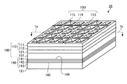
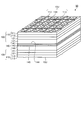
- FIG. 1 is a perspective view schematically showing a surface light source device according to the first embodiment of the present invention.
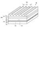
- FIG. 2 is a cross-sectional view showing a cross section of the surface light source device shown in FIG. 1 cut along a plane passing through line 1a-1b in FIG. 1 and perpendicular to the light output surface of the device.
- FIG. 3 is a perspective view schematically showing a surface light source device according to the second embodiment of the present invention.
- FIG. 4 is a cross-sectional view schematically showing an example of a metal mold forming method for producing a multilayer body used in the present invention.
- FIG. 5 is a cross-sectional view schematically showing an example of a metal mold formed by the forming method shown in FIG. FIG.
- FIG. 6 is a cross-sectional view schematically showing an example of a metal mold formed by another forming method.
- FIG. 7 is a cross-sectional view schematically showing an example of a metal mold formed by yet another forming method.
- FIG. 8 is a cross-sectional view schematically showing an example of a metal mold formed by yet another forming method.
- FIG. 9 is an enlarged partial top view showing the structure of the device light exit surface 10U of the surface light source device 10 shown in FIG.
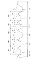
- FIG. 10 is a partial cross-sectional view showing a cross section of the concavo-convex structure layer 111 shown in FIG. 9 taken along a vertical plane passing through the line 10a of FIG.
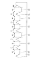
- FIG. 11 is a partial cross-sectional view showing a wider area of the cross section shown in FIG.
- FIG. 10 is a partial cross-sectional view.
- FIG. 12 is a partial cross-sectional view showing a modification of the recess shown in FIG.
- FIG. 13 is a partial cross-sectional view showing another modification of the recess shown in FIG.
- FIG. 14 is a perspective view schematically showing the surface light source device manufactured in Comparative Example 1.
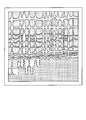
- FIG. 15 is a top view schematically showing rainbow unevenness observed on the device light exit surface of the conventional surface light source device.
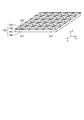
- FIG. 16 is a perspective view schematically showing a surface light source device according to the fourth embodiment of the present invention.
- FIG. 17 is a perspective view schematically showing the reflector composite substrate manufactured in Example 5.
- FIG. 12 is a partial cross-sectional view showing a modification of the recess shown in FIG.
- FIG. 13 is a partial cross-sectional view showing another modification of the recess shown in FIG.
- FIG. 14 is a perspective view schematically showing the surface light source device manufactured in Comparative Example 1.
- FIG. 15
- the surface light source device of the present invention includes an organic EL element including a light-emitting layer, and a light-emitting surface structure layer that is provided in contact with at least one surface of the organic EL element and defines a concavo-convex structure on the device light-emitting surface side.
- the device light exit surface is a light exit surface as a surface light source device, that is, a light exit surface when light exits from the surface light source device to the outside of the device.
- the device light exit surface is a surface parallel to the light emitting layer of the organic EL element, and is parallel to the main surface of the surface light source device.
- the surface on the concave portion described later can form an angle non-parallel to the light emitting layer.
- being parallel (or perpendicular) to the device exit surface viewed ignoring such recess is simply referred to as “parallel (or perpendicular) to the device exit surface”.
- the surface light source device will be described in a state where the device light-emitting surface is placed so as to be parallel to the horizontal direction and upward.
- the fact that each component is “parallel” or “vertical” may include an error within a range that does not impair the effects of the present invention, for example, an error of ⁇ 5 ° from a parallel or vertical angle. May be included.
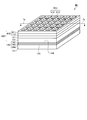
- FIG. 1 is a perspective view schematically showing a surface light source device according to a first embodiment of the present invention.
- the surface light source device 10 is a device having a rectangular flat plate structure having a device light exit surface 10U.
- FIG. 2 is a cross-sectional view showing a cross section of the surface light source device 10 shown in FIG. 1 taken along a plane passing through a line 1a-1b in FIG. 1 and perpendicular to the device light exit surface.
- the surface light source device 10 includes an organic EL element 140 and a light-emitting surface structure layer 100 provided in contact with the surface 144 of the organic EL element 140 on the device light-emitting surface 10U side.
- the surface light source device 10 further includes a sealing substrate 151 as an optional component on the surface 145 side of the organic EL element 140 opposite to the device light exit surface 10U.
- the organic EL element 140 includes a first electrode layer 141, a light emitting layer 142, and a second electrode layer 143.
- the first electrode layer 141 is a transparent electrode
- the second electrode layer 143 is a reflective electrode.
- the light exit surface structure layer 100 includes a multilayer body 110 including the concavo-convex structure layer 111 and the base film layer 112, a glass substrate 131 as a substrate, and an adhesive layer 121 that bonds the multilayer body 110 and the glass substrate 131. .
- the uneven structure layer 111 is located on the upper surface of the surface light source device 10 (that is, the outermost layer on the light output surface side of the surface light source device 10). Further, the concavo-convex structure layer 111 includes a plurality of concave portions 113, a flat portion 114 positioned around the concave portions 113, and the flat portion 114 having a height (that is, a position in the height direction when the device light-emitting surface is in the horizontal direction). ) Have a concavo-convex structure including different flat portions 115.
- the light exit surface 10U is defined by the uneven structure.
- the device light-emitting surface 10U is parallel to the other portions of the device such as the flat portions 114 and 115 and the glass substrate 131 when viewed macroscopically, ignoring the unevenness due to the difference in height between the concave portion 113 and the flat portions 114 and 115. Although it is a flat surface, it is an uneven surface including a slope defined by the recess 113 microscopically. In the present application, since the drawings are schematic illustrations, only a small number of recesses are shown on the device light-emitting surface. However, in an actual device, a single device light-emitting surface is shown here. A much larger number of recesses can be provided.
- the organic EL element 140 includes two or more electrode layers and a light emitting layer that is provided between these electrode layers and emits light when a voltage is applied from the electrode layers. And an element comprising:
- An organic EL element forms layers such as an electrode layer and a light emitting layer constituting the element on a substrate, and further provides a sealing member that covers those layers, and seals the layer such as the light emitting layer with the substrate and the sealing member.
- the element that emits light from the substrate side here is called a bottom emission type
- the element that emits light from the sealing member side is called a top emission type.
- the surface light source device of the present invention may be any of these, and in the case of a bottom emission type, a combination of a substrate for forming a layer and an optional layer as necessary is a light emitting surface structure layer.
- a combination including a light emitting surface side structure such as a sealing member and an optional layer as necessary constitutes a light emitting surface structure layer.
- the light emitting layer constituting the organic EL element is not particularly limited, and a known one can be appropriately selected.
- the light-emitting material in the light-emitting layer is not limited to one type, and the light-emitting layer is not limited to one layer, and may be a single layer or a combination of a plurality of layers in order to suit the use as a light source. Thereby, light of white or a color close thereto can be emitted.
- the organic EL device may further include other layers such as a hole injection layer, a hole transport layer, an electron transport layer, an electron injection layer, and a gas barrier layer in addition to the light emitting layer between the electrode layers.
- the organic EL element can further include arbitrary components such as a wiring for energizing the electrode layer and a peripheral structure for sealing the light emitting layer.
- the electrode layer of the organic EL element is not particularly limited and can be appropriately selected from known ones.
- both electrode layers can be made into a transparent electrode, and it can be set as the organic EL element (what is called see-through type) which emits light from both the light emission surface structure layer side and the opposite side.
- both electrode layers are transparent electrodes as described above, a reflecting member or a scattering member (for example, a white scattering member disposed via an air layer) is provided on the side opposite to the light-emitting surface structure layer.
- a reflecting member or a scattering member for example, a white scattering member disposed via an air layer
- ITO etc. can be mentioned as a material of a transparent electrode.
- the material for the hole injection layer include a starburst aromatic diamine compound.
- the material for the hole transport layer include triphenyldiamine derivatives.
- the host material for the yellow light-emitting layer include triphenyldiamine derivatives, and examples of the dopant material for the yellow light-emitting layer include tetracene derivatives.
- the material for the green light emitting layer include pyrazoline derivatives.
- Examples of the host material for the blue light emitting layer include anthracene derivatives, and examples of the dopant material for the blue light emitting layer include perylene derivatives.
- a material for the red light emitting layer a europium complex or the like can be used.
- Examples of the material for the electron transport layer include an aluminum quinoline complex (Alq).
- Examples of the cathode material include lithium fluoride and aluminum, which are sequentially stacked by vacuum film formation.
- a light emitting layer that generates a light emission color having a complementary color relationship which is called a laminated type or a tandem type, can be obtained by appropriately combining the above or other light emitting layers.
- the combination of complementary colors can be yellow / blue, green / blue / red, or the like.
- the light exit surface structure layer 100 may be composed of a plurality of layers, but may be composed of a single layer. From the viewpoint of easily obtaining a light-emitting surface structure layer having desired characteristics, it is preferably composed of a plurality of layers.
- corrugated structure layer and the base film layer can be included. Thereby, a light-emitting surface structure layer with high performance can be easily obtained.
- the resin composition constituting the concavo-convex structure layer and the base film can be a composition containing a transparent resin. That the transparent resin is “transparent” means that it has a light transmittance suitable for use in an optical member.
- each layer constituting the light exit surface structure layer can have a light transmittance suitable for use in an optical member, and the light output surface structure layer as a whole has a total light transmittance of 80% or more. It can have.
- the material of the transparent resin contained in the resin composition is not particularly limited, and various resins that can form a transparent layer can be used. Examples thereof include a thermoplastic resin, a thermosetting resin, an ultraviolet curable resin, and an electron beam curable resin.
- thermoplastic resins are preferable because they can be easily deformed by heat, and ultraviolet curable resins have high curability and high efficiency, so that an uneven structure layer can be formed efficiently.
- thermoplastic resin include polyester-based, polyacrylate-based, and cycloolefin polymer-based resins.
- ultraviolet curable resin include epoxy resins, acrylic resins, urethane resins, ene / thiol resins, and isocyanate resins. As these resins, those having a plurality of polymerizable functional groups can be preferably used.
- a material having a high hardness at the time of curing is preferable from the viewpoint of easily forming the concavo-convex structure on the light emitting surface of the device and easily obtaining scratch resistance of the concavo-convex structure.
- a material having a pencil hardness of HB or higher is preferable, and a material of H or higher is more preferable. The material which becomes 2H or more is more preferable.
- the material of the base film layer has a certain degree of flexibility in order to facilitate the handling of the multilayer body when forming the concavo-convex structure layer and / or after forming the multilayer body.
- a multilayer body that is easy to handle and excellent in durability can be obtained, and as a result, a high-performance surface light source device can be easily manufactured.
- Such a combination of materials can be obtained by appropriately selecting the transparent resin exemplified above as the resin constituting each material.
- an ultraviolet curable resin such as acrylate is used as the transparent resin constituting the material of the concavo-convex structure layer, while the alicyclic olefin polymer film (described later) is used as the transparent resin constituting the material of the base film.
- Zeonor film or the like) or polyester film can be used, and a preferable combination of materials can be obtained.
- the refractive index of the concavo-convex structure layer and the substrate film should be as close as possible, preferably the refractive index The difference is within 0.1, more preferably within 0.05.
- the resin composition that is a material of the layer that is a constituent element of the light-exiting surface structure layer such as the uneven structure layer and the base film layer can contain an optional component as necessary.
- the optional component include additives such as phenol-based and amine-based deterioration inhibitors; surfactant-based, siloxane-based antistatic agents; triazole-based, 2-hydroxybenzophenone-based light-resistant agents; be able to.
- the thickness of the concavo-convex structure layer is not particularly limited, but is preferably 1 to 70 ⁇ m.
- the thickness of the concavo-convex structure layer is the distance between the surface on the substrate side where the concavo-convex structure is not formed and the flat portion of the concavo-convex structure.
- the thickness of the base film layer is preferably 20 to 300 ⁇ m.
- the light-emitting surface structure layer can further include a substrate such as the glass substrate 131 in the light-emitting surface structure layer 100, thereby giving the surface light source device rigidity to suppress deflection. Further, by providing a substrate that is excellent in the performance of sealing the organic EL element as a substrate and that can easily form the layers constituting the organic EL element in the manufacturing process in order, a surface light source The durability of the device can be improved and the manufacture can be facilitated.
- the material constituting the substrate resin can be cited in addition to glass.
- the refractive index of the substrate is not particularly limited, but can be 1.4 to 2.0.
- the thickness of the substrate is not particularly limited, but is preferably 0.1 to 5 mm.
- the light exit surface structure layer may further include an adhesive layer interposed between two layers in the light exit surface structure layer, such as between the multilayer body and the substrate.
- the adhesive that is the material of the adhesive layer is not only a narrowly defined adhesive (a so-called hot melt type adhesive having a shear storage modulus of 1 to 500 MPa at 23 ° C. and does not exhibit tackiness at room temperature), A pressure-sensitive adhesive having a shear storage modulus at 1 ° C. of less than 1 MPa is also included.
- a material having a refractive index close to that of the substrate and the transparent resin layer and being transparent can be used as appropriate. More specifically, an acrylic adhesive or a pressure-sensitive adhesive can be used.
- the thickness of the adhesive layer is preferably 5 to 100 ⁇ m.
- the concavo-convex structure on the light-emitting surface structure layer includes a plurality of concave portions including inclined surfaces and a flat portion positioned around the concave portion.
- the “slope” is a surface that forms an angle that is not parallel to the light output surface of the apparatus.
- the surface on the flat portion can be a surface parallel to the device light exit surface.
- the flat portion and / or the concave portion has a difference (dimension difference) exceeding a difference that causes interference of one or both of the emitted light and the reflected light at one or more of the width, height or depth and interval.
- the dimensional difference may be a dimensional difference exceeding the difference that causes interference of the emitted light, but the reflected light tends to have a greater influence on the rainbow unevenness than the emitted light. It is preferable that the size difference exceeds a difference that causes interference between the output light and the difference in size that exceeds a difference that causes interference between both outgoing light and reflected light.
- the height represents the height of the flat portion
- the depth represents the depth of the recess (that is, the position in the height direction when the device light-emitting surface is in the horizontal direction).
- the width of the flat portion corresponds to the interval between the concave portions
- the interval between the flat portions corresponds to the width of the concave portion.
- the dimensional difference may be only in the flat part, in the concave part, or in both the flat part and the concave part.
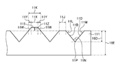
- FIG. 9 is an enlarged partial top view showing the structure of the device light exit surface 10U of the surface light source device 10 defined by the concavo-convex structure layer 111.
- FIG. 10 is a partial cross-sectional view showing a cross section of the concavo-convex structure layer 111 taken along a vertical plane passing through the line 10a of FIG.
- Each of the plurality of recesses 113 is a depression having a regular quadrangular pyramid shape. Therefore, the slopes 11A to 11D of the recess 113 have the same shape, and the bases 11E to 11H form a square. However, since the slope 11C is in a series with the slope 11W extending along the flat portion 115, the base 11G among the bases 11E to 11H does not appear as a structure with an uneven structure. In FIG. 9, such a base is indicated by a broken line.
- the line 10a is a line that passes over all the vertices 11P of the recesses 113 in a row, and is a line parallel to the bottom sides 11E and 11G of the recesses 113.
- the concave portions 113 are continuously arranged in two orthogonal arrangement directions at regular intervals.
- One of the two arrangement directions X is parallel to the bases 11E and 11G.
- the plurality of recesses 113 are aligned at intervals 11J or 11K.
- the other direction Y of the two arrangement directions is parallel to the bases 11F and 11H, and also in this direction Y, the plurality of recesses 113 are aligned at intervals 11J or 11K. Therefore, the width of the flat portion 114 is 11J, and the combined width of the flat portion 115 and the pair of inclined surfaces 11W extending along both sides of the flat portion is 11K.
- the angles formed by the inclined surfaces 11A to 11D constituting each of the concave portions 113 and the flat portion 114 are set to 60 °, for example.
- the apex angle of the regular quadrangular pyramid that is formed, that is, the angle formed by the opposing inclined surfaces at the apex 11P (the angle 11N shown in FIG. 10 for the angles formed by the inclined surfaces 11B and 11D) is also 60 °.
- the width 11J of the flat portion 114 and the width 11X of the flat portion 115 are set to be the same.
- the pitch 16A between the two flat portions 114 is equal to the sum of the length of the base of the quadrangular pyramid and the width of the flat portion 114
- the pitch 16B from the flat portion 114 to the flat portion 115 has the slope 11W.
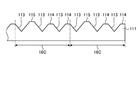
- the light-emitting surface structure layer 111 has a structure having a repeating unit 16C shown in FIG. Become. That is, in the cross section of the light exit surface structure layer 111, the repeating unit 16C including the two flat portions 114, the one flat portion 115, and the inclined surfaces (including the inclined surface 11W) of the three concave portions 113 existing therebetween is repeated. . In addition to the cross section passing through the line 10a shown in FIG. 9, this repetition can occur in a cross section perpendicular to the line 10a and perpendicular to the device light exit surface.
- one or more elements of the width, height or depth and interval of the flat portion and / or the concave portion are set with a dimensional difference exceeding the difference that causes interference of one or both of the emitted light and the reflected light.
- the dimensional difference exceeding the difference that causes interference is, for example, the dimension of 0.62 times or more, preferably 1.5 times or more of the center wavelength of the light emitted from the surface light source device. It is a difference, and by providing this dimensional difference, the occurrence of rainbow unevenness can be suppressed.
- the upper limit of such a dimensional difference is not particularly limited, but can preferably be 60 times or less the center wavelength of the light emitted from the surface light source device.
- the dimensional difference exceeding the difference that causes interference is usually 0.62 times or more, preferably at least 0.62 times the center wavelength of the light reflected to the outside of the surface light source device on the device light-emitting surface. Is a dimensional difference of 1.5 times or more, and usually a dimensional difference of 60 times or less.
- the above-mentioned dimensional difference may be set as the center wavelength of light that normally reflects the center wavelength of visible light of 550 nm.
- the dimensional difference between the flat part and / or the concave part may appear at random on the entire surface of the light exit surface of the device.
- the repeating unit such as the above-described repeating unit 16C in the cross section. It is preferable to have.
- the cross section has a repeating unit composed of two or more concave portions and two or more flat portions having different heights.
- the surface light source device has a configuration including a plurality of concave portions and flat portions located around the concave portion on the light exit surface of the device, thereby increasing light extraction efficiency and reducing changes in color depending on the observation angle.
- the surface light source device of the present invention has the above-described configuration, so that the displacement of at least one of the x-coordinate and y-coordinate of the chromaticity coordinate in all hemispherical directions on the light-emitting surface is not compared with the case where the above configuration is not used. Can be halved. For this reason, in the surface light source device, it is possible to suppress changes in color due to the observation angle.
- a chromaticity coordinate can be calculated from the emission spectrum measured in each direction by providing a mechanism that can rotate the angle from ⁇ 90 to 90 °, the displacement can be calculated.
- the ratio of the area occupied by the flat portion to the sum of the area occupied by the flat portion and the area occupied by the concave portion when the concavo-convex structure layer is observed from the direction perpendicular to the light exit surface of the device (hereinafter referred to as “flat portion ratio”).
- the light extraction efficiency of the surface light source device can be improved by appropriately adjusting. Specifically, when the flat portion ratio is 10 to 75%, good light extraction efficiency can be obtained, and the mechanical strength of the device light exit surface can be increased.
- the concave portion may have, for example, a cone shape, a partial spherical shape, a groove shape, and a combination thereof in addition to the pyramid shape described above.
- the shape is preferably a combination of pyramids.
- the pyramid shape may be a quadrangular pyramid having a square bottom surface as exemplified by the recess 113, but is not limited thereto, and may be a pyramid shape such as a triangular pyramid, a pentagonal pyramid, a hexagonal pyramid, or a quadrangular pyramid having a non-square base. You can also.
- the pyramid as used in the present application includes not only a normal pyramid with a sharp top but also a rounded tip or a flat chamfered shape (such as a truncated cone shape).
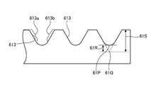
- the top portion 11P of the quadrangular pyramid has a pointed shape, but this may have a rounded shape like the top portion 61P of the concave portion 613 shown in FIG.
- a flat portion 71 ⁇ / b> P may be provided at the top of the pyramid to form a flat chamfered shape.
- the height difference 61R between the top 61P and the top 61Q when the pyramid has a rounded and sharp shape is The pyramid can be 20% or less of the height 61S of the pyramid when the pyramid has a rounded and sharp shape.
- the height of the flat portion 71P and the top 71Q when the top of the pyramid is not flat but sharp.
- the difference 71R can be 20% or less of the height 71S of the pyramid when the apex of the pyramid is not flat but sharp.
- the depth of the concave portion in the concavo-convex structure is not particularly limited, but the average roughness of the center line measured on the surface on which the concavo-convex structure is formed along various directions (various directions in a plane parallel to the device light exit surface).
- the maximum value (Ra (max)) can be in the range of 1 to 50 ⁇ m.
- the thickness of the concavo-convex structure layer increases the flexibility of the multilayer body. Handling of the multilayer body in the manufacturing process of the light source device is facilitated. Specifically, the difference between the depth 16D of the recess shown in FIG. 10 (the height from the vertex 11P to the average level of the flat portions 114 and 115) and the thickness 16E of the concavo-convex structure layer 111 is 0 to 30 ⁇ m. It is preferable.
- the angle formed by the slope of the recess and the light exit surface is preferably 40 to 70 °, and more preferably 45 to 60 °.
- the apex angle (corner 11N in FIG. 10) is preferably 60 to 90 °.
- the angle formed by the inclined surface and the device light exit surface is large.
- the angle is preferably 55 ° or more, and more preferably 60 ° or more.
- the upper limit of the angle can be about 70 ° in consideration of maintaining the durability of the uneven structure layer.
- the angle of the slope other than the rounded or chamfered part is the angle of the slope.
- the surfaces 613 a, 613 b, 713 a, and 713 b are pyramid slopes. By setting the angle of the slope to such an angle, the light extraction efficiency can be increased.
- the slopes of the concavo-convex structure need not all have the same angle, and slopes having different angles may coexist within the above range.
- the plurality of recesses can be arranged in any manner on the device light exit surface.
- a plurality of recesses can be arranged along two or more directions on the device light exit surface. More specifically, they can be arranged along two orthogonal directions like the recesses 113 shown in FIGS.
- a gap between adjacent concave portions is provided in one or more directions among them, and a flat portion can be constituted by the gap.
- a gap between adjacent concave portions is provided in one or more directions among them, and a flat portion can be constituted by the gap.
- gaps of intervals 11J and 11K are provided in two orthogonal directions, and the flat parts 114 and 115 are constituted by the gaps.
- the manufacturing method of the surface light source device of the present invention is not particularly limited, when manufacturing the surface light source device including the light emitting surface structure layer having the concavo-convex structure layer, the base film, the adhesive layer, and the glass substrate exemplified above, Each layer constituting the organic EL element is laminated on one surface of the glass substrate, and thereafter or before that, a multilayer body having a concavo-convex structure layer and a base film on the other surface of the glass substrate is interposed via an adhesive layer. It can be manufactured by sticking.
- the production of a multilayer body having a concavo-convex structure layer and a base film can be carried out by preparing a mold such as a metal mold having a desired shape and transferring it to a material layer forming the concavo-convex structure layer. .
- Method 1 A raw multilayer having a layer of the resin composition A constituting the base film and a layer of the resin composition B constituting the concavo-convex structure layer (the concavo-convex structure is not yet formed) is prepared, A method of forming a concavo-convex structure on the surface of the unprocessed multilayer body on the resin composition B side; and (Method 2) A resin composition B in a liquid state was applied on the base film and applied. A method may be mentioned in which a mold is applied to the layer of the resin composition B, the resin composition B is cured in that state, and a concavo-convex structure layer is formed.
- the raw multilayer body can be obtained by, for example, extrusion molding in which the resin composition A and the resin composition B are coextruded.
- An uneven structure can be formed by pressing a mold having a desired surface shape onto the surface of the unprocessed multilayer body on the resin composition B side. More specifically, a long raw multilayer body is continuously formed by extrusion molding, and the raw multilayer body is pressed with a transfer roll and a nip roll having a desired surface shape, thereby continuously. Manufacturing can be performed efficiently.
- the clamping pressure between the transfer roll and the nip roll is preferably several MPa to several tens of MPa.
- the temperature at the time of transfer is preferably Tg or more (Tg + 100 ° C.) or less, where Tg is the glass transition temperature of the resin composition B.
- the contact time between the unprocessed multilayer body and the transfer roll can be adjusted by the film feed speed, that is, the roll rotation speed, and is preferably 5 seconds or more and 600 seconds or less.
- Method 2 it is preferable to use a composition that can be cured by energy rays such as ultraviolet rays as the resin composition B constituting the concavo-convex structure layer.
- energy rays such as ultraviolet rays
- energy rays such as ultraviolet rays
- a molding method in which a metal substrate is cut with a cutting tool, and an unevenness is formed on a resin plate with a laser or the like As the molding method of the mold used in the production of the multilayer body used in the present invention by the method 1 and the method 2, etc., a molding method in which a metal substrate is cut with a cutting tool, and an unevenness is formed on a resin plate with a laser or the like. And a method of forming a mold by processing it and using it as a prototype. From the viewpoint of processing accuracy and ease of processing, a molding method in which a metal substrate is cut with a cutting tool can be given as a particularly preferable example.
- FIG. 4 is a cross-sectional view schematically showing an example of a metal mold forming method for producing a multilayer body used in the present invention.
- FIG. 4 shows a process of forming linear grooves arranged in parallel with a cutting tool 961 on one surface of a metal plate 911 being processed into a metal mold.
- 4 shows a cross-sectional view of the metal plate 911 cut along a plane perpendicular to the extending direction of the groove.
- the surface of the metal plate 911 is cut with the cutting tool 961 to first form the groove 915 at the right end in FIG. 4, and then the cutting position of the cutting tool 961 is moved upward by a length of 96 A and the arrow
- the adjacent groove 914 is formed by moving the length 96B in the A1 direction.
- the cutting position of the cutting tool 961 is moved by the length 96C in the direction of the arrow A1, and the adjacent groove 914 is formed.
- the bottom surface of the groove 914 and the bottom surface of the groove 915 are flat surfaces corresponding to the flat surfaces 114 and 115, respectively.
- the convex portion 913 on the cutting surface is a portion corresponding to the concave portion 113.
- the width W1 of the bottom surfaces of the grooves 914 and 915 corresponds to the shape of the cutting surface of the cutting tool 961, and the distances P1 and P2 between the bottom surfaces are the movement distances, respectively.
- the distance is obtained by subtracting the width W1 from 96B and 96C.
- FIG. 6 shows a state in which grooves 924 and 925 are formed on the metal plate 921 using two types of cutting tools having different shapes, respectively.
- the grooves 924 and 925 have the same bottom width W1, but by using different tools, the inclined angles 92M and 92L of the inclined surfaces in the grooves are different.
- the distance between the bottom surfaces of the grooves is also set to a constant distance P1.
- grooves having different depths such as grooves 934 and 935 on the metal plate 931 shown in FIG. 7, are formed by a common bite, and only the height of the flat portion or the depth of the recess is different ( It is also possible to form a shape having a dimension difference). In this case, in the resulting concavo-convex structure layer, the depths of the vertices of the recesses are non-uniform.
- the shape of the recess constituting the device light exit surface is not limited to the pyramid shape exemplified as the first embodiment, and for example, a groove shape as in the second embodiment shown below. It may be a shape.
- FIG. 3 is a perspective view schematically showing a surface light source device according to the second embodiment of the present invention. As shown in FIG. 3, the surface light source device 30 according to the second embodiment is different in the shape of the device light exit surface, that is, the shape of the surface of the concavo-convex structure layer 311 in the multilayer body 310 constituting the light exit surface structure layer 300. Others have the same configuration as the first embodiment.
- Each of the plurality of recesses 313 formed on the surface of the concavo-convex structure layer 311 has a linear, groove-like shape and two flat slopes.
- a cross section cut by a plane perpendicular to the cross section has a triangular shape having two hypotenuses.
- the plurality of recesses 313 are arranged in parallel on the device light exit surface 30U. Crevices 314 and 315 having different heights are provided between the adjacent recesses 313, and the gaps 314 and 315 form a flat part on the device light exit surface 30U.
- the groove-like shape of the recess is not particularly limited as long as it includes an inclined surface, and the cross section exemplified above is not limited to a triangular shape, and can take various shapes.
- the cross-sectional shape of the groove may be another polygonal shape such as a pentagon or a heptagon, or a shape other than a polygon such as a part of a circle.
- the top of the pyramid or cone is shaped like a rounded shape or a flat chamfered shape. The shape may be transformed into a shape with rounded vertices or a flat chamfered shape.
- the flat part of the light exit surface of the device is composed of two groups of a flat part having a low height (114 or 314) and a flat part having a high height (115 or 315). Therefore, the height of the flat portion was only two types, but the present invention is not limited to this, and the difference in height (dimensional difference) of the flat portion is, for example, as in the third embodiment shown below. There may be three or more types and three or more flat portions having different heights may be provided.
- FIG. 8 is a partial cross-sectional view schematically showing an aspect of forming a groove for forming a metal mold for forming a concavo-convex structure on the device light-emitting surface in a surface light source device according to a third embodiment of the present invention. It is.
- the metal mold 941 is formed with five types of grooves using the same shape of cutting tool. Each groove has one of five widths W31 to W35. The bottom of the groove having the width W31 is at a level 946 which is shallower by the height A94 than the average line 944 of the depth of the groove, and the bottom of the groove having the width W32 is A93 higher than the average line 944 of the depth of the groove.
- the bottom of the groove having the width W33 is at the level 944 of the groove depth average line, and the groove having the width W34 is a height A91 minutes higher than the groove depth average line 944.
- the bottom of the groove having the depth 943 and the width W35 is at the level 942 deeper than the average depth 944 of the groove by a height A92.
- the heights A91 and A93 are equal, the heights A92 and A94 are equal, and A91 and A93 are half of A92 and A94, that is, the five groups of grooves are equally spaced apart (dimensions). There are five different depths.
- a set of such five kinds of grooves arranged at random constitutes a unit W36, and a shape in which these units are repeated is provided.
- the groove having such a shape along a certain direction in the surface of the metal mold and subsequently forming the groove along a direction orthogonal to the direction five types of the pyramid-shaped concave portion and its surroundings are formed.
- a metal mold capable of forming a concavo-convex structure composed of five groups of flat portions having different heights can be formed.
- the height differences (dimension differences) between the groups are respectively the emitted light and the reflected light. It is preferable that the difference (dimension difference) exceeds the difference that causes one or both of the interferences.
- the difference is preferably a ratio that represents a difference (dimension difference) exceeding a difference that causes interference of one or both of the emitted light and the reflected light.
- the rainbow unevenness can be more effectively reduced by including three or more flat portions having a dimensional difference exceeding a difference that causes interference of one or both of the emitted light and the reflected light.
- the rainbow unevenness can be reduced more effectively in the same manner by having three or more concave portions having a dimensional difference exceeding the difference that causes interference of one or both of the emitted light and the reflected light.
- ⁇ Fourth Embodiment> In the first to third embodiments described above, only one surface of the surface light source device is used as the device light-emitting surface. However, the present invention is not limited to this. For example, as in the following fourth embodiment, a surface is used. Both surfaces of the light source device may be used as the device light exit surface.
- FIG. 16 is a perspective view schematically showing a surface light source device according to the fourth embodiment of the present invention.
- the surface light source device 50 according to the fourth embodiment includes a second electrode layer 146 that is a transparent electrode instead of the second electrode layer 143 that is a reflective electrode, and a light exit surface instead of the sealing substrate 151. Except for the point provided with the structural layer 100, it has the same structure as 1st embodiment. Therefore, in the surface light source device 50 of the present embodiment, the light exit surface structure layer 100 is provided so as to be in contact with both the surfaces 144 and 145 of the organic EL element 140.
- the second electrode layer 146 is a transparent electrode, the light from the light emitting layer 142 passes through the first electrode layer 141 and the second electrode layer 146 and is emitted from both the upper and lower devices in the figure. Light exits from the surface 10U. Even when light is emitted from both the front surface and the back surface, advantages similar to those of the first embodiment can be obtained.
- the surface light source device 50 of the present embodiment normally, light incident on one device light exit surface 10U is transmitted through the surface light source device 50 and emitted from the other device light exit surface 10U. Accordingly, the opposite side can be seen with the naked eye through the surface light source device 50, and a see-through surface light source device can be realized, so that the design can be diversified.
- the light emitting surface structure layer is the same as that of the first embodiment, but the structure of the light emitting surface structure layer is not limited to this, and for example, the second or third embodiment.
- the light-emitting surface structure layer described in (1) may be adopted.
- an example in which the same light exit surface structure layer 100 is provided on both the upper surface 144 and the lower surface 145 of the organic EL element 140 in the drawing is shown, but different light exit surface structure layers may be provided in combination.
- the light output surface structure layer 100 similar to that of the first embodiment is provided on the surface 144 of the first electrode layer 141
- the organic EL element when light is emitted from both surfaces 144 and 145 of the organic EL element using a transparent electrode as the second electrode layer 146, if a light exit surface structure layer is provided on at least one surface, The light-emitting surface structure layer may not be provided on the other surface.
- the lighting fixture of the present invention and the backlight device of the present invention both include the surface light source device of the present invention.
- the lighting fixture of the present invention has the surface light source device of the present invention as a light source, and can further include arbitrary components such as a member for holding the light source and a circuit for supplying power.
- the backlight device of the present invention has the surface light source device of the present invention as a light source, and further includes a housing, a circuit for supplying electric power, a diffusion plate for making light emitted more uniform, a diffusion sheet, a prism sheet, etc. Optional components.
- the backlight device of the present invention can be used as a backlight of a display device such as a liquid crystal display device that displays an image by controlling pixels and a display device that displays a fixed image such as a signboard.
- the light emitting surface structure layer is composed of a concavo-convex structure layer, a base film layer, an adhesive layer, and a glass substrate, but the light emitting surface structure layer is a layer having fewer layers than these. It may be configured from the above, or conversely, an arbitrary layer may be further included in addition to these layers.
- a coating layer may be further provided on the concavo-convex structure layer, and this may define the concavo-convex structure on the device light exit surface.
- the concave portions distributed on the entire surface of the device light-emitting surface are shown as those having only the same shape distributed.
- concave portions having different shapes are mixed on the light-emitting surface of the device. May be.
- pyramid-shaped concave portions having different sizes may be mixed, or a combination of a plurality of pyramids and a simple pyramid shape may be mixed.
- the rainbow nonuniformity by interference can be suppressed similarly to the case where a difference (dimensional difference) is provided in the height of a flat part, or the depth of a recessed part.
- the surface light source device of the present invention is configured such that the light emission surface structure is more than the organic EL element as a layer constituting a part or all of the light emission surface structure layer for the purpose of further enhancing light extraction efficiency and viewing angle characteristics.
- a diffusion member that diffuses and transmits or reflects incident light may be further included.
- a part or the whole of the light exit surface structure layer may have a function as a diffusion member, and a separate member as a diffusion member is provided separately from the light exit surface structure layer. May be.
- the reflective electrode layer in illustration of the said embodiment, even if it replaces a reflective electrode with a transparent electrode, the rainbow nonuniformity by interference can be suppressed.
- the apparatus which has an effect similar to a reflective electrode can be comprised.
- the refractive index of the resin described below is the refractive index after curing.
- VK-9500 manufactured by Keyence Corporation
- Example 1 A surface light source device schematically shown in FIGS. 1 and 2 was produced and evaluated. However, in FIG. 1, an organic EL element 140 having only three layers is schematically illustrated. However, the surface light source device manufactured in this example includes an organic EL element including more light emitting layers. ing.
- a transparent electrode layer 100 nm On one main surface of a glass substrate having a thickness of 0.7 mm, a transparent electrode layer 100 nm, a hole transport layer 10 nm, a yellow light emitting layer 20 nm, a blue light emitting layer 15 nm, an electron transport layer 15 nm, an electron injection layer 1 nm, and a reflective electrode layer 100 nm. Were formed in this order.
- the hole transport layer to the electron transport layer were all made of an organic material.
- the yellow light emitting layer and the blue light emitting layer have different emission spectra.
- each layer from the transparent electrode layer to the reflective electrode layer is as follows: -Transparent electrode layer; tin-added indium oxide (ITO) Hole transport layer: 4,4′-bis [N- (naphthyl) -N-phenylamino] biphenyl ( ⁇ -NPD) ⁇ Yellow luminescent layer: 1.5% by weight of rubrene added ⁇ -NPD Blue light emitting layer: 10% by weight of iridium complex added 4,4′-dicarbazolyl-1,1′-biphenyl (CBP) -Electron transport layer; phenanthroline derivative (BCP) -Electron injection layer; lithium fluoride (LiF) -Reflective electrode layer: Al
- the transparent electrode layer was formed by a reactive sputtering method using an ITO target, and the surface resistance was 10 ⁇ / ⁇ or less.
- the formation from the hole injection layer to the reflective electrode layer is carried out by placing a glass substrate on which a transparent electrode layer has already been formed in a vacuum evaporation apparatus, and successively using the resistance heating method for the materials from the hole transport layer to the reflective electrode layer. This was done by vapor deposition.
- the system internal pressure was 5 ⁇ 10 ⁇ 3 Pa, and the evaporation rate was 0.1 to 0.2 nm / s.
- the obtained organic EL element had a rectangular light-emitting surface capable of emitting white light from the glass substrate side.
- the metal mold was pressed and irradiated with ultraviolet light from the base film side with an integrated light quantity of 1000 mJ / cm 2 to form a concavo-convex structure layer on the base film, and the layer structure of the base film 112 and the concavo-convex structure layer 111 was formed.
- the multilayer body 110 which is a rectangular film having the above was obtained.
- the concavo-convex structure on the concavo-convex structure layer 111 was composed of a plurality of regular quadrangular pyramid-shaped recesses 113 and flat portions 114 and 115 located around the recesses, as shown in FIGS.
- the angle (11L, 11M, etc.) formed by the inclined surface forming the recess 113 and the flat portion was 60 °.
- the length of the bottom sides (11E to 11H) of the recess 113 is 16 ⁇ m
- the width 11J of the flat portion 114 between the recesses 113 is 4 ⁇ m
- the width 11X of the flat portion 115 is 4 ⁇ m, both at regular intervals. there were.
- the height difference (dimension difference) between the flat portion 114 and the flat portion 115 was 2 ⁇ m.
- the bottom side of the recess 113 was parallel to the long side or short side direction of the multilayer body 110.
- the thickness of the concavo-convex structure layer 111 (the thickness from the average height of the flat portions 114 and 115 to the surface in contact with the base film) was 34 ⁇ m, and the thickness of the base film layer 112 was 100 ⁇ m.
- the flat portion ratio was 36%.
- the multilayer body 110 obtained in (1-2) is bonded with an adhesive (acrylic resin, refractive index 1.49, A surface light source device including a multilayer structure 110-adhesive layer 121-glass substrate 131-organic EL element 140 was obtained by pasting through Nitto Denko Corporation CS9621). The thickness of the adhesive layer was 20 ⁇ m.
- ⁇ Comparative Example 1> In preparing the multilayer body of (1-2) above, a multilayer body was prepared in the same manner as in Example 1, except that the shape of the metal mold was changed, and a surface light source device was obtained. In the obtained multilayer body, the shape of the concave portion was substantially the same as that in Example 1, but the flat portion was composed of only the flat portion 414 having a uniform height as shown in FIG. It was. When the obtained surface light source device was observed under the same conditions as in (1-4) of Example 1, it was observed that rainbow unevenness as shown in FIG. 15 occurred.
- Example 2 In the preparation of the multilayer body 110 of (1-2) above, the multilayer body 110 was prepared in the same manner as in Example 1 except that the shape of the metal mold was changed, and a surface light source device was obtained.
- the uneven shape of the light exit surface of the device has five groups of flat surfaces having different heights. That is, in the molding of the mold, the repeating unit W36 shown in FIG. 8 is formed along one in-plane direction on one surface of the metal plate to be the mold, and then along the direction orthogonal to the direction. Formed and formed a mold.
- Example 1 When the obtained surface light source device was observed under the same conditions as in Example 1-4 (1-4), it was observed that it was in a good state with less rainbow unevenness than Example 1.
- Example 3 In preparing the multilayer body 110 of (1-2) above, the multilayer body 110 was prepared in the same manner as in Example 1 except that the metal mold was changed, and a surface light source device was obtained. In Example 3, the metal mold used in Example 1 was subjected to nickel electroforming, to prepare a metal mold having a surface with an inverted concavo-convex structure, and this prepared metal mold was used. .
- Example 1 When the obtained surface light source device was observed under the same conditions as in (1-4) of Example 1, it was observed that it was in a good state with less rainbow unevenness than Example 1.
- Example 4> Formation of transparent organic EL element
- a hole injection layer, a hole transport layer, a light emitting layer, a hole blocking layer, a charge generation layer, a metal oxide layer, and a cathode layer were formed in this order on a glass substrate having a transparent electrode layer formed on the main surface.
- the material and film thickness for forming each layer are as follows.
- -Transparent electrode layer ITO 300nm
- Hole injection layer Molybdenum trioxide (MoO 3 ) 5 nm
- Hole transport layer NS21 [manufactured by Nippon Steel Chemical Co., Ltd.] and MoO 3 20 nm, NS212 5 nm, total 25 nm -Light emitting layer: NS21 and EY52 (both manufactured by e-Ray Optoelectronics Technology (hereinafter referred to as e-Ray)) 20 nm, EB43 and EB52 (both manufactured by e-Ray) 30 nm, total 50 nm
- Hole blocking layer bis (2-methyl-8-quinolinolato) (p-phenylphenolate) aluminum (BAlq) 5 nm
- Charge generation layer Liq and DPB 35 nm, aluminum 1.5 nm, NS21 and MoO 3 10 nm, total 37.5 nm
- Metal oxide layer MoO 3 5 nm -Cath
- a glass substrate on which a transparent electrode layer has already been formed is placed in a vacuum evaporation apparatus, and the materials from the hole transport layer to the metal oxide layer are sequentially applied by resistance heating. This was done by vapor deposition. System pressure is 5 ⁇ 10 -3 Pa, it was carried out at evaporation rate 0.1 ⁇ 0.2nm / s. Thereafter, ITO of the cathode layer was formed by facing target sputtering. This was sealed with another glass plate using a UV curable resin to obtain a transparent organic EL element 1. The obtained transparent organic EL element 1 emitted white light from both directions.
- a multilayer body 110 was prepared in the same manner as in Example 2 except that the shape of the metal mold was changed in the preparation of the multilayer body 110 of (1-2) above. Next, this multilayer body 110 was bonded to the transparent organic EL element 1 obtained in the above (1-5) to obtain a surface light source device.
- the width 11X of the flat portion 114 and the width 11J of the flat portion 115 shown in FIGS. 9 and 10 were each 8 ⁇ m.
- Example 1 When the obtained surface light source device was observed under the same conditions as in (1-4) of Example 1, it was observed that it was in a good state with little rainbow unevenness as in Example 1.
- Example 5> (1-6: Production of organic EL element with reflecting member)
- ⁇ Production Example 1 Production of reflective member>
- a metal mold having a predetermined shape is pressed onto the coating film, and ultraviolet rays are irradiated from the base film side with an integrated light amount of 1000 mJ / cm 2 to cure the coating film, and the uneven structure portion is formed on the base film. Formed.
- the metal mold was peeled off from the concavo-convex structure portion to obtain a reflecting portion composite substrate composed of the base film and the concavo-convex structure portion.
- FIG. 17 is a perspective view schematically showing the reflector composite substrate manufactured in Example 5.
- the concavo-convex structure on the surface of the concavo-convex structure part of the obtained reflective part composite substrate 147 was composed of a plurality of regular quadrangular pyramidal concave parts 14Z as schematically shown in FIG.
- the angle formed by the inclined surfaces 14A to 14D constituting the recess 14Z with the surface of the base film was 30 °.
- the length of the bottom side 14E of the recess 14Z was 20 ⁇ m, and the recess 14Z had a structure arranged at a pitch of 20 ⁇ m in two orthogonal directions X and Y on the surface of the concavo-convex structure portion.
- the total thickness of the reflection part composite substrate 147 was 200 ⁇ m.
- a metal reflective layer was formed by vapor-depositing silver with a thickness of 200 nm on the surface of the reflective portion composite substrate obtained in (1-6) above where the concavo-convex structure was formed. Thereby, the reflection part composite body which consists of a reflection part composite substrate and the reflection layer which has an uneven structure was obtained.
- the reflective part composite obtained in the above (1-7) is bonded with an adhesive (acrylic resin, refractive index 1.49). , Manufactured by Nitto Denko Corporation (CS9621) to obtain an organic EL element with a reflective member.
- the multilayer body produced in Example 2 was pasted on the light-emitting surface side of the obtained organic EL element with a reflecting member via an adhesive (acrylic resin, refractive index 1.49, manufactured by Nitto Denko Corporation CS9621), A surface light source device was obtained.
- Example 1 When the obtained surface light source device was observed under the same conditions as in (1-4) of Example 1, it was observed that it was in a good state with little rainbow unevenness as in Example 1.
Landscapes
- Physics & Mathematics (AREA)
- Optics & Photonics (AREA)
- General Physics & Mathematics (AREA)
- Electroluminescent Light Sources (AREA)
- Optical Elements Other Than Lenses (AREA)
- Planar Illumination Modules (AREA)
Abstract
Description
〔1〕 発光層を含む有機エレクトロルミネッセンス素子と、前記有機エレクトロルミネッセンス素子の少なくとも一方の表面に接して設けられる出光面構造層と、を備える面光源装置であって、
前記出光面構造層は、当該装置出光面側の表面に凹凸構造を有し、
前記凹凸構造は、斜面を含む複数の凹部と、前記凹部の周囲に位置する平坦部とを有し、且つ
前記平坦部及び/または凹部には、その幅、高さもしくは深さ及び間隔の1以上の要素において、出射光及び反射光の一方又は両方の干渉をもたらす差異を超える寸法差が設けられている、面光源装置。
〔2〕 前記出光面構造層を、前記装置出光面に垂直で且つ前記凹部を通る平面で切断した断面において、前記装置出光面が、2以上の凹部及び2以上の平坦部からなる繰り返し単位を有する、前記面光源装置。
〔3〕 前記凹凸構造層を前記装置出光面に垂直な方向から観察した場合における、前記平坦部が占める面積と前記凹部が占める面積との合計に対する、前記平坦部が占める面積の割合が、10~75%である、前記面光源装置。
〔4〕 〔1〕~〔3〕のいずれか1項に記載の面光源装置を備える照明器具。
〔5〕 〔1〕~〔3〕のいずれか1項に記載の面光源装置を備えるバックライト装置。
〔6〕 発光層を含む有機エレクトロルミネッセンス素子と、前記有機エレクトロルミネッセンス素子の少なくとも一方の表面に接して設けられる出光面構造層と、を備える面光源装置であって、
前記出光面構造層は、当該装置出光面側の表面に凹凸構造を有し、
前記凹凸構造は、斜面を含む複数の凹部と、前記凹部の周囲に位置する平坦部とを有し、且つ
前記平坦部及び/または凹部には、その幅、高さもしくは深さ及び間隔の1以上の要素において、出射光の干渉をもたらす差異を超える寸法差が設けられている、面光源装置。
〔7〕 〔1〕または〔6〕に記載の面光源装置であって、
前記有機エレクトロルミネッセンス素子は、2層以上の電極層と、これらの電極層間に設けられ、電極層から電圧を印加されることにより発光する発光層と、を備え、
前記2層以上の電極層は、それぞれ透明電極からなる層である面光源装置。
本発明の照明器具及びバックライト装置は、前記本発明の面光源装置を有するので、光取り出し効率が高く、機械的強度が高く、出光面の虹ムラの発生が少なく、且つ容易に製造することができる照明器具及びバックライト装置とすることができる。
以下において、図面を参照して、本発明をより詳細に説明する。
本発明の面光源装置は、発光層を含む有機EL素子、および前記有機EL素子の少なくとも一方の表面に接して設けられ、装置出光面側の表面の凹凸構造を規定する出光面構造層を備える。
前記装置出光面とは、面光源装置としての出光面、即ち、面光源装置から装置外部に光が出光する際の出光面である。装置出光面は、前記有機EL素子の前記発光層と平行な面であり、面光源装置の主面と平行である。但し、微視的に見ると、後述する凹部上の面は発光層と非平行な角度をなしうる。以下、別に断らない限り、かかる凹部を無視して見た装置出光面と平行(又は垂直)であることを、単に「装置出光面と平行(又は垂直)」であるという。また、別に断らない限り、面光源装置は、かかる装置出光面が水平方向と平行で且つ上向きになるよう載置した状態で説明する。
本発明において、各構成要素が「平行」又は「垂直」であるとは、本発明の効果を損ねない範囲の誤差を含んでいてもよく、例えば、平行又は垂直な角度から±5°の誤差を含んでいてもよい。
前記有機EL素子140として例示するように、本発明において、有機EL素子は、2層以上の電極層と、これらの電極層間に設けられ、電極層から電圧を印加されることにより発光する発光層と、を備える素子とすることができる。
透明電極の材料としてはITO等を挙げることができる。
正孔注入層の材料としてはスターバースト系芳香族ジアミン化合物等を挙げることができる。
正孔輸送層の材料としてはトリフェニルジアミン誘導体等を挙げることができる。
黄色発光層のホスト材料としては同じくトリフェニルジアミン誘導体等を挙げることができ、黄色発光層のドーパント材料としてはテトラセン誘導体等を挙げることができる。
緑色発光層の材料としては、ピラゾリン誘導体などがあげられる。
青色発光層のホスト材料としてはアントラセン誘導体等を挙げることができ、青色発光層のドーパント材料としてはペリレン誘導体等を挙げることができる。
赤色発光層の材料としては、ユーロピウム錯体などを上げることができる。
電子輸送層の材料にはアルミニウムキノリン錯体(Alq)等を挙げることができる。
陰極材料にはフッ化リチウムおよびアルミニウムをそれぞれ用い、これらを順次真空成膜により積層させたもの等を挙げることができる。
前記出光面構造層100として例示するように、本発明において、出光面構造層は、複数の層からなるものとしうるが、単一の層からなってもよい。所望の特性を備えた出光面構造層を容易に得る観点からは、複数の層からなることが好ましい。例えば、前記出光面構造層100のように、凹凸構造層と基材フィルム層とを組み合わせた複層体を含むことができる。これにより、性能の高い出光面構造層を容易に得ることができる。
樹脂組成物に含まれる透明樹脂の材質は、特に限定されず、透明な層を形成することができる各種の樹脂を用いることができる。例えば、熱可塑性樹脂、熱硬化性樹脂、紫外線硬化性樹脂、電子線硬化性樹脂を挙げることができる。なかでも熱可塑性樹脂は熱による変形が容易であるため、また紫外線硬化性樹脂は硬化性が高く効率が良いため、凹凸構造層の効率的な形成が可能となり、それぞれ好ましい。熱可塑性樹脂としては、ポリエステル系、ポリアクリレート系、シクロオレフィンポリマー系の樹脂を挙げることができる。また紫外線硬化性樹脂としては、エポキシ系、アクリル系、ウレタン系、エン/チオール系、イソシアネート系の樹脂を挙げることができる。これらの樹脂としては、複数個の重合性官能基を有するものを好ましく用いることができる。
本発明において、出光面構造層上の前記凹凸構造は、斜面を含む複数の凹部と、前記凹部の周囲に位置する平坦部とを含む。ここで「斜面」とは、装置出光面と平行でない角度をなす面である。一方、平坦部上の面は、装置出光面と平行な面とすることができる。本発明においてはさらに、平坦部及び/又は凹部は、その幅、高さもしくは深さ及び間隔の1以上において、出射光及び反射光の一方又は両方の干渉をもたらす差異を超える差異(寸法差)があるものを含む。この際、前記の寸法差は、出射光の干渉をもたらす差異を超える寸法差であってもよいが、出射光よりも反射光の方が虹ムラへの影響が大きい傾向があるので、反射光の干渉をもたらす差異を超える寸法差であることが好ましく、出射光及び反射光の両方の干渉をもたらす差異を超える寸法差であることがより好ましい。なお、前記の寸法差のうち、高さとは平坦部の高さを表し、深さとは凹部の深さ(即ち装置出光面を水平方向とした場合の高さ方向の位置)を指す。また、通常は、平坦部の幅は凹部の間隔に相当し、平坦部の間隔は凹部の幅に相当する。さらに、前記の寸法差は、平坦部のみにあってもよく、凹部のみにあってもよく、平坦部及び凹部の両方にあってもよい。
本発明の面光源装置の製造方法は、特に限定されないが、上に例示した、凹凸構造層、基材フィルム、接着層及びガラス基板を有する出光面構造層を備える面光源装置を製造する場合、ガラス基板の一方の面に有機EL素子を構成する各層を積層し、その後又はその前に、ガラス基板の他方の面に凹凸構造層及び基材フィルムを有する複層体を、接着層を介して貼付することにより製造することができる。
(方法1)基材フィルムを構成する樹脂組成物Aの層及び凹凸構造層を構成する樹脂組成物Bの層(凹凸構造はまだ形成されていない)を有する未加工複層体を調製し、かかる未加工複層体の樹脂組成物B側の面上に、凹凸構造を形成する方法;及び
(方法2)基材フィルムの上に、液体状態の樹脂組成物Bを塗布し、塗布された樹脂組成物Bの層に型を当て、その状態で樹脂組成物Bを硬化させ、凹凸構造層を形成する方法
を挙げることができる。
より具体的には、長尺の未加工複層体を押出成形により連続的に形成し、所望の表面形状を有する転写ロールとニップロールとで未加工複層体を加圧し、それにより、連続的な製造を効率的に行うことができる。転写ロールとニップロールとによる挟み圧力は、好ましくは数MPa~数十MPaである。また転写時の温度は、樹脂組成物Bのガラス転移温度をTgとすると、好ましくはTg以上(Tg+100℃)以下である。未加工複層体と転写ロールとの接触時間はフィルムの送り速度、すなわちロール回転速度によって調整でき、好ましくは5秒以上600秒以下である。
前記方法1及び方法2等による、本発明に用いる複層体の製造において用いる型の成形方法としては、金属の基板にバイトで切削加工を施す成形方法、及び樹脂の板にレーザー等で凹凸を加工し、それを原型にして型を成形する方法などが挙げられる。加工精度及び加工の容易さの観点から、金属の基板にバイトで切削加工を施す成形方法を、特に好ましい例として挙げることができる。
本発明の面光源装置において、装置出光面を構成する凹部の形状は、上記第1の実施形態として例示した角錐形状に限られず、例えば以下に示す第2の実施形態のように、溝状の形状であってもよい。
図3は、本発明の第2の実施形態に係る面光源装置を模式的に示す斜視図である。図3に示す通り、第2の実施形態に係る面光源装置30は、装置出光面の形状、即ち出光面構造層300を構成する複層体310のうち凹凸構造層311の表面の形状が異なる他は、第1の実施形態と同一の構成を有している。
上に述べた第1及び第2の実施形態において、装置出光面の平坦部は、高さの低い平坦部(114又は314)と高さの高い平坦部(115又は315)の2群からなり、したがって平坦部の高さは2種類のみであったが、本発明はこれに限られず、平坦部の高さの差異(寸法差)を、例えば以下に示す第3の実施形態のように、3種類以上とし、3群以上の高さの異なる平坦部を有していてもよい。
上に述べた第1~第3の実施形態においては、面光源装置の片面だけを装置出光面にしたが、本発明はこれに限られず、例えば以下の第4の実施形態のように、面光源装置の両面を装置出光面としてもよい。
また、本実施形態では有機EL素子140の図中上面144及び下面145の両方に同じ出光面構造層100を備える例を示したが、異なる出光面構造層を組み合わせて備えるようにしてもよい。例えば、第1の電極層141の表面144に第1の実施形態と同様の出光面構造層100を備え、第2の電極層146の表面145に第2の実施形態と同様の出光面構造層300を備えるようにしてもよい。
さらに、第2の電極層146として透明電極を用いて有機EL素子の両方の表面144及び145から光が出光するようにした場合、少なくとも一方の面に出光面構造層が設けられていれば、他方の面には出光面構造層が設けられていなくてもよい。
本発明の照明器具及び本発明のバックライト装置は、いずれも、前記本発明の面光源装置を含む。
本発明の照明器具は、本発明の面光源装置を光源として有し、さらに、光源を保持する部材、電力を供給する回路等の任意の構成要素を含むことができる。本発明のバックライト装置は、本発明の面光源装置を光源として有し、さらに、筐体、電力を供給する回路、出光する光をさらに均一にするための拡散板、拡散シート、プリズムシート等の任意の構成要素を含むことができる。本発明のバックライト装置の用途は、液晶表示装置等、画素を制御して画像を表示させる表示装置、並びに看板等の固定された画像を表示させる表示装置のバックライトとして用いることができる。
例えば、上記実施形態の例示においては、出光面構造層としては、凹凸構造層、基材フィルム層、接着層及びガラス基板からなるものを示したが、出光面構造層は、これらよりも少ない層から構成されたものであってもよく、又は逆にこれらの層に加えて任意の層をさらに含むものであってもよい。例えば、凹凸構造層の上にさらにコーティング層を有し、これが装置出光面の凹凸構造を規定するものであってもよい。
また、上記実施形態の例示において、装置出光面全面に分布する凹部として、同一の形状からなるもののみが分布しているものを示したが、装置出光面において、異なる形状の凹部が混在していてもよい。例えば、大きさの異なる角錐形状の凹部が混在していたり、複数の角錐が組み合わされた形状のものと単純な角錐形状とが混在していてもよい。
また、上記実施形態の例示においては、平坦部の高さもしくは凹部の深さについて差異(寸法差)があり、加えて任意に平坦部の幅及び隣り合う平坦部の間隔並びに凹部の幅及び隣り合う凹部の間隔について差異(寸法差)があるか若しくは無いものを示したが、平坦部の高さもしくは凹部の深さについて差異(寸法差)が無く、平坦部の幅及び間隔並びに凹部の幅及び間隔のうち1又は2以上の要素についてのみ差異(寸法差)があってもよい。そのような態様とすることにより、平坦部の高さもしくは凹部の深さに差異(寸法差)を設ける場合と同様に、干渉による虹ムラを抑制することができる。
また、本発明の面光源装置は、光取り出し効率及び視野角特性をさらに高める目的で、前記出光面構造層内の一部若しくは全部を構成する層として、前記有機EL素子よりも前記出光面構造層から遠い位置に設けられた部材として、又はその両方として、入射した光を拡散して透過若しくは反射させる拡散部材をさらに有してもよい。即ち、本発明において、出光面構造層の一部又は全部が拡散部材としての機能を持ったものであってもよく、また出光面構造層とは別に拡散部材としての別の部材を有していてもよい。
また、上記実施形態の例示中の反射電極層を有するものについて、反射電極を、透明電極に置き換えても干渉による虹ムラを抑制することができる。さらに、透明電極と反射層に置き換えても、反射電極と同様の効果を有する装置を構成することができる。
図1及び図2に概略的に示す面光源装置を作製し、評価した。ただし、図1においては有機EL素子140として3層のみからなるものを概略的に図示しているが、本実施例で作製した面光源装置は、これより多い発光層を含む有機EL素子を備えている。
厚さ0.7mmのガラス基板の一方の主面に、透明電極層100nm、ホール輸送層10nm、黄色発光層20nm、青色発光層15nm、電子輸送層15nm、電子注入層1nm、及び反射電極層100nmを、この順に形成した。ホール輸送層から電子輸送層までは全て有機材料により形成した。黄色発光層及び青色発光層はそれぞれ異なる発光スペクトルを有している。
・透明電極層;錫添加酸化インジウム(ITO)
・ホール輸送層;4,4’-ビス[N-(ナフチル)-N-フェニルアミノ]ビフェニル(α-NPD)
・黄色発光層;ルブレン1.5重量%添加 α-NPD
・青色発光層;イリジウム錯体10重量%添加 4,4’-ジカルバゾリル-1,1’-ビフェニル(CBP)
・電子輸送層;フェナンスロリン誘導体(BCP)
・電子注入層;フッ化リチウム(LiF)
・反射電極層;Al
UV(紫外線)硬化型樹脂(ウレタンアクリレート樹脂、屈折率n=1.54)を、基材フィルム(日本ゼオン社製 ゼオノアフィルム)上に塗布した後、樹脂組成物の塗膜上に所定の形状の金属型を圧接し、基材フィルム側から紫外線を1000mJ/cm2の積算光量で照射し、基材フィルム上に凹凸構造層を形成し、基材フィルム112-凹凸構造層111の層構成を有する長方形のフィルムである複層体110を得た。
(1-1)で得たガラス基板付き有機EL素子のガラス基板131側の面に、(1-2)で得た複層体110を、接着剤(アクリル系樹脂、屈折率1.49、日東電工社製 CS9621)を介して貼付し、複層体110-接着層121-ガラス基板131-有機EL素子140の層構成を含む面光源装置を得た。接着層の厚さは20μmであった。
(1-3)で得られた面光源装置を点灯しない状態で表面の反射像を観察したところ、虹ムラはほとんど観察されなかった。
上記(1-2)の複層体の調製にあたり、金属型の形状を変更した他は、実施例1と同様にして、複層体を調製し、さらに面光源装置を得た。得られた複層体においては、凹部の形状は実施例1におけるものと略同一であったが、平坦部については、図14に示すように高さが一様な平坦部414のみからなっていた。
得られた面光源装置を、実施例1の(1-4)と同様の条件で観察したところ図15に示すような虹ムラが生じていることが観察された。
上記(1-2)の複層体110の調製にあたり、金属型の形状を変更した他は、実施例1と同様にして、複層体110を調製し、さらに面光源装置を得た。
本実施例においては、装置出光面の凹凸形状を、5群の異なる高さを有する平坦面を有するものとした。即ち、型の成形において、型とする金属板の一方の面上において、図8に示す繰り返し単位W36を、面内のある方向に沿って形成し、続いてかかる方向に直行する方向に沿って形成し、型を形成した。図8に示す溝の幅W31~W35は、それぞれ、17.69μm、18.85μm、20μm、21.15μm及び22.31μmとし、これらの溝の高さはそれぞれ11.86μm、12.86μm、13.86μm、14.86μm及び15.86μmとした。
上記(1-2)の複層体110の調製にあたり、金属型を変更した他は、実施例1と同様にして、複層体110を調製し、さらに面光源装置を得た。なお、実施例3では、実施例1で用いた金属型に対してニッケル電鋳加工を行って、凹凸構造が反転した形状を表面に有する金属型を用意し、この用意した金属型を使用した。
(1-5:透明有機EL素子の形成)
主面に透明電極層が形成されたガラス基板上に、ホール注入層、ホール輸送層、発光層、ホール阻止層、電荷発生層、金属酸化物層、及び陰極層を、この順に形成した。各層を形成した材料と膜厚は下記の通りである。
・透明電極層:ITO 300nm
・ホール注入層:三酸化モリブデン(MoO3) 5nm
・ホール輸送層:NS21[新日鉄化学株式会社製]及びMoO3 20nm、さらにNS212 5nm、合計25nm
・発光層:NS21及びEY52(共にe-Ray Optoelectronics Technology社(以下、e-Ray社とする)製)20nm、さらにEB43及びEB52(共にe-Ray社製)30nm、合計50nm
・ホール阻止層:ビス(2-メチル-8-キノリノラート)(p-フェニルフェノラート)アルミニウム(BAlq) 5nm
・電荷発生層:Liq及びDPB 35nm、さらにアルミニウム 1.5nm、さらにNS21及びMoO3 10nm、合計37.5nm
・金属酸化物層:MoO3 5nm
・陰極層:ITO 100nm
本実施例においては、面光源装置の凹凸構造層の寸法のうち、図9および図10に示す平坦部114の幅11X及び平坦部115の幅11Jをそれぞれ8μmにした。また、使用した金属型の寸法のうち、図8に示す繰り返し単位W36における溝の幅W31~W35をそれぞれ、17.69μm、18.85μm、20μm、21.15μm及び22.31μmとし、これらの溝の高さはそれぞれ8.39μm、9.39μm、10.39μm、11.39μm及び12.39μmとした。
(1-6:反射部材付き有機EL素子の作製)
<製造例1:反射部材の作製>
脂環式構造を有する樹脂(日本ゼオン(株)製、商品名「ゼオノアフィルム」)からなる基材フィルムの一方の面に、紫外線硬化型樹脂(アクリレート系樹脂、屈折率n=1.53)を塗布し、塗膜を形成した。当該塗膜上に、所定の形状の金属型を圧接し、基材フィルム側から紫外線を1000mJ/cm2の積算光量で照射して、塗膜を硬化させ、基材フィルム上に凹凸構造部を形成した。次いで、凹凸構造部から金属型を剥がして、基材フィルム及び凹凸構造部からなる反射部複合体基板を得た。
上記(1-6)で得られた反射部複合体基板の凹凸構造が形成された面上に、銀を200nmの厚みで蒸着することにより、金属反射層を形成した。これにより、反射部複合体基板、及び凹凸構造を有する反射層からなる反射部複合体を得た。
10U 装置出光面
100 出光面構造層
110 複層体
111 凹凸構造層
112 基材フィルム
113 凹部
114 平坦部
115 平坦部
11A~11D 斜面
11E~11H 底辺
11W 斜面
11P 頂点
14A~14D、斜面
14E 底辺
14T 頂点
14Z 凹凸構造単位
121 接着層
131 ガラス基板
140 有機EL素子
141 電極層
142 発光層
143 電極層
144 有機EL素子の表面
145 有機EL素子の表面
146 電極層
147 反射部複合体基板
151 封止基板
30 面光源装置
300 出光面構造層
310 複層体
311 凹凸構造層
313 凹部
314 平坦部
315 平坦部
40 面光源装置
40U 装置出光面
400 出光面構造層
410 複層体
411 凹凸構造層
413 凹部
414 平坦部
50 面光源装置
911 金属板
913 凸状の部分
914 溝
915 溝
921 金属板
924 溝
925 溝
931 金属板
934 溝
935 溝
941 金属板
961 バイト
Claims (7)
- 発光層を含む有機エレクトロルミネッセンス素子と、
前記有機エレクトロルミネッセンス素子の少なくとも一方の表面に設けられる出光面構造層と、を備える面光源装置であって、
前記出光面構造層は、当該装置出光面側の表面に凹凸構造を有し、
前記凹凸構造は、斜面を含む複数の凹部と、前記凹部の周囲に位置する平坦部とを有し、且つ
前記平坦部及び/または凹部には、その幅、高さもしくは深さ及び間隔の1以上の要素において、出射光及び反射光の一方又は両方の干渉をもたらす差異を超える寸法差が設けられている、面光源装置。 - 請求項1に記載の面光源装置であって、
前記出光面構造層を、前記装置出光面に垂直で且つ前記凹部を通る平面で切断した断面において、前記装置出光面が、2以上の凹部及び2以上の平坦部からなる繰り返し単位を有する、面光源装置。 - 請求項1に記載の面光源装置であって、
前記凹凸構造層を前記装置出光面に垂直な方向から観察した場合における、前記平坦部が占める面積と前記凹部が占める面積との合計に対する、前記平坦部が占める面積の割合が、10~75%である、面光源装置。 - 請求項1に記載の面光源装置を備える照明器具。
- 請求項1に記載の面光源装置を備えるバックライト装置。
- 発光層を含む有機エレクトロルミネッセンス素子と、
前記有機エレクトロルミネッセンス素子の少なくとも一方の表面に設けられる出光面構造層と、を備える面光源装置であって、
前記出光面構造層は、当該装置出光面側の表面に凹凸構造を有し、
前記凹凸構造は、斜面を含む複数の凹部と、前記凹部の周囲に位置する平坦部とを有し、且つ
前記平坦部及び/または凹部には、その幅、高さもしくは深さ及び間隔の1以上の要素において、出射光の干渉をもたらす差異を超える寸法差が設けられている、面光源装置。 - 請求項1または6に記載の面光源装置であって、
前記有機エレクトロルミネッセンス素子は、2層以上の電極層と、これらの電極層間に設けられ、電極層から電圧を印加されることにより発光する発光層と、を備え、
前記2層以上の電極層は、それぞれ透明電極からなる層である面光源装置。
Priority Applications (4)
| Application Number | Priority Date | Filing Date | Title |
|---|---|---|---|
| EP10786237.7A EP2442007A4 (en) | 2009-06-11 | 2010-06-11 | Surface light source device, lighting equipment, backlight device |
| US13/375,039 US8829784B2 (en) | 2009-06-11 | 2010-06-11 | Surface light source device, lighting device, and backlight device |
| JP2011500774A JP4711027B2 (ja) | 2009-06-11 | 2010-06-11 | 面光源装置、照明器具及びバックライト装置 |
| KR1020117029387A KR101351720B1 (ko) | 2009-06-11 | 2010-06-11 | 면 광원 장치, 조명 기구 및 백라이트 장치 |
Applications Claiming Priority (4)
| Application Number | Priority Date | Filing Date | Title |
|---|---|---|---|
| JP2009-139813 | 2009-06-11 | ||
| JP2009139813 | 2009-06-11 | ||
| JP2009144127 | 2009-06-17 | ||
| JP2009-144127 | 2009-06-17 |
Publications (1)
| Publication Number | Publication Date |
|---|---|
| WO2010143706A1 true WO2010143706A1 (ja) | 2010-12-16 |
Family
ID=43308961
Family Applications (1)
| Application Number | Title | Priority Date | Filing Date |
|---|---|---|---|
| PCT/JP2010/059905 Ceased WO2010143706A1 (ja) | 2009-06-11 | 2010-06-11 | 面光源装置、照明器具及びバックライト装置 |
Country Status (5)
| Country | Link |
|---|---|
| US (1) | US8829784B2 (ja) |
| EP (1) | EP2442007A4 (ja) |
| JP (1) | JP4711027B2 (ja) |
| KR (1) | KR101351720B1 (ja) |
| WO (1) | WO2010143706A1 (ja) |
Cited By (7)
| Publication number | Priority date | Publication date | Assignee | Title |
|---|---|---|---|---|
| JP2012142227A (ja) * | 2011-01-05 | 2012-07-26 | Toppan Printing Co Ltd | El素子、及びそれを備えた照明装置、ディスプレイ装置、液晶ディスプレイ装置 |
| JP2012142232A (ja) * | 2011-01-05 | 2012-07-26 | Toppan Printing Co Ltd | El素子用積層表面保護シート及びそれを用いたel素子、照明装置、ならびにディスプレイ装置 |
| WO2012133425A1 (ja) * | 2011-03-29 | 2012-10-04 | 日本ゼオン株式会社 | 発光素子及び照明器具 |
| JP2012209107A (ja) * | 2011-03-29 | 2012-10-25 | Nippon Zeon Co Ltd | 面発光素子及び照明器具 |
| JP2012212508A (ja) * | 2011-03-30 | 2012-11-01 | Nippon Zeon Co Ltd | 発光素子及び照明器具 |
| JP2013073821A (ja) * | 2011-09-28 | 2013-04-22 | Nippon Zeon Co Ltd | 発光素子及び照明器具 |
| JP2018107006A (ja) * | 2016-12-27 | 2018-07-05 | ウシオ電機株式会社 | 発光素子、蛍光光源装置 |
Families Citing this family (11)
| Publication number | Priority date | Publication date | Assignee | Title |
|---|---|---|---|---|
| US8704441B2 (en) | 2010-06-29 | 2014-04-22 | Zeon Corporation | Surface light source device |
| KR102037377B1 (ko) * | 2013-04-15 | 2019-10-29 | 삼성디스플레이 주식회사 | 유기 발광 표시 장치 |
| JP2015072751A (ja) * | 2013-10-01 | 2015-04-16 | 株式会社ジャパンディスプレイ | 有機el表示装置 |
| KR102295610B1 (ko) * | 2013-12-27 | 2021-08-30 | 엘지디스플레이 주식회사 | 유기 발광 다이오드 표시 장치 |
| USD780704S1 (en) * | 2014-08-27 | 2017-03-07 | Mitsubishi Electric Corporation | Light source module |
| USD768584S1 (en) * | 2014-11-13 | 2016-10-11 | Mitsubishi Electric Corporation | Light source module |
| KR102723297B1 (ko) | 2016-07-26 | 2024-10-29 | 엘지디스플레이 주식회사 | 디스플레이 장치 |
| CN106547047A (zh) | 2017-01-24 | 2017-03-29 | 合肥京东方光电科技有限公司 | 一种导光板、背光模组及显示装置 |
| KR20210079898A (ko) * | 2019-12-20 | 2021-06-30 | 엘지디스플레이 주식회사 | 표시장치 |
| US11531232B2 (en) * | 2020-01-24 | 2022-12-20 | Brightview Technologies, Inc. | Optical film for back light unit and back light unit including same |
| CN221079143U (zh) | 2023-05-22 | 2024-06-04 | 亮视技术公司 | 背光单元 |
Citations (5)
| Publication number | Priority date | Publication date | Assignee | Title |
|---|---|---|---|---|
| JPH0883688A (ja) * | 1994-09-13 | 1996-03-26 | Idemitsu Kosan Co Ltd | 有機el装置 |
| JP2002237381A (ja) | 2001-02-09 | 2002-08-23 | Nagase Inteko Kk | 有機エレクトロルミネッセンス素子 |
| JP2003059641A (ja) | 2001-08-09 | 2003-02-28 | Stanley Electric Co Ltd | エレクトロルミネセント素子 |
| JP3114467U (ja) * | 2005-07-07 | 2005-10-27 | 科橋電子股▲ふん▼有限公司 | 直下型バックライトモジュールのライトガイド構造 |
| JP2007115645A (ja) * | 2005-09-22 | 2007-05-10 | Matsushita Electric Works Ltd | 有機発光素子及びその製造方法 |
Family Cites Families (9)
| Publication number | Priority date | Publication date | Assignee | Title |
|---|---|---|---|---|
| JPH03114467A (ja) * | 1989-09-29 | 1991-05-15 | Shimizu Corp | 香り供給装置 |
| JPH03114467U (ja) * | 1990-03-09 | 1991-11-25 | ||
| US5898523A (en) * | 1997-07-02 | 1999-04-27 | Minnesota Mining & Manufacturing Company | Tiled retroreflective sheeting composed of highly canted cube corner elements |
| KR100437886B1 (ko) * | 2001-09-25 | 2004-06-30 | 한국과학기술원 | 고발광효율 광결정 유기발광소자 |
| JP2004296215A (ja) * | 2003-03-26 | 2004-10-21 | Toyota Industries Corp | 面状光源用の透明基板、透明基板の製造方法、面状光源及び液晶表示装置 |
| CN100462739C (zh) * | 2002-08-13 | 2009-02-18 | 日本瑞翁株式会社 | 透镜阵列板 |
| US7800301B2 (en) * | 2004-09-06 | 2010-09-21 | Fujifilm Corporation | Organic electroluminescent device comprising a prism structure |
| KR20070103033A (ko) * | 2005-02-17 | 2007-10-22 | 쓰리엠 이노베이티브 프로퍼티즈 컴파니 | 낮은 유리 전이 온도를 가진 중합된 유기 상을 포함하는밝기 증진 필름 |
| EP1940202B1 (en) | 2005-09-22 | 2013-05-01 | Panasonic Corporation | Organic light emitting element and its fabrication method |
-
2010
- 2010-06-11 JP JP2011500774A patent/JP4711027B2/ja active Active
- 2010-06-11 US US13/375,039 patent/US8829784B2/en not_active Expired - Fee Related
- 2010-06-11 KR KR1020117029387A patent/KR101351720B1/ko not_active Expired - Fee Related
- 2010-06-11 WO PCT/JP2010/059905 patent/WO2010143706A1/ja not_active Ceased
- 2010-06-11 EP EP10786237.7A patent/EP2442007A4/en not_active Withdrawn
Patent Citations (5)
| Publication number | Priority date | Publication date | Assignee | Title |
|---|---|---|---|---|
| JPH0883688A (ja) * | 1994-09-13 | 1996-03-26 | Idemitsu Kosan Co Ltd | 有機el装置 |
| JP2002237381A (ja) | 2001-02-09 | 2002-08-23 | Nagase Inteko Kk | 有機エレクトロルミネッセンス素子 |
| JP2003059641A (ja) | 2001-08-09 | 2003-02-28 | Stanley Electric Co Ltd | エレクトロルミネセント素子 |
| JP3114467U (ja) * | 2005-07-07 | 2005-10-27 | 科橋電子股▲ふん▼有限公司 | 直下型バックライトモジュールのライトガイド構造 |
| JP2007115645A (ja) * | 2005-09-22 | 2007-05-10 | Matsushita Electric Works Ltd | 有機発光素子及びその製造方法 |
Non-Patent Citations (1)
| Title |
|---|
| See also references of EP2442007A4 |
Cited By (9)
| Publication number | Priority date | Publication date | Assignee | Title |
|---|---|---|---|---|
| JP2012142227A (ja) * | 2011-01-05 | 2012-07-26 | Toppan Printing Co Ltd | El素子、及びそれを備えた照明装置、ディスプレイ装置、液晶ディスプレイ装置 |
| JP2012142232A (ja) * | 2011-01-05 | 2012-07-26 | Toppan Printing Co Ltd | El素子用積層表面保護シート及びそれを用いたel素子、照明装置、ならびにディスプレイ装置 |
| WO2012133425A1 (ja) * | 2011-03-29 | 2012-10-04 | 日本ゼオン株式会社 | 発光素子及び照明器具 |
| JP2012209107A (ja) * | 2011-03-29 | 2012-10-25 | Nippon Zeon Co Ltd | 面発光素子及び照明器具 |
| EP2693840A4 (en) * | 2011-03-29 | 2014-12-24 | Zeon Corp | Light-emitting element and lighting device |
| US9112182B2 (en) | 2011-03-29 | 2015-08-18 | Zeon Corporation | Light-emitting element and illuminating apparatus |
| JP2012212508A (ja) * | 2011-03-30 | 2012-11-01 | Nippon Zeon Co Ltd | 発光素子及び照明器具 |
| JP2013073821A (ja) * | 2011-09-28 | 2013-04-22 | Nippon Zeon Co Ltd | 発光素子及び照明器具 |
| JP2018107006A (ja) * | 2016-12-27 | 2018-07-05 | ウシオ電機株式会社 | 発光素子、蛍光光源装置 |
Also Published As
| Publication number | Publication date |
|---|---|
| JP4711027B2 (ja) | 2011-06-29 |
| US8829784B2 (en) | 2014-09-09 |
| US20120068596A1 (en) | 2012-03-22 |
| KR101351720B1 (ko) | 2014-01-14 |
| EP2442007A1 (en) | 2012-04-18 |
| JPWO2010143706A1 (ja) | 2012-11-29 |
| KR20120024737A (ko) | 2012-03-14 |
| EP2442007A4 (en) | 2017-09-20 |
Similar Documents
| Publication | Publication Date | Title |
|---|---|---|
| JP4711027B2 (ja) | 面光源装置、照明器具及びバックライト装置 | |
| US9431632B2 (en) | Surface light source device having specific structure; lighting device and backlight device containing the same | |
| US8089208B2 (en) | Planar light source device | |
| JP5849704B2 (ja) | 面光源装置 | |
| JP4911270B2 (ja) | 面光源装置及び照明器具 | |
| US9112182B2 (en) | Light-emitting element and illuminating apparatus | |
| JP5783175B2 (ja) | 面光源装置 | |
| JP5402273B2 (ja) | 面光源装置、照明器具及びバックライト装置 | |
| JP5850125B2 (ja) | 面光源装置、照明器具及びバックライト装置 | |
| JP5862576B2 (ja) | 発光素子 | |
| JP5673295B2 (ja) | 発光素子及び照明器具 | |
| JP5644929B2 (ja) | 面光源装置、照明器具及びバックライト装置 |
Legal Events
| Date | Code | Title | Description |
|---|---|---|---|
| ENP | Entry into the national phase |
Ref document number: 2011500774 Country of ref document: JP Kind code of ref document: A |
|
| 121 | Ep: the epo has been informed by wipo that ep was designated in this application |
Ref document number: 10786237 Country of ref document: EP Kind code of ref document: A1 |
|
| WWE | Wipo information: entry into national phase |
Ref document number: 2010786237 Country of ref document: EP |
|
| WWE | Wipo information: entry into national phase |
Ref document number: 13375039 Country of ref document: US |
|
| ENP | Entry into the national phase |
Ref document number: 20117029387 Country of ref document: KR Kind code of ref document: A |
|
| NENP | Non-entry into the national phase |
Ref country code: DE |