WO2010150459A1 - 発光モジュール - Google Patents
発光モジュール Download PDFInfo
- Publication number
- WO2010150459A1 WO2010150459A1 PCT/JP2010/003462 JP2010003462W WO2010150459A1 WO 2010150459 A1 WO2010150459 A1 WO 2010150459A1 JP 2010003462 W JP2010003462 W JP 2010003462W WO 2010150459 A1 WO2010150459 A1 WO 2010150459A1
- Authority
- WO
- WIPO (PCT)
- Prior art keywords
- light emitting
- light
- phosphor
- emitting module
- wavelength
- Prior art date
- Legal status (The legal status is an assumption and is not a legal conclusion. Google has not performed a legal analysis and makes no representation as to the accuracy of the status listed.)
- Ceased
Links
Images






Classifications
-
- H—ELECTRICITY
- H10—SEMICONDUCTOR DEVICES; ELECTRIC SOLID-STATE DEVICES NOT OTHERWISE PROVIDED FOR
- H10H—INORGANIC LIGHT-EMITTING SEMICONDUCTOR DEVICES HAVING POTENTIAL BARRIERS
- H10H20/00—Individual inorganic light-emitting semiconductor devices having potential barriers, e.g. light-emitting diodes [LED]
- H10H20/80—Constructional details
- H10H20/85—Packages
- H10H20/851—Wavelength conversion means
-
- H—ELECTRICITY
- H10—SEMICONDUCTOR DEVICES; ELECTRIC SOLID-STATE DEVICES NOT OTHERWISE PROVIDED FOR
- H10H—INORGANIC LIGHT-EMITTING SEMICONDUCTOR DEVICES HAVING POTENTIAL BARRIERS
- H10H20/00—Individual inorganic light-emitting semiconductor devices having potential barriers, e.g. light-emitting diodes [LED]
- H10H20/80—Constructional details
- H10H20/85—Packages
- H10H20/851—Wavelength conversion means
- H10H20/8511—Wavelength conversion means characterised by their material, e.g. binder
- H10H20/8512—Wavelength conversion materials
- H10H20/8513—Wavelength conversion materials having two or more wavelength conversion materials
-
- C—CHEMISTRY; METALLURGY
- C09—DYES; PAINTS; POLISHES; NATURAL RESINS; ADHESIVES; COMPOSITIONS NOT OTHERWISE PROVIDED FOR; APPLICATIONS OF MATERIALS NOT OTHERWISE PROVIDED FOR
- C09K—MATERIALS FOR MISCELLANEOUS APPLICATIONS, NOT PROVIDED FOR ELSEWHERE
- C09K11/00—Luminescent materials, e.g. electroluminescent or chemiluminescent
- C09K11/08—Luminescent materials, e.g. electroluminescent or chemiluminescent containing inorganic luminescent materials
- C09K11/77—Luminescent materials, e.g. electroluminescent or chemiluminescent containing inorganic luminescent materials containing rare earth metals
- C09K11/7728—Luminescent materials, e.g. electroluminescent or chemiluminescent containing inorganic luminescent materials containing rare earth metals containing europium
- C09K11/7729—Chalcogenides
- C09K11/7731—Chalcogenides with alkaline earth metals
-
- C—CHEMISTRY; METALLURGY
- C09—DYES; PAINTS; POLISHES; NATURAL RESINS; ADHESIVES; COMPOSITIONS NOT OTHERWISE PROVIDED FOR; APPLICATIONS OF MATERIALS NOT OTHERWISE PROVIDED FOR
- C09K—MATERIALS FOR MISCELLANEOUS APPLICATIONS, NOT PROVIDED FOR ELSEWHERE
- C09K11/00—Luminescent materials, e.g. electroluminescent or chemiluminescent
- C09K11/08—Luminescent materials, e.g. electroluminescent or chemiluminescent containing inorganic luminescent materials
- C09K11/77—Luminescent materials, e.g. electroluminescent or chemiluminescent containing inorganic luminescent materials containing rare earth metals
- C09K11/7728—Luminescent materials, e.g. electroluminescent or chemiluminescent containing inorganic luminescent materials containing rare earth metals containing europium
- C09K11/7734—Aluminates
-
- C—CHEMISTRY; METALLURGY
- C09—DYES; PAINTS; POLISHES; NATURAL RESINS; ADHESIVES; COMPOSITIONS NOT OTHERWISE PROVIDED FOR; APPLICATIONS OF MATERIALS NOT OTHERWISE PROVIDED FOR
- C09K—MATERIALS FOR MISCELLANEOUS APPLICATIONS, NOT PROVIDED FOR ELSEWHERE
- C09K11/00—Luminescent materials, e.g. electroluminescent or chemiluminescent
- C09K11/08—Luminescent materials, e.g. electroluminescent or chemiluminescent containing inorganic luminescent materials
- C09K11/77—Luminescent materials, e.g. electroluminescent or chemiluminescent containing inorganic luminescent materials containing rare earth metals
- C09K11/7728—Luminescent materials, e.g. electroluminescent or chemiluminescent containing inorganic luminescent materials containing rare earth metals containing europium
- C09K11/77342—Silicates
-
- H—ELECTRICITY
- H10—SEMICONDUCTOR DEVICES; ELECTRIC SOLID-STATE DEVICES NOT OTHERWISE PROVIDED FOR
- H10H—INORGANIC LIGHT-EMITTING SEMICONDUCTOR DEVICES HAVING POTENTIAL BARRIERS
- H10H20/00—Individual inorganic light-emitting semiconductor devices having potential barriers, e.g. light-emitting diodes [LED]
- H10H20/80—Constructional details
- H10H20/85—Packages
-
- H—ELECTRICITY
- H10—SEMICONDUCTOR DEVICES; ELECTRIC SOLID-STATE DEVICES NOT OTHERWISE PROVIDED FOR
- H10W—GENERIC PACKAGES, INTERCONNECTIONS, CONNECTORS OR OTHER CONSTRUCTIONAL DETAILS OF DEVICES COVERED BY CLASS H10
- H10W90/00—Package configurations
-
- Y—GENERAL TAGGING OF NEW TECHNOLOGICAL DEVELOPMENTS; GENERAL TAGGING OF CROSS-SECTIONAL TECHNOLOGIES SPANNING OVER SEVERAL SECTIONS OF THE IPC; TECHNICAL SUBJECTS COVERED BY FORMER USPC CROSS-REFERENCE ART COLLECTIONS [XRACs] AND DIGESTS
- Y02—TECHNOLOGIES OR APPLICATIONS FOR MITIGATION OR ADAPTATION AGAINST CLIMATE CHANGE
- Y02B—CLIMATE CHANGE MITIGATION TECHNOLOGIES RELATED TO BUILDINGS, e.g. HOUSING, HOUSE APPLIANCES OR RELATED END-USER APPLICATIONS
- Y02B20/00—Energy efficient lighting technologies, e.g. halogen lamps or gas discharge lamps
Definitions
- the present invention relates to a light emitting module, and more particularly, to a light emitting module including a light emitting element and a light wavelength conversion member that converts the wavelength of light emitted from the light emitting element and emits the light.
- white LEDs Light Emitting Diodes
- a semiconductor light emitting element that emits blue light a phosphor that emits green light when excited by blue light
- a phosphor that emits red light when excited by blue light blue light, green light, and red light
- White LEDs that emit white light by additive color mixing of light have been proposed (see, for example, Patent Document 1).
- a semiconductor light emitting element is coated by pouring a binder containing a phosphor into a cup in which a semiconductor light emitting element emitting blue light is disposed on the bottom surface.
- the white LED having such a structure since the distance from the semiconductor light emitting element to the emission surface of the binder paste is not uniform, the amount of light that is converted in wavelength when light emitted from the semiconductor light emitting element passes through the binder paste Varies depending on the radiation direction. For this reason, the portion where the binder paste is thick appears yellow because the yellow light emitted by wavelength conversion increases, and the portion where the binder paste is thin appears blue because the yellow light decreases, and uniformly emits white light. It becomes difficult. When color unevenness occurs in the light emitting module as described above, it becomes difficult to provide high-quality illumination particularly in an application as an illumination light source.
- Patent Documents a method of forming a light emitting diode for forming a fluorescent material to be disposed on the LED chip by an ink jet printing method has been proposed (for example, Patent Documents). 2).
- a light emitting device manufactured by volume-making a stencil composition in an opening of a positioned stencil, removing the stencil, and curing the stencil composition has been proposed (see, for example, Patent Document 3).
- JP-A-10-107325 Japanese Patent Laid-Open No. 11-46019 JP 2002-185048 A
- the thickness of the binder paste is made uniform in order to make the color of light emitted from the light emitting device uniform.
- the degree of freedom of the shape of the binder paste may be reduced.
- applications of LEDs have become more and more widespread, and realization of various types of LED light-emitting elements is required. At this time, if the shape of the binder paste is restricted, the degree of freedom in designing the LED may be impaired.
- the present invention has been made to solve the above-described problems, and an object thereof is to provide a light emitting module that emits a uniform color while ensuring a degree of freedom of form.
- a light emitting module includes a light emitting element and a light wavelength conversion member that converts the wavelength of light emitted from the light emitting element and emits the light.
- the light wavelength conversion member contains a plurality of phosphors in which the wavelength range of light emitted by wavelength conversion is different from the excitation wavelength of each other, and is formed so as to cover the light emitting element.
- emits the light of a uniform color irrespective of the thickness of a light wavelength conversion member can be obtained.
- a plurality of light emitting elements may be arranged in parallel with being spaced apart from each other, and the light wavelength conversion member may be formed so as to integrally cover the plurality of light emitting elements.
- the plurality of light emitting elements are arranged in parallel with each other. Even in this case, a light emitting module that emits uniform light can be realized.
- the plurality of light emitting elements may be arranged on the same plane.
- a mode in which a plurality of light emitting elements are arranged apart from each other on the same plane can be considered.
- the substrate configuration can be simplified by arranging the light emitting elements on the same substrate, so that there is a high demand for arranging them on the same plane.
- multiple light-emitting elements are arranged side by side on the same plane, it is possible to see the light of all the light-emitting elements from the same viewpoint, which is very noticeable when color unevenness occurs. become.
- the plurality of light emitting elements may be arranged side by side on a straight line or may be arranged so as to be scattered on a plane.
- the light emitting module includes a light emitting element emitting light in the wavelength range of near ultraviolet or short wavelength visible, the general formula M 1 O 2 ⁇ a (M 2 1-z, M 4 z) O ⁇ bM 3 X 2 (where , M 1 is at least one element selected from the group consisting of Si, Ge, Ti, Zr and Sn, M 2 is at least one element selected from the group consisting of Mg, Ca, Sr, Ba and Zn, M 3 is at least one element selected from the group consisting of Mg, Ca, Sr, Ba and Zn, X is at least one halogen element, and M 4 is essential Eu 2+ selected from the group consisting of rare earth elements and Mn.
- M 1 is at least one element selected from the group consisting of Si, Ge, Ti, Zr and Sn
- M 2 is at least one element selected from the group consisting of Mg, Ca, Sr, Ba and Zn
- M 3 is at least one element selected from the group consisting of Mg, Ca, Sr
- the wavelength of the light emitted from the first phosphor represented by It contains a second phosphor that emits blue light, both, and a light wavelength conversion member is formed so as to cover the light emitting element.
- the wavelength range of the light emitted by wavelength conversion of the first phosphor and the second phosphor is substantially different from the excitation wavelength of each other. Therefore, according to this aspect, it is possible to avoid that the light wavelength-converted by one of the first phosphor and the second phosphor is excited and absorbed by the other. For this reason, the light emitting module which radiate
- a plurality of light emitting elements may be arranged in parallel to be separated from each other, and the light wavelength conversion member may be formed so as to integrally cover the plurality of light emitting elements.
- the plurality of light emitting elements may be arranged on the same plane.
- the plurality of light emitting elements may be arranged side by side on a straight line, or may be arranged so as to be scattered on a plane.
- FIG. 1 is a cross-sectional view illustrating a configuration of a light emitting module 10 according to the first embodiment.
- the light emitting module 10 includes a support substrate 12, a semiconductor light emitting element 14, and an optical wavelength conversion member 16.
- the support substrate 12 is formed of aluminum nitride (AlN), and a circuit is formed on the upper surface by gold vapor deposition. Note that the support substrate 12 may be formed of another material that has no electrical conductivity but has high thermal conductivity, such as ceramics such as alumina, mullite, and glass ceramic, and glass epoxy. In the first embodiment, the support substrate 12 is formed in a rectangular plate shape having a length of 6 mm, a width of 1 mm, and a thickness of 1 mm.
- an LED that emits near ultraviolet light or short wavelength visible light is employed as the semiconductor light emitting element 14.
- the semiconductor light emitting element 14 is formed as a 1 mm square chip, for example, and is provided so that the center wavelength of emitted light is about 400 nm.
- MvpLED (registered trademark) SL-V-U40AC manufactured by SemiLEDs having a peak wavelength at 402 nm was used as the semiconductor light emitting element 14.
- the semiconductor light emitting element 14 is not limited to this, and for example, a semiconductor laser diode (LD) may be adopted.
- LD semiconductor laser diode
- the semiconductor light emitting element 14 is a so-called vertical chip type. It goes without saying that other types of semiconductor light emitting elements 14 may be employed, and for example, a so-called flip chip type or a so-called face-up type may be employed for the semiconductor light emitting element 14.
- a plurality of semiconductor light emitting elements 14 are arranged on the support substrate 12 so as to be spaced apart from each other on the same plane. Specifically, two semiconductor light emitting elements 14 are mounted in series on the support substrate 12 with an interval of 2.3 mm. Of course, the number and interval of the semiconductor light emitting elements 14 are not limited to these. Further, the support substrate 12 may be provided on each step of a surface other than the same plane, for example, a curved surface or a surface provided with a step.
- the light wavelength conversion member 16 is formed so as to integrally cover the plurality of semiconductor light emitting elements 14.
- the light wavelength conversion member 16 contains a first phosphor and a second phosphor in which the wavelength range of light emitted by wavelength conversion is substantially different from the excitation wavelength of each other.
- a phosphor paste is produced by including the first phosphor and the second phosphor in a transparent binder paste, and the phosphor paste is potted and cured so as to integrally cover a plurality of semiconductor light emitting elements 14.
- An optical wavelength conversion member 16 is formed.
- First phosphor As the first phosphor, a material that absorbs near-ultraviolet light or short-wavelength visible light efficiently, but hardly absorbs visible light of 450 nm or more is used.
- the first phosphor is a yellow phosphor that emits yellow light by converting near-ultraviolet light or short-wavelength visible light, and has a dominant wavelength of 564 nm or more and 582 nm or less.
- a phosphor represented by SiO 2 ⁇ 1.0 (Ca 0.54 , Sr 0.36 , Eu 0.1 ) O ⁇ 0.17SrCl 2 is used as the first phosphor.
- the first phosphor by adding a SiO 2 excess in the mixing ratios of raw materials, a phosphor to produce cristobalite fluorescent body.
- each weighed raw material was put in an alumina mortar and pulverized and mixed for about 30 minutes to obtain a raw material mixture.
- This raw material mixture was put in an alumina crucible and baked at (H 2 / N 2 ) at 1030 ° C. for 5 to 40 hours in an atmosphere (5/95) in a reducing atmosphere electric furnace to obtain a baked product.
- the obtained fired product was carefully washed with warm pure water to obtain a first phosphor.
- the material forming the first phosphor is not limited to the above material, and other materials whose general formula is represented by M 1 O 2 ⁇ a (M 2 1 ⁇ z , M 4 z ) O ⁇ bM 3 X 2 May be adopted.
- M 1 represents at least one element selected from the group consisting of Si, Ge, Ti, Zr and Sn.
- M 2 represents at least one element selected from the group consisting of Mg, Ca, Sr, Ba and Zn.
- M 3 represents at least one element selected from the group consisting of Mg, Ca, Sr, Ba and Zn.
- X represents at least one halogen element, and M 4 represents at least one element essentially including Eu 2+ selected from the group consisting of rare earth elements and Mn.
- a is in the range of 0.1 ⁇ a ⁇ 1.3
- b is in the range of 0.1 ⁇ b ⁇ 0.25
- z is in the range of 0.03 ⁇ z ⁇ 0.8.
- the second phosphor is a blue phosphor that emits blue light by converting the wavelength of near-ultraviolet light or short-wavelength visible light.
- a material that efficiently absorbs near ultraviolet light or red light and emits light having a dominant wavelength of 440 nm to 470 nm is used.
- a phosphor represented by (Ca 4.67 Mg 0.5 ) (PO 4 ) 3 Cl: Eu 0.08 is used as the second phosphor.
- the second phosphor is not limited to this, and may be selected from the phosphor group represented by the following general formula.
- M 1 is essentially one or more of Ca, Sr, and Ba, and a part thereof can be replaced with an element of the group consisting of Mg, Zn, Cd, K, Ag, and Tl.
- M 2 requires P, and a part thereof can be replaced with an element of the group consisting of V, Si, As, Mn, Co, Cr, Mo, W, and B.
- X represents at least one halogen element
- Re represents at least one rare earth element essentially containing Eu 2+ , or Mn.
- a is 4.2 ⁇ a ⁇ 5.8
- b is 2.5 ⁇ b ⁇ 3.5
- c is 0.8 ⁇ c ⁇ 1.4
- d is 0.01 ⁇ d ⁇ 0.1. Scope.
- M 1 is at least one element selected from the group consisting of Ca, Sr, Ba, and Zn, and a is in the range of 0.001 ⁇ a ⁇ 0.5.
- M 1 is at least one element selected from the group consisting of Ca, Sr, Ba, and Zn, and a is in the range of 0.001 ⁇ a ⁇ 0.8.
- M 1 2-a (B 5 O 9 ) X Re a M 1 is at least one element selected from the group consisting of Ca, Sr, Ba, and Zn, X is at least one halogen element, and a is in the range of 0.001 ⁇ a ⁇ 0.5.
- Binder material As the binder material, a material that is transparent to near-ultraviolet light or short-wavelength visible light, that is, has a light transmittance of 90% or more and good light resistance is used.
- a silicone resin is used as the binder material.
- dimethyl silicone resin JCR6126, manufactured by Dow Corning Toray
- the binder material is not limited to this, and for example, a fluororesin, a sol-gel glass, an acrylic resin, an inorganic binder, a glass material, or the like can be used.
- the silica fine particles are dispersed in a silicone resin as a thixotropic agent to produce a binder paste.
- a silicone resin as a thixotropic agent
- Other materials may be used as the diffusing agent and thixotropic agent.
- fine particles such as silicon dioxide, titanium oxide, aluminum oxide, and barium titanate may be included in the binder paste.
- Manufacturing method of light emitting module In manufacturing the light emitting module 10, first, an electrode pattern including an anode and a cathode was previously formed on the support substrate 12 by gold vapor deposition. Next, a silver paste (manufactured by Able Stick: 84-1LMISR4) is dropped onto the anode of the support substrate 12 using a dispenser, and the lower surfaces (supported surfaces) of the two semiconductor light emitting elements 14 are formed thereon. Glued. Thus, the silver paste was cured for 1 hour in an environment of 175 ° C. Thereafter, a gold wire having a diameter of 45 ⁇ m was bonded to the upper surface side electrode of the semiconductor light emitting element 14 and the cathode of the support substrate 12 by ultrasonic thermocompression bonding.
- the first phosphor and the second phosphor are mixed at a weight ratio of 2: 1, and the mixed phosphor is blended in a binder material made of dimethyl silicone resin so as to be 1.8 vol%. .
- the phosphor paste was potted with a 2.5 cc syringe (with a coating outlet diameter of 1 mm) so that the semiconductor element was hidden. Further, the phosphor paste was cured by performing a heat treatment for maintaining the temperature at 150 ° C. for 1 hour, and the light wavelength conversion member 16 was formed.
- the cured light wavelength conversion member 16 had an irregular shape with a width of 2 mm to 4 mm, a height of 2 mm to 3 mm, and a length of about 7 mm.
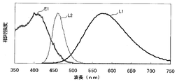
- FIG. 2 is a diagram showing excitation, emission spectrum of the first phosphor, and emission spectrum of the second phosphor.
- L1 is an emission spectrum indicating the wavelength range of light emitted from the first phosphor after wavelength conversion
- L2 is an emission spectrum indicating the wavelength range of light emitted by the second phosphor after wavelength conversion
- E1 is the first spectrum.
- the excitation spectrum which shows the excitation wavelength range which fluorescent substance wavelength-converts is shown. Since it is clear that the excitation spectrum of the second phosphor does not overlap with the emission spectrum of the first phosphor, the excitation spectrum of the second phosphor is not shown.
- the excitation spectrum E1 of the first phosphor hardly overlaps the emission spectrum L2 of the second phosphor. Further, as described above, the excitation spectrum of the second phosphor also does not overlap with the emission spectrum of the first phosphor. Therefore, the wavelength range of the light emitted by wavelength conversion between the first phosphor and the second phosphor is generally different from the mutual excitation wavelength range. For this reason, the blue light emitted after wavelength conversion by the second phosphor can pass through the light wavelength conversion member 16 with almost no absorption by the first phosphor. Further, yellow light that is wavelength-converted and emitted by the first phosphor can also pass through the light wavelength conversion member 16 with almost no absorption by the second phosphor.
- the thickness is not uniform, that is, the distance from the light emitting surface of the semiconductor light emitting element 14 to the light emitting surface of the light wavelength converting member 16 is not uniform. Even in this case, light can be emitted from the light wavelength conversion member 16 with a uniform color over the entire emission surface. Therefore, even when the light wavelength conversion member 16 is formed by a manufacturing method such as potting, a light emitting module that emits a uniform color can be manufactured.
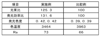
- FIG. 3 is a diagram illustrating values in the respective items of the light emitting module 10 according to the first embodiment and the light emitting module according to the comparative example.
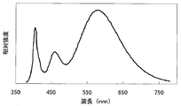
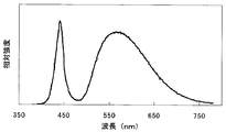
- FIG. 4 is a diagram showing an emission spectrum of the light emitting module 10 according to the first embodiment
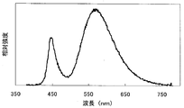
- FIG. 5 is a diagram showing an emission spectrum of the light emitting module of the comparative example.
- the light emission characteristics of the light emitting module of the comparative example were also examined.
- a comparative phosphor is used instead of the first phosphor and the second phosphor.
- this phosphor for comparison is blended in dimethyl silicone resin so as to be 0.7 vol%.
- cerium activated yttrium aluminum garnet P46-Y3 manufactured by Kasei Optonics
- the configuration of the light emitting module of the comparative example is the same as that of the light emitting module 10.
- each of the light emitting module 10 and the light emitting module of the comparative example was driven with a current of 700 mA, and the light emission characteristics were examined.
- each of the luminous flux ratio and the luminous efficiency ratio represents the ratio when the comparative example is 100.
- the light emitting module 10 according to the first embodiment has higher luminous flux and light emission efficiency and better color rendering than the light emitting module of the comparative example.
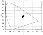
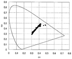
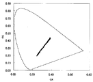
- FIG. 6 is a diagram illustrating a chromaticity distribution of emitted light by the light emitting module 10 according to the first embodiment.
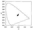
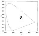
- FIG. 7 is a diagram illustrating a chromaticity distribution of emitted light by the light emitting module according to the comparative example.
- a Minolta CA1500 as a color luminance meter
- the chromaticity distribution obtained by dividing each potting surface of the light emitting module 10 and the light emitting module according to the comparative example by about 50 ⁇ m 2 was examined.
- the chromaticity distribution on the center line in the longitudinal direction of each light emitting module is plotted.
- the light emitting module 10 emits light with the same chromaticity in any part.
- the light-emitting module of the comparative example emits blue-colored white near the semiconductor light-emitting element 14 and changes to yellowish white as the distance from the semiconductor light-emitting element 14 increases. It can be seen that the variation is large.
- the color variation is further expanded, such as a bluish white portion and a yellowish white portion, depending on where the light is irradiated. This greatly impairs the quality of the lighting.
- the light emitting module 10 According to the light emitting module 10 according to the first embodiment, such a color variation can be suppressed, and the illuminated area can be illuminated with a uniform white color. Therefore, it turns out that the light emitting module 10 is especially useful for the use as a light source for illumination.
- the semiconductor light emitting element 14 is covered with the light wavelength conversion member 16 containing the first phosphor and the second phosphor whose wavelength range of light emitted by wavelength conversion is substantially different from the excitation wavelength of each other.
- the light wavelength conversion member 16 containing the first phosphor and the second phosphor whose wavelength range of light emitted by wavelength conversion is substantially different from the excitation wavelength of each other.
- FIG. 8 is a perspective view showing the configuration of the light emitting module 30 according to the second embodiment.
- the light emitting module 30 includes a case 32, a light emitting element unit 34, and a light wavelength conversion member 36.
- the case 32 is formed of a transparent polycarbonate and is formed in a rectangular parallelepiped box shape having a length of 45 mm, a width of 8 mm, a height of 5 mm, and a plate thickness of 0.2 mm, and only the upper surface is opened.
- the light emitting element unit 34 includes a support substrate 38 and a semiconductor light emitting element 40.
- the support substrate 38 is the same as the support substrate 12 according to the first embodiment in that a circuit is formed on the upper surface by aluminum vapor deposition and gold deposition.
- the support substrate 38 is formed in a rectangular plate shape having a length of 40 mm, a width of 5 mm, and a thickness of 1 mm.
- the semiconductor light emitting device 40 is the same as the semiconductor light emitting device 14 according to the first embodiment.
- five semiconductor light emitting elements 40 are arranged in series on the support substrate 38 to constitute the light emitting element unit 34.
- the interval between the semiconductor light emitting elements 40 is 5 mm.
- the light emitting element unit 34 was accommodated in the case 32 and fixed to the bottom surface.
- a power supply cord for supplying current to the light emitting element unit 34 was drawn out from the side surface of the case 32.
- the first phosphor and the second phosphor are mixed at a weight ratio of 2: 1, and the mixed phosphor is blended in a binder material made of dimethyl silicone resin so as to be 3.0 vol%. .
- the mixing method is the same as in the first embodiment.
- the phosphor paste was filled in a case 32 in which the light emitting element unit 34 was already fixed to the bottom using a 2.5 cc syringe (with a coating outlet diameter of 1 mm). After filling, the upper surface of the phosphor paste was flattened with a squeegee. Furthermore, the phosphor paste was cured by performing a heat treatment for maintaining the temperature at 150 ° C. for 1 hour, and the light wavelength conversion member 36 was formed.
- FIG. 9 is a diagram illustrating values in the respective items of the light emitting module 30 according to the second embodiment and the light emitting module according to the comparative example.
- FIG. 10 is a diagram illustrating an emission spectrum of the light emitting module 30 according to the second embodiment
- FIG. 11 is a diagram illustrating an emission spectrum of the light emitting module of the comparative example.
- a comparative phosphor is used instead of the first phosphor and the second phosphor.
- the material of the comparative phosphor is the same as that in the first embodiment.
- this phosphor for comparison is blended with dimethyl silicone resin so as to be 0.18 vol%.
- the configuration of the light emitting module of the comparative example is the same as that of the light emitting module 10.
- each of the light emitting module 30 and the light emitting module of the comparative example was driven with a current of 700 mA, and the light emission characteristics were examined.
- each of the luminous flux ratio and the luminous efficiency ratio represents a ratio when the comparative example is 100.
- the light emitting module 30 according to the second embodiment has higher luminous flux and light emission efficiency and better color rendering than the light emitting module of the comparative example.
- FIG. 12 is a diagram showing the detection location of the light emission chromaticity of the light emitting module 30 according to the first embodiment.
- the light emission chromaticity detection location of the light emitting module 30 is shown using a top view of the light emitting module 30.
- the light emission chromaticity of the light emitting module 30 was examined at a location corresponding to the second semiconductor light emitting element 40 from the end. Specifically, on the upper surface of the light wavelength conversion member 36, the vertical upper portion of the center of the semiconductor light emitting element 40 is the origin, the a axis passing through the origin and parallel to the extending direction of the support substrate 38, and the The light emission chromaticity was detected while moving the detection location on both the b-axis passing through the origin and perpendicular to the extending direction of the support substrate 38, and the chromaticity distribution was examined for each axis.
- CA 1500 manufactured by Minolta was used as a color luminance meter, and the chromaticity at 50 ⁇ m 2 on the upper surface of the light wavelength conversion member 36 was detected. The chromaticity was also detected at both the point B, which is the vertically upper portion of the center of the semiconductor light emitting element 40, and the point Y on the b-axis that is a predetermined distance (about 1 mm) from the point B. The same investigation as described above was performed for the light emitting module according to the comparative example.
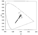
- FIG. 13 is a diagram illustrating the a-axis chromaticity distribution of the light emitting module 30 according to the second embodiment
- FIG. 14 is a diagram illustrating the a-axis chromaticity distribution of the light emitting module according to the comparative example
- 15 is a diagram illustrating the b-axis chromaticity distribution of the light-emitting module 30 according to the second embodiment
- FIG. 16 is a diagram illustrating the b-axis chromaticity distribution of the light-emitting module according to the comparative example. is there.
- the chromaticity does not change much even when the detection location is moved in both the a-axis and the b-axis.
- the chromaticity changes greatly when the detection position is moved in both the a-axis and the b-axis.
- the light emitting module according to the comparative example has a chromaticity variation from blue to yellow.
- the light emitting module emits blue white light immediately above the semiconductor light emitting element 40 and directly above the semiconductor light emitting element 40. It turns out that it changes to yellowish white by moving away from.
- FIG. 17 is a diagram showing the difference between the chromaticity at the point B and the chromaticity at the point Y for both the light emitting module 30 according to the second embodiment and the light emitting module according to the comparative example.
- the color difference between the B point and the Y point is 0.371, whereas in the light emitting module 30 according to the second embodiment, the color difference is reduced to 0.098, which is about a quarter. I understand.
- the semiconductor light emitting element 40 is covered by using the light wavelength conversion member 36 containing the first phosphor and the second phosphor whose wavelength range emitted by wavelength conversion is substantially different from the excitation wavelength of each other. By molding, a light emitting module with little color unevenness can be obtained.
- a plurality of semiconductor light emitting elements are scattered on a plane rather than in a straight line.
- the plurality of semiconductor light emitting elements are integrally covered by using a light wavelength conversion member containing a plurality of phosphors whose wavelength ranges emitted by wavelength conversion are different from the excitation wavelengths of each other. This makes it possible to obtain a light emitting module that emits light uniformly over a wide area on a plane.
- the light wavelength conversion member when the light wavelength conversion member is coated on the semiconductor light emitting element, the light wavelength conversion member is formed in a shape in which the distance from the light emitting surface of the light emitting element to the outer surface of the light wavelength conversion member is not uniform.
- the light wavelength conversion member may be formed in a cylindrical shape, a polygonal column shape, a conical shape, or a polygonal pyramid shape.
- a light wavelength conversion member containing a first phosphor, a second phosphor, and a third phosphor in which the wavelength range of light emitted by wavelength conversion is different from the excitation wavelength of each other is used.
- the light emitting module is provided by covering the semiconductor light emitting element.
- the first phosphor emits blue light by converting the wavelength of light emitted from the semiconductor light emitting element.
- the second phosphor emits green light by converting the wavelength of light emitted from the semiconductor light emitting element.
- the third phosphor emits red light by converting the wavelength of light emitted from the semiconductor light emitting element. According to this aspect as well, it is possible to provide a light emitting module that emits uniform white light by additive mixing of blue light, green light, and red light.
- a light emitting module is provided.
- the plurality of semiconductor light emitting elements are not the same, but are provided to emit light in a common wavelength range.
- Each of the plurality of phosphors is provided so as to convert the wavelength of light in the common wavelength range.
- the present invention can be used for a light-emitting module, and in particular, can be used for a light-emitting module including a light-emitting element and a light wavelength conversion member that converts the wavelength of light emitted from the light-emitting element and emits the light.
Landscapes
- Chemical & Material Sciences (AREA)
- Inorganic Chemistry (AREA)
- Engineering & Computer Science (AREA)
- Materials Engineering (AREA)
- Organic Chemistry (AREA)
- Led Device Packages (AREA)
- Luminescent Compositions (AREA)
Abstract
Description
図1は、第1の実施形態に係る発光モジュール10の構成を示す断面図である。発光モジュール10は、支持基板12、半導体発光素子14、および光波長変換部材16を有する。
支持基板12は窒化アルミニウム(AlN)によって形成され、金蒸着によって上面に回路が形成されている。なお、支持基板12は、例えば、アルミナ、ムライト、ガラスセラミックなどのセラミックや、ガラスエポキシなど、導電性を有しない一方、熱伝導性が高い他の材料によって形成されてもよい。第1の実施形態では、支持基板12は、長さ6mm、幅1mm、厚さ1mmの長方形プレート状に形成されている。
第1の実施形態では、半導体発光素子14として近紫外光または短波長可視光を発光するLEDを採用した。半導体発光素子14は、例えば1mm角のチップとして形成され、発する光の中心波長は約400nmとなるよう設けられている。第1の実施形態では、半導体発光素子14に、402nmにピーク波長を有するSemiLEDs社製のMvpLED(登録商標)SL-V-U40ACを用いた。なお、半導体発光素子14がこれに限られないことは勿論であり、例えば半導体レーザーダイオード(LD)が採用されてもよい。
光波長変換部材16は、複数の半導体発光素子14を一体的に被覆するよう形成される。光波長変換部材16は、波長変換して発する光の波長範囲が互いの励起波長と概ね異なる第1蛍光体および第2蛍光体を含有する。この第1蛍光体および第2蛍光体を透明なバインダーペーストに含有させて蛍光体ペーストを生成し、この蛍光体ペーストを複数の半導体発光素子14を一体的に被覆するようポッティングし硬化させることにより光波長変換部材16が形成される。
第1蛍光体は、近紫外光または短波長可視光を効率的に吸収する一方、450nm以上の可視光の吸収がほとんどないものを用いる。第1蛍光体は、近紫外光または短波長可視光を波長変換して黄色光を発する黄色蛍光体であり、放射する光のドミナント波長は564nm以上582nm以下のものを用いる。
第2蛍光体は、近紫外光または短波長可視光を波長変換して青色光を発する青色蛍光体である。第2蛍光体は、近紫外光または赤色光を効率的に吸収し、ドミナント波長が440nm以上470nm以下の光を放射するものを用いる。第1の実施形態では、第2蛍光体として、(Ca4.67Mg0.5)(PO4)3Cl:Eu0.08で表される蛍光体を用いた。なお、第2蛍光体はこれに限られず、以下の一般式で表される蛍光体群の中から選択してもよい。
M1はCa、Sr、Baのうち一種以上を必須とし、一部をMg、Zn,Cd、K、Ag、Tlからなる群の元素に置き換えることができる。M2は、Pを必須とし、一部をV、Si、As、Mn、Co、Cr、Mo、W、Bからなる群の元素に置き換えることができる。Xは少なくとも1種のハロゲン元素、ReはEu2+を必須とする少なくとも1種の希土類元素、またはMnを示す。また、aは4.2≦a≦5.8、bは2.5≦b≦3.5、cは0.8<c<1.4、dは0.01<d<0.1の範囲とされる。
M1は、Ca、Sr、Ba、Znからなる群より選ばれる少なくとも1種の元素、aは0.001≦a≦0.5の範囲とされる。
M1は、Ca、Sr、Ba、Znからなる群より選ばれる少なくとも1種の元素、aは0.001≦a≦0.8の範囲とされる。
M1は、Ca、Sr、Ba、Znからなる群より選ばれる少なくとも1種の元素、Xは少なくとも1種のハロゲン元素、aは0.001≦a≦0.5の範囲とされる。
バインダー材料は、近紫外光または短波長可視光に対して透明、すなわちこれらの光の透過率が90%以上であり、光耐性が良好な材料を用いる。第1の実施形態では、バインダー材料としてシリコーン樹脂を用いた。具体的には、バインダー材料として、耐光性の良好なジメチルシリコーン樹脂(東レ・ダウコーニング製JCR6126)を用いた。しかしバインダー材料はこれに限られず、例えばフッ素樹脂、ゾルゲルガラス、アクリル樹脂、無機バインダー、ガラス材料等を用いることができる。
発光モジュール10を製造するにあたって、まず、予め金蒸着によって陽極および陰極を含む電極パターンを支持基板12に形成した。次に、ディスペンサーを用いて銀ペースト(エイブルスティック社製:84-1LMISR4)を支持基板12の陽極上に滴下し、その上に2個の半導体発光素子14の各々の下面(被支持面)を接着した。こうして銀ペーストを175℃環境下で1時間硬化させた。その後、ワイヤとしてφ45μmの金ワイヤを、半導体発光素子14の上面側電極および支持基板12の陰極にそれぞれ超音波熱圧着にて接合した。
図8は、第2の実施形態に係る発光モジュール30の構成を示す斜視図である。発光モジュール30は、ケース32、発光素子ユニット34、および光波長変換部材36を有する。
Claims (10)
- 発光素子と、
前記発光素子が発する光を波長変換して出射する光波長変換部材と、
を備え、
前記光波長変換部材は、波長変換して発する光の波長範囲が互いの励起波長と異なる複数の蛍光体を含有し、前記発光素子を被覆するよう形成されることを特徴とする発光モジュール。 - 前記発光素子は、互いに離間して複数並設され、
光波長変換部材は、前記複数の発光素子を一体的に被覆するよう形成されることを特徴とする請求項1に記載の発光モジュール。 - 前記複数の発光素子は、同一平面上に配置されることを特徴とする請求項2に記載の発光モジュール。
- 前記複数の発光素子は、一直線上に並設されることを特徴とする請求項2または3に記載の発光モジュール。
- 前記複数の発光素子は、平面上に散在するよう配置されることを特徴とする請求項2または3に記載の発光モジュール。
- 近紫外または短波長可視の波長範囲の光を発する発光素子と、
一般式がM1O2・a(M2 1-z,M4 z)O・bM3X2(但し、M1はSi、Ge、Ti、Zr及びSnからなる群より選ばれる少なくとも1種の元素、M2はMg、Ca、Sr、Ba及びZnからなる群より選ばれる少なくとも1種の元素、M3はMg、Ca、Sr、Ba及びZnからなる群より選ばれる少なくとも1種の元素、Xは少なくとも1種のハロゲン元素、M4は希土類元素及びMnからなる群より選ばれるEu2+を必須とする少なくとも1種の元素を示す。aは0.1≦a≦1.3、bは0.1≦b≦0.25、zは0.03<z<0.8の範囲である。)で表される第1蛍光体と、前記発光素子が発する光を波長変換して青色光を発する第2蛍光体と、の双方を含有し、前記発光素子を被覆するよう形成される光波長変換部材と、
を備えることを特徴とする発光モジュール。 - 前記発光素子は、互いに離間して複数並設され、
光波長変換部材は、前記複数の発光素子を一体的に被覆するよう形成されることを特徴とする請求項1に記載の発光モジュール。 - 前記複数の発光素子は、同一平面上に配置されることを特徴とする請求項5に記載の発光モジュール。
- 前記複数の発光素子は、一直線上に並設されることを特徴とする請求項7または8に記載の発光モジュール。
- 前記複数の発光素子は、平面上に散在するよう配置されることを特徴とする請求項7または8に記載の発光モジュール。
Priority Applications (4)
| Application Number | Priority Date | Filing Date | Title |
|---|---|---|---|
| JP2011519505A JPWO2010150459A1 (ja) | 2009-06-23 | 2010-05-24 | 発光モジュール |
| EP10791785.8A EP2448020A4 (en) | 2009-06-23 | 2010-05-24 | LIGHT-EMITTING MODULE |
| US13/380,390 US20120092853A1 (en) | 2009-06-23 | 2010-05-24 | Light emitting module |
| CN2010800280568A CN102804420A (zh) | 2009-06-23 | 2010-05-24 | 发光模块 |
Applications Claiming Priority (2)
| Application Number | Priority Date | Filing Date | Title |
|---|---|---|---|
| JP2009-149112 | 2009-06-23 | ||
| JP2009149112 | 2009-06-23 |
Publications (1)
| Publication Number | Publication Date |
|---|---|
| WO2010150459A1 true WO2010150459A1 (ja) | 2010-12-29 |
Family
ID=43386249
Family Applications (1)
| Application Number | Title | Priority Date | Filing Date |
|---|---|---|---|
| PCT/JP2010/003462 Ceased WO2010150459A1 (ja) | 2009-06-23 | 2010-05-24 | 発光モジュール |
Country Status (6)
| Country | Link |
|---|---|
| US (1) | US20120092853A1 (ja) |
| EP (1) | EP2448020A4 (ja) |
| JP (2) | JPWO2010150459A1 (ja) |
| KR (1) | KR20120024976A (ja) |
| CN (1) | CN102804420A (ja) |
| WO (1) | WO2010150459A1 (ja) |
Cited By (2)
| Publication number | Priority date | Publication date | Assignee | Title |
|---|---|---|---|---|
| JP2013033938A (ja) * | 2011-06-28 | 2013-02-14 | Koito Mfg Co Ltd | 発光モジュール |
| US9333905B2 (en) | 2013-01-30 | 2016-05-10 | Koito Manufacturing Co., Ltd. | Light emitting module |
Families Citing this family (5)
| Publication number | Priority date | Publication date | Assignee | Title |
|---|---|---|---|---|
| JP6056213B2 (ja) * | 2012-06-26 | 2017-01-11 | 東芝ライテック株式会社 | 発光モジュール及び照明装置 |
| US9761763B2 (en) * | 2012-12-21 | 2017-09-12 | Soraa, Inc. | Dense-luminescent-materials-coated violet LEDs |
| JP2016058614A (ja) * | 2014-09-11 | 2016-04-21 | パナソニックIpマネジメント株式会社 | 発光装置、及び照明装置 |
| DE102015107580A1 (de) * | 2015-05-13 | 2016-11-17 | Osram Opto Semiconductors Gmbh | Strahlungsemittierendes optoelektronisches Bauelement |
| CN110630976A (zh) * | 2018-06-22 | 2019-12-31 | 株式会社小糸制作所 | 发光模块 |
Citations (9)
| Publication number | Priority date | Publication date | Assignee | Title |
|---|---|---|---|---|
| JPH10107325A (ja) | 1996-09-30 | 1998-04-24 | Nichia Chem Ind Ltd | 発光装置及びそれを用いた表示装置 |
| JPH1146019A (ja) | 1997-07-28 | 1999-02-16 | Nichia Chem Ind Ltd | 発光ダイオード及びled表示器の形成方法 |
| JP2002185048A (ja) | 2000-10-13 | 2002-06-28 | Lumileds Lighting Us Llc | 発光ダイオードのステンシル蛍光体層 |
| JP2003031011A (ja) * | 2001-07-16 | 2003-01-31 | Stanley Electric Co Ltd | 灯具用線状光源 |
| JP2004247150A (ja) * | 2003-02-13 | 2004-09-02 | Koito Mfg Co Ltd | 車両用前照灯 |
| JP2004247151A (ja) * | 2003-02-13 | 2004-09-02 | Koito Mfg Co Ltd | 車両用前照灯 |
| JP2008274240A (ja) * | 2007-04-05 | 2008-11-13 | Koito Mfg Co Ltd | 蛍光体 |
| JP2009009898A (ja) * | 2007-06-29 | 2009-01-15 | Toshiba Lighting & Technology Corp | 照明装置および照明器具 |
| JP2009038348A (ja) * | 2007-07-12 | 2009-02-19 | Koito Mfg Co Ltd | 発光装置 |
Family Cites Families (15)
| Publication number | Priority date | Publication date | Assignee | Title |
|---|---|---|---|---|
| JP2002344029A (ja) * | 2001-05-17 | 2002-11-29 | Rohm Co Ltd | 発光ダイオードの色調調整方法 |
| JP2004127988A (ja) * | 2002-09-30 | 2004-04-22 | Toyoda Gosei Co Ltd | 白色発光装置 |
| US20040183081A1 (en) * | 2003-03-20 | 2004-09-23 | Alexander Shishov | Light emitting diode package with self dosing feature and methods of forming same |
| US7005679B2 (en) * | 2003-05-01 | 2006-02-28 | Cree, Inc. | Multiple component solid state white light |
| EP1753840B1 (en) * | 2004-05-27 | 2008-05-14 | Philips Intellectual Property & Standards GmbH | Illumination system comprising a radiation source and a fluorescent material |
| WO2006111906A2 (en) * | 2005-04-19 | 2006-10-26 | Philips Intellectual Property & Standards Gmbh | Illumination system comprising a red-emitting ceramic luminescence converter |
| JP2006332134A (ja) * | 2005-05-23 | 2006-12-07 | Ijin Jo | 白色発光ダイオード |
| JP2007088095A (ja) * | 2005-09-20 | 2007-04-05 | Matsushita Electric Works Ltd | 発光装置 |
| JP2007103512A (ja) * | 2005-09-30 | 2007-04-19 | Kyocera Corp | 発光装置 |
| JP4838005B2 (ja) * | 2006-02-20 | 2011-12-14 | 京セラ株式会社 | 発光装置 |
| KR101258227B1 (ko) * | 2006-08-29 | 2013-04-25 | 서울반도체 주식회사 | 발광 소자 |
| JP2008244468A (ja) * | 2007-02-28 | 2008-10-09 | Toshiba Lighting & Technology Corp | 発光装置 |
| EP2015614B1 (en) * | 2007-07-12 | 2010-12-15 | Koito Manufacturing Co., Ltd. | Light emitting device |
| JP2009111273A (ja) * | 2007-10-31 | 2009-05-21 | Toshiba Lighting & Technology Corp | 発光装置 |
| US8461613B2 (en) * | 2008-05-27 | 2013-06-11 | Interlight Optotech Corporation | Light emitting device |
-
2010
- 2010-05-24 US US13/380,390 patent/US20120092853A1/en not_active Abandoned
- 2010-05-24 KR KR1020127001286A patent/KR20120024976A/ko not_active Ceased
- 2010-05-24 EP EP10791785.8A patent/EP2448020A4/en not_active Withdrawn
- 2010-05-24 CN CN2010800280568A patent/CN102804420A/zh active Pending
- 2010-05-24 JP JP2011519505A patent/JPWO2010150459A1/ja active Pending
- 2010-05-24 WO PCT/JP2010/003462 patent/WO2010150459A1/ja not_active Ceased
-
2014
- 2014-01-29 JP JP2014013970A patent/JP5852149B2/ja not_active Expired - Fee Related
Patent Citations (9)
| Publication number | Priority date | Publication date | Assignee | Title |
|---|---|---|---|---|
| JPH10107325A (ja) | 1996-09-30 | 1998-04-24 | Nichia Chem Ind Ltd | 発光装置及びそれを用いた表示装置 |
| JPH1146019A (ja) | 1997-07-28 | 1999-02-16 | Nichia Chem Ind Ltd | 発光ダイオード及びled表示器の形成方法 |
| JP2002185048A (ja) | 2000-10-13 | 2002-06-28 | Lumileds Lighting Us Llc | 発光ダイオードのステンシル蛍光体層 |
| JP2003031011A (ja) * | 2001-07-16 | 2003-01-31 | Stanley Electric Co Ltd | 灯具用線状光源 |
| JP2004247150A (ja) * | 2003-02-13 | 2004-09-02 | Koito Mfg Co Ltd | 車両用前照灯 |
| JP2004247151A (ja) * | 2003-02-13 | 2004-09-02 | Koito Mfg Co Ltd | 車両用前照灯 |
| JP2008274240A (ja) * | 2007-04-05 | 2008-11-13 | Koito Mfg Co Ltd | 蛍光体 |
| JP2009009898A (ja) * | 2007-06-29 | 2009-01-15 | Toshiba Lighting & Technology Corp | 照明装置および照明器具 |
| JP2009038348A (ja) * | 2007-07-12 | 2009-02-19 | Koito Mfg Co Ltd | 発光装置 |
Non-Patent Citations (1)
| Title |
|---|
| See also references of EP2448020A4 |
Cited By (3)
| Publication number | Priority date | Publication date | Assignee | Title |
|---|---|---|---|---|
| JP2013033938A (ja) * | 2011-06-28 | 2013-02-14 | Koito Mfg Co Ltd | 発光モジュール |
| US9333905B2 (en) | 2013-01-30 | 2016-05-10 | Koito Manufacturing Co., Ltd. | Light emitting module |
| KR20160083839A (ko) | 2013-01-30 | 2016-07-12 | 가부시키가이샤 고이토 세이사꾸쇼 | 발광 모듈 |
Also Published As
| Publication number | Publication date |
|---|---|
| US20120092853A1 (en) | 2012-04-19 |
| KR20120024976A (ko) | 2012-03-14 |
| JP2014082527A (ja) | 2014-05-08 |
| CN102804420A (zh) | 2012-11-28 |
| EP2448020A1 (en) | 2012-05-02 |
| JPWO2010150459A1 (ja) | 2012-12-06 |
| JP5852149B2 (ja) | 2016-02-03 |
| EP2448020A4 (en) | 2014-04-30 |
Similar Documents
| Publication | Publication Date | Title |
|---|---|---|
| JP5852149B2 (ja) | 発光モジュール | |
| JP5468985B2 (ja) | 照明装置 | |
| JP5752650B2 (ja) | 発光装置 | |
| CN101288342B (zh) | 包括陶瓷发光转换器的照明系统 | |
| JP5076017B2 (ja) | 発光装置 | |
| JP5740344B2 (ja) | 発光装置の製造方法 | |
| JP5677377B2 (ja) | 発光装置 | |
| JP2011181793A (ja) | 発光装置 | |
| CN103113883B (zh) | 发光材料 | |
| JP5319743B2 (ja) | 発光装置 | |
| JP2010129906A (ja) | 表示装置用照明装置及び表示装置 | |
| JPWO2006077740A1 (ja) | 発光装置及びその製造方法 | |
| US20090020775A1 (en) | RED LINE EMITTING COMPLEX FLUORIDE PHOSPHORS ACTIVATED WITH Mn4+ | |
| JP2011071404A (ja) | 発光装置および照明装置 | |
| JP2004115633A (ja) | 珪酸塩蛍光体およびそれを用いた発光装置 | |
| JP4929413B2 (ja) | 発光装置 | |
| JP2010225960A (ja) | 発光装置および照明装置 | |
| JP5566263B2 (ja) | 発光モジュール | |
| JP2011155125A (ja) | 発光装置および照明装置 | |
| JP6231787B2 (ja) | 蛍光体及び発光装置 | |
| JP5462211B2 (ja) | 白色発光装置 | |
| JP2010199273A (ja) | 発光装置および照明装置 | |
| JP5194395B2 (ja) | 酸窒化物系蛍光体及びこれを用いた発光装置 | |
| JP4948015B2 (ja) | アルミン酸系青色蛍光体およびそれを用いた発光装置 | |
| CN114497323A (zh) | 波长转换结构、具有波长转换结构的发光装置及显示装置 |
Legal Events
| Date | Code | Title | Description |
|---|---|---|---|
| WWE | Wipo information: entry into national phase |
Ref document number: 201080028056.8 Country of ref document: CN |
|
| 121 | Ep: the epo has been informed by wipo that ep was designated in this application |
Ref document number: 10791785 Country of ref document: EP Kind code of ref document: A1 |
|
| WWE | Wipo information: entry into national phase |
Ref document number: 2011519505 Country of ref document: JP |
|
| WWE | Wipo information: entry into national phase |
Ref document number: 13380390 Country of ref document: US Ref document number: 2010791785 Country of ref document: EP |
|
| NENP | Non-entry into the national phase |
Ref country code: DE |
|
| ENP | Entry into the national phase |
Ref document number: 20127001286 Country of ref document: KR Kind code of ref document: A |