WO2011004869A1 - 置換ベンゾカルコゲノアセン化合物、該化合物を含有する薄膜及び該薄膜を含有する有機半導体デバイス - Google Patents
置換ベンゾカルコゲノアセン化合物、該化合物を含有する薄膜及び該薄膜を含有する有機半導体デバイス Download PDFInfo
- Publication number
- WO2011004869A1 WO2011004869A1 PCT/JP2010/061634 JP2010061634W WO2011004869A1 WO 2011004869 A1 WO2011004869 A1 WO 2011004869A1 JP 2010061634 W JP2010061634 W JP 2010061634W WO 2011004869 A1 WO2011004869 A1 WO 2011004869A1
- Authority
- WO
- WIPO (PCT)
- Prior art keywords
- group
- carbon atoms
- formula
- compound
- bond
- Prior art date
- Legal status (The legal status is an assumption and is not a legal conclusion. Google has not performed a legal analysis and makes no representation as to the accuracy of the status listed.)
- Ceased
Links
- 0 *1c([s]cc2)c2S=C1 Chemical compound *1c([s]cc2)c2S=C1 0.000 description 5
- WIPLFFSIOOLSMN-UHFFFAOYSA-N c(cc1)cc2c1[nH]c1c2[nH]c2c1[nH]c1ccccc21 Chemical compound c(cc1)cc2c1[nH]c1c2[nH]c2c1[nH]c1ccccc21 WIPLFFSIOOLSMN-UHFFFAOYSA-N 0.000 description 2
- SXPRVMIZFRCAGC-UHFFFAOYSA-N Cc(c(F)c(c(F)c1F)F)c1F Chemical compound Cc(c(F)c(c(F)c1F)F)c1F SXPRVMIZFRCAGC-UHFFFAOYSA-N 0.000 description 1
- RAUFSQCDQBYVRW-UHFFFAOYSA-N Cc1cc([o]cc2)c2[s]1 Chemical compound Cc1cc([o]cc2)c2[s]1 RAUFSQCDQBYVRW-UHFFFAOYSA-N 0.000 description 1
- BLZKSRBAQDZAIX-UHFFFAOYSA-N Cc1cc(cccc2)c2[s]1 Chemical compound Cc1cc(cccc2)c2[s]1 BLZKSRBAQDZAIX-UHFFFAOYSA-N 0.000 description 1
- WACNXHCZHTVBJM-UHFFFAOYSA-N Fc(cc(c(F)c1F)F)c1F Chemical compound Fc(cc(c(F)c1F)F)c1F WACNXHCZHTVBJM-UHFFFAOYSA-N 0.000 description 1
Images

Classifications
-
- C—CHEMISTRY; METALLURGY
- C07—ORGANIC CHEMISTRY
- C07D—HETEROCYCLIC COMPOUNDS
- C07D495/00—Heterocyclic compounds containing in the condensed system at least one hetero ring having sulfur atoms as the only ring hetero atoms
- C07D495/12—Heterocyclic compounds containing in the condensed system at least one hetero ring having sulfur atoms as the only ring hetero atoms in which the condensed system contains three hetero rings
- C07D495/14—Ortho-condensed systems
-
- C—CHEMISTRY; METALLURGY
- C07—ORGANIC CHEMISTRY
- C07D—HETEROCYCLIC COMPOUNDS
- C07D495/00—Heterocyclic compounds containing in the condensed system at least one hetero ring having sulfur atoms as the only ring hetero atoms
- C07D495/02—Heterocyclic compounds containing in the condensed system at least one hetero ring having sulfur atoms as the only ring hetero atoms in which the condensed system contains two hetero rings
- C07D495/04—Ortho-condensed systems
-
- C—CHEMISTRY; METALLURGY
- C07—ORGANIC CHEMISTRY
- C07F—ACYCLIC, CARBOCYCLIC OR HETEROCYCLIC COMPOUNDS CONTAINING ELEMENTS OTHER THAN CARBON, HYDROGEN, HALOGEN, OXYGEN, NITROGEN, SULFUR, SELENIUM OR TELLURIUM
- C07F7/00—Compounds containing elements of Groups 4 or 14 of the Periodic Table
- C07F7/02—Silicon compounds
- C07F7/08—Compounds having one or more C—Si linkages
- C07F7/0803—Compounds with Si-C or Si-Si linkages
- C07F7/081—Compounds with Si-C or Si-Si linkages comprising at least one atom selected from the elements N, O, halogen, S, Se or Te
- C07F7/0812—Compounds with Si-C or Si-Si linkages comprising at least one atom selected from the elements N, O, halogen, S, Se or Te comprising a heterocyclic ring
- C07F7/0814—Compounds with Si-C or Si-Si linkages comprising at least one atom selected from the elements N, O, halogen, S, Se or Te comprising a heterocyclic ring said ring is substituted at a C ring atom by Si
-
- H—ELECTRICITY
- H10—SEMICONDUCTOR DEVICES; ELECTRIC SOLID-STATE DEVICES NOT OTHERWISE PROVIDED FOR
- H10K—ORGANIC ELECTRIC SOLID-STATE DEVICES
- H10K10/00—Organic devices specially adapted for rectifying, amplifying, oscillating or switching; Organic capacitors or resistors having potential barriers
- H10K10/40—Organic transistors
- H10K10/46—Field-effect transistors, e.g. organic thin-film transistors [OTFT]
- H10K10/462—Insulated gate field-effect transistors [IGFETs]
- H10K10/484—Insulated gate field-effect transistors [IGFETs] characterised by the channel regions
-
- H—ELECTRICITY
- H10—SEMICONDUCTOR DEVICES; ELECTRIC SOLID-STATE DEVICES NOT OTHERWISE PROVIDED FOR
- H10K—ORGANIC ELECTRIC SOLID-STATE DEVICES
- H10K85/00—Organic materials used in the body or electrodes of devices covered by this subclass
- H10K85/40—Organosilicon compounds, e.g. TIPS pentacene
-
- H—ELECTRICITY
- H10—SEMICONDUCTOR DEVICES; ELECTRIC SOLID-STATE DEVICES NOT OTHERWISE PROVIDED FOR
- H10K—ORGANIC ELECTRIC SOLID-STATE DEVICES
- H10K85/00—Organic materials used in the body or electrodes of devices covered by this subclass
- H10K85/60—Organic compounds having low molecular weight
- H10K85/649—Aromatic compounds comprising a hetero atom
- H10K85/657—Polycyclic condensed heteroaromatic hydrocarbons
- H10K85/6576—Polycyclic condensed heteroaromatic hydrocarbons comprising only sulfur in the heteroaromatic polycondensed ring system, e.g. benzothiophene
-
- H—ELECTRICITY
- H10—SEMICONDUCTOR DEVICES; ELECTRIC SOLID-STATE DEVICES NOT OTHERWISE PROVIDED FOR
- H10K—ORGANIC ELECTRIC SOLID-STATE DEVICES
- H10K10/00—Organic devices specially adapted for rectifying, amplifying, oscillating or switching; Organic capacitors or resistors having potential barriers
- H10K10/40—Organic transistors
- H10K10/46—Field-effect transistors, e.g. organic thin-film transistors [OTFT]
- H10K10/462—Insulated gate field-effect transistors [IGFETs]
- H10K10/466—Lateral bottom-gate IGFETs comprising only a single gate
Definitions
- the present invention relates to a substituted benzochalcogenoacene compound, a thin film containing the compound, an organic semiconductor device having the thin film, and the like.
- Non-patent document 1 describes dibenzo [d, d ′] thieno [3,2-b; 4,5′-b ′] dithiophene as a compound that can be used as an organic semiconductor material.
- Benzochalcogenoacene compounds represented by the following formula are described.
- each E independently represents a sulfur or selenium atom.
- R 1 and R 2 each independently represent a hydrogen atom, an optionally substituted alkyl group having 4 to 30 carbon atoms, or a substituted group.
- An aralkyl group, a heteroaryl group having 4 to 30 carbon atoms which may have a substituent, a heteroaralkyl group having 5 to 30 carbon atoms which may have a substituent, and a fluorine atom Represents a trialkylsilyl group having 3 to 30 carbon atoms, provided that R 1 and R 2 are not hydrogen atoms at the same time.
- R 1 and R 2 in Formula (1) are each independently a hydrogen atom, an alkyl group having 4 to 30 carbon atoms which may have a fluorine atom, or an optionally substituted carbon atom.
- each E independently represents a sulfur or selenium atom.
- R 1 and R 2 are each independently a hydrogen atom, an alkyl group having 4 to 30 carbon atoms which may have a fluorine atom as a substituent, or a carbon atom having 3 to 3 carbon atoms which may have a fluorine atom as a substituent.
- ⁇ 24> A thin film containing the compound according to any one of ⁇ 1> to ⁇ 23>; ⁇ 25> A thin film comprising the compound according to any one of ⁇ 1> to ⁇ 23>; ⁇ 26> An organic semiconductor device containing the thin film according to ⁇ 24> or ⁇ 25>; ⁇ 27> An organic transistor containing the thin film according to ⁇ 24> or ⁇ 25>; Etc.
- the present invention can provide a novel substituted benzochalcogenoacene compound.
- substituted benzochalcogenoacene compound (1) the substituted benzochalcogenoacene compound represented by the above formula (1) of the present invention (hereinafter sometimes referred to as “substituted benzochalcogenoacene compound (1)”) will be described in detail.
- E independently represents a sulfur or selenium atom.
- R 1 and R 2 are each independently a hydrogen atom, an optionally substituted alkyl group having 4 to 30 carbon atoms, an optionally substituted alkoxy group having 4 to 30 carbon atoms, An aryl group having 6 to 30 carbon atoms which may have a substituent, an aralkyl group having 7 to 30 carbon atoms which may have a substituent, and 4 to 30 carbon atoms which may have a substituent.
- at least one of R 1 and R 2 is not a hydrogen atom.
- alkyl group having 4 to 30 carbon atoms of the “alkyl group having 4 to 30 carbon atoms which may have a substituent” in R 1 and R 2 may be any of linear, branched, and cyclic Good.
- Specific examples of the alkyl group having 4 to 30 carbon atoms include n-butyl, s-butyl, t-butyl, n-pentyl, neopentyl, n-hexyl, 2-ethylhexyl, and n-heptyl.
- n-octyl group 2-hexyloctyl group, n-nonyl group, n-decyl group, 2-hexyldecyl group, n-undecyl group, n-dodecyl group, n-tridecyl group, n-tetradecyl group, n -Pentadecyl, n-hexadecyl, n-heptadecyl, n-octadecyl, n-nonadecyl, n-icosyl, n-henicosyl, n-docosyl, n-tricosyl, n-tetracosyl, n -Pentacosyl group, n-hexacosyl group, n-heptacosyl group, n-octacosyl group, n-nonacosyl group, n-triacontyl group, cyclopen
- Examples of the substituent of the alkyl group having 4 to 30 carbon atoms include a halogen atom and an alkoxy group having 1 to 30 carbon atoms.
- Examples of the halogen atom include a fluorine atom, a chlorine atom, and a bromine atom.
- Examples of the alkoxy group having 1 to 30 carbon atoms include methoxy group, ethoxy group, n-propoxy group, n-butoxy group, n-pentyloxy group, n-hexyloxy group, n-heptyloxy group, and n-octyloxy group.
- N-nonyloxy group N-nonyloxy group, n-decyloxy group, n-undecyloxy group, n-dodecyloxy group, n-tridecyloxy group, n-tetradecyloxy group, n-pentadecyloxy group, n-hexadecyloxy group Group, n-heptadecyloxy group, n-octadecyloxy group, n-nonadecyloxy group, n-icosyloxy group, n-henicosyloxy group, n-docosyloxy group, n-tricosyloxy group, n-tetracosyl group Oxy group, n-pentacosyloxy group, n-hexacosyloxy group, n-heptacosyloxy group, n-octacosyloxy group Group, n- Nonakoshiruokishi group, such as n
- the substituent that the alkyl group having 4 to 30 carbon atoms has is preferably a fluorine atom.
- Examples of the alkyl group having 4 to 30 carbon atoms having a fluorine atom include a perfluorohexyl group, a perfluorooctyl group, a perfluorodecyl group, a perfluorododecyl group, and a perfluorotridecyl group.
- alkoxy group having 4 to 30 carbon atoms examples include, for example, an n-butoxy group, n-pentyloxy, and the like.
- Examples of the substituent of the “optionally substituted alkoxy group having 4 to 30 carbon atoms” include halogen atoms such as fluorine atom, chlorine atom and bromine atom, alkoxy group having 1 to 30 carbon atoms, carbon Examples thereof include an aryl group having 6 to 30 carbon atoms, an aralkyl group having 7 to 30 carbon atoms, a heteroaryl group having 4 to 30 carbon atoms, and a heteroaralkyl group having 5 to 30 carbon atoms.
- the hydrogen atom contained in the substituent may be replaced with a fluorine atom.
- Examples of the aryl group include a phenyl group, a 1-naphthyl group, and a 2-naphthyl group.
- aralkyl group examples include a group represented by the following formula.
- n1 represents 1 to 24, and n2 and n3 represent 1 to 20.
- the heteroaryl group means a group in which at least one of the carbon atoms contained in the aromatic ring of the aryl group is replaced by a hetero atom such as a nitrogen atom, an oxygen atom, a sulfur atom, or a selenium atom.
- a thienyl group, Furyl group, thiazolyl group, thieno [3,2-b] thienyl group, fluoro [3,2-b] furyl group, thieno [3,2-b] furyl group, benzo [b] thienyl group, benzo [b] A furyl group etc. are mentioned.
- a thienyl group, a thiazolyl group, a thieno [3,2-b] thienyl group, a benzo [b] thienyl group, and a benzo [b] furyl group are preferable.
- the heteroaralkyl group means a group in which at least one carbon atom contained in the aromatic ring of the aralkyl group is replaced by a heteroatom such as a nitrogen atom, an oxygen atom, a sulfur atom, or a selenium atom.
- a heteroatom such as a nitrogen atom, an oxygen atom, a sulfur atom, or a selenium atom.
- Examples include groups represented by the following formula.
- n4 represents 1 to 26
- n5 represents 1 to 24, and n6 represents 1 to 22. More preferably, a following formula can be mentioned.
- n4 represents 1 to 26, n5 represents 1 to 24, and n6 represents 1 to 22.
- the substituent that the alkoxy group having 4 to 30 carbon atoms has is preferably a fluorine atom.
- Examples of the alkoxy group having 4 to 30 carbon atoms having a substituent include perfluorohexyloxy group, perfluorooctyloxy group, perfluorodecyloxy group, perfluorododecyloxy group, perfluorotridecyloxy group, methoxy An ethoxyethoxy group etc. are mentioned.
- the “aryl group” in the “optionally substituted aryl group having 6 to 30 carbon atoms” in R 1 and R 2 is preferably monocyclic or bicyclic, more preferably a phenyl group, Examples include 1-naphthyl group and 2-naphthyl group.
- Examples of the substituent of the “aryl group which may have a substituent” include, for example, a halogen atom such as a fluorine atom, a chlorine atom and a bromine atom, for example, an alkyl group having 1 to 30 carbon atoms, and 1 to 30 carbon atoms. And an alkoxy group having 6 to 30 carbon atoms, an aralkyl group having 7 to 30 carbon atoms, a heteroaryl group having 4 to 30 carbon atoms, and a heteroaralkyl group having 5 to 30 carbon atoms.
- the hydrogen atom contained in the substituent may be replaced with a fluorine atom.
- aryl group optionally having a substituent examples include a phenyl group, a 1-naphthyl group, a 2-naphthyl group, a perfluorophenyl group, a 4-hexylphenyl group, a 4-hexyloxyphenyl group, and the like. Can be mentioned.
- alkyl group having 1 to 30 carbon atoms examples include methyl group, ethyl group, n-propyl group, n-butyl group, n-pentyl group, n-hexyl group, n-heptyl group, n-octyl group, n -Nonyl group, n-decyl group, n-undecyl group, n-dodecyl group, n-tridecyl group, n-tetradecyl group, n-pentadecyl group, n-hexadecyl group, n-heptadecyl group, n-octadecyl group, n -Nonadecyl group, n-icosyl group, n-henicosyl group, n-docosyl group, n-tricosyl group, n-tetracosyl group, n-pentacosyl
- Examples of the substituent of the “optionally substituted aralkyl group having 7 to 30 carbon atoms” in R 1 and R 2 include halogen atoms such as fluorine atom, chlorine atom, bromine atom, Examples thereof include an alkyl group having 1 to 30 carbon atoms, an alkoxy group having 1 to 30 carbon atoms, an aralkyl group having 7 to 30 carbon atoms, a heteroaryl group having 4 to 30 carbon atoms, and a heteroaralkyl group having 5 to 30 carbon atoms. .
- the hydrogen atom contained in the substituent alkyl group, alkoxy group, aralkyl group, heteroaryl group or heteroaralkyl group may be replaced by a fluorine atom.
- the substituent of the “optionally substituted aralkyl group having 7 to 30 carbon atoms” is preferably a fluorine atom.
- the “optionally substituted aralkyl group having 7 to 30 carbon atoms” for example, the following formula (Wherein n1 represents 1 to 24, n2 and n3 represent 1 to 20), an aralkyl group having 7 to 30 carbon atoms, Following formula (Wherein n4 and n5 represent 1 to 24, and n6 represents 1 to 23), and an aralkyl group having a substituent having 7 to 30 carbon atoms.
- Examples of the “optionally substituted heteroaryl group having 4 to 30 carbon atoms” in R 1 and R 2 include, for example, a thienyl group, a furyl group, a thiazolyl group, a thieno [3,2-b] thienyl group. Fluoro [3,2-b] furyl group, thieno [3,2-b] furyl group, benzo [b] thienyl group, benzo [b] furyl group and the like.
- heteroaryl group a thienyl group, a thiazolyl group, a thieno [3,2-b] thienyl group, a benzo [b] thienyl group, a benzo [b] furyl group, more preferably The group shown by these is mentioned.
- Examples of the substituent of the “heteroaryl group which may have a substituent” include, for example, a halogen atom such as a fluorine atom, a chlorine atom and a bromine atom, for example, an alkyl group having 1 to 30 carbon atoms, Examples include 30 alkoxy groups, aryl groups having 6 to 30 carbon atoms, aralkyl groups having 7 to 30 carbon atoms, heteroaryl groups having 4 to 30 carbon atoms, and heteroaralkyl groups having 5 to 30 carbon atoms.
- the hydrogen atom contained in the substituent may be replaced with a fluorine atom.
- Examples of the “optionally substituted heteroaryl group” include 2-thienyl group, 2-thieno [3,2-b] thienyl group, 2-benzo [b] thienyl group, 5-fluoro-2- Examples include thienyl group, 5-hexyl-2-thienyl group, 4-hexyloxy-2-thienyl group, and the like.
- substituent of the “optionally substituted heteroaralkyl group having 5 to 30 carbon atoms” include, for example, a halogen atom such as a fluorine atom, a chlorine atom and a bromine atom, such as an alkyl having 1 to 30 carbon atoms.
- a halogen atom such as a fluorine atom, a chlorine atom and a bromine atom
- alkyl having 1 to 30 carbon atoms such as an alkyl having 1 to 30 carbon atoms.
- the hydrogen atom contained in the substituent may be replaced with a fluorine atom.
- n4 represents 1 to 26
- n5 represents 1 to 24
- n6 represents 1 to 22.
- the trialkylsilyl group in the “trialkylsilyl group having 3 to 30 carbon atoms which may have a fluorine atom” in R 1 and R 2 is the number of carbon atoms of the three alkyl groups bonded to the silicon atom.
- the maximum number of carbon atoms of one alkyl group bonded to a silicon atom is 28, and this is an alkyl group having 1 to 30 carbon atoms which may be substituted with a fluorine atom.
- the trialkylsilyl group substituted with a fluorine atom means a group in which part or all of the hydrogen atoms in the alkyl group bonded to the silicon atom are replaced with fluorine atoms.
- trialkylsilyl group examples include a trimethylsilyl group, a triethylsilyl group, a tri (i-propyl) silyl group, a t-butyldimethylsilyl group, a dimethylhexylsilyl group, and a dimethyldodecylsilyl group.
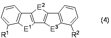
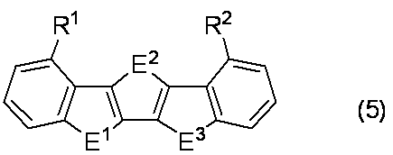
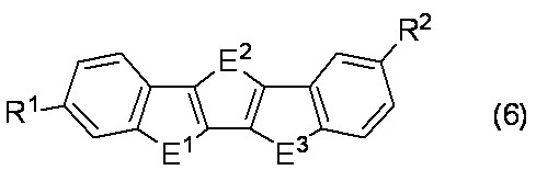
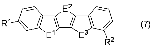
- the bonding positions of R 1 and R 2 contained in the substituted benzochalcogenoacene compound (1) of the present invention are preferably symmetrical positions.
- the symmetric position means the following formula (In the formula, E, R 1 and R 2 have the same meaning as described above.) R 1 is attached to a, R 2 is attached to a ′, R 1 is attached to b, R 2 is attached to b ′, R 1 is attached to c, and R 2 is attached to c ′.
- d 1 and R 2 may be present when d ′ has a bonding position.
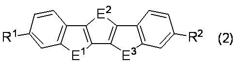
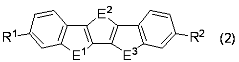
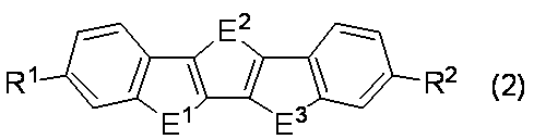
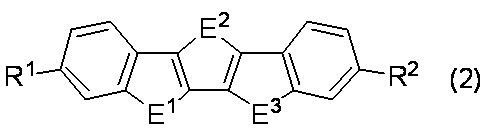
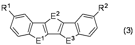
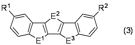
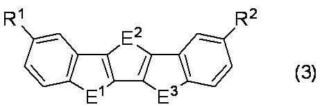
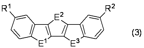
- R 1 has a bonding position at b and R 2 has a bonding position at b ′, that is, Formula (2) (In the formula, E, R 1 and R 2 have the same meaning as described above.) Or when R 1 is bonded to c and R 2 is bonded to c ′, that is, the compound represented by formula (3) (In the formula, E, R 1 and R 2 have the same meaning as described above.) The compound represented by these can be mentioned.
- a heteroaralkyl group having 5 to 30 carbon atoms which may have a fluorine atom provided that at least one of R 1 and R 2 is not a hydrogen atom).
- R 1 and R 2 are each independently an alkyl group having 4 to 30 carbon atoms which may have a fluorine atom, an alkoxy group having 4 to 30 carbon atoms which may have a fluorine atom, an alkyl group or A compound represented by the formula (1) which is an aryl group having 6 to 30 carbon atoms which may have an alkoxy group (the aryl group may have a fluorine atom); R 1 and R 2 are each independently a compound represented by the formula (1), which is an alkyl group having 4 to 30 carbon atoms or a trialkylsilyl group having 3 to 30 carbon atoms; A compound represented by formula (1) wherein R 1 and R 2 are alkyl groups having 4 to 30 carbon atoms; R 1 and R 2 are the same, and the compound represented by the formula (1), which is an alkyl group having 4 to 20 carbon atoms; A compound represented by formula (1), wherein R 1 and R 2 are each independently an alkyl group having 6 to 12 carbon atoms;
- the aryl group may have a fluorine atom
- a heteroaralkyl group having 5 to 30 carbon atoms which may have a fluorine atom
- R 1 and R 2 A compound represented by formula (2), at least one of which is not a hydrogen atom
- E independently represents a sulfur or selenium atom
- R 1 and R 2 each independently represents a hydrogen atom, an alkyl group having 4 to 30 carbon atoms or a fluorine atom optionally having a fluorine atom as a substituent.
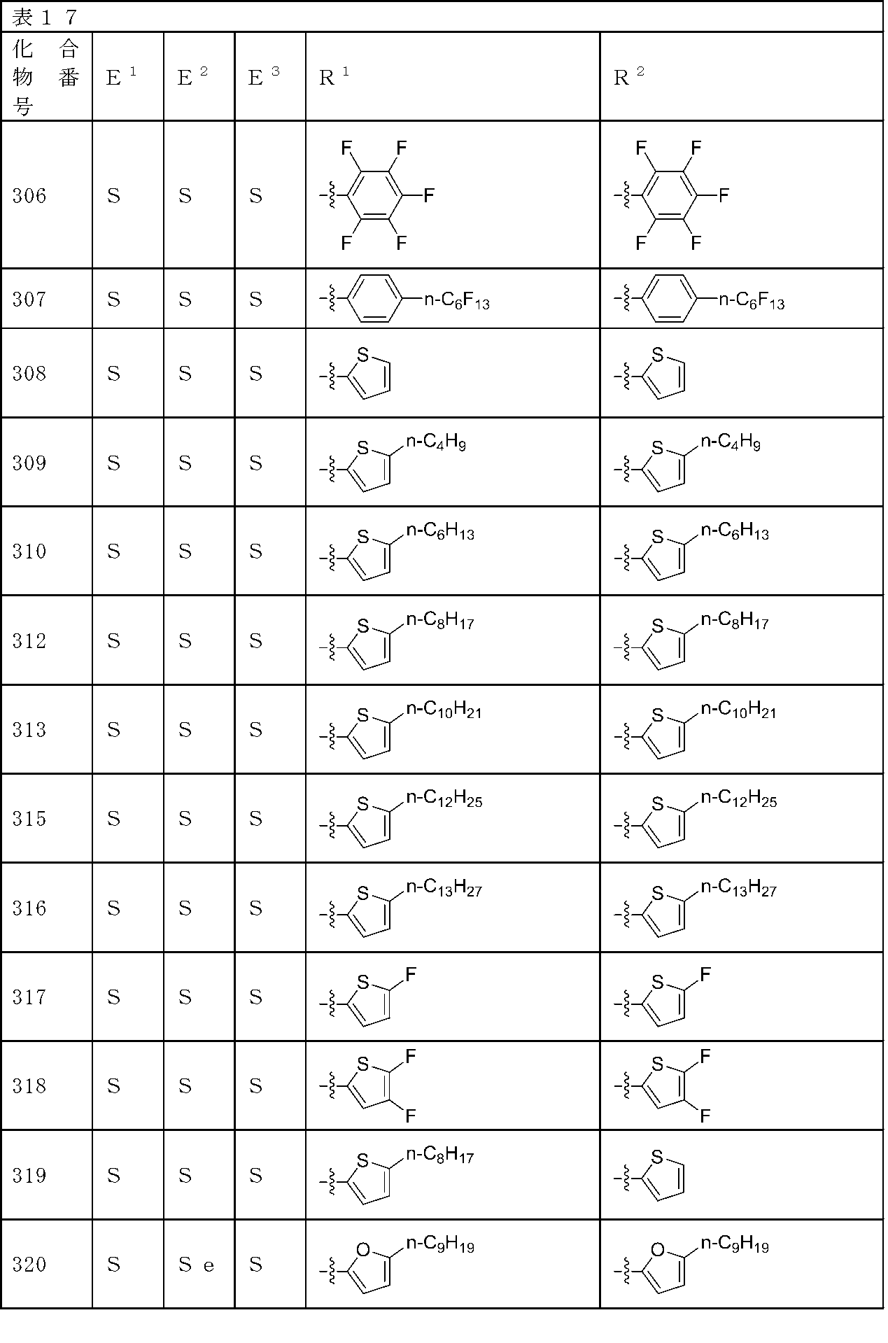
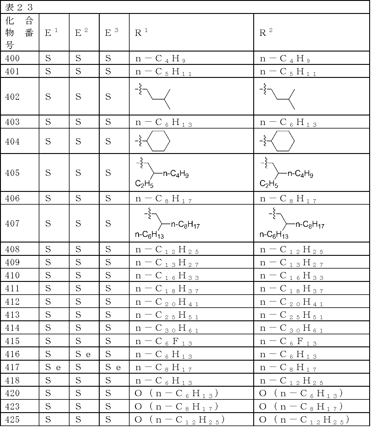
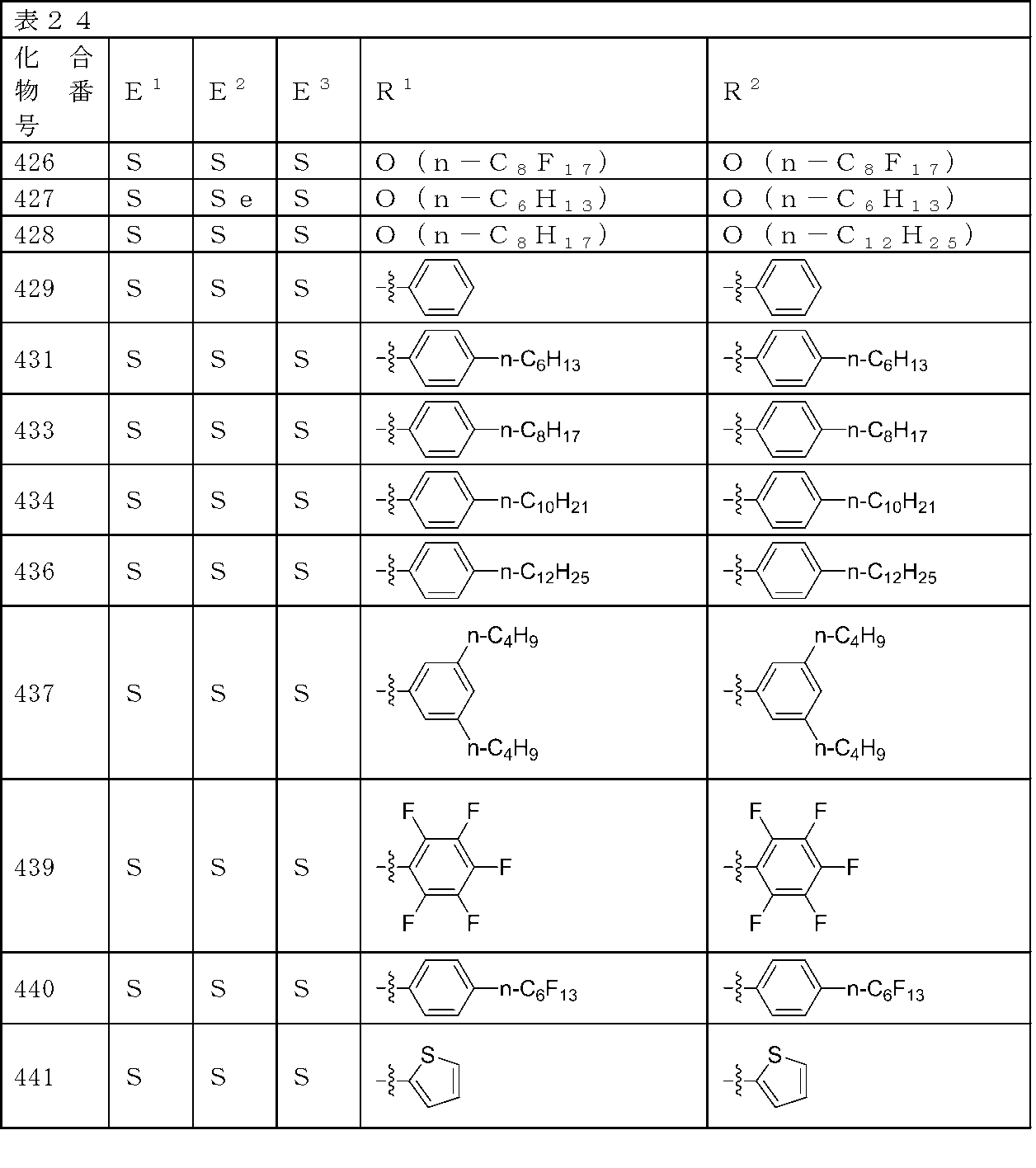
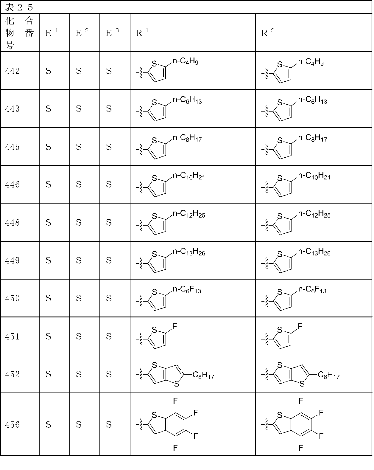
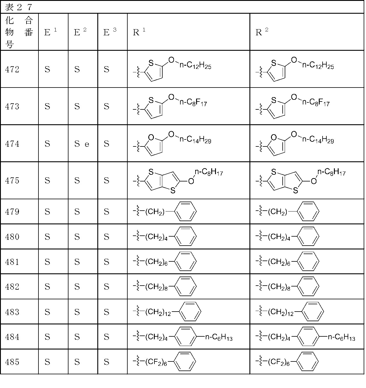
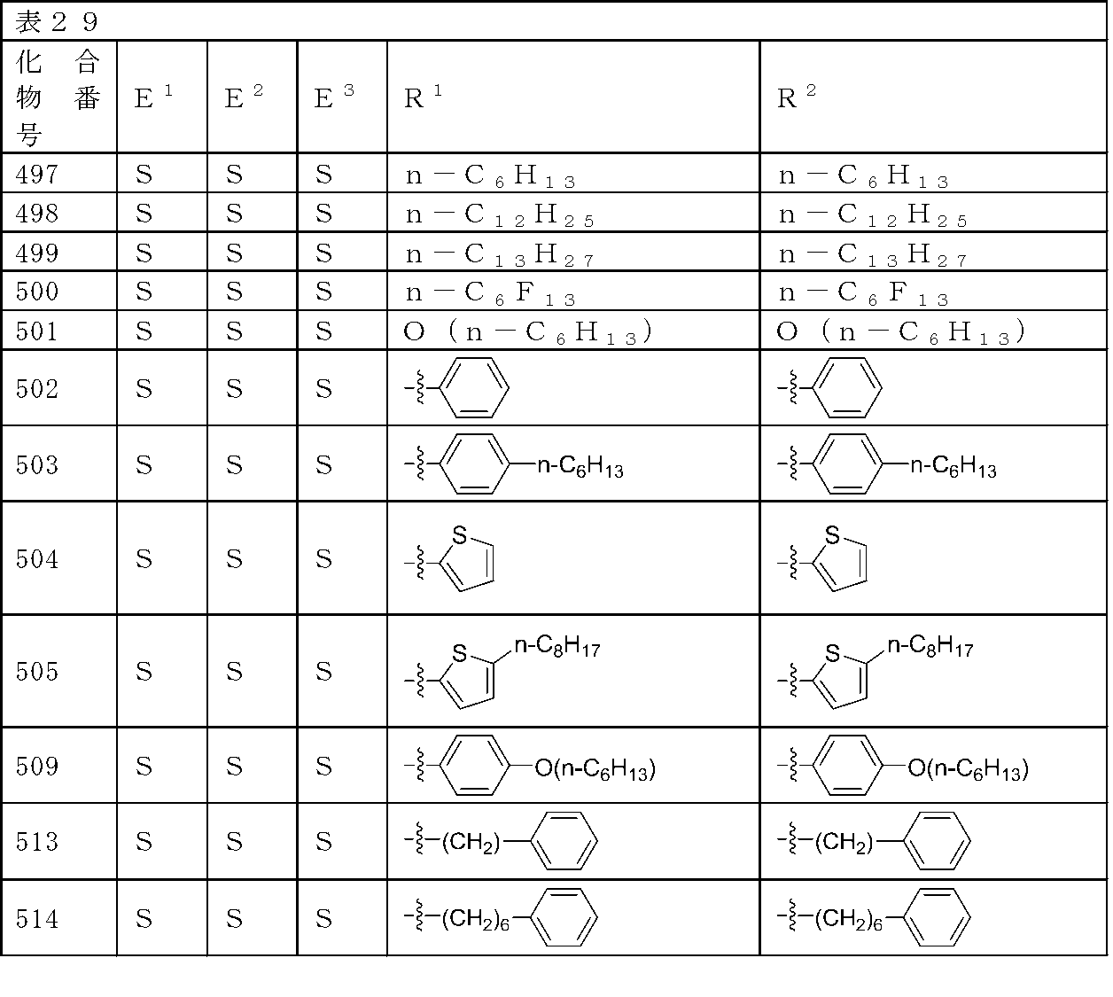
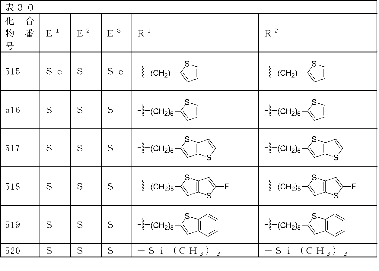
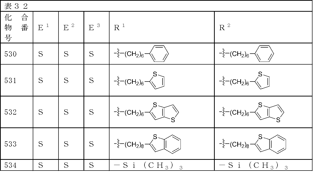
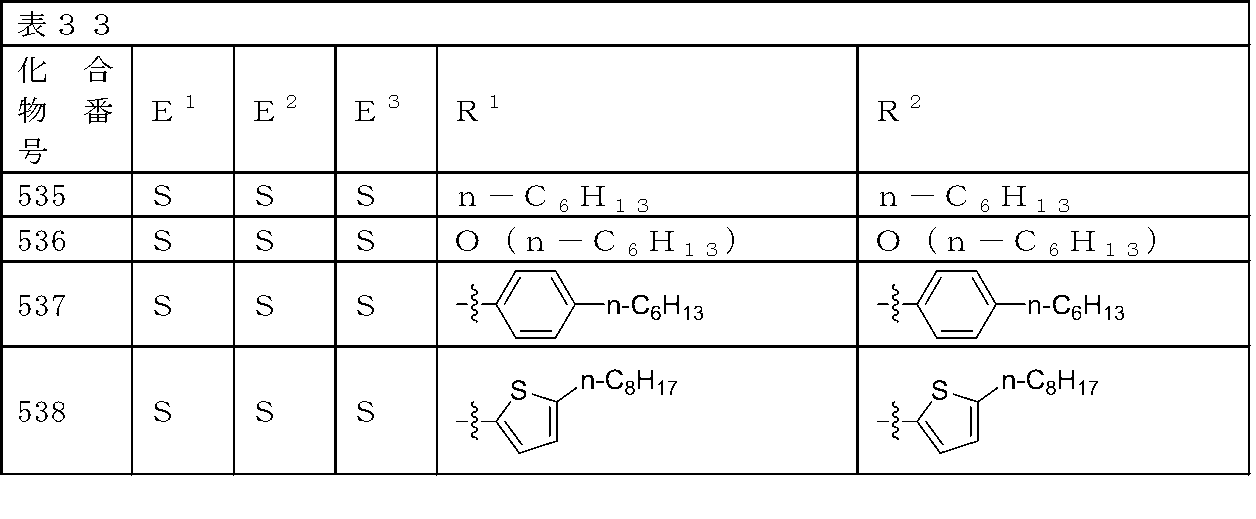
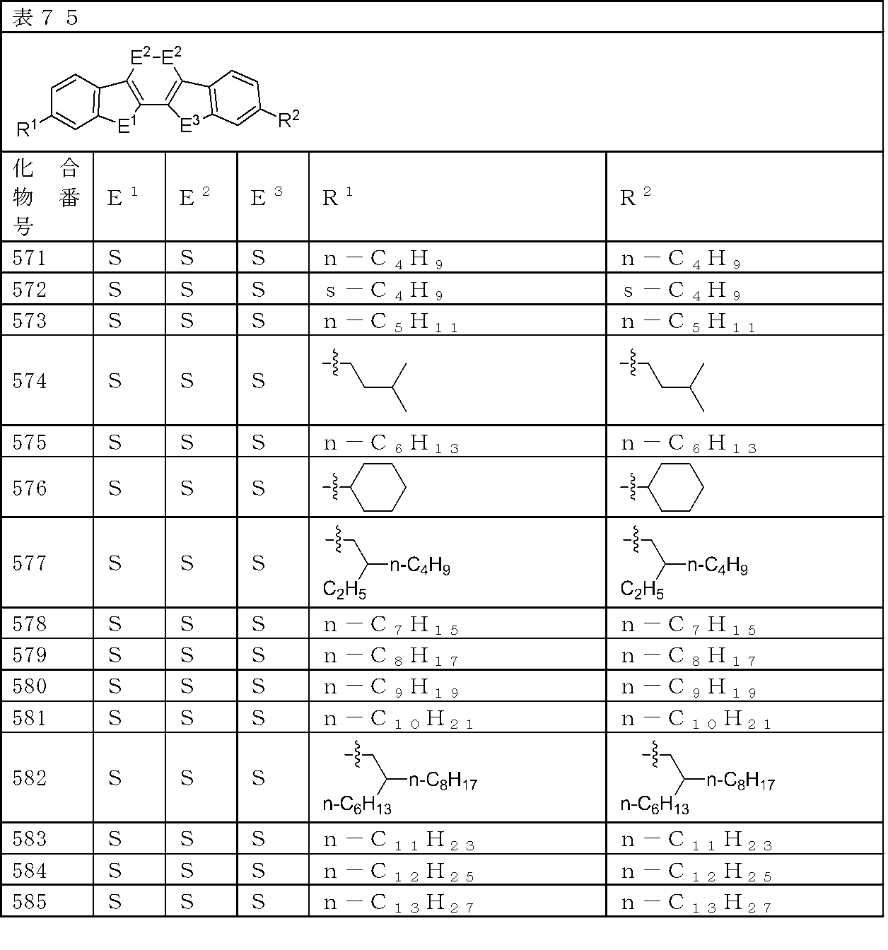
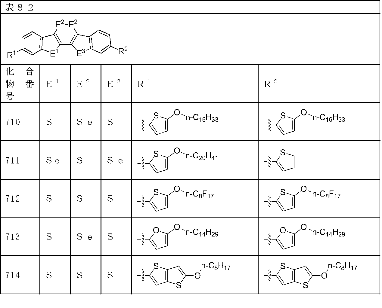
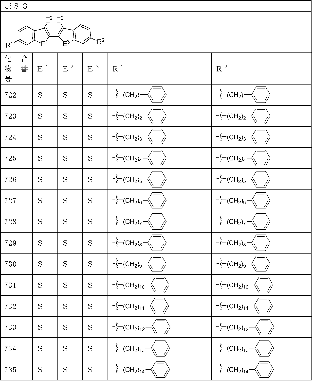
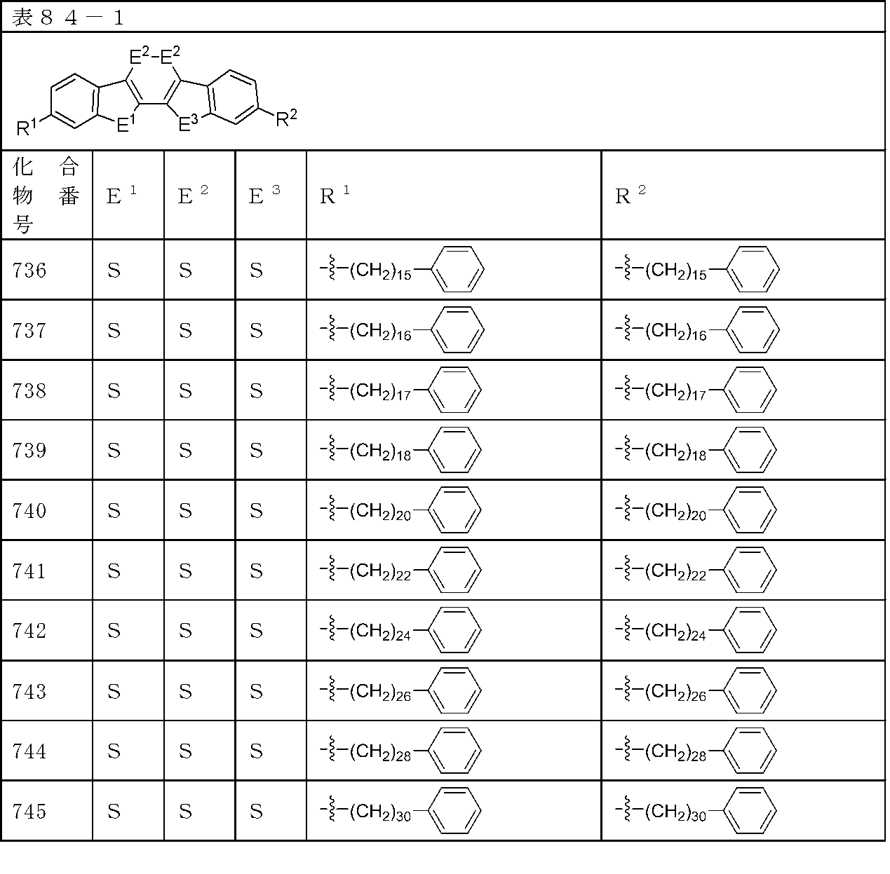
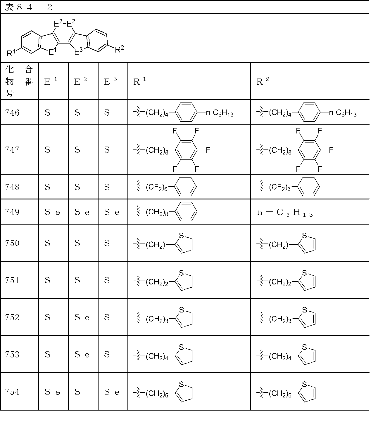
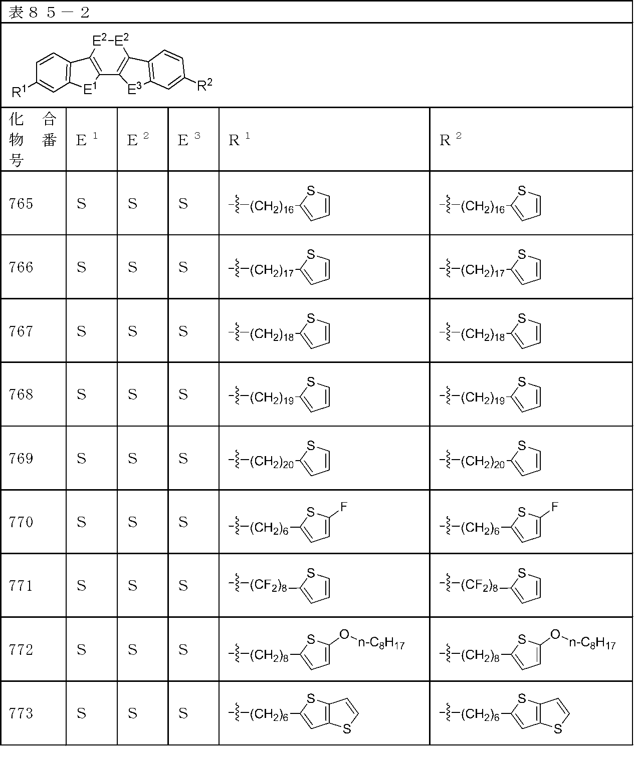
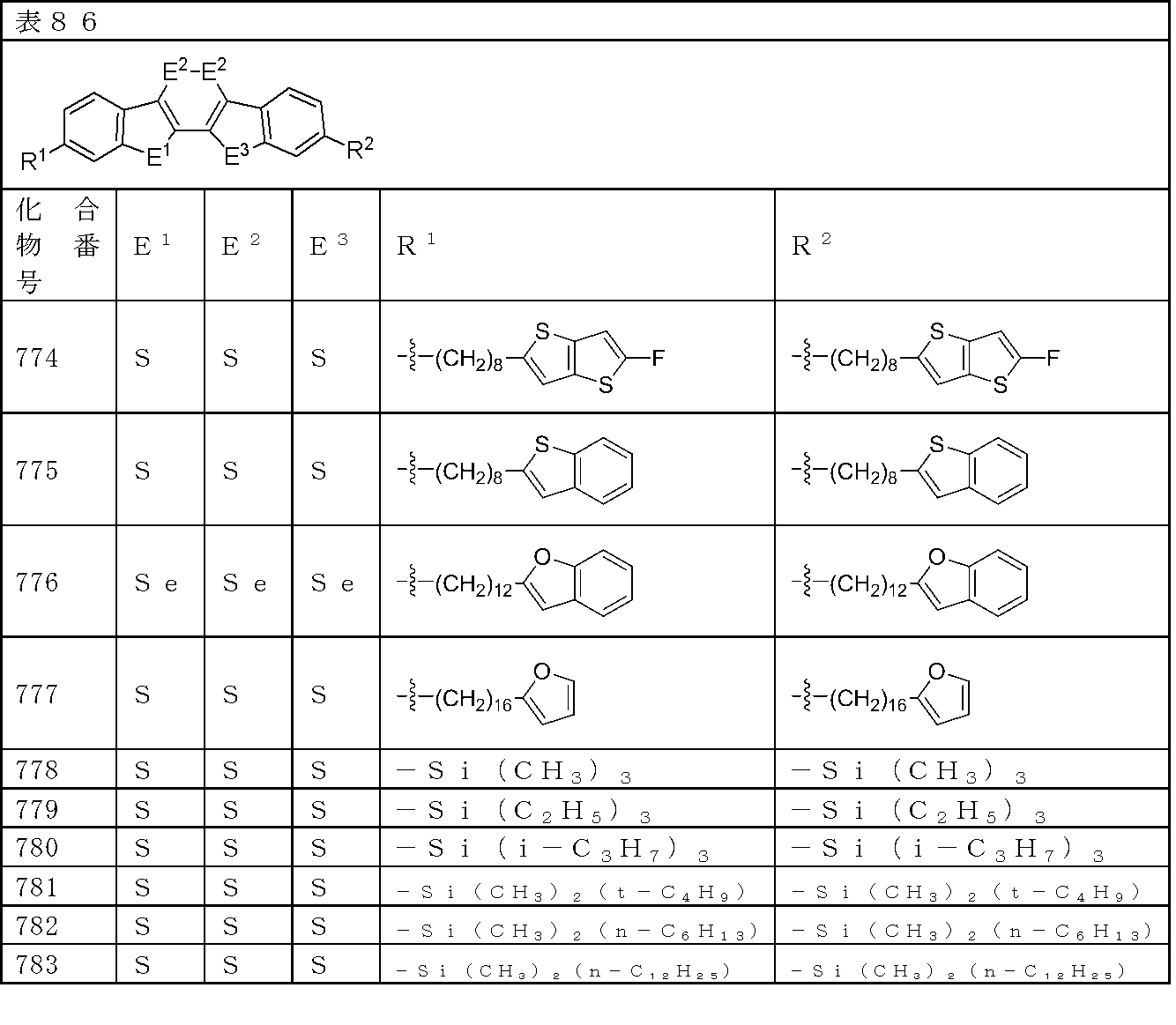
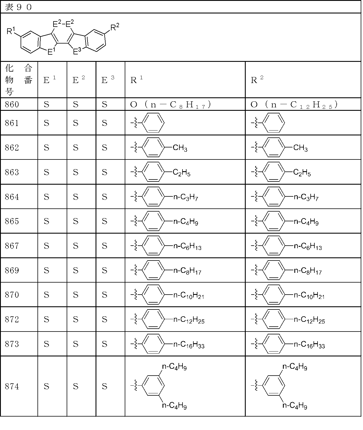
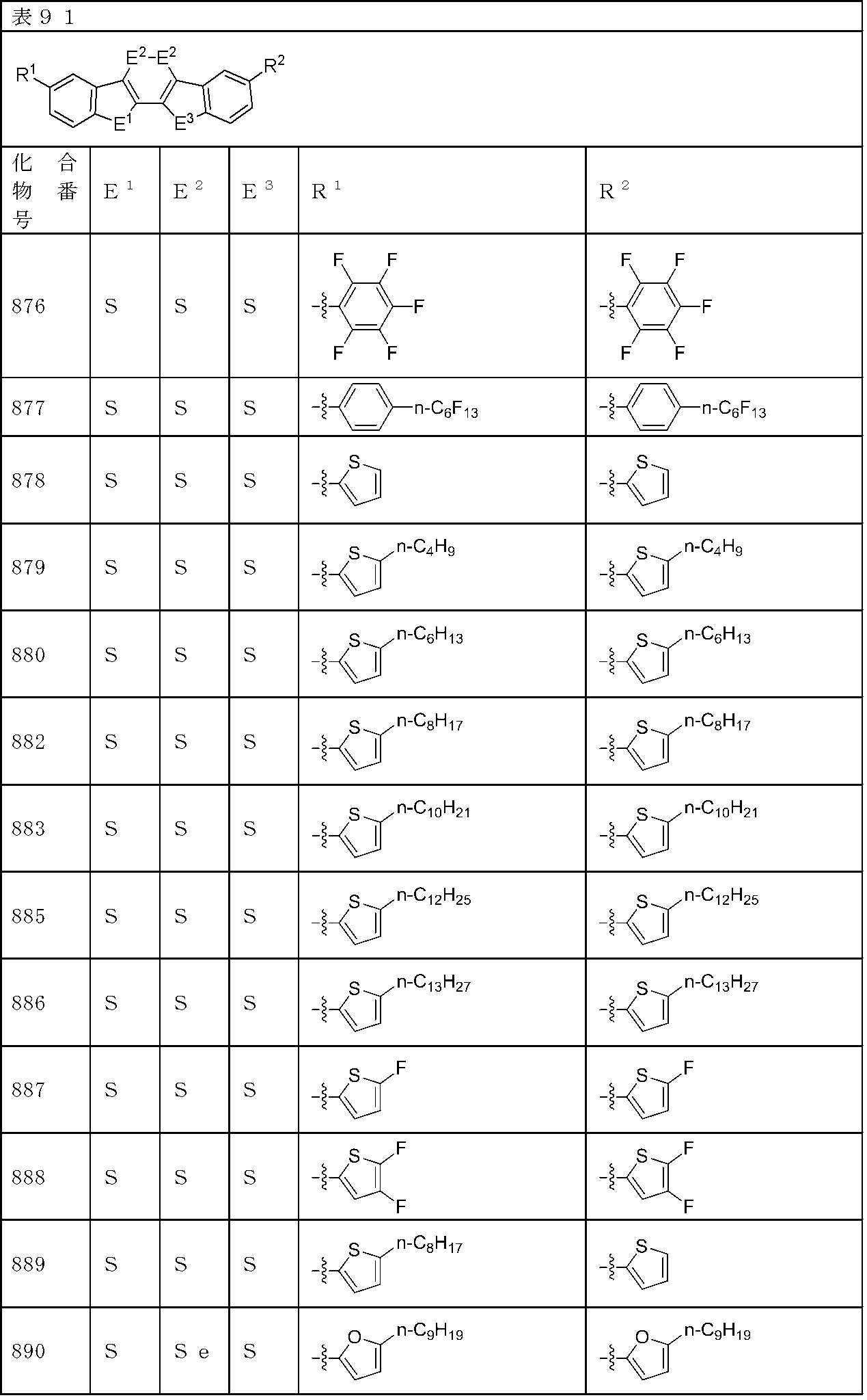
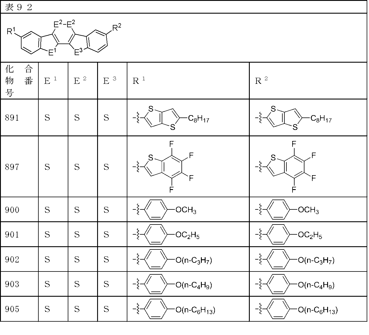
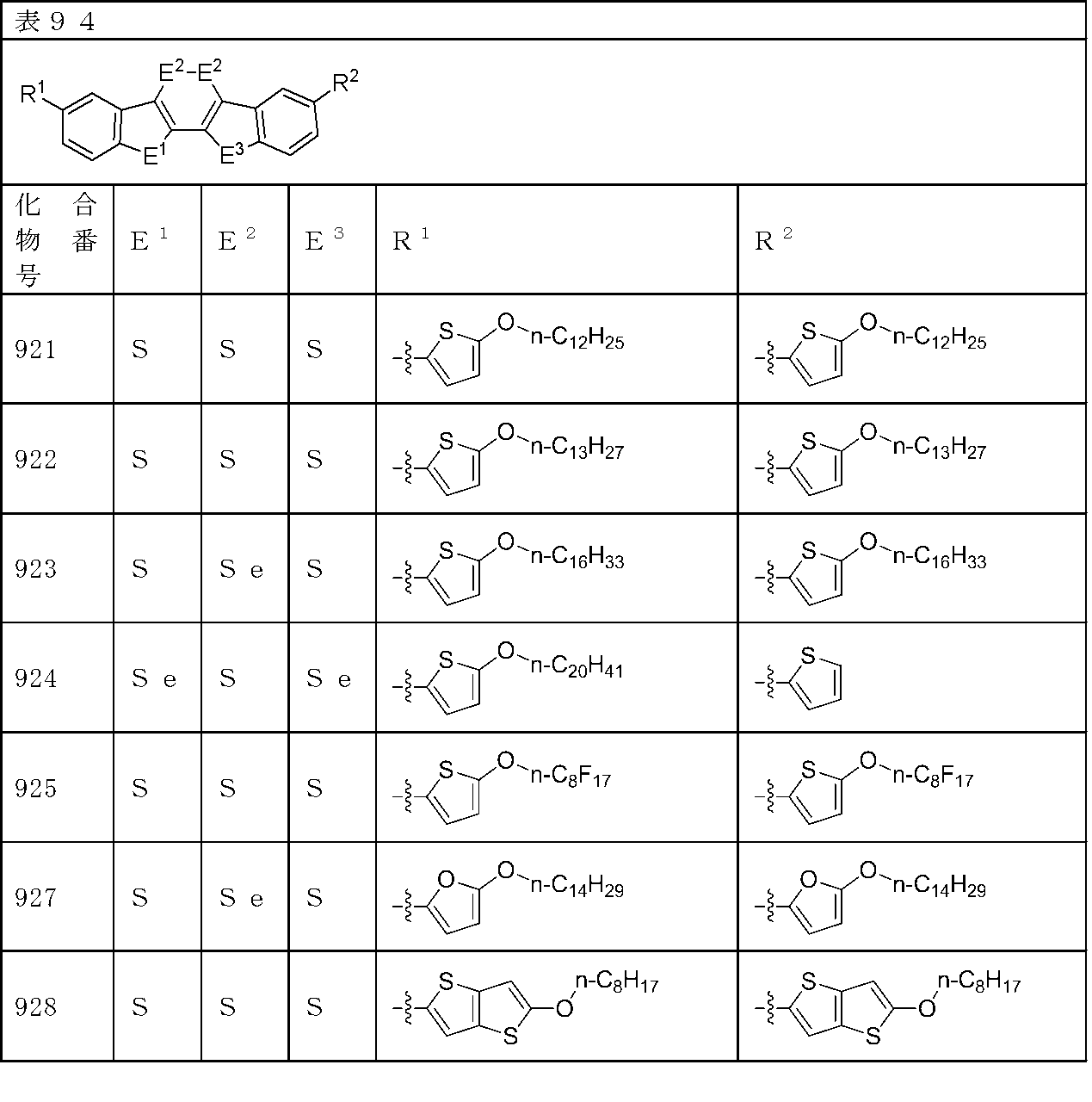
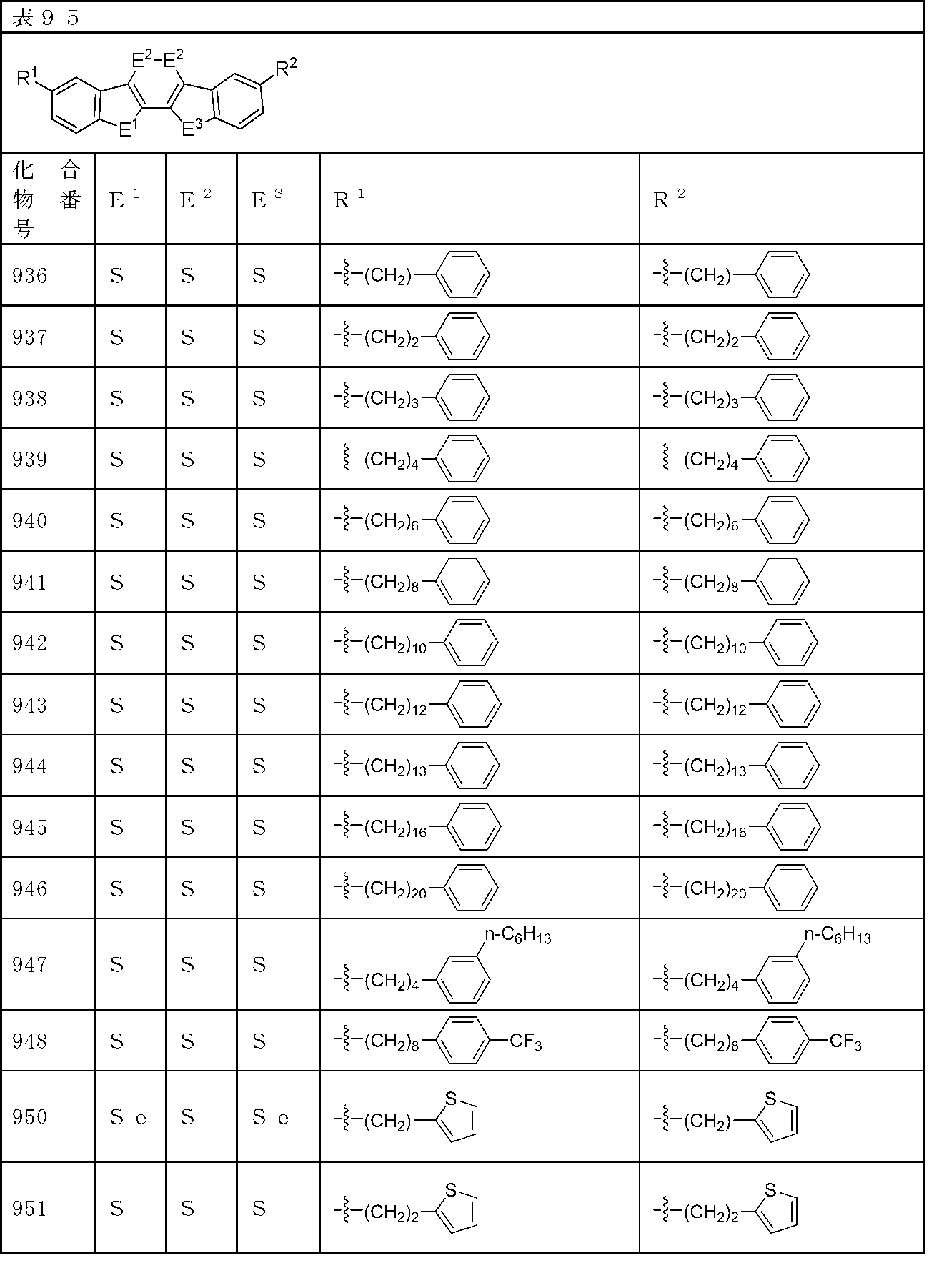
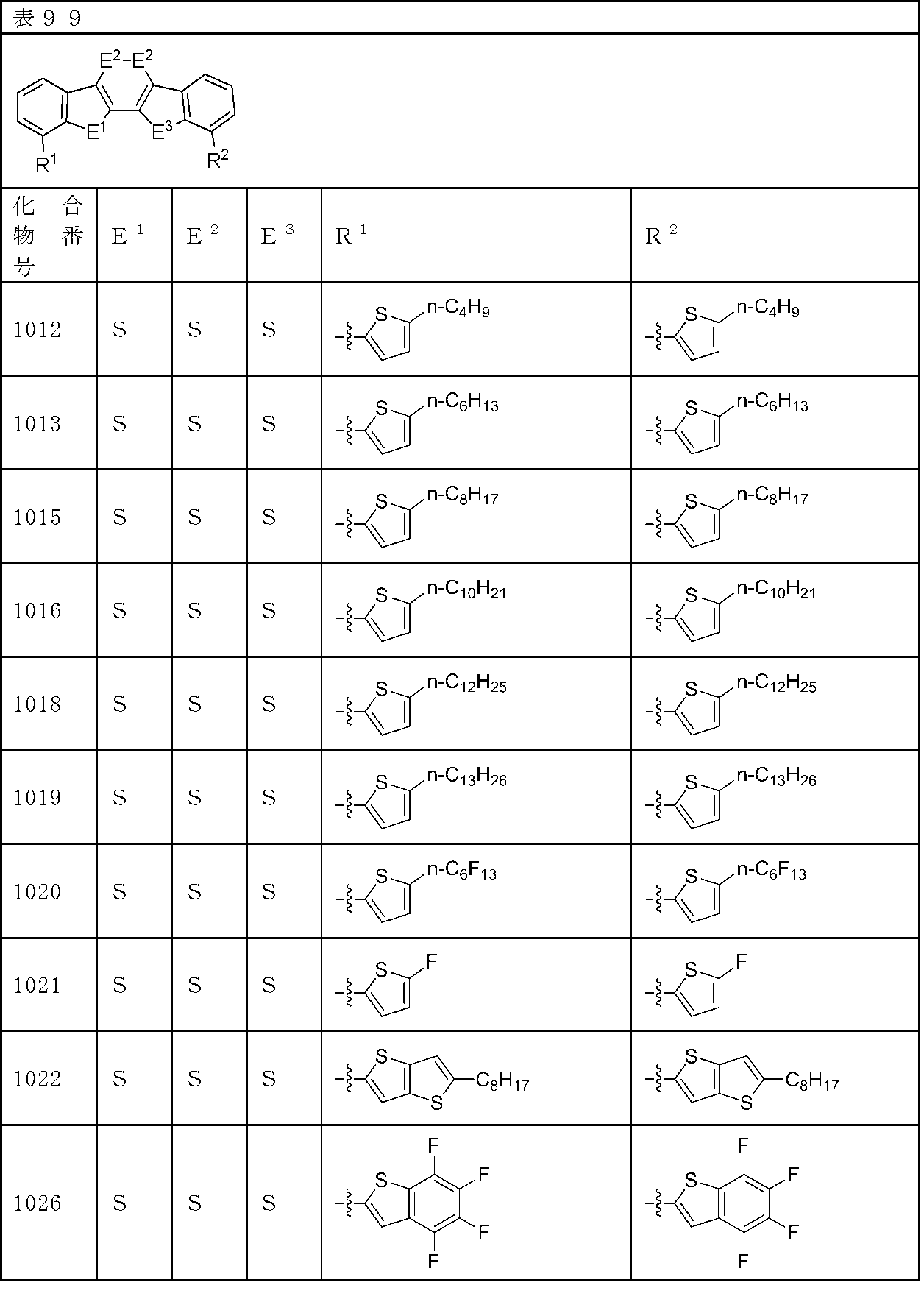
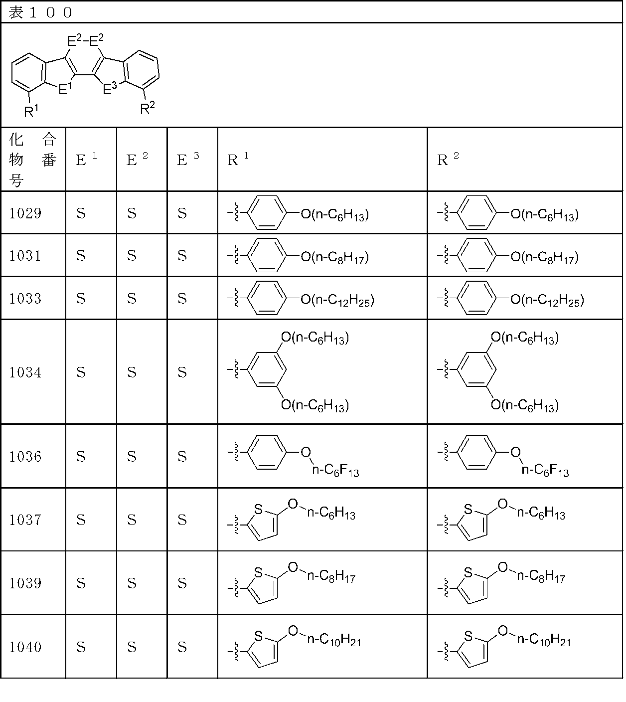
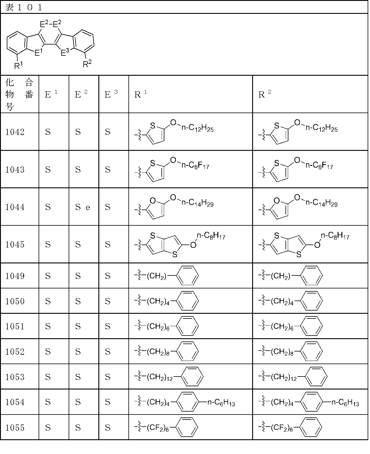
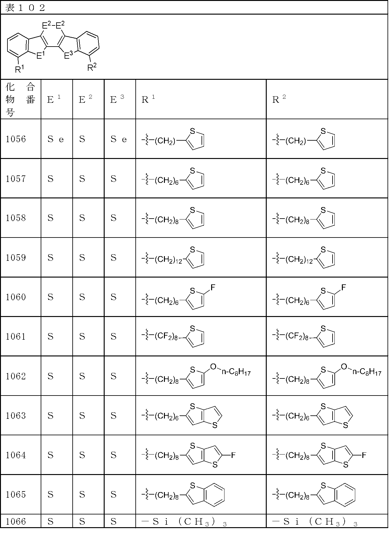
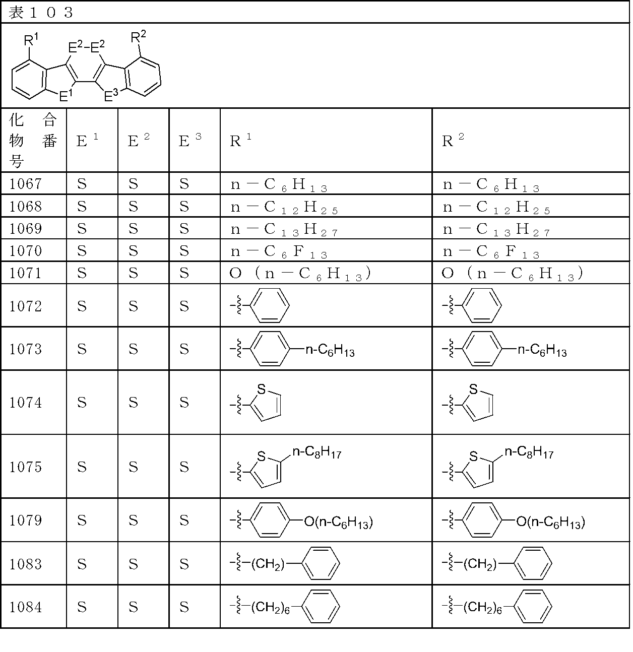
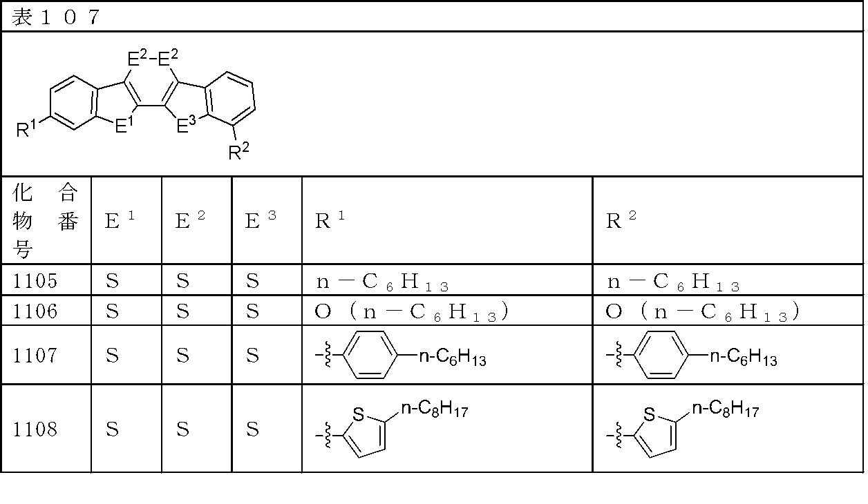
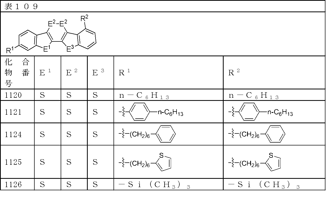
- substituted benzochalcogenoacene compound (1) of the present invention include the compounds exemplified below.
- a wavy line means a bond
- a wavy line means a bond
- a wavy line means a bond
- a wavy line means a bond
- a wavy line means a bond
- a wavy line means a bond
- a wavy line means a bond
- a wavy line means a bond
- a wavy line means a bond
- a wavy line means a bond.
- a wavy line means a bond.
- a wavy line means a bond.
- a wavy line means a bond.
- a wavy line means a bond
- a wavy line means a bond
- a wavy line means a bond
- a wavy line means a bond
- a wavy line means a bond
- a wavy line means a bond
- a wavy line means a bond
- a wavy line means a bond
- a wavy line means a bond
- a wavy line means a bond
- a wavy line means a bond
- a wavy line means a bond
- a wavy line means a bond
- a wavy line means a bond
- a wavy line means a bond
- a wavy line means a bond
- a wavy line means a bond
- a wavy line means a bond
- a wavy line means a bond
- a wavy line means a bond
- a wavy line means a bond
- a wavy line means a bond
- a wavy line means a bond
- a wavy line means a bond
- a wavy line means a bond
- a wavy line means a bond
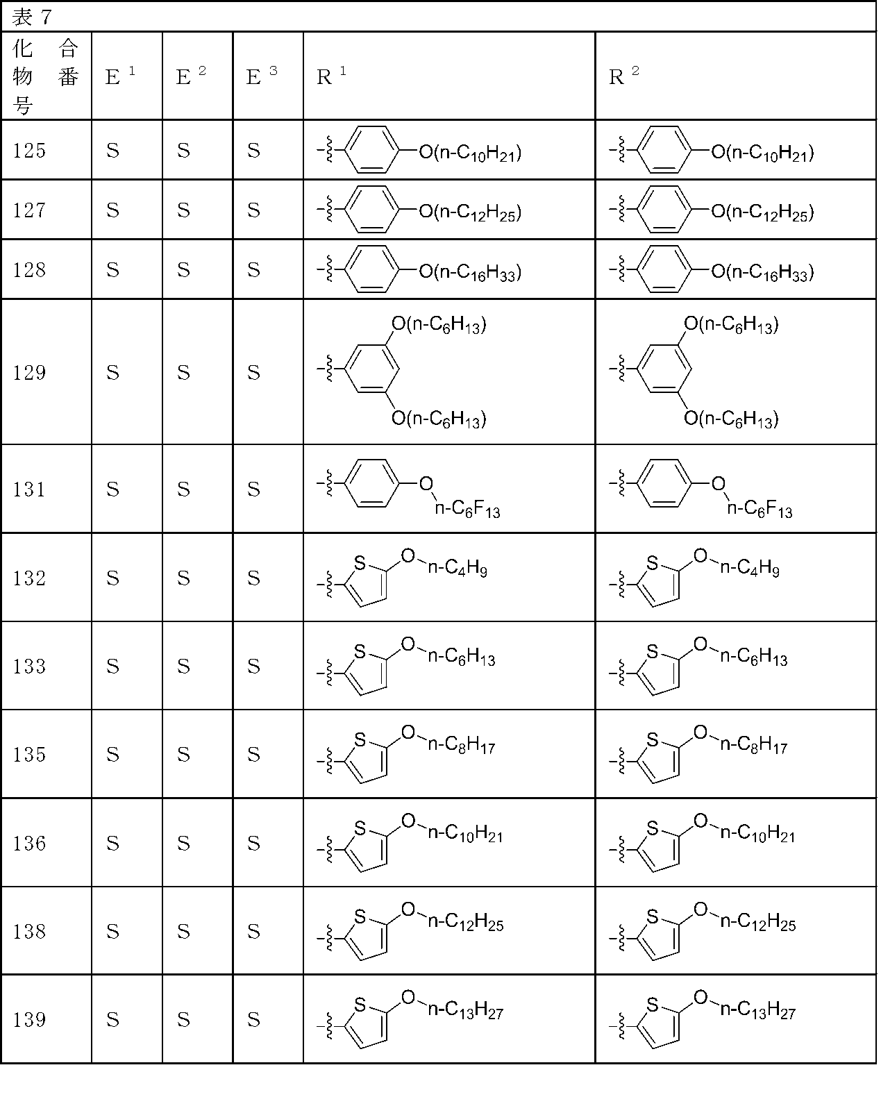
- the substituted benzochalcogenoacene compound (1) is preferably a compound in which all three Es in the substituted benzochalcogenoacene compound (1) are sulfur atoms.
- the substituted benzochalcogenoacene compound (1) having the following numbers in the table is preferable.
- the numbers in the table are the following substituted benzochalcogenoacene compounds (1). 1, 3, 4, 5, 6, 7, 8, 9, 10, 11, 12, 15, 16, 17, 18, 38, 39, 40, 41, 42, 43, 46, 47, 48, 49, 51, 52, 53, 54, 55, 56, 76, 78, 80, 81, 82, 84, 86, 87, 89, 90, 91, 95, 96, 97, 99, 100, 102, 103, 108, 118, 119, 120, 122, 124, 125, 127, 128, 129, 132, 133, 135, 136, 138, 139, 144, 152, 153, 154, 155, 156, 157, 158, 159, 160, 161, 176, 180, 181, 182, 183, 184, 185, 186, 187, 188, 189, 202, 203, 205, 206, 208, 209, 211, 214, 215,
- the substituted benzochalcogenoacene compound (1) of the present invention is excellent in solubility in an organic solvent, it can be easily handled and purified easily.
- the substituted benzochalcogenoacene compound (1) can be dissolved in an organic solvent, and coated and dried to form a thin film. Since the substituted benzochalcogenoacene compound (1) is excellent in such solvent solubility, a thin film can be easily formed by a coating film forming process described later. Further, the substituted benzochalcogenoacene compound (1) is described later. In addition, a thin film exhibiting high carrier mobility can be provided.
- the first reaction it is referred to as “the first reaction”), and then, by reacting with sulfur or selenium, the formula (4-1) (In the formula, E, R 1 and R 2 represent the same meaning as described above.)
- a dichalcogenin compound (sometimes referred to as compound (4-1)) was obtained (hereinafter, this reaction is referred to as “the second reaction”).
- organometallic base used in the first reaction examples include methyl lithium (MeLi), n-butyl lithium (n-BuLi), sec-butyl lithium (sec-BuLi), and tert-butyl lithium (t-BuLi).
- Organolithium compounds such as, and organomagnesium compounds such as alkyl Grignard compounds can be used.
- the organometallic base is preferably an organolithium compound, For example, butyl lithium (BuLi) is used, and more preferably t-BuLi is used.
- the amount of the organometallic base used can be, for example, in the range of 4 to 20 mol per mol of the compound (5-1) (in the range of 2 to 10 times equivalent to the halogen atom), preferably A range of 6 to 14 moles (a range of 3 to 7 times equivalent to halogen atoms), and a range of 7 to 10 moles (a range of 3.5 to 5 times equivalents to halogen atoms) is more preferable.
- the amount of the organometallic base used is 4 mol or more, the unreacted compound (5-1) is reduced and the yield of the resulting compound (4-1) tends to be improved.
- the amount used is 20 mol or less, the progress of the side reaction tends to be suppressed and the purification of the compound (4-1) tends to be easy.
- the first reaction and the subsequent second reaction are preferably performed in the presence of a solvent.
- the solvent used is selected from those which do not significantly disturb the progress of the first reaction and the second reaction.
- aliphatic hydrocarbons such as pentane, hexane and heptane, and aromatics such as benzene, toluene and xylene.
- An aromatic hydrocarbon solvent, an ether solvent such as diethyl ether and tetrahydrofuran (THF), or a mixed solvent of two or more selected from them is used.
- a preferred solvent is an ether solvent.
- This first reaction is carried out, for example, at a reaction temperature of ⁇ 20 ° C. or lower, preferably ⁇ 40 ° C. or lower, more preferably ⁇ 60 ° C. or lower.
- reaction time of this 1st reaction can be adjusted with the kind of organometallic base and solvent to be used, or reaction temperature, it is the range of about 10 minutes to 5 hours.
- sulfur or selenium is added to the reaction mixture to perform the second reaction.
- Sulfur (or selenium) to be used may be used as a solid, or may be added as a solution or suspension dissolved or suspended in the solvent used in the first reaction.
- the reaction temperature may be maintained at the same level as in the first reaction, or may be heated as long as it is within the boiling point of the solvent used.
- the reaction temperature is raised until it reaches the range of 0 to 40 ° C., and the temperature is kept within the same range.
- An example of the reaction time is 30 minutes to 72 hours.
- the sulfur or selenium used in the second reaction crystalline, powdery, colloidal sulfur (or selenium) or the like can be used.
- the amount of sulfur (or selenium) to be used can be, for example, in the range of 4 to 20 mol, preferably in the range of 6 to 14 mol, more preferably in the range of 7 to 1 with respect to 1 mol of compound (5-1). A range of 10 moles is mentioned.
- the amount of sulfur (or selenium) used is 4 mol or more, the yield of the compound (4-1) tends to be improved, and when it is 20 mol or less, the progress of side reactions is suppressed,
- the compound (4-1) is preferred because it tends to be easily purified.
- the solvent is concentrated if necessary, and an alkaline aqueous solution such as an aqueous sodium hydroxide solution or an aqueous potassium hydroxide solution is added to the obtained reaction mixture, and then the obtained compound (4-1) To extract.
- an alkaline aqueous solution such as an aqueous sodium hydroxide solution or an aqueous potassium hydroxide solution is added to the obtained reaction mixture, and then the obtained compound (4-1) To extract.
- the extraction solution can be used as the extraction solvent as it is, but preferred extraction solvents are halogenated compounds such as dichloromethane and chloroform. A hydrocarbon solvent is mentioned.
- the aqueous phase is separated, an aqueous hexacyanoferrate solution such as potassium ferricyanate is added to the aqueous phase, and the compound (4-1) is added from the aqueous phase. Extraction is performed using an organic solvent such as the extraction solvent.
- the compound (4-1) thus obtained may be further purified by an operation such as column chromatography or recrystallization as necessary.
- this 3-1 reaction for example, 0.5 to 20 mol, preferably 1 to 10 mol, more preferably 2 to 7 mol of copper compound or platinum compound is used per 1 mol of compound (4-1). It is done.
- the copper compound include copper powder
- examples of the platinum compound include biscyclooctadienyl platinum (Pt (COD) 2 ).
- the reaction temperature of this 3-1 reaction can be, for example, in the range of 150 to 400 ° C., preferably in the range of 200 to 370 ° C.
- the reaction time of this 3-1 reaction is within 1 hour, preferably within 30 minutes. After completion of the reaction, the reaction mixture is cooled to room temperature.
- insoluble impurities are filtered off using a solvent capable of dissolving the substituted benzochalcogenoacene compound (1), such as chloroform and dichloromethane, and the filtrate is concentrated. Accordingly, the substituted benzochalcogenoacene compound (1) is obtained by performing operations such as column chromatography and recrystallization.
- a solvent capable of dissolving the substituted benzochalcogenoacene compound (1) such as chloroform and dichloromethane
- the nickel compound used is preferably a zerovalent nickel compound such as biscyclooctadienyl nickel (Ni (COD) 2 ).
- This 3-2 reaction generates zero-valent nickel compounds in the system by reacting bisacetylacetonate nickel (Ni (acac) 2 ), which is a divalent nickel compound, with a reducing agent such as diisobutylaluminum hydride. You may let them.
- the amount of the nickel compound used can be, for example, in the range of 0.5 to 5 mol, preferably in the range of 0.7 to 3 mol, per 1 mol of compound (4-1).
- Examples of the phosphine compound include triphenylphosphine, tricyclohexylphosphine, tri (o-tolyl) phosphine, trimethylphosphine, tri-t-butylphosphine, 1,2- (diphenylphosphino) ethane, and 1,3- (diphenyl).
- Examples thereof include phosphino) propane, 1,4- (diphenylphosphino) butane and 1,1-bis (diphenylphosphino) ferrocene, and triphenylphosphine is preferred.
- the amount of the phosphine compound used may be, for example, in the range of 0.5 to 20 mol of the phosphine compound, and preferably in the range of 0.7 to 10 mol, with respect to 1 mol of the nickel compound.
- Examples of the solvent used in the present 3-2 reaction include aliphatic hydrocarbon solvents such as pentane, hexane and heptane, aromatic hydrocarbon solvents such as benzene, toluene and xylene, and halogenated hydrocarbons such as dichloromethane and chloroform. A solvent etc. can be mentioned. These solvents may be used alone or as a mixed solvent of two or more. As the solvent, an aromatic hydrocarbon solvent is preferable, and toluene is more preferable.
- Examples of the reaction temperature of the present 3-2 reaction include a range of 10 ° C. to the boiling point of the solvent or less. The reaction time of the present 3-2 reaction depends on the reaction temperature, but is preferably within 72 hours.
- a wavy line means a bond
- a wavy line means a bond
- a wavy line means a bond
- a wavy line means a bond
- a wavy line means a bond
- a wavy line means a bond
- a wavy line means a bond
- a wavy line means a bond
- a wavy line means a bond.
- a wavy line means a bond.
- a wavy line means a bond.
- a wavy line means a bond.
- a wavy line means a bond
- a wavy line means a bond
- a wavy line means a bond
- a wavy line means a bond
- a wavy line means a bond
- a wavy line means a bond.
- a wavy line means a bond.
- a wavy line means a bond
- a wavy line means a bond
- a wavy line means a bond
- a wavy line means a bond.
- a wavy line means a bond.
- a wavy line means a bond.
- a wavy line means a bond.
- a wavy line means a bond
- a wavy line means a bond
- a wavy line means a bond
- a wavy line means a bond
- a wavy line means a bond
- a wavy line means a bond
- a wavy line means a bond
- a wavy line means a bond
- a wavy line means a bond
- a wavy line means a bond
- a wavy line means a bond
- a wavy line means a bond
- a wavy line means a bond
- a wavy line means a bond
- a wavy line means a bond
- a wavy line means a bond
- a wavy line means a bond
- a wavy line means a bond
- a wavy line means a bond
- a wavy line means a bond
- a wavy line means a bond
- a wavy line means a bond
- a wavy line means a bond
- a wavy line means a bond.
- a wavy line means a bond.
- a wavy line means a bond.
- a wavy line means a bond.
- a wavy line means a bond
- a wavy line means a bond
- a wavy line means a bond
- a wavy line means a bond
- a wavy line means a bond
- a wavy line means a bond
- a wavy line means a bond
- a wavy line means a bond
- a wavy line means a bond
- a wavy line means a bond
- a wavy line means a bond.
- a wavy line means a bond.
- a wavy line means a bond
- a wavy line means a bond
- a wavy line means a bond
- a wavy line means a bond
- a wavy line means a bond
- a wavy line means a bond
- a wavy line means a bond
- a wavy line means a bond
- a wavy line means a bond
- a wavy line means a bond
- a wavy line means a bond
- a wavy line means a bond
- a wavy line means a bond
- a wavy line means a bond
- a wavy line means a bond
- R 1 and R 2 contained in the compound (5-1) are the same type of group (hereinafter, sometimes referred to as R).
- R represents the same meaning as R 1 and R 2, and X represents a halogen atom, preferably a bromine atom.
- the so-called Glaser Reaction, Eglinton Coupling or Hay Coupling preferably Hay coupling using a copper compound such as copper iodide is used.
- Hay coupling can be performed in the presence of a copper compound such as N, N, N ′, N′-tetramethylethylenediamine (TMEDA) and copper iodide, as shown below.
- TEDA N, N, N ′, N′-tetramethylethylenediamine
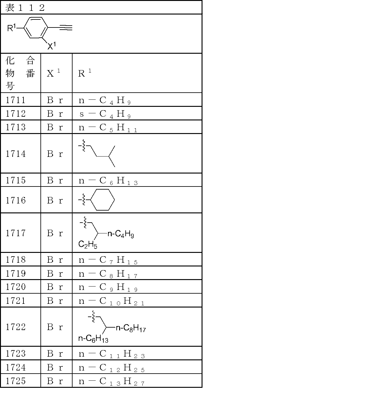
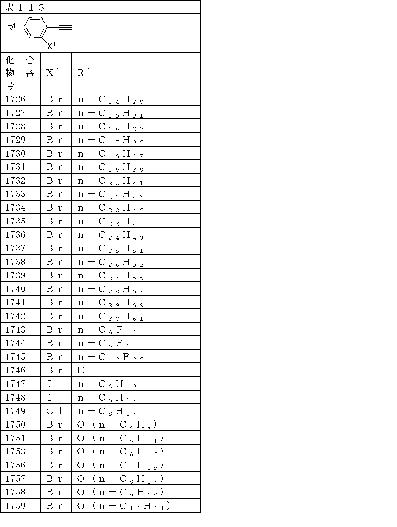
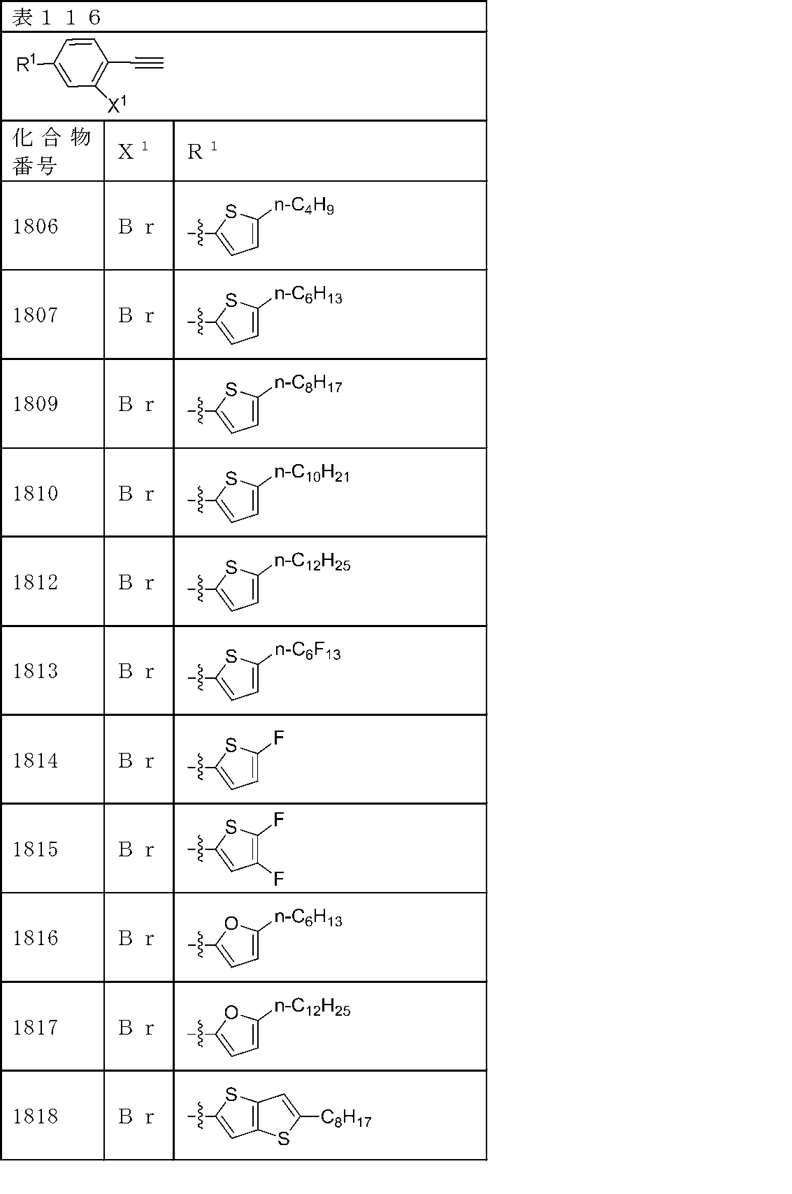
- the compound of formula (6-1) is obtained by, for example, brominating an aniline having a substituent R with ⁇ -position of an amino group with N-bromosuccinimide or the like, and subjecting the amino group of the obtained compound to a Sandmeyer reaction. And the like, and a method of ethynylating the iodo group of the obtained iodo group-containing compound by an ethynylation reaction such as a Sonogashira cross-coupling reaction.
- a wavy line means a bond
- a wavy line means a bond
- a wavy line means a bond
- a wavy line means a bond
- a wavy line means a bond
- a wavy line means a bond
- a wavy line means a bond
- a wavy line means a bond
- a wavy line means a bond.
- a wavy line means a bond.
- a wavy line means a bond.
- a wavy line means a bond.
- a wavy line means a bond
- a wavy line means a bond
- a wavy line means a bond
- a wavy line means a bond
- a wavy line means a bond
- a wavy line means a bond.
- a wavy line means a bond.
- a wavy line means a bond
- a wavy line means a bond
- a wavy line means a bond
- a wavy line means a bond.
- a wavy line means a bond.
- a wavy line means a bond.
- a wavy line means a bond.
- a wavy line means a bond
- a wavy line means a bond
- a wavy line means a bond
- a wavy line means a bond
- a wavy line means a bond
- a wavy line means a bond
- a wavy line means a bond
- Non-Patent Document 1 As a production method in the case where R 1 and R 2 contained in the substituted benzochalcogenoacene compound (1) are the same or different groups, for example, Non-Patent Document 1 (Advanced Materials, 19 , 3008-3011) (2007)) can be mentioned. That is, as shown in the following formula, after bromination of benzo [b] thiophene having R 1 or R 2 with bromine, lithium diisopropylamide (LDA) was allowed to act on the obtained brominated product, and then copper chloride Next, butyllithium (BuLi) and bis (phenylsulfonyl) sulfide ((C 6 H 5 SO 2 ) 2 S) are allowed to act on the obtained coupling product to produce compound (1). It is a method to do.
- LDA lithium diisopropylamide
- the thin film of the present invention contains a substituted benzochalcogenoacene compound (1). Since the thin film exhibits high carrier mobility, it is suitable as a material for an organic semiconductor device having the thin film as an organic semiconductor active layer. Moreover, the organic-semiconductor device of this invention contains the thin film of this invention.
- an organic semiconductor device of this invention an organic transistor, an electroluminescent element, a solar cell etc. can be mentioned, for example.
- the organic transistor of this invention can be used for an electronic paper, a flexible display, an IC tag, a sensor, etc., for example.
- Examples of the method for forming a thin film of the present invention include a coating film forming process.
- the coating film forming process means a film forming process including a step of dissolving the substituted benzochalcogenoacene compound (1) in a solvent and applying the obtained solution composition to a substrate or an insulator layer.
- Examples of the coating method include a casting method, a dip coating method, a die coater method, a roll coater method, a bar coater method, a spin coating method, an ink jet method, a screen printing method, an offset printing method, and a micro contact printing method. These methods may be used alone or in combination of two or more.
- an optimum solvent can be selected according to the kind of the substituted benzochalcogenoacene compound (1) to be applied.
- benzene, toluene, xylene, chlorobenzene is used.
- Aromatic hydrocarbon solvents such as o-dichlorobenzene, halogenated aliphatic hydrocarbon solvents such as dichloromethane, chloroform, 1,2-dichloroethane, 1,1 ′, 2,2′-tetrachloroethane, carbon tetrachloride,
- ether solvents such as tetrahydrofuran and dioxane
- aliphatic hydrocarbon solvents such as pentane, hexane, pentane, octane, and cyclohexane, among which toluene, xylene, o-dichlorobenzene, dichloromethane, chloroform, tetrahydrofuran, and hexane are preferable.
- the concentration of the substituted benzochalcogenoacene compound (1) in the solution composition is 0.001 to 50% by weight, preferably 0.01 to 10% by weight, more preferably 0.1 to 5% by weight.
- the solution composition may contain additives such as antioxidants and stabilizers as long as the mobility of the resulting thin film is not significantly impaired.
- the solution composition can be prepared by dissolving the substituted benzochalcogenoacene compound (1) in a solvent at, for example, about 10 to 200 ° C., preferably about 20 to 150 ° C.
- a solvent contained in the coating film is removed to form a thin film on the substrate or the insulating layer.
- natural drying treatment, heat treatment, reduced pressure treatment, ventilation treatment or a combination thereof is employed, but natural drying treatment or heat treatment is preferred in terms of simple operation.
- a hot plate for example, 40 to 250 ° C., preferably 50 to 200 ° C.
- the thin film of the present invention can be formed by coating film formation using a dispersion in which the substituted benzochalcogenoacene compound (1) is dispersed in a solvent.
- the above-described coating film forming process can be easily performed by replacing the solution composition with the dispersion liquid.
- the thin film of the present invention can be formed by a simple method such as the above-described coating film forming process.
- a method for forming a thin film by subjecting the substituted benzochalcogenoacene compound (1) to a vacuum process such as a vacuum deposition method, a sputtering method, a CVD method, or a molecular beam epitaxial growth method.
- a vacuum process such as a vacuum deposition method, a sputtering method, a CVD method, or a molecular beam epitaxial growth method.
- a method for forming a thin film by a vacuum deposition method is a method in which a substituted benzochalcogenoacene compound is heated in a crucible or a metal boat under vacuum, and an evaporated organic semiconductor material is deposited on a substrate or an insulator material.
- the degree of vacuum at the time of vapor deposition is usually 1 ⁇ 10 ⁇ 1 Pa or less, preferably 1 ⁇ 10 ⁇ 3 Pa or less.
- the substrate temperature at the time of vapor deposition is usually 0 ° C to 300 ° C, preferably 20 ° C to 200 ° C. Examples of the vapor deposition rate include a range of 0.001 nm / sec to 10 nm / sec, and preferably 0.01 nm / sec to 1 nm / sec.
- the film thickness of the thin film containing the substituted benzochalcogenoacene compound (1) obtained by the coating film forming process or the vacuum process can be appropriately adjusted depending on, for example, the element structure of the organic transistor, but preferably 1 nm to 10 ⁇ m. More preferably, the thickness is 5 nm to 1 ⁇ m.
- Examples of the organic transistor of the present invention include an organic field effect transistor (OFET).
- the structure of the organic field effect transistor is usually such that a source electrode and a drain electrode are provided in contact with an organic semiconductor active layer comprising the thin film of the present invention, and an insulating layer (dielectric layer) in contact with the organic semiconductor active layer. It is only necessary that a gate electrode be provided with a gap therebetween.
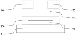
- As the element structure for example, (1) Structure of substrate / gate electrode / insulator layer / source electrode / drain electrode / organic semiconductor active layer (see FIG. 1), (2) Structure of substrate / gate electrode / insulator layer / organic semiconductor active layer / source electrode / drain electrode (see FIG.
- the material for forming the source electrode, the drain electrode, and the gate electrode is not particularly limited as long as it is a conductive material.
- conductive polymer whose conductivity is improved by doping or the like, for example, conductive polyaniline, conductive polypyrrole, conductive polythiophene, a complex of polyethylenedioxythiophene and polystyrenesulfonic acid, or the like is also preferably used. Among them, those having low electrical resistance at the contact surface with the semiconductor layer are preferable. These conductive materials may be used alone or in combination of two or more.
- the film thickness of the electrode varies depending on the material, but is preferably 0.1 nm to 10 ⁇ m, more preferably 0.5 nm to 5 ⁇ m, and more preferably 1 nm to 3 ⁇ m. Moreover, when it serves as a gate electrode and a board
- the source electrode and drain electrode used in the organic transistor of the present invention may be subjected to surface treatment. It is preferable that the surface of the electrode in contact with the thin film (organic semiconductor active layer) of the present invention is subjected to surface treatment because the transistor characteristics of the organic transistor including the thin film tend to be improved.
- the surface treatment include saturated hydrocarbon compounds having a thiol group such as 1-octylthiol, 1-perfluorooctylthiol, 1-octadecylthiol, and 1-perfluorooctadecylthiol, such as benzenethiol and perfluorobenzenethiol.
- a thiol compound such as a heterocyclic aromatic compound having a thiol group such as thienyl thiol or perfluorothienyl thiol is used as a solution together with an alcohol or the like, and the electrode is immersed in the solution.
- a method for modifying the surface of the electrode can be used.
- the electrode can be formed by various methods using the above raw materials. Specific examples include a vacuum deposition method, a sputtering method, a coating method, a thermal transfer method, a printing method, and a sol-gel method. It is preferable to perform patterning as needed during film formation or after film formation. Various methods can be used as the patterning method. Specifically, a photolithographic method combining photoresist patterning and etching may be used. In addition, printing methods such as inkjet printing, screen printing, offset printing, letterpress printing, and soft lithography techniques such as microcontact printing are also included. These methods may be used alone, or two or more types may be mixed and patterned.
- insulating films can be used as the insulator layer.
- the material for the insulating film include inorganic oxides, inorganic nitrides, and organic compounds.
- Inorganic oxides include silicon oxide, aluminum oxide, tantalum oxide, titanium oxide, tin oxide, vanadium oxide, barium strontium titanate, barium zirconate titanate, lead zirconate titanate, lead lanthanum titanate, strontium titanate, Examples thereof include barium titanate, barium magnesium fluoride, bismuth titanate, strontium bismuth titanate, strontium bismuth tantalate, bismuth tantalate niobate, and yttrium trioxide, preferably silicon oxide, aluminum oxide, tantalum oxide, and oxide.
- Titanium examples include silicon nitride and aluminum nitride.
- examples of the organic compound include polyimide, polyamide, polyester, polyacrylate, photocurable resin obtained by photoradical polymerization or photocationic polymerization, a copolymer containing an acrylonitrile component, polyvinylphenol, polyvinyl alcohol, novolak resin, cyanoethyl pullulan.
- polyimide, polyvinyl phenol, and polyvinyl alcohol are used.
- These insulator layer materials may be used alone or in combination of two or more.
- the thickness of the insulator layer varies depending on the material, but is preferably 0.1 nm to 100 ⁇ m, more preferably 0.5 nm to 50 ⁇ m, and more preferably 5 nm to 10 ⁇ m.
- the insulator layer can be formed by various methods using the above raw materials. Specifically, spin coating, spray coating, dip coating, casting, bar coating, blade coating, screen printing, offset printing, inkjet, vacuum deposition, molecular beam epitaxial growth, ion cluster beam method, ion plating method, sputtering And dry process methods such as atmospheric pressure plasma method and CVD method.
- Other examples include a sol-gel method, alumite on aluminum, and a method of forming an oxide film on a metal such as a thermal oxide film of silicon.
- the material for the substrate examples include glass, paper, quartz, ceramic, resin sheet, and the like.
- the resin sheet material include polyethylene terephthalate (PET), polyethylene naphthalate (PEN), polyethersulfone (PES), polyetherimide, polyetheretherketone, polyphenylene sulfide, polyarylate, and polyimide. , Carbonate (PC), cellulose triacetate (TAC), cellulose acetate propionate (CAP), and the like.
- the thickness of the substrate is preferably 1 ⁇ m to 10 mm, more preferably 5 ⁇ m to 5 mm.
- a surface treatment may be performed on the insulator layer or the substrate.
- the transistor characteristics of the organic transistor can be improved.
- Specific examples of surface treatment include hydrophobization treatment with hexamethyldisilazane, octadecyltrichlorosilane, octyltrichlorosilane, phenethyltrichlorosilane, acid treatment with hydrochloric acid, sulfuric acid, hydrogen peroxide, sodium hydroxide, water, etc.
- Examples of the method for performing the surface treatment include a vacuum deposition method, a sputtering method, a coating method, a printing method, a sol-gel method, and the like.
- the protective film which consists of resin or an inorganic compound on an organic-semiconductor active layer.
- the protective film By forming the protective film, the influence of outside air can be suppressed and the driving of the transistor can be stabilized.
- the thin film of the present invention contains the substituted benzochalcogenoacene compound (1), it exhibits high carrier mobility. Therefore, the thin film of the present invention is useful as an organic semiconductor active layer in an organic transistor, and an organic transistor having an organic semiconductor active layer containing the thin film of the present invention exhibits excellent transistor characteristics. It will be useful.
- N-bromosuccinic acid was added to a mixed solution of 4- hexylaniline (manufactured by Wako Pure Chemical Industries, Ltd.) (50.53 g, 285 mmol), ammonium acetate (AcONH 4 : 2.20 g, 28.5 mmol) and acetonitrile (MeCN: 855 ml).
- Acid imide (NBS: 53.26 g, 299.3 mmol) was added, the water bath was removed, and the mixture was stirred for 3 hours. Thereafter, the reaction solution was concentrated with an evaporator, ethyl acetate was added, and the mixture was washed with water and brine.
- the precipitated salt was removed with a silica gel short column, and the filtrate was concentrated to obtain an oil mainly composed of 2-bromo-4-hexyl-1- (trimethylsilyl) ethynylbenzene.
- the resulting oil was diluted with tetrahydrofuran (THF: 80 mL) and methanol (MeOH: 80 mL), potassium carbonate (K 2 CO 3 : 0.55 g, 4.0 mmol) was added at room temperature, and the mixture was stirred for 3 hours. After distilling off the solvent, 1% aqueous ammonium chloride solution and ether were added, and the organic layer was dried over magnesium sulfate and concentrated to obtain a light brown oil.
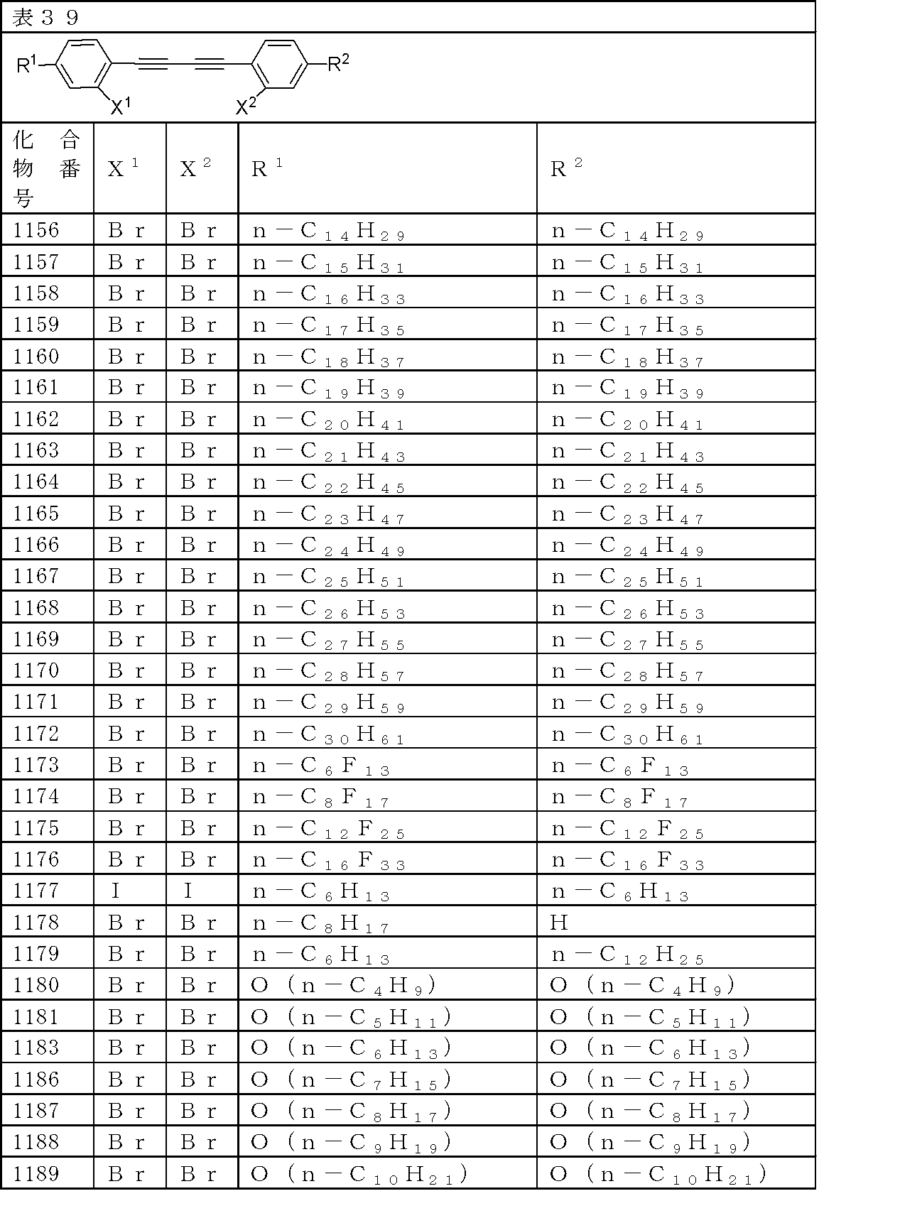
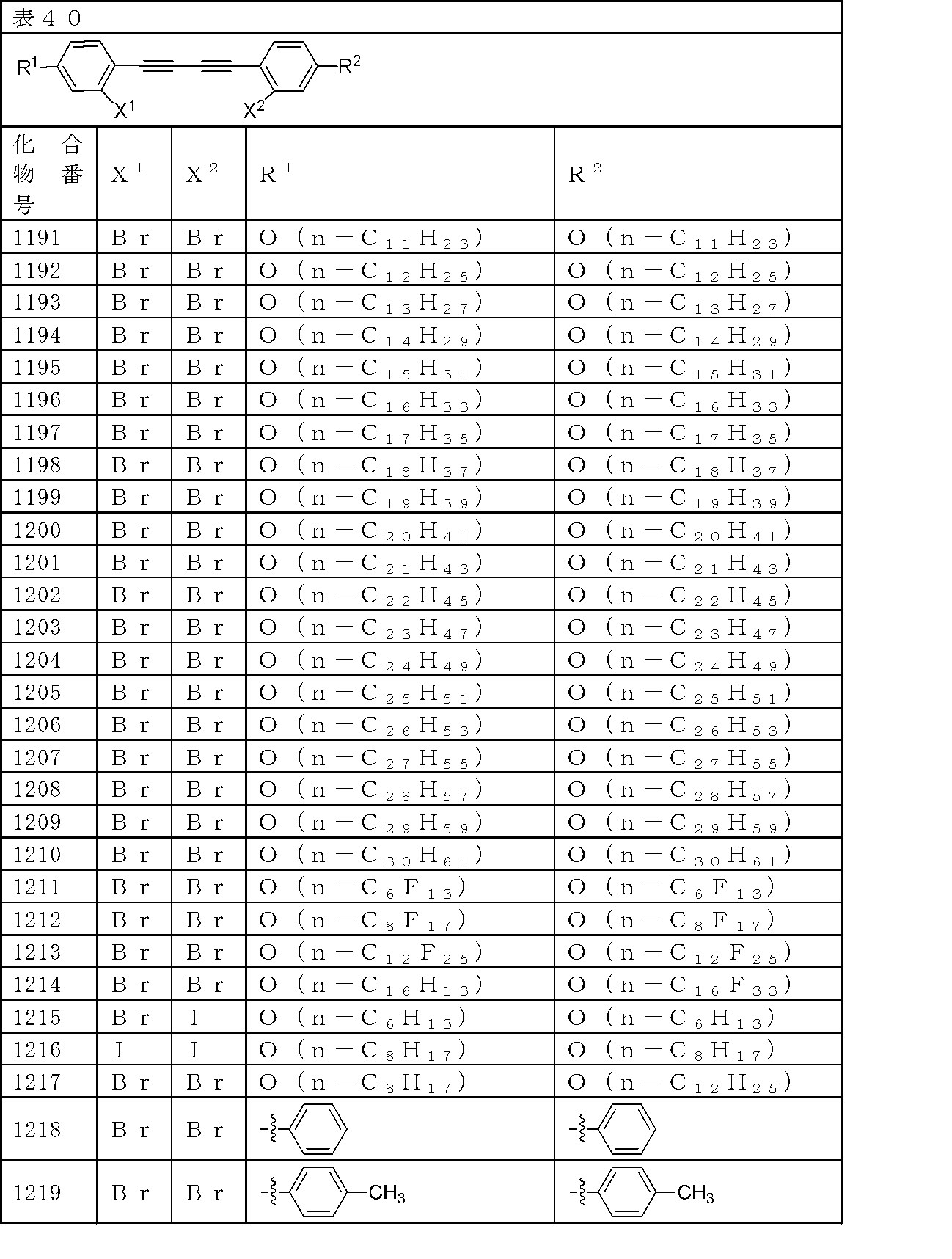
- 1,4-bis (2-bromo-4-hexylphenyl) diacetylene represented by the formula [1145] as an orange powder by recrystallization from toluene (hereinafter sometimes referred to as compound [1145]) (11.8 g, 22.0 mmol, yield 45.0%).
- N-bromosuccinimide (NBS: 53) was added to a mixed solution of 4-dodecylaniline (manufactured by Wako Pure Chemical Industries, Ltd.) (74.51 g), ammonium acetate (AcONH 4 : 2.20 g), acetonitrile (MeCN: 855 mL). .26 g) was added and stirred for 3 hours. Thereafter, the reaction solution was concentrated with an evaporator, and the residue was washed with water and brine. Ethyl acetate was added, the organic layer was extracted, dried over sodium sulfate, and concentrated with an evaporator to obtain a black oil.
- Example 3 Formation of a thin film composed of the compound [5] by vacuum deposition and production of an organic transistor having the thin film>
- An electrode was prepared by sequentially vacuum depositing 3 nm of chromium and 50 nm of gold on a substrate on which a hexamethyldisilazane film was formed by spin coating on an n-doped silicon wafer with a SiO 2 thermal oxide film, using a metal mask.
- the channel width and channel length of the prepared electrode were 2000 ⁇ m and 20 ⁇ m, respectively.
- a sample obtained by purifying the compound [5] synthesized in Example 1 by sublimation was placed in a quartz crucible, the crucible was heated, and a thin film composed of the compound [5] was formed by vacuum deposition.
- the degree of vacuum in the apparatus chamber used for the vacuum deposition method was 1 ⁇ 10 ⁇ 4 Pascal or less, and the substrate temperature was in the range of room temperature (24 ° C.) to 80 ° C.
- the film thickness of the thin film was about 200 nm.
- the organic transistor (refer FIG. 1) which has the thin film which consists of the compound [5] refine
- Example 4 Measurement of organic transistor having thin film made of compound [5]>
- the electrical characteristics of the organic transistor having a thin film made of the compound [5] prepared in Example 3 were measured under a vacuum using a parameter analyzer.
- the negative gate voltage is applied to the gate electrode (Vg)
- the negative drain current (Id) increases. Therefore, the manufactured organic transistor having a thin film made of the compound [5] is p-type. It was confirmed that this was an organic transistor.
- the change curve of the drain current (Id) with respect to the drain voltage (Vd) was good, and had a saturation region at a high drain voltage.
- L and W are the channel length and the channel width of the organic transistor, respectively
- Ci is the electrostatic capacity per unit area of the insulator layer for the gate electrode (hereinafter sometimes referred to as a gate insulating film). It is a capacity
- Vg is a gate voltage
- Vt is a threshold voltage of the gate voltage.
- the thin film made of the compound [5] produced at the substrate temperature of 60 ° C.
- the ratio of the drain current Id value when the gate voltage was 0 V and ⁇ 50 V (hereinafter sometimes referred to as on / off ratio) was 10 7 .
- Example 5 Solvent solubility of compound [5] and formation of a thin film containing compound [5] by coating film forming process>
- Compound [5] produced in Example 1 was dissolved in tetrahydrofuran to prepare a solution composition having a concentration of Compound [5] of 0.5% by weight.
- This solution composition was applied by spin coating on an n-doped silicon wafer with a SiO 2 thermal oxide film that had been subjected to hexamethyldisilazane treatment to form a thin film made of compound [5]. Further, the formed thin film was kept at 80 ° C. for 30 minutes. The thickness of the thin film was about 30 nm.
- Example 6 Production of organic transistor having thin film made of compound [5]> A source electrode and a drain electrode were formed on the thin film obtained in Example 5 by depositing molybdenum oxide and then a gold layer on the thin film by a vacuum deposition method using a metal mask.
- the channel width and the channel length of the organic TFT obtained by forming the source electrode and the drain electrode were 2000 ⁇ m and 20 ⁇ m, respectively. In this way, an organic transistor having a thin film containing the compound [5] as shown in FIG. 2 could be produced.
- Example 7 Measurement of organic transistor having thin film made of compound [5]> As a result of measuring the electrical characteristics of the organic transistor manufactured in Example 6 in the same manner as in Example 4, the field effect mobility (carrier mobility) and the on / off ratio of the carriers were 0.3 cm 2 / Vs and 10 7 , respectively. Met.
- Example 8 Preparation of a thin film composed of compound [14] and an organic transistor having the thin film>
- a source electrode and a drain electrode in the order of SiO 2 thermal oxide film, chromium and gold
- the substrate was ultrasonically cleaned with acetone for 10 minutes and then irradiated with ozone UV for 20 minutes.
- the substrate surface was silane-treated by immersing the substrate in a toluene diluted solution of phenylethyltrichlorosilane for 2 minutes.
- a transistor substrate was fabricated by modifying the Au electrode surface formed on the substrate by immersing the substrate in isopropyl alcohol diluted with perfluorobenzenethiol for 2 minutes.
- the compound [14] synthesized in Example 2 was placed in a quartz crucible, the crucible was heated, and a thin film made of the compound [14] was formed on the transistor substrate by vacuum deposition.
- the degree of vacuum in the apparatus chamber used for the vacuum deposition method was 1 ⁇ 10 ⁇ 4 Pascal or less, and the temperature of the substrate was 80 ° C.
- the film thickness of the thin film was about 100 nm.
- Example 9 Measurement of organic transistor having a thin film made of compound [14]> The transistor characteristics were measured under the condition that the drain voltage (Vd) of the organic thin film transistor element obtained in Example 8 was set to ⁇ 40V and the gate voltage Vg was changed to 20 to ⁇ 40V.
- Vd drain voltage
- Vg gate voltage
- the field effect mobility of an organic thin film transistor (mobility) is 0.4 cm 2 / Vs
- the on / off ratio was 10 7.
- Example 10 Solvent Solubility of Compound [14] and Formation of Thin Film Containing Compound [14] by Coating Film Forming Process> A 0.5 wt% dichlorobenzene solution of compound [14] was heated to 100 ° C. and applied by spin coating on the substrate obtained in the same manner as in Example 8, and dried on a hot plate at 120 ° C. for 30 minutes. Thus, a thin film of a compound having a thickness of about 30 nm was formed.
- Example 11 Measurement of organic transistor having a thin film made of compound [14]>
- the transistor characteristics of the organic thin film transistor element obtained as described above were measured under the condition that the drain voltage (Vd) was set to ⁇ 40V and the gate voltage (Vg) was changed from 20 to ⁇ 40V.
- Vd drain voltage
- Vg gate voltage
- the field effect mobility of an organic thin film transistor 0.5 cm 2 / Vs, the on / off ratio was 10 7.
- a thin film was formed by vacuum deposition in the same manner as in Example 3 except that the compound C-1 represented by the above formula disclosed in Patent Document 1 was used. Subsequently, an organic transistor having the thin film was produced. went. As a result of measuring the electrical characteristics of the obtained organic transistor according to Example 4, the carrier mobility and the on / off ratio of the obtained organic transistor were 10 ⁇ 5 cm 2 / Vs and 10 3 , respectively. .
- Example 12 Preparation of compound [41], formation of a thin film comprising compound [41] by a coating film forming method, and preparation and measurement of an organic transistor having the thin film> Except that 4-pentyloxyaniline is used in place of 4-dodecylaniline, it is the same as in Production Example 7, Production Example 8 and Example 2 to represent compound [41] (compound No. 41 in Table 2). ) Can be obtained.
- a transistor substrate is prepared in the same manner as in Example 8, and subsequently, an organic transistor having the thin film is prepared in the same manner as in Example 10.
- a high carrier mobility value can be obtained.
- Example 13 Preparation of compound [155] Compound [155] (Compound No. 155 in Table 9) was prepared in the same manner as in Production Example 7, Production Example 8 and Example 2 except that 4- (4-phenylbutyl) aniline was used instead of 4-dodecylaniline. Meaning). Using the resulting compound [155], a transistor substrate is prepared in the same manner as in Example 8, and then an organic transistor having the thin film is prepared in the same manner as in Example 10. By measuring the obtained organic transistor according to Example 9, a high carrier mobility value can be obtained.
- Example 14 Preparation of compound [222])
- Compound [218] (Compound No. 222 in Table 13) was prepared in the same manner as in Production Example 7, Production Example 8 and Example 2 except that 3-octylaniline was used instead of 4-hexylaniline in Production Example 1. Meaning).
- a transistor substrate is prepared in the same manner as in Example 8, and subsequently, an organic transistor having the thin film is prepared in the same manner as in Example 10.
- a high carrier mobility value can be obtained.
- Example 16 Preparation of compound [12]> Compound [12] (Compound No. 15 in Table 1) was prepared in the same manner as in Production Example 7, Production Example 8 and Example 2 except that 4- (2-hexyldecyl) aniline was used instead of 4-dodecylaniline. Meaning).
- Example 17 Preparation of compound [15]> Except that 4-tridecylaniline is used in place of 4-dodecylaniline, compound [15] is defined in the same manner as in Production Example 7, Production Example 8 and Example 2 (meaning compound No. 15 in Table 1). Can be obtained.
- Example 18 Preparation of compound [18]> Except that 4-hexadecylaniline is used in place of 4-dodecylaniline, Compound [18] is defined in the same manner as in Production Example 7, Production Example 8 and Example 2 (meaning the compound of Compound No. 18 in Table 2). Can be obtained.
- the present invention can provide a novel substituted benzochalcogenoacene compound, a thin film containing the compound, and an organic semiconductor device containing the thin film.
Landscapes
- Chemical & Material Sciences (AREA)
- Organic Chemistry (AREA)
- Engineering & Computer Science (AREA)
- Materials Engineering (AREA)
- Physics & Mathematics (AREA)
- Spectroscopy & Molecular Physics (AREA)
- Thin Film Transistor (AREA)
- Heterocyclic Carbon Compounds Containing A Hetero Ring Having Oxygen Or Sulfur (AREA)
- Electroluminescent Light Sources (AREA)
Abstract
Description

すなわち本発明は
<1> 式(1)

で表される置換ベンゾカルコゲノアセン化合物;
<3> 式(1)におけるR1及びR2は、それぞれ独立に、水素原子、フッ素原子を有していてもよい炭素数4~30のアルキル基、フッ素原子を有していてもよい炭素数4~30のアルコキシ基、アルキル基又はアルコキシ基を有していてもよい炭素数6~30のアリール基(該アリール基はフッ素原子を有していてもよい)、フッ素原子を有していてもよい炭素数7~30のアラルキル基、アルキル基又はアルコキシ基を有していてもよい炭素数4~30のヘテロアリール基(該ヘテロアリール基はフッ素原子を有していてもよい)、フッ素原子を有していてもよい炭素数5~30のヘテロアラルキル基である<1>又は<2>記載の化合物;
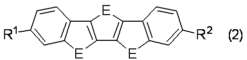
で表される<1>~<3>のいずれか記載の化合物;
<5> 式(2)において、Eはそれぞれ独立に、硫黄またはセレン原子を表す。R1及びR2はそれぞれ独立に、水素原子、フッ素原子を置換基として有していてもよい炭素数4~30のアルキル基又はフッ素原子を置換基として有していてもよい炭素数3~30のトリアルキルシリル基である<4>記載の化合物;
<6> 式(2)において、R1及びR2は、それぞれ独立に、炭素数4~30のアルキル基又は炭素数3~30のトリアルキルシリル基である<5>記載の化合物;
<7> 式(2)において、R1及びR2が炭素数4~30のアルキル基である<5>記載の化合物;
<8> 式(2)において、R1及びR2は、同一であり、かつ、炭素数4~20のアルキル基である<5>記載の化合物;
<9> 式(2)において、R1及びR2が炭素数6~12のアルキル基である<5>記載の化合物;
<10> 式(2)におけるR1及びR2は、それぞれ独立に、水素原子、フッ素原子を有していてもよい炭素数4~30のアルキル基、フッ素原子を有していてもよい炭素数4~30のアルコキシ基、アルキル基を有していてもよい炭素数6~30のアリール基(該アリール基はフッ素原子を有していてもよい)、フッ素原子を有していてもよい炭素数7~30のアラルキル基である<4>記載の化合物;
<11> 式(2)において、R1及びR2は、同一であり、かつ、炭素数4~20のアルコキシ基である<4>記載の化合物;
<12> 式(2)において、R1及びR2は、同一であり、かつ、炭素数1~20のアルキル基を有する炭素数6~10のアリール基である<4>記載の化合物;
<13> 式(2)において、R1及びR2は、同一であり、かつ、炭素数7~20のアラルキル基である<4>記載の化合物;
<14> 式(2)において、R1及びR2はそれぞれ独立に、炭素数3~30のトリアルキルシリル基である<5>記載の化合物;
<15> 式(2)において、R1及びR2はそれぞれ独立に、炭素数3~14のトリアルキルシリル基である<5>記載の化合物;
<16> 式(2)において、R1及びR2は同一であり、ヘキシル基又はドデシル基である<4>又は<5>記載の化合物;
<17> 式(2)において、Eが、全て硫黄原子である<4>~<16>のいずれか記載の化合物;
<19> 式(2)において、Eが、全て硫黄原子であり、R1及びR2はドデシル基である<4>記載の化合物;
<20> 式(2)において、Eが、全て硫黄原子であり、R1及びR2はそれぞれ独立に、炭素数6~12のアルキル基である請求項4記載の化合物;
<21> 下記式[5]、[7]、[12]、[14]、[15]、[18]又は[42]で示される化合物。
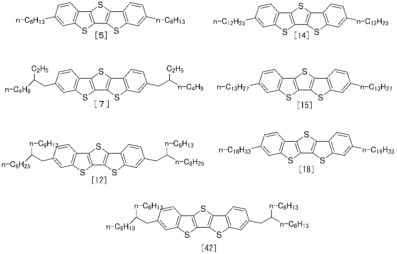
式(1)で表される化合物が、式(3)
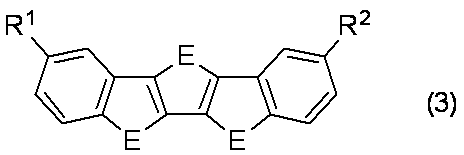
で表される<1>~<3>のいずれか記載の化合物;
<23> 式(3)において、R1及びR2は、同一であり、かつ、炭素数4~20のアルキル基である<22>記載の化合物;
<25> <1>~<23>のいずれか記載の化合物からなる薄膜;
<26> <24>又は<25>記載の薄膜を含有する有機半導体デバイス;
<27> <24>又は<25>記載の薄膜を含有する有機トランジスタ;
等である。
式(1)、(2)および(3)中、Eはそれぞれ独立に、硫黄またはセレン原子を表す。R1及びR2は、それぞれ独立に、水素原子、置換基を有していてもよい炭素数4~30のアルキル基、置換基を有していてもよい炭素数4~30のアルコキシ基、置換基を有していてもよい炭素数6~30のアリール基、置換基を有していてもよい炭素数7~30のアラルキル基、置換基を有していてもよい炭素数4~30のヘテロアリール基、置換基を有していてもよい炭素数5~30のヘテロアラルキル基、フッ素原子を有していてもよい炭素数3~30のトリアルキルシリル基を表す。但し、R1及びR2の少なくとも一方は水素原子ではない。
ハロゲン原子としては、フッ素原子、塩素原子、臭素原子などが挙げられる。
炭素数1~30のアルコキシ基としては、メトキシ基、エトキシ基、n-プロポキシ基、n-ブトキシ基、n-ペンチルオキシ基、n-ヘキシルオキシ基、n-ヘプチルオキシ基、n-オクチルオキシ基、n-ノニルオキシ基、n-デシルオキシ基、n-ウンデシルオキシ基、n-ドデシルオキシ基、n-トリデシルオキシ基、n-テトラデシルオキシ基、n-ペンタデシルオキシ基、n-ヘキサデシルオキシ基、n-ヘプタデシルオキシ基、n-オクタデシルオキシ基、n-ノナデシルオキシ基、n-イコシルオキシ基、n-ヘンイコシルオキシ基、n-ドコシルオキシ基、n-トリコシルオキシ基、n-テトラコシルオキシ基、n-ペンタコシルオキシ基、n-ヘキサコシルオキシ基、n-ヘプタコシルオキシ基、n-オクタコシルオキシ基、n-ノナコシルオキシ基、n-トリアコンチルオキシ基などが挙げられる。
好ましくは、n-ブトキシ基、n-ペンチルオキシ基、n-ヘキシルオキシ基、n-ヘプチルオキシ基、n-オクチルオキシ基、n-ノニルオキシ基、n-デシルオキシ基、n-ウンデシルオキシ基、n-ドデシルオキシ基、n-トリデシルオキシ基、n-テトラデシルオキシ基、n-ペンタデシルオキシ基、n-ヘキサデシルオキシ基、n-ヘプタデシルオキシ基、n-オクタデシルオキシ基、n-ノナデシルオキシ基、n-イコシルオキシ基等の炭素数4~20のアルコキシ基が挙げられる。
アリール基としては、フェニル基、1-ナフチル基、2-ナフチル基等を挙げることができる。
アラルキル基としては、下記式で表される基が挙げられる。

ヘテロアリール基とは、アリール基の芳香環に含まれる炭素原子の少なくとも1つが、窒素原子、酸素原子、硫黄原子、セレン原子などの複素原子に置き換えられた基を意味し、例えば、チエニル基、フリル基、チアゾリル基、チエノ[3,2-b]チエニル基、フロロ[3,2-b]フリル基、チエノ[3,2-b]フリル基、ベンゾ[b]チエニル基、ベンゾ[b]フリル基等が挙げられる。ヘテロアリール基としては、チエニル基、チアゾリル基、チエノ[3,2-b]チエニル基、ベンゾ[b]チエニル基、ベンゾ[b]フリル基が好ましい。
ヘテロアラルキル基とは、アラルキル基の芳香環に含まれる炭素原子の少なくとも1つが、窒素原子、酸素原子、硫黄原子、セレン原子などの複素原子に置き換えられた基を意味し、ヘテロアラルキル基としては、例えば、下記式で表される基を挙げることができる。

さらに好ましくは、下記式を挙げることができる。

置換基を有する炭素数4~30のアルコキシ基としては、例えば、パーフルオロヘキシルオキシ基、パーフルオロオクチルオキシ基、パーフルオロデシルオキシ基、パーフルオロドデシルオキシ基、パーフルオロトリデシルオキシ基、、メトキシエトキシエトキシ基等が挙げられる。
「置換基を有していてもよいアリール基」としては、例えば、フェニル基、1-ナフチル基、2-ナフチル基、パーフルオロフェニル基、4-ヘキシルフェニル基、4-ヘキシルオキシフェニル基等を挙げることができる。
「置換基を有していてもよい炭素数7~30のアラルキル基」の置換基としては、フッ素原子が好ましい。
「置換基を有していてもよい炭素数7~30のアラルキル基」としては、例えば、下記式

下記式


「置換基を有していてもよいヘテロアリール基」としては、2-チエニル基、2-チエノ[3,2-b]チエニル基、2-ベンゾ[b]チエニル基、5-フルオロ-2-チエニル基、5-ヘキシル-2-チエニル、4-ヘキシルオキシ-2-チエニル基等を挙げることができる。
「置換基を有していてもよい炭素数5~30のヘテロアラルキル基」の置換基としては、フッ素原子が好ましい。
「置換基を有していてもよい炭素数5~30のヘテロアラルキル基」としては、例えば、下記式で表される基を挙げることができる。

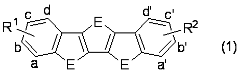
R1はaに、R2はa’に結合位置がある場合、R1はbに、R2はb’に結合位置がある場合、R1はcに、R2はc’に結合位置がある場合、R1はdに、R2はd’に結合位置がある場合を挙げることができる。好ましくは、R1はbに、R2はb’に結合位置がある場合、すなわち、式(2)

で表される化合物、または、R1はcに、R2はc’に結合位置がある場合、すなわち、式(3)
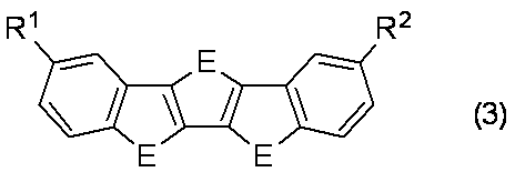
で表される化合物を挙げることができる。
Eが、全て硫黄原子である式(1)で示される化合物;
3つのEのうち、2つが硫黄原子であり、1つがセレン原子である式(1)で示される化合物;
Eはそれぞれ独立に、硫黄またはセレン原子を表し、R1及びR2は、それぞれ独立に、水素原子、フッ素原子を有していてもよい炭素数4~30のアルキル基、フッ素原子を有していてもよい炭素数4~30のアルコキシ基、アルキル基又はアルコキシ基を有していてもよい炭素数6~30のアリール基(該アリール基はフッ素原子を有していてもよい)、フッ素原子を有していてもよい炭素数7~30のアラルキル基、アルキル基又はアルコキシ基を有していてもよい炭素数4~30のヘテロアリール基(該ヘテロアリール基はフッ素原子を有していてもよい)、フッ素原子を有していてもよい炭素数5~30のヘテロアラルキル基である(但し、R1及びR2の少なくとも何れか一方は、水素原子でない)式(1)で示される化合物;
R1及びR2は、それぞれ独立に、フッ素原子を有していてもよい炭素数4~30のアルキル基、フッ素原子を有していてもよい炭素数4~30のアルコキシ基、アルキル基又アルコキシ基を有していてもよい炭素数6~30のアリール基(該アリール基はフッ素原子を有していてもよい)である式(1)で示される化合物;
R1及びR2は、それぞれ独立に、炭素数4~30のアルキル基又は炭素数3~30のトリアルキルシリル基である式(1)で示される化合物;
R1及びR2が炭素数4~30のアルキル基である式(1)で示される化合物;
R1及びR2は、同一であり、かつ、炭素数4~20のアルキル基である式(1)で示される化合物;
R1及びR2が、それぞれ独立に、炭素数6~12のアルキル基である式(1)で示される化合物;
R1及びR2は、同一であり、かつ、炭素数4~20のアルコキシ基である式(1)で示される化合物;
R1及びR2は、同一であり、かつ、炭素数4~20のアルキル基を有する炭素数6~10のアリール基である式(1)で示される化合物;
R1及びR2は、同一であり、かつ、炭素数7~20のアラルキル基である式(1)で示される化合物;
R1及びR2は、それぞれ独立に、炭素数3~30のトリアルキルシリル基である式(1)で示される化合物;
R1及びR2はそれぞれ独立に、炭素数3~14のトリアルキルシリル基である式(1)で示される化合物;
R1及びR2は同一であり、ヘキシル基又はドデシル基である式(1)で示される化合物;
Eはそれぞれ独立に、硫黄またはセレン原子を表し、R1及びR2は、それぞれ独立に、水素原子、炭素数4~30のアルキル基、炭素数4~30のアルコキシ基、アルキル基又はアルコキシ基を有していてもよい炭素数6~30のアリール基、フッ素原子を有していてもよい炭素数7~30のアラルキル基、アルキル基又はアルコキシ基を有していてもよい炭素数4~30のヘテロアリール基(該アリール基はフッ素原子を有していてもよい)、フッ素原子を有していてもよい炭素数5~30のヘテロアラルキル基である(但し、R1及びR2の少なくとも何れか一方は、水素原子でない)式(2)で示される化合物;
Eはそれぞれ独立に、硫黄またはセレン原子を表し、R1及びR2はそれぞれ独立に、水素原子、フッ素原子を置換基として有していてもよい炭素数4~30のアルキル基又はフッ素原子を置換基として有していてもよい炭素数3~30のトリアルキルシリル基である式(2)で示される化合物;
Eが、全て硫黄原子である式(2)で示される化合物;
3つのEのうち、2つが硫黄原子であり、1つがセレン原子である式(1)で示される化合物;
R1及びR2は、それぞれ独立に、炭素数4~30のアルキル基又は炭素数3~30のトリアルキルシリル基である式(2)で示される化合物;
R1及びR2が炭素数4~30のアルキル基である式(2)で示される化合物;
R1及びR2は、同一であり、かつ、炭素数4~20のアルキル基である式(2)で示される化合物;
R1及びR2が炭素数6~12のアルキル基である式(2)で示される化合物;
Eが、全て硫黄原子であり、R1及びR2がそれぞれ独立に、炭素数6~12のアルキル基である式(2)で示される化合物;
R1及びR2は、同一であり、かつ、炭素数4~20のアルコキシ基である式(2)で示される化合物;
R1及びR2は、同一であり、かつ、炭素数1~20のアルキル基を有する炭素数6~10のアリール基である式(2)で示される化合物;
R1及びR2は、同一であり、かつ、炭素数7~20のアラルキル基である式(2)で示される化合物;
R1及びR2はそれぞれ独立に、炭素数3~30のトリアルキルシリル基である式(2)で示される化合物;
R1及びR2はそれぞれ独立に、炭素数3~14のトリアルキルシリル基である式(2)で示される化合物;
R1及びR2は同一であり、ヘキシル基又はドデシル基である式(2)で示される化合物;
Eが、全て硫黄原子であり、R1及びR2は、ヘキシル基である式(2)で示される化合物;
Eが、全て硫黄原子であり、R1及びR2は、ドデシル基である式(2)で示される化合物;
R1及びR2は、同一であり、かつ、炭素数4~20のアルキル基である式(3)で示される化合物。


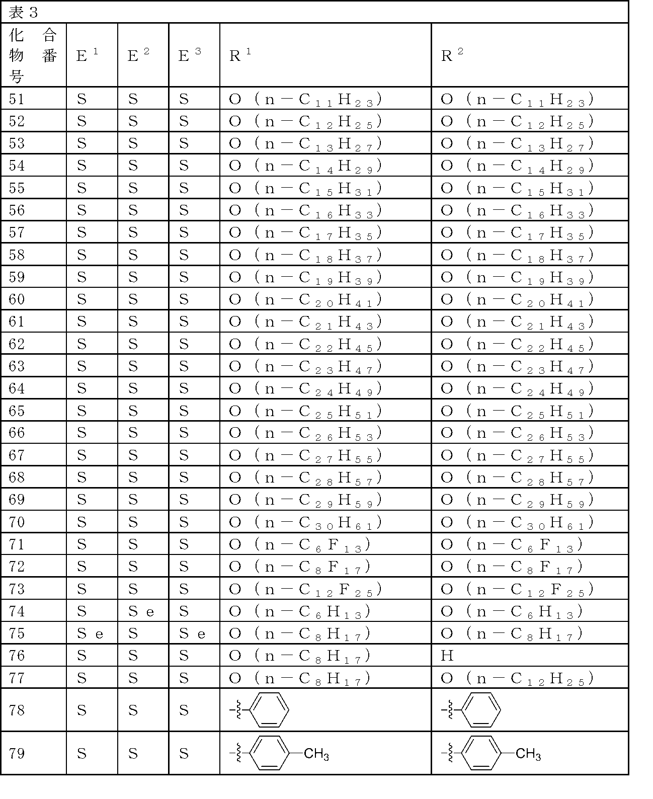





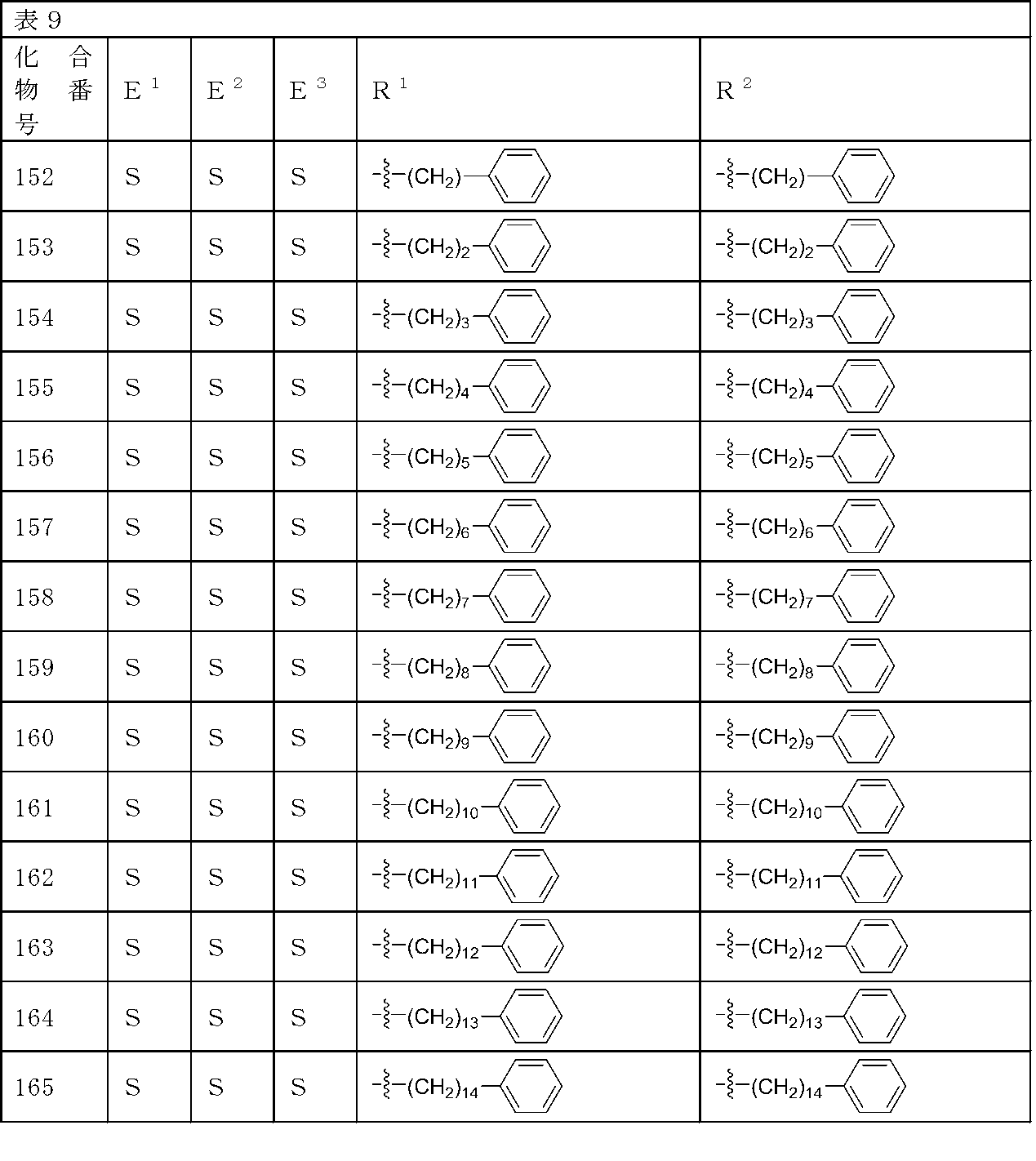


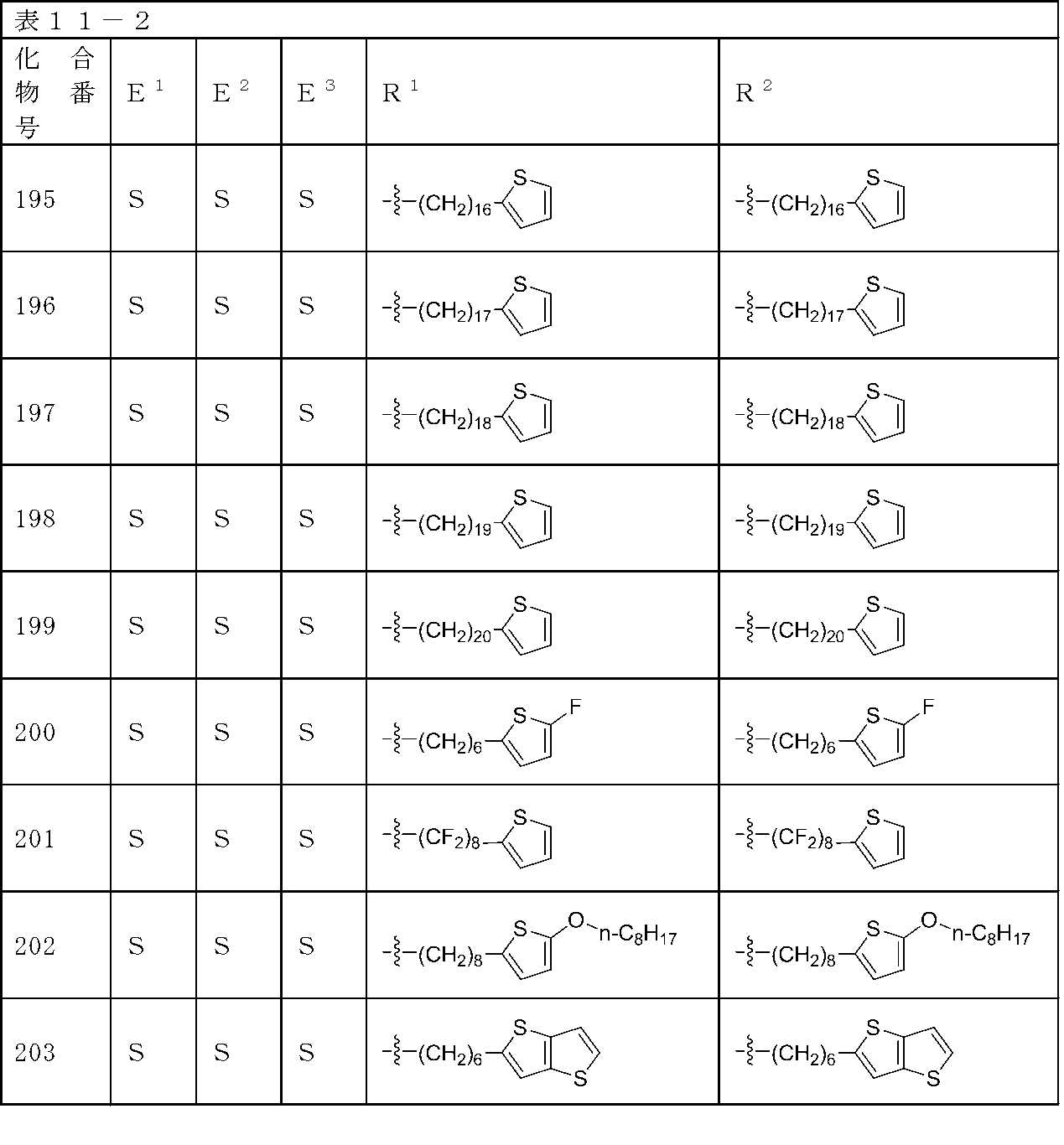

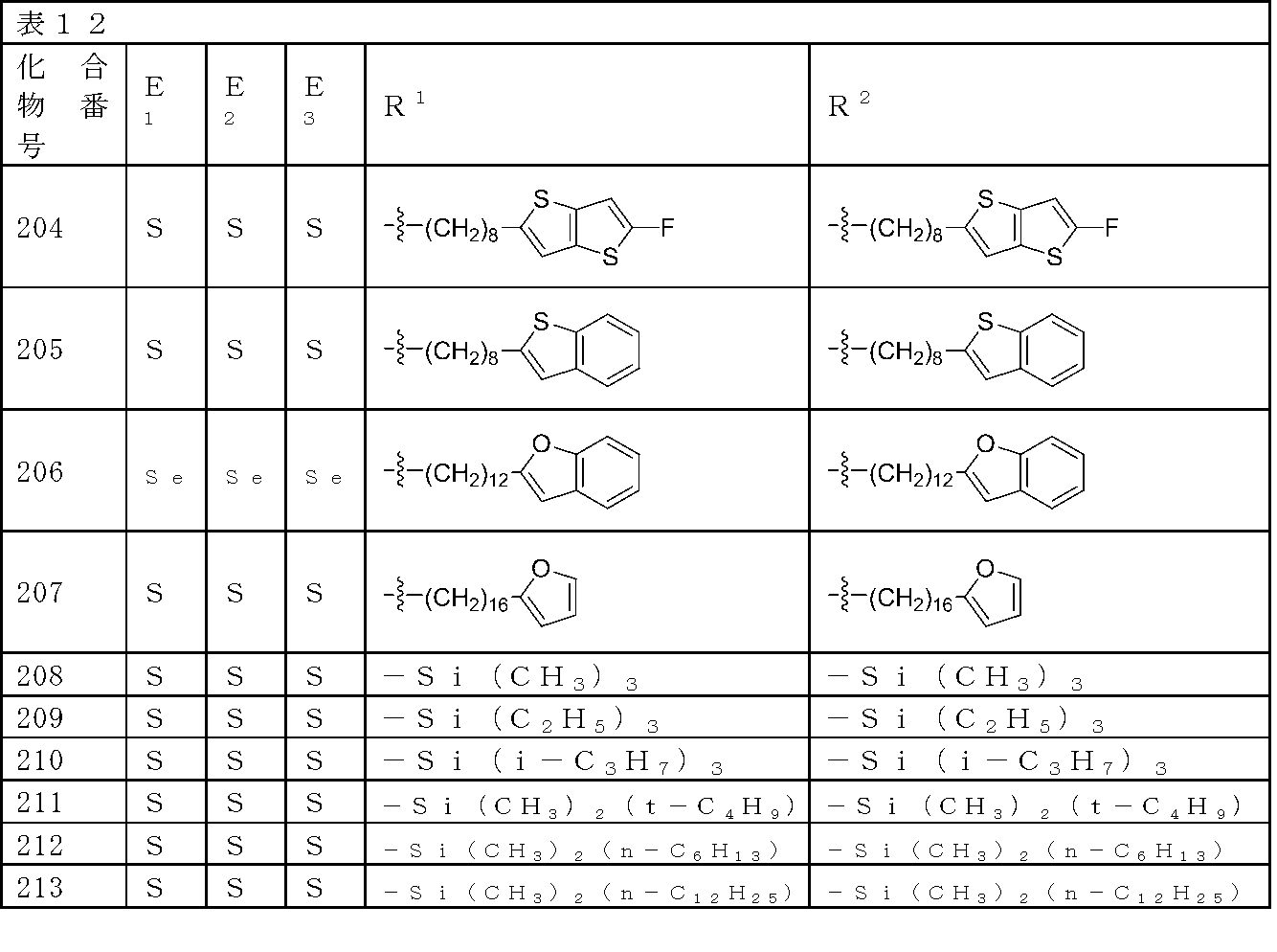

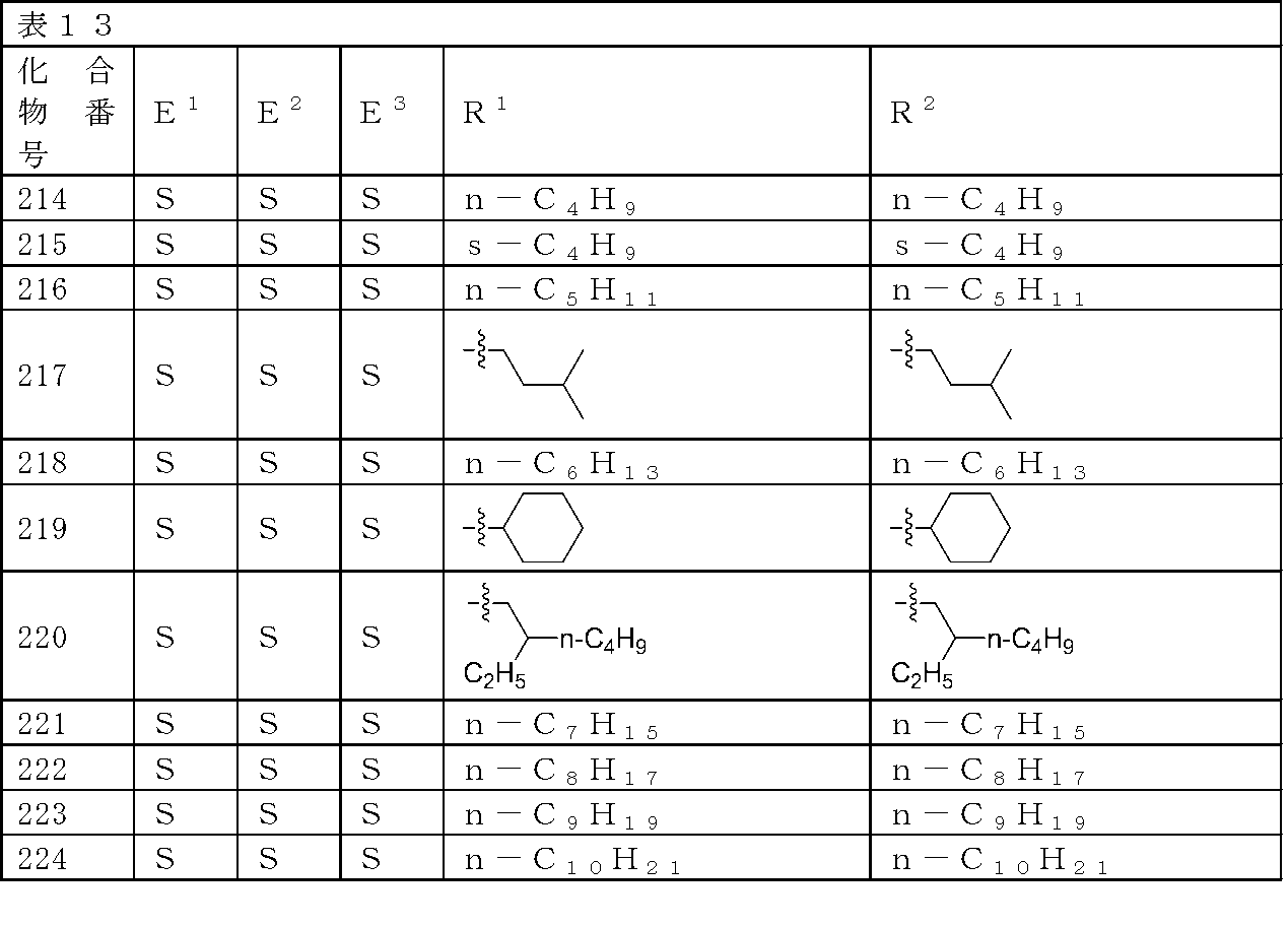




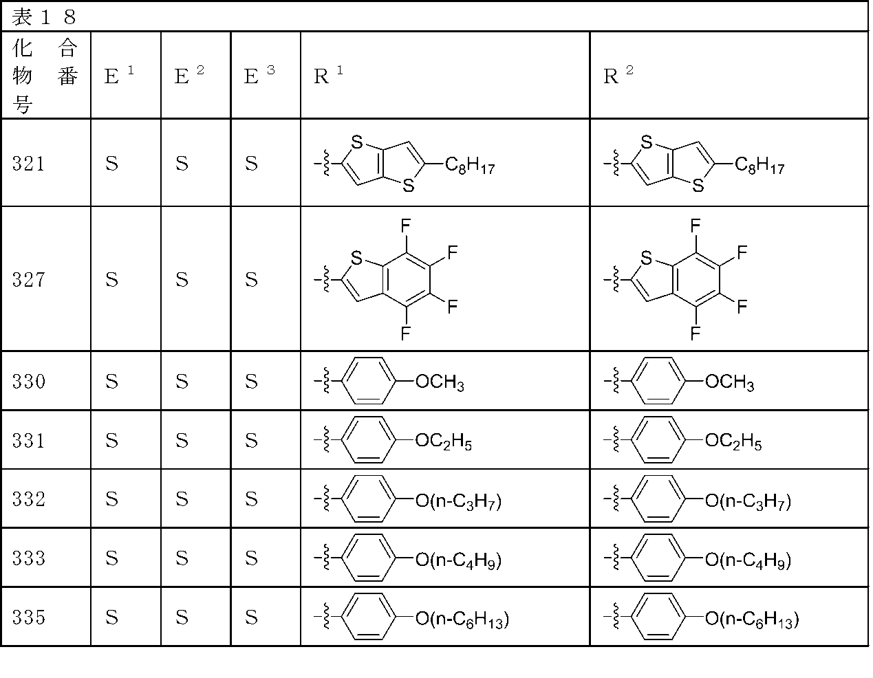


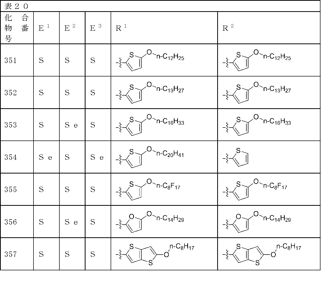

波線は結合手を意味する。

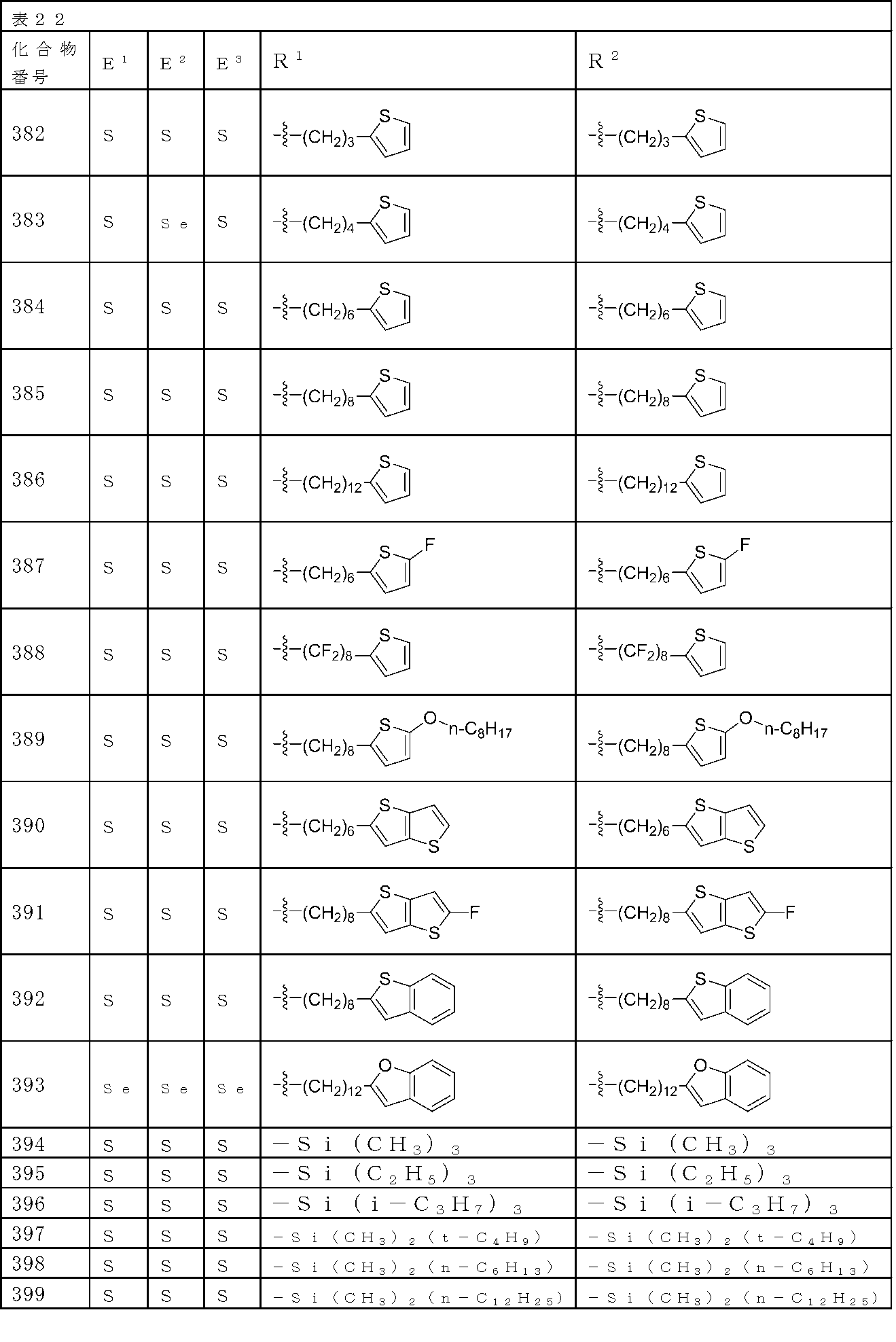

波線は結合手を意味する。











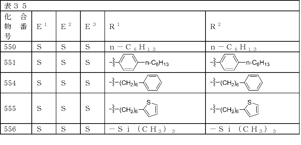
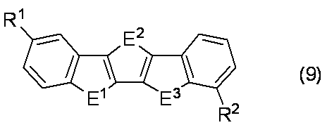

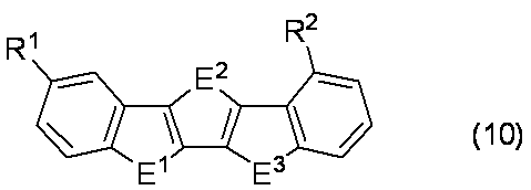
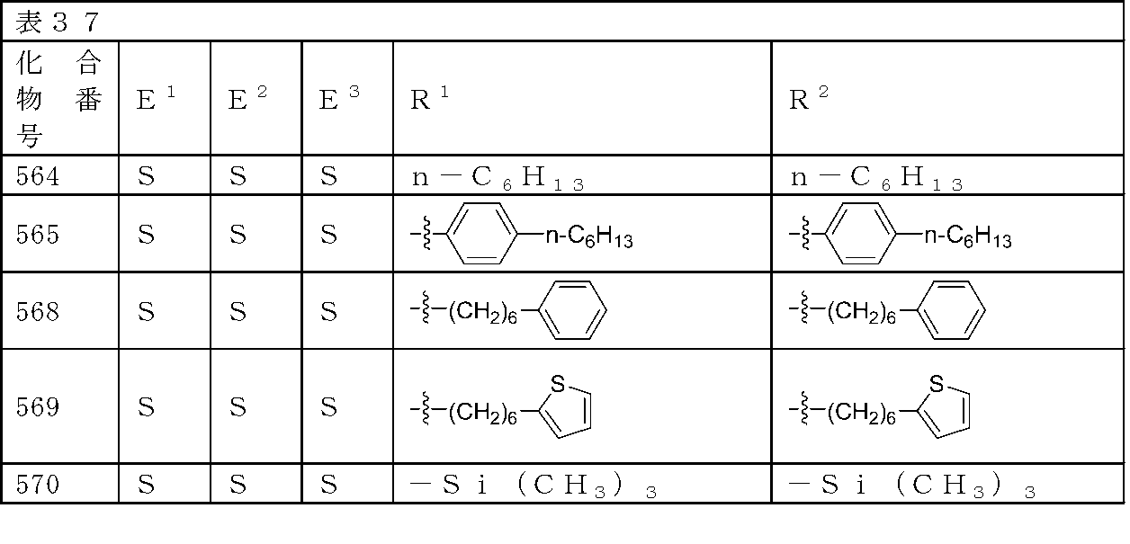
とりわけ、表中の番号が以下の置換ベンゾカルコゲノアセン化合物(1)が好ましい。
1、3、4、5、6、7、8、9、10、11、12、13、14、15、16、17、18、19、20、21、22、33、34、35、38、39、40、41、42、43、44、46、47、48、49、51、52、53、54、55、56、57、58、59、60、76、77、78、79、80、81、82、84、86、87、89、90、91、94、95、96、97、99、100、102、103、104、105、106、108、117、118、119、120、122、124、125、127、128、129、131、132、133、135、136、138、139、142、144、152、153、154、155、156、157、158、159、160、161、162、163、164、165、166、167、168、169、170、176、180、181、182、183、184、185、186、187、188、189、202、203、204、205、206、208、209、210、211、212、213、214、215、216、217、218、219、220、221、222、223、224、225、226、227、228、229、230、231、232、233、234、235、246、247、248、252、253、254、256、259、260、261、262、264、265、266、267、268、269、270、271、272、273、284、285、286、291、292、293、294、295、297、299、300、302、306、307、308、309、310、312、313、315、316、317、319、321、327、330、331、332、333、335、337、338、340、341、342、344、345、346、348、349、351、352、353、354、357、365、366、367、368、369、370、371、372、373、374、375、379、380、381、382、383、384、385、386、387、388、389、390、391、392、393、394、395、396、397、398、399
1、3、4、5、6、7、8、9、10、11、12、15、16、17、18、38、39、40、41、42、43、46、47、48、49、51、52、53、54、55、56、76、78、80、81、82、84、86、87、89、90、91、95、96、97、99、100、102、103、108、118、119、120、122、124、125、127、128、129、132、133、135、136、138、139、144、152、153、154、155、156、157、158、159、160、161、176、180、181、182、183、184、185、186、187、188、189、202、203、205、206、208、209、211、214、215、216、217、218、219、220、221、222、223、224、225、226、227、228、229、230、231、252、253、254、256、259、260、261、262、264、265、266、267、268、269、291、293、294、295、297、299、300、302、308、309、310、312、313、315、316、317、321、327、330、331、332、333、335、337、338、340、341、344、345、346、348、349、351、352、353、354、357、365、366、367、368、369、370、371、380、381、382、383、384、385、386、389、390、392、394、395、396、397が挙げられる。
また、置換ベンゾカルコゲノアセン化合物(1)を有機溶媒に溶解して、塗布及び乾燥して薄膜を形成させることができる。置換ベンゾカルコゲノアセン化合物(1)は、かかる溶媒溶解性に優れているので、後述する塗布成膜加工により容易に薄膜を形成できる
さらに、置換ベンゾカルコゲノアセン化合物(1)は、後述するように、高いキャリア移動度を示す薄膜が提供可能である。
該製造方法としては、例えば、式(5-1)
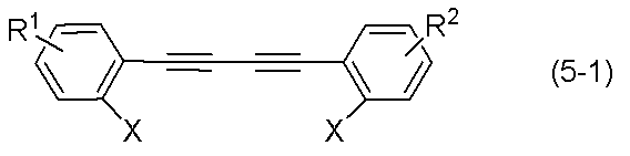
で表されるジアセチレン化合物(以下、化合物(5-1)と記すことがある)を得、次いで、有機金属塩基を用いたハロゲン-メタル交換反応によりジメタル化した(以下、この反応を「本第1反応」という。)後、硫黄又はセレンを作用させることにより、式(4-1)
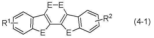
ジカルコゲンイン化合物(化合物(4-1)と記すことがある)を得(以下、この反応を「本第2反応」という。)、
次いで、得られた化合物(4-1)と、ビスシクロオクタジエニル白金(Pt(COD)2)などの白金化合物又は銅粉末などの銅化合物と、を無溶媒で加熱する方法(以下、「第3-1反応」と記すことがある)、
また、同様にして得られる化合物(4-1)と、ビスシクロオクタジエニルニッケル(Ni(COD)2)などのニッケル化合物とホスフィン化合物とを、溶媒の存在下で加熱攪拌する方法(以下、「第3-2反応」と記すことがある)、
等を挙げることができる。
有機金属塩基の使用量としては、化合物(5-1)1モルに対し、例えば、4~20モルの範囲を挙げることができ(ハロゲン原子に対して2~10倍当量の範囲)、好ましくは6~14モルの範囲(ハロゲン原子に対して3~7倍当量の範囲)、さらに好ましくは7~10モルの範囲(ハロゲン原子に対して3.5~5倍当量の範囲)が挙げられる。有機金属塩基の使用量が4モル以上であると、未反応の化合物(5-1)が低減されて、得られる化合物(4-1)の収率が向上する傾向がある。該使用量が、20モル以下であると副反応の進行が抑制され、化合物(4-1)の精製が容易になる傾向がある。
使用される溶媒としては、本第1反応及び本第2反応の進行を著しく妨げないものから選ばれ、例えば、ペンタン、ヘキサン及びヘプタンなどの脂肪族炭化水素類、ベンゼン、トルエン及びキシレンなどの芳香族炭化水素溶媒、ジエチルエーテル及びテトラヒドロフラン(THF)などのエーテル溶媒又はこれらから選ばれる2種以上の混合溶媒が用いられる。好ましい溶媒はエーテル溶媒である。
本第3-1反応の反応温度は、例えば、150~400℃の範囲を挙げることができ、好ましくは200~370℃の範囲が挙げられる。本第3-1反応の反応時間は1時間以内であり、好ましくは30分以内である。反応終了後、室温まで冷却し、例えば、クロロホルム、ジクロロメタンなどの、置換ベンゾカルコゲノアセン化合物(1)を溶解し得る溶媒を用いて、不溶不純物を濾別し、濾液を濃縮した後、必要に応じてカラムクロマトグラフィー、再結晶等の操作を行なうことで、置換ベンゾカルコゲノアセン化合物(1)が得られる。
ニッケル化合物の使用量としては、化合物(4-1)1モルに対し、例えば、0.5~5モルの範囲を挙げることができ、好ましくは0.7~3モルの範囲である。
ホスフィン化合物としては、例えば、トリフェニルホスフィン、トリシクロヘキシルホスフィン、トリ(o-トリル)ホスフィン、トリメチルホスフィン、トリ-t-ブチルホスフィン、1,2-(ジフェニルホスフィノ)エタン、1,3-(ジフェニルホスフィノ)プロパン、1,4-(ジフェニルホスフィノ)ブタン及び1,1-ビス(ジフェニルホスフィノ)フェロセンなどが挙げられ、トリフェニルホスフィンが好ましい。
ホスフィン化合物の使用量としては、ニッケル化合物1モルに対し、例えば、ホスフィン化合物が0.5~20モルの範囲等を挙げることができ、好ましくは、0.7~10モルの範囲が挙げられる。
本第3-2反応の反応温度としては、例えば、10℃から溶媒の沸点以下の範囲、を挙げることができる。
本第3-2反応の反応時間は反応温度にも拠るが、72時間以内が好ましい。
本第3-2反応の反応終了後、必要に応じて加熱しながら濾過を行って不溶不純物を除去した後、濾液を濃縮し、必要に応じてカラムクロマトグラフィー、再結晶などの精製操作を行なうことで目的化合物である置換ベンゾカルコゲノアセン化合物(1)を得ることができる。

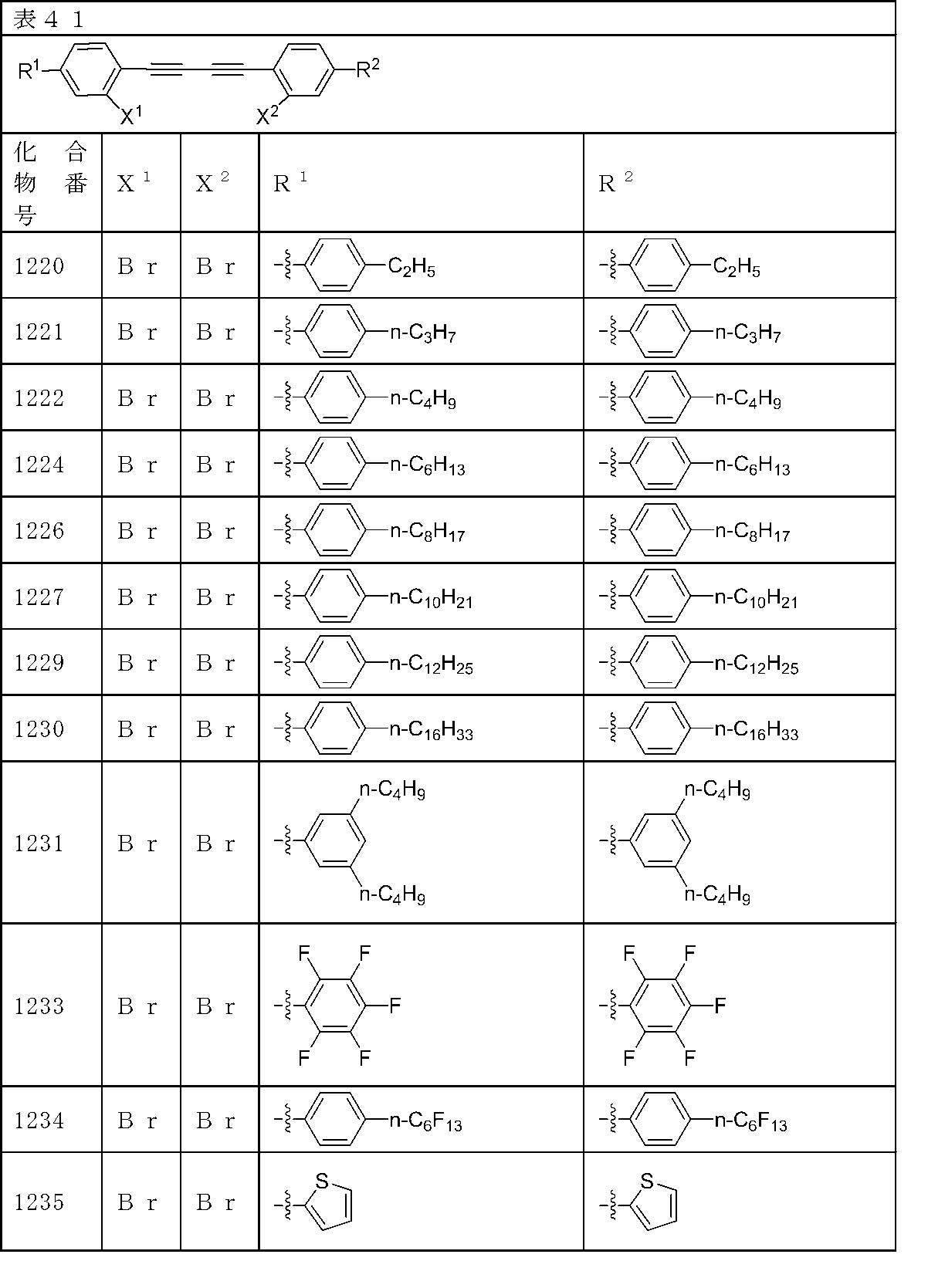


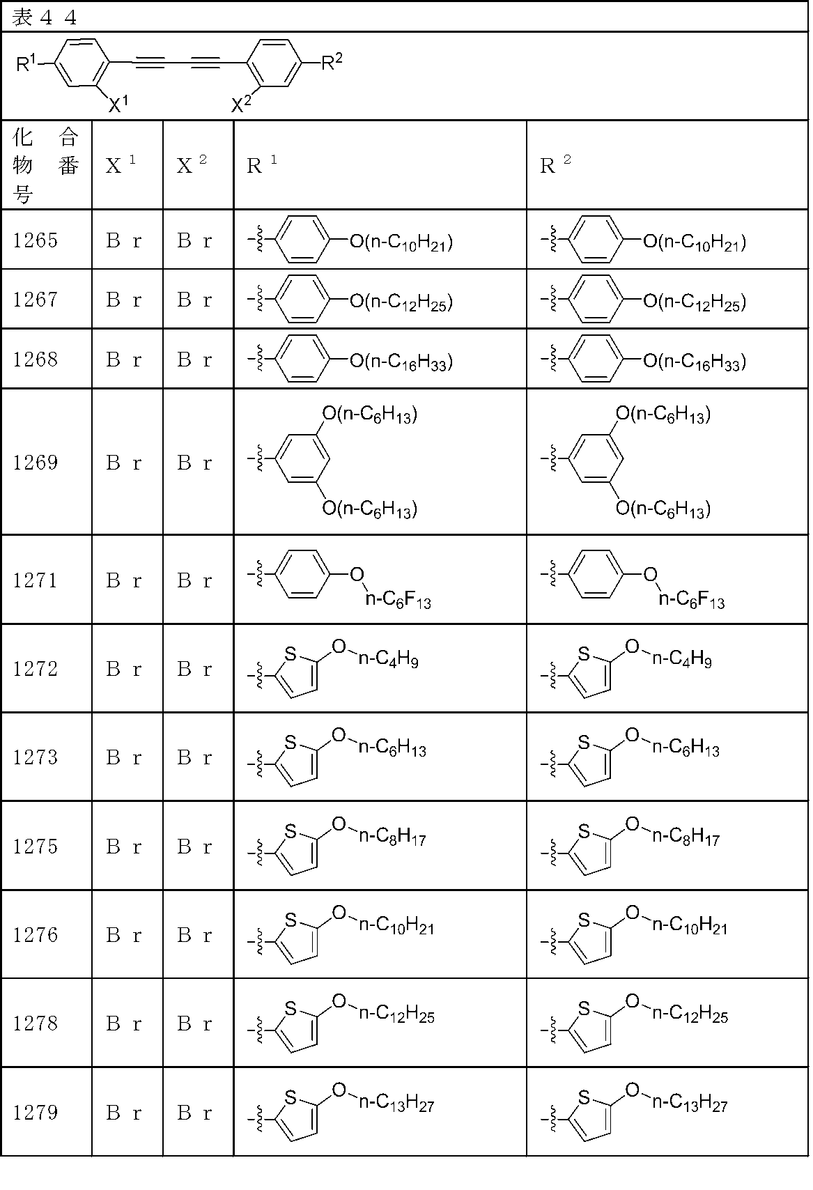
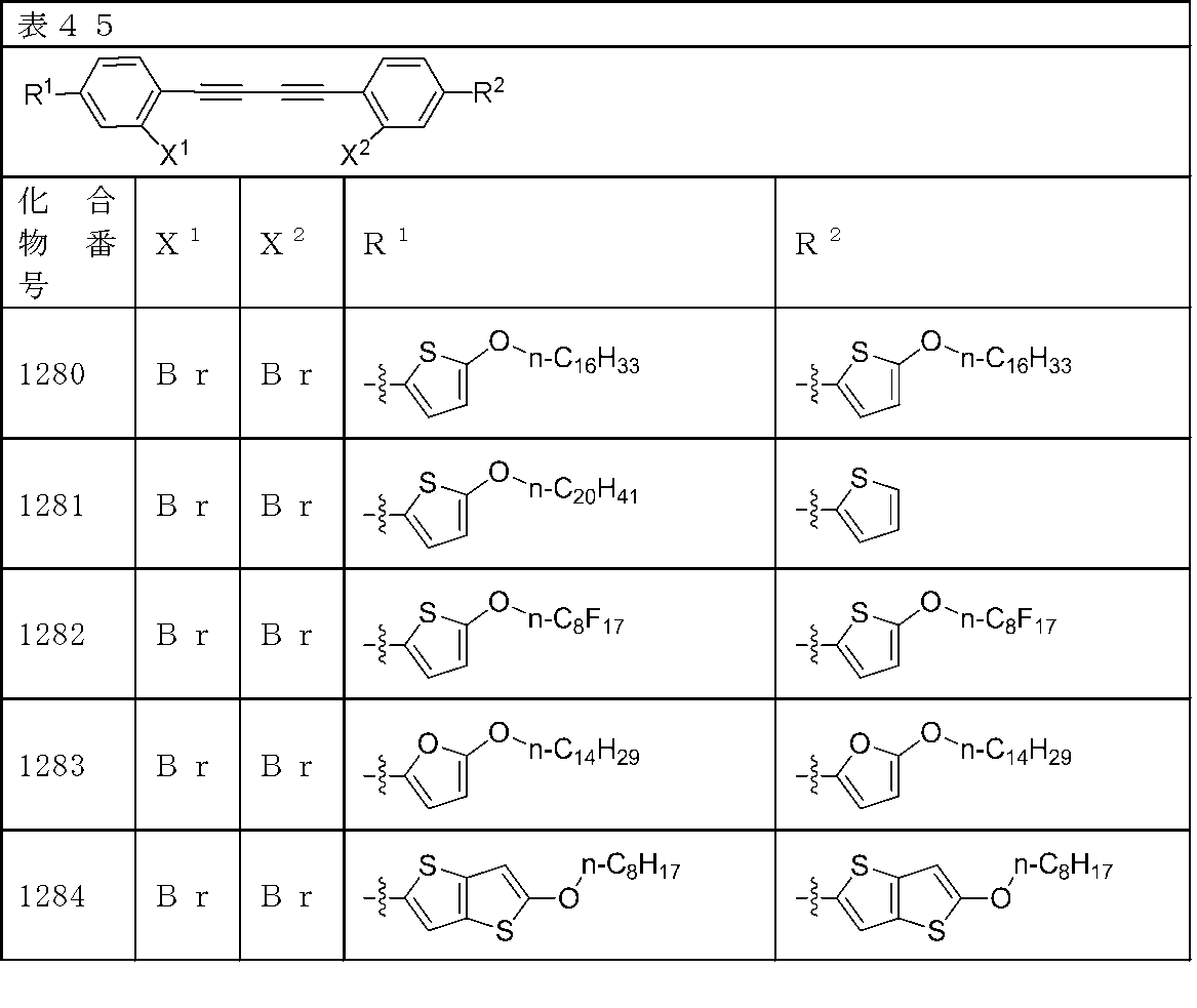


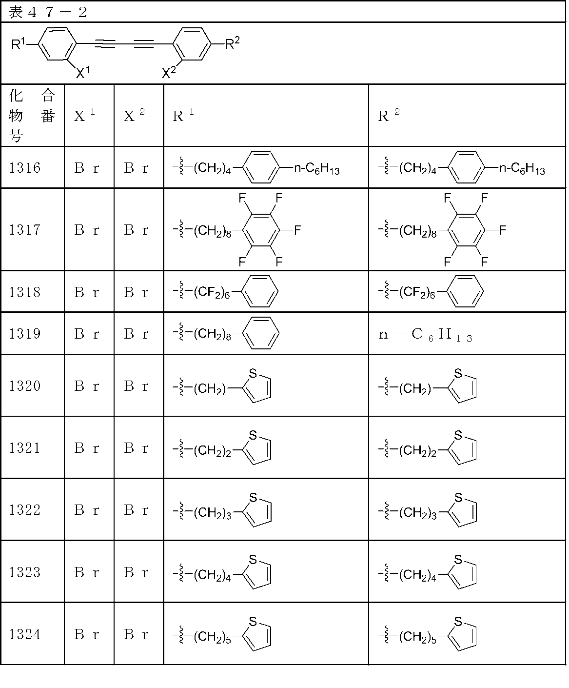


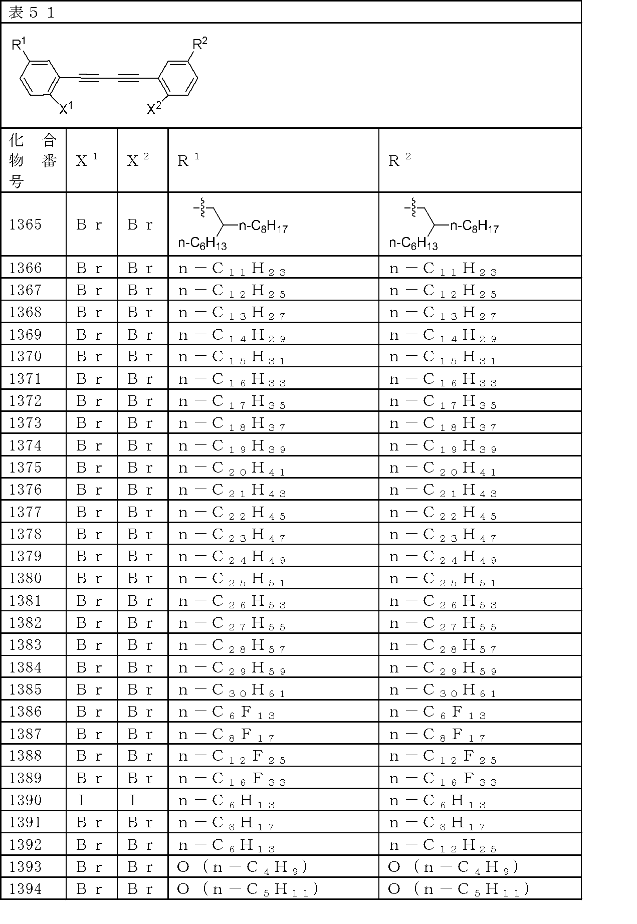

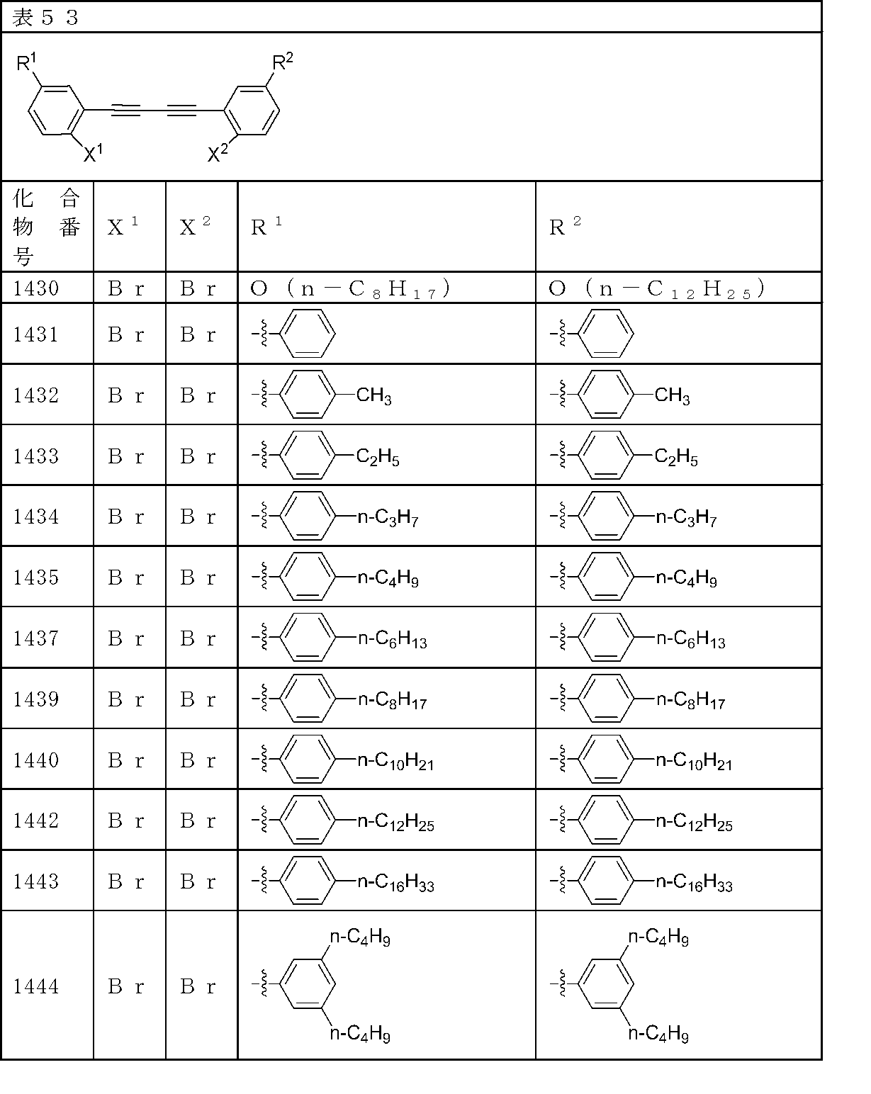
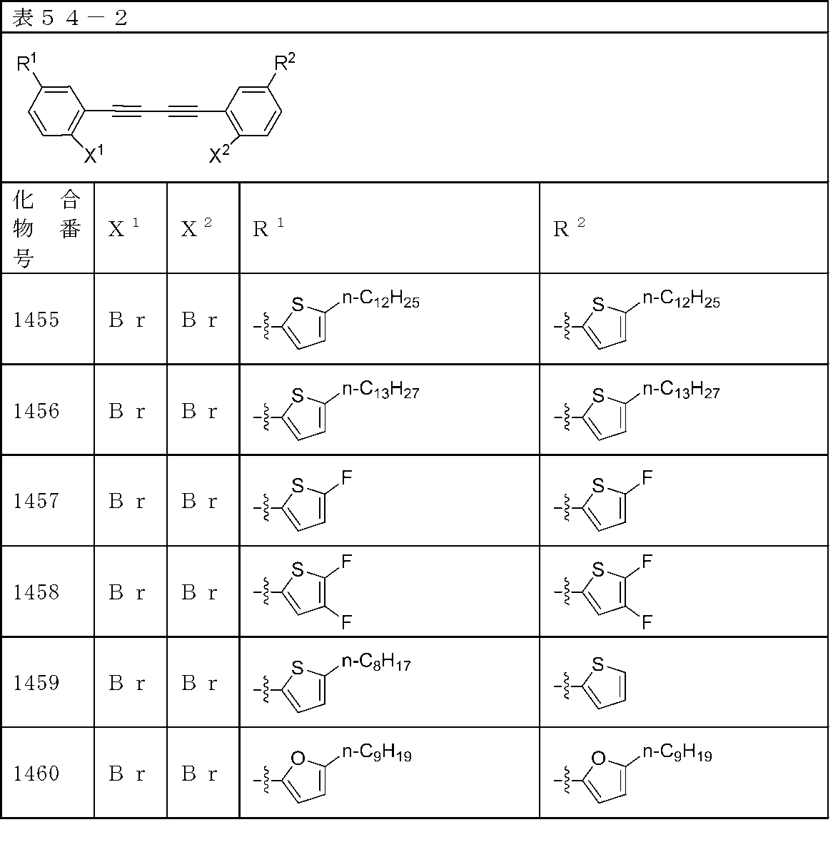

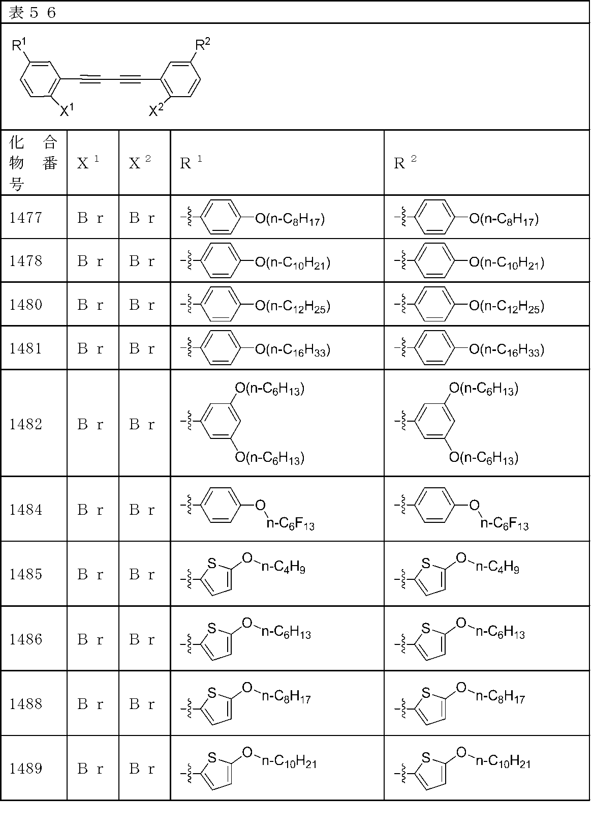


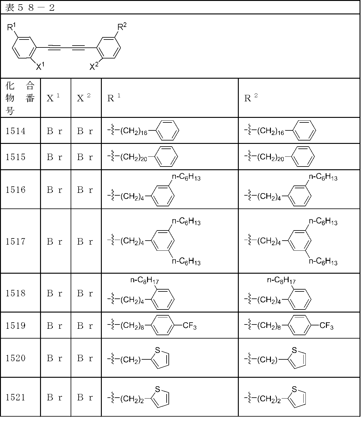
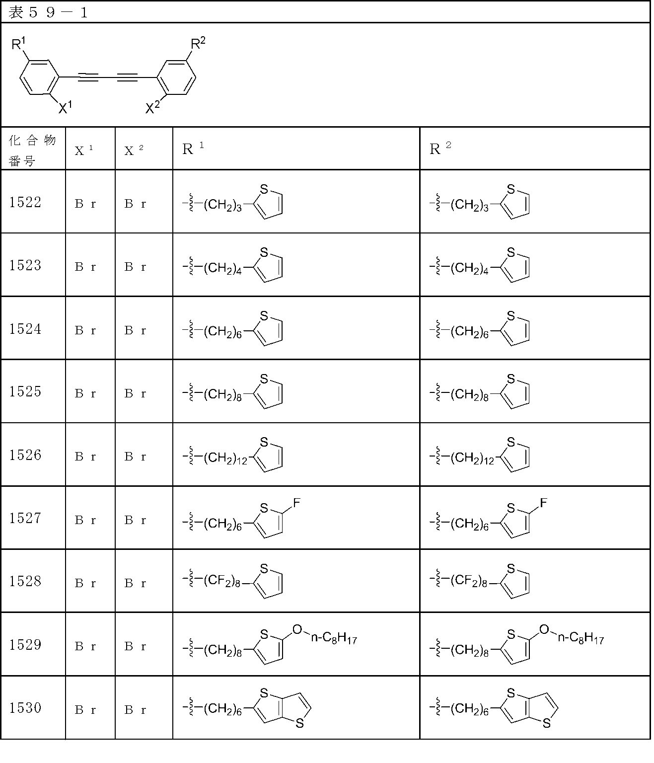


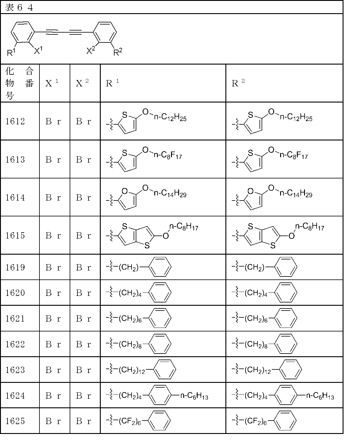
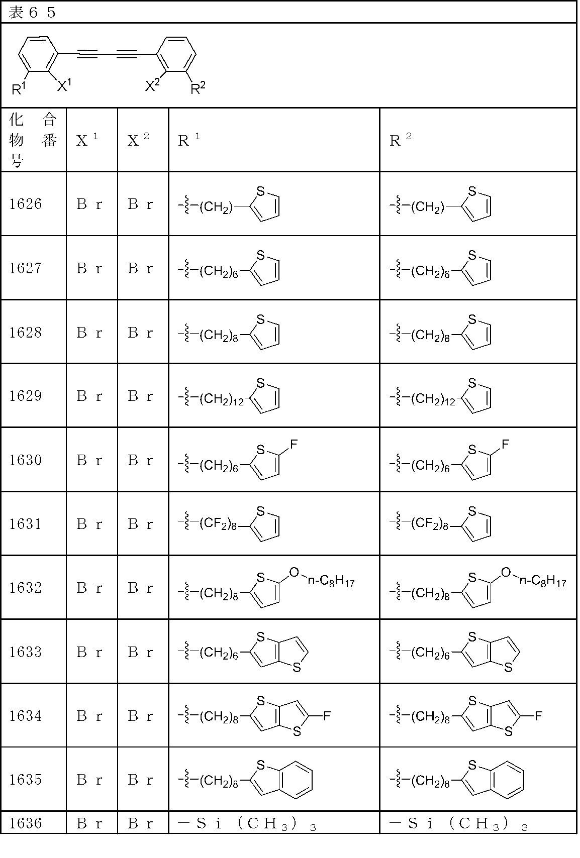

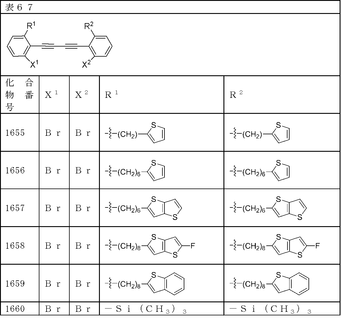

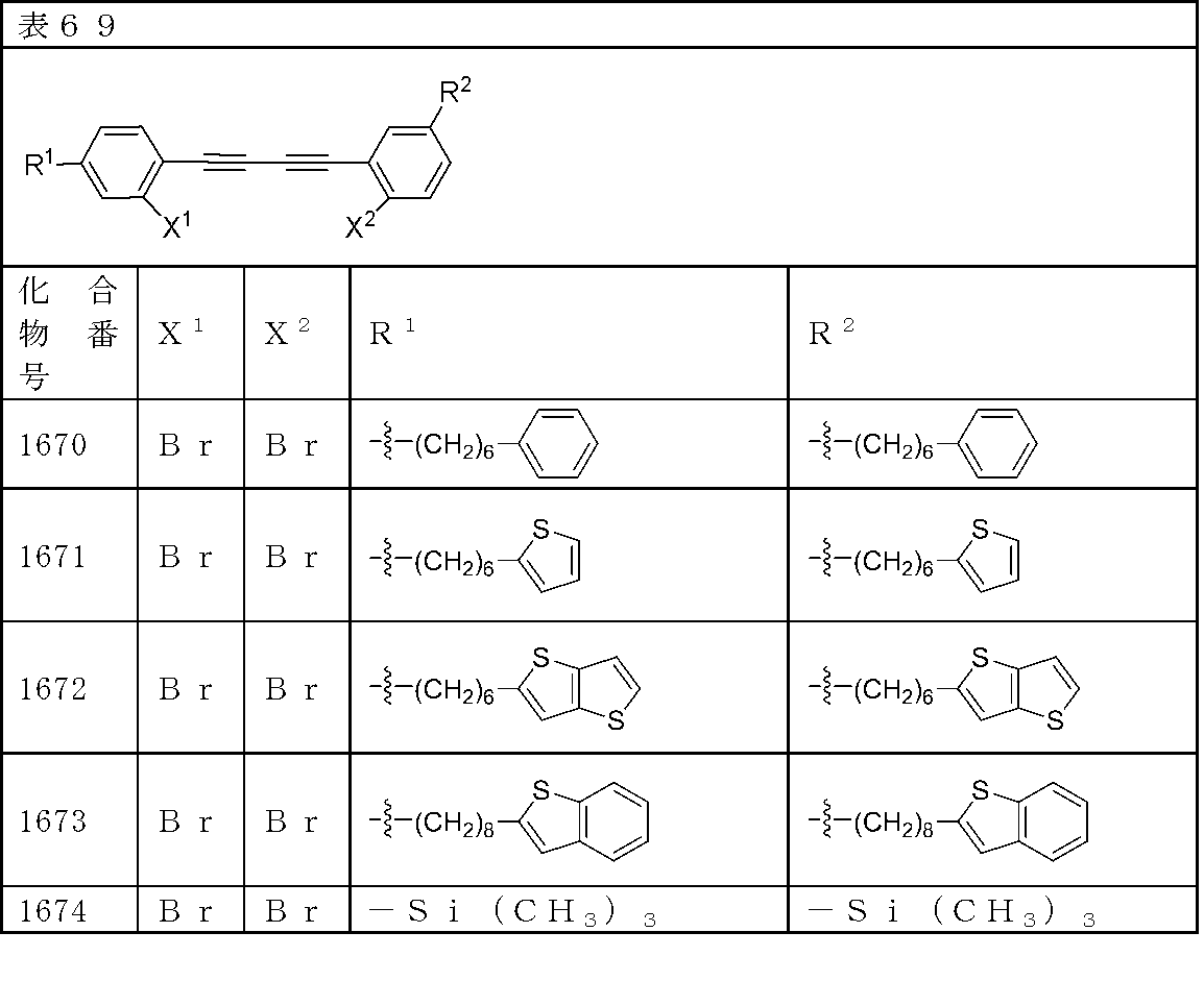















で表される化合物を用いて、いわゆる、グラーゼル反応(Glaser Reaction)、エグリントンカップリング(Eglinton Coupling)又はヘイカップリング(Hay Coupling)(好ましくは、ヨウ化銅などの銅化合物を用いるヘイカップリング)によって調製することができる。
ヘイカップリングは、例えば、下記に示すように、N,N,N’,N’-テトラメチルエチレンジアミン(TMEDA)及びヨウ化銅などの銅化合物の存在下で行うことができる。




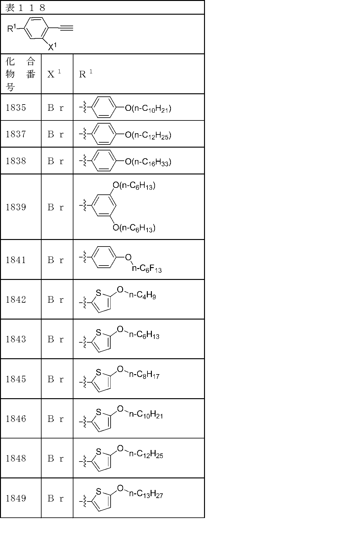
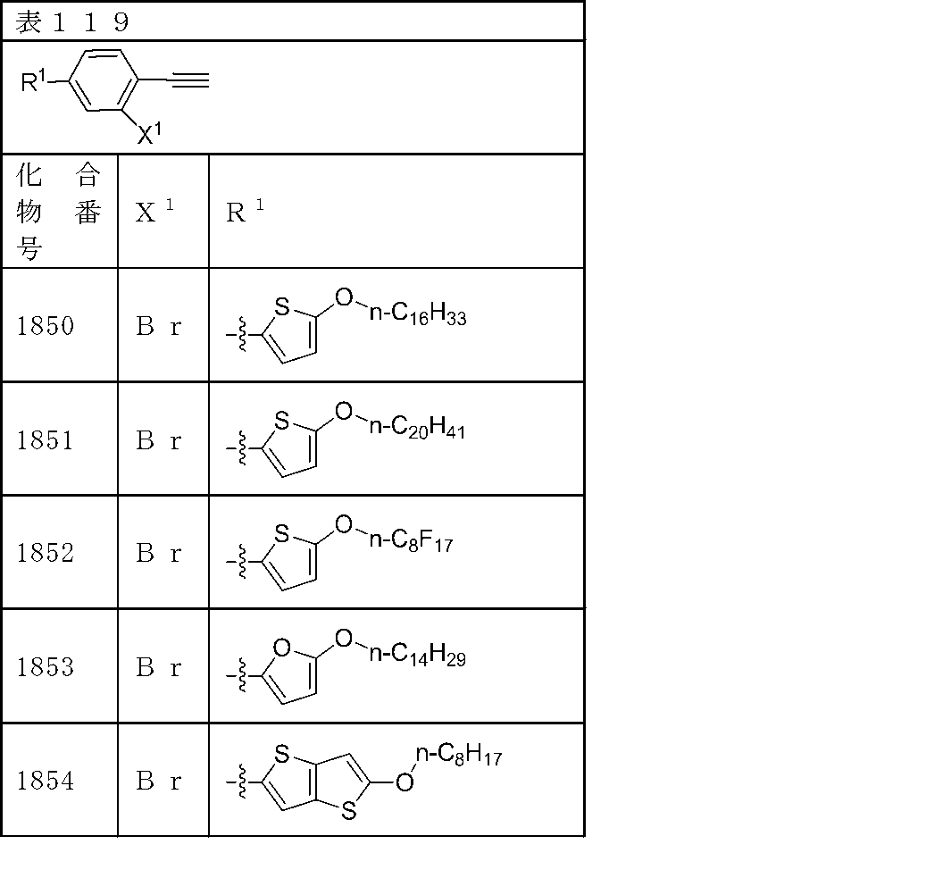
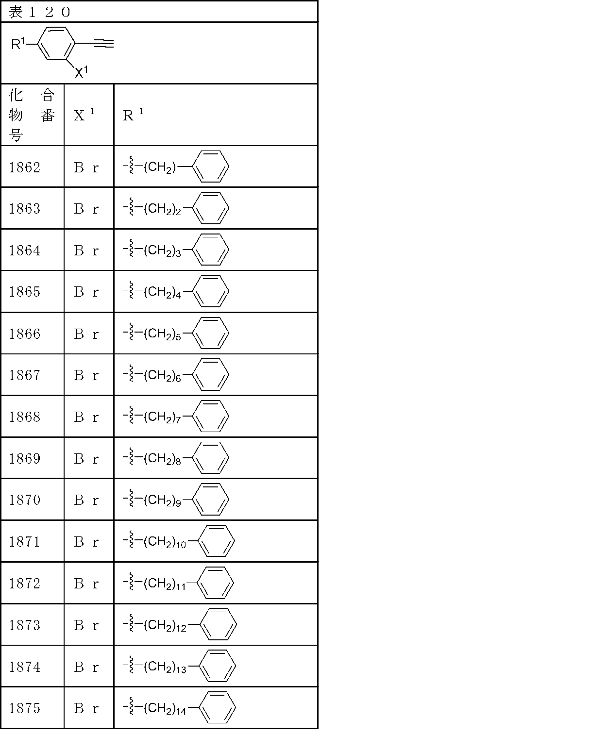
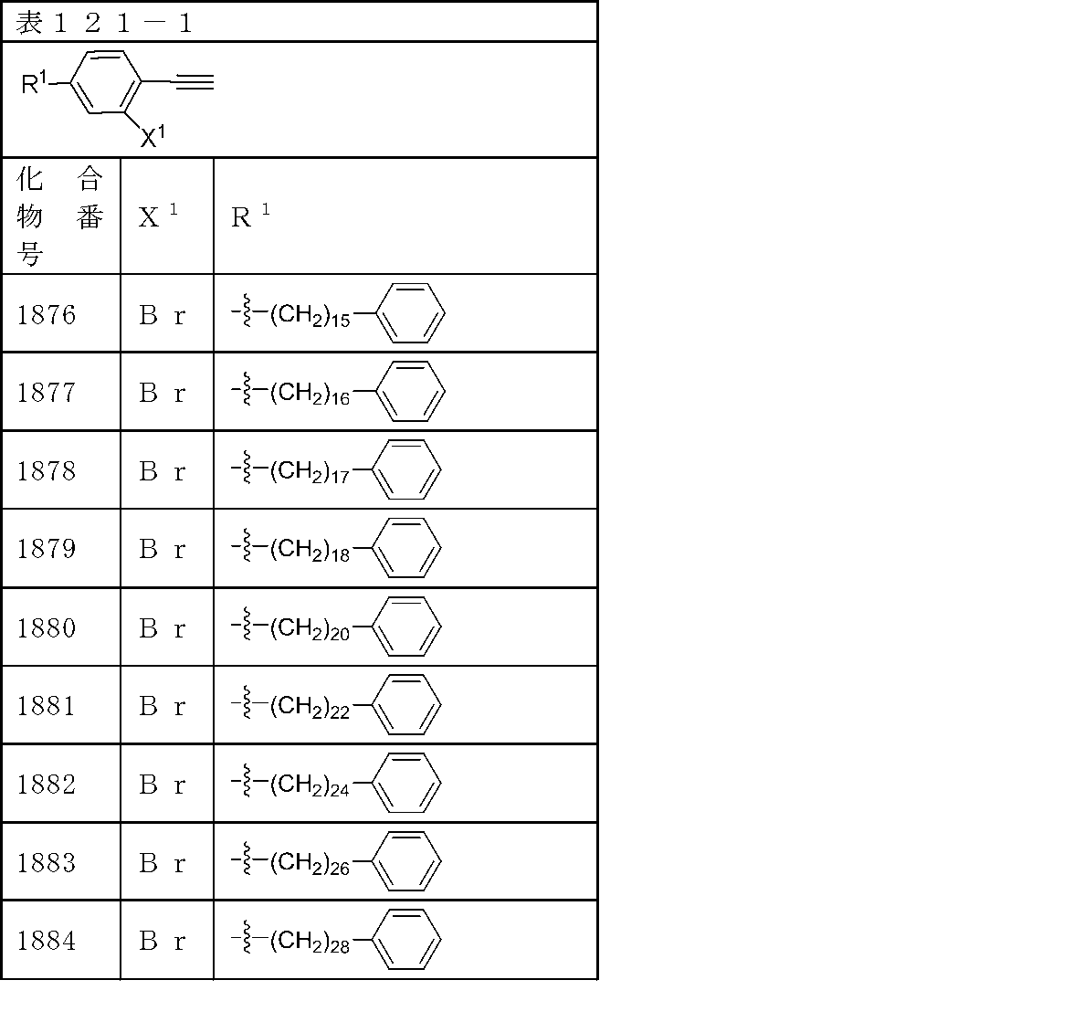

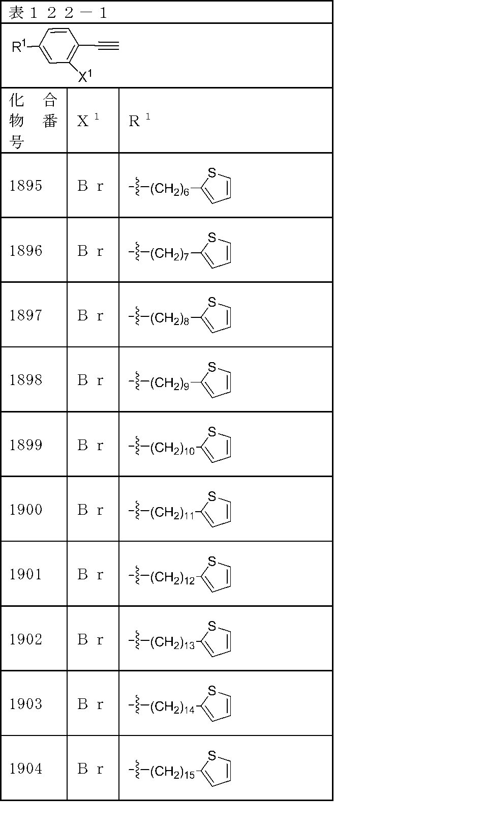

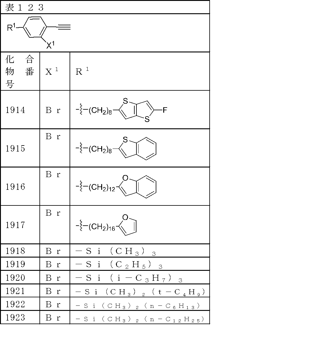
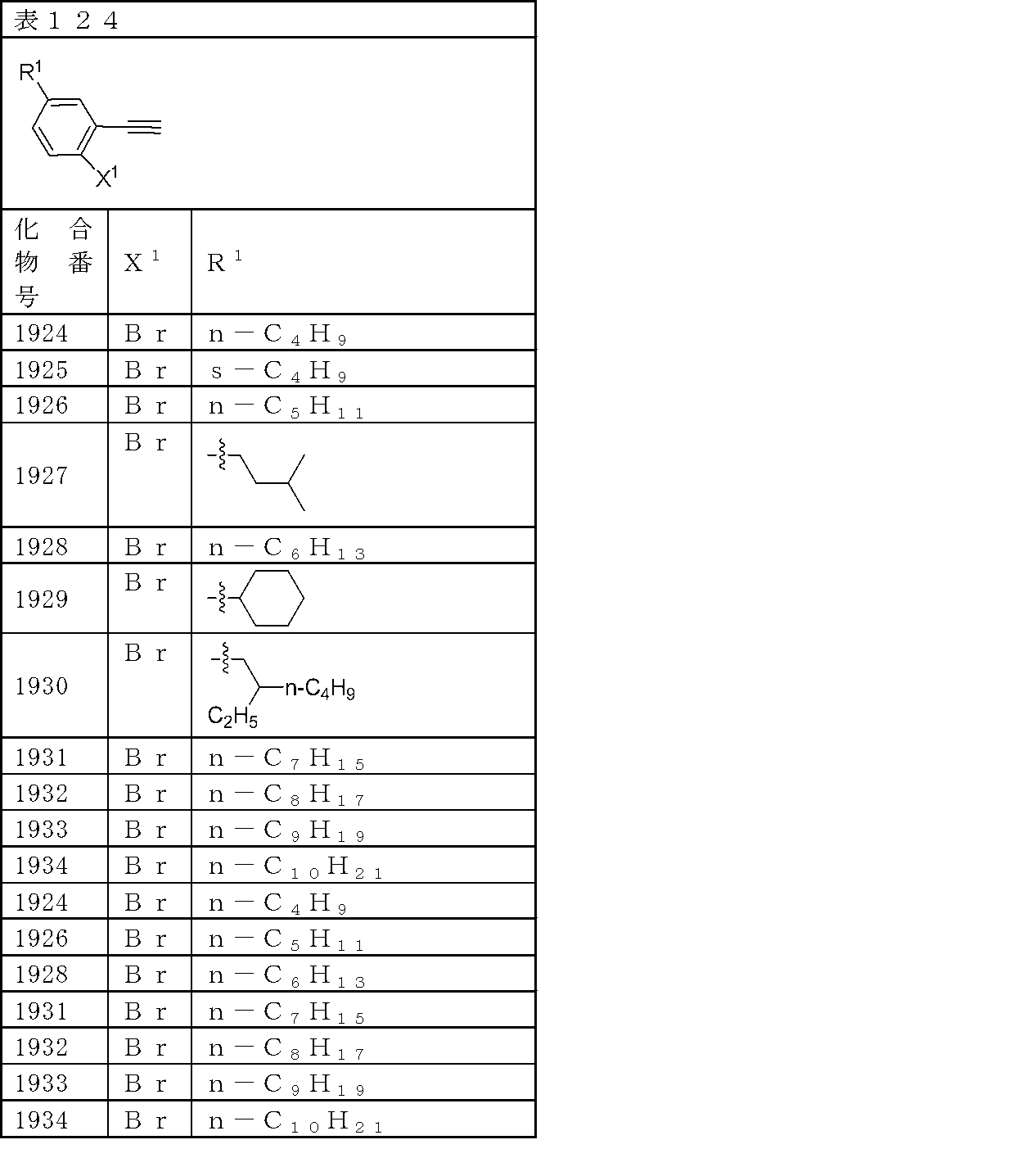
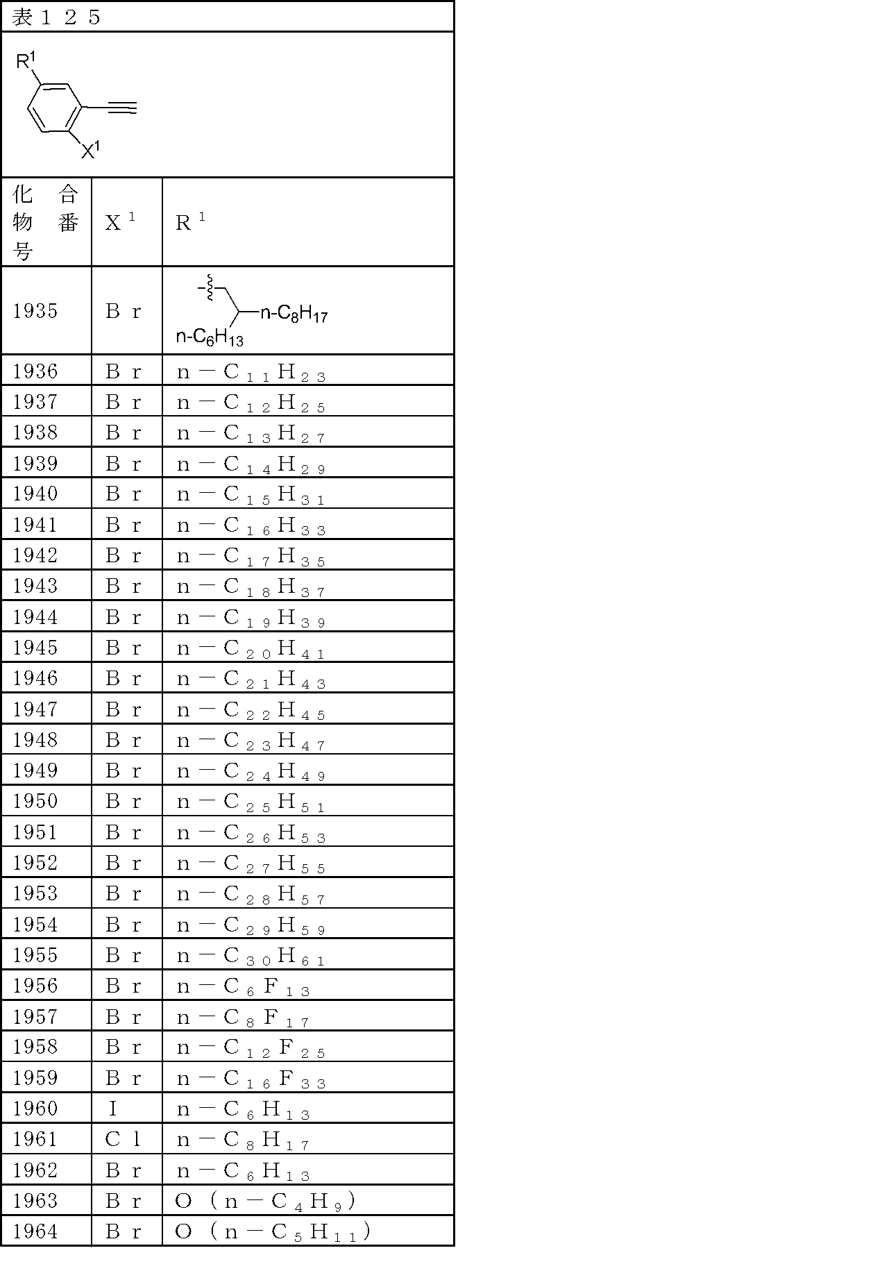
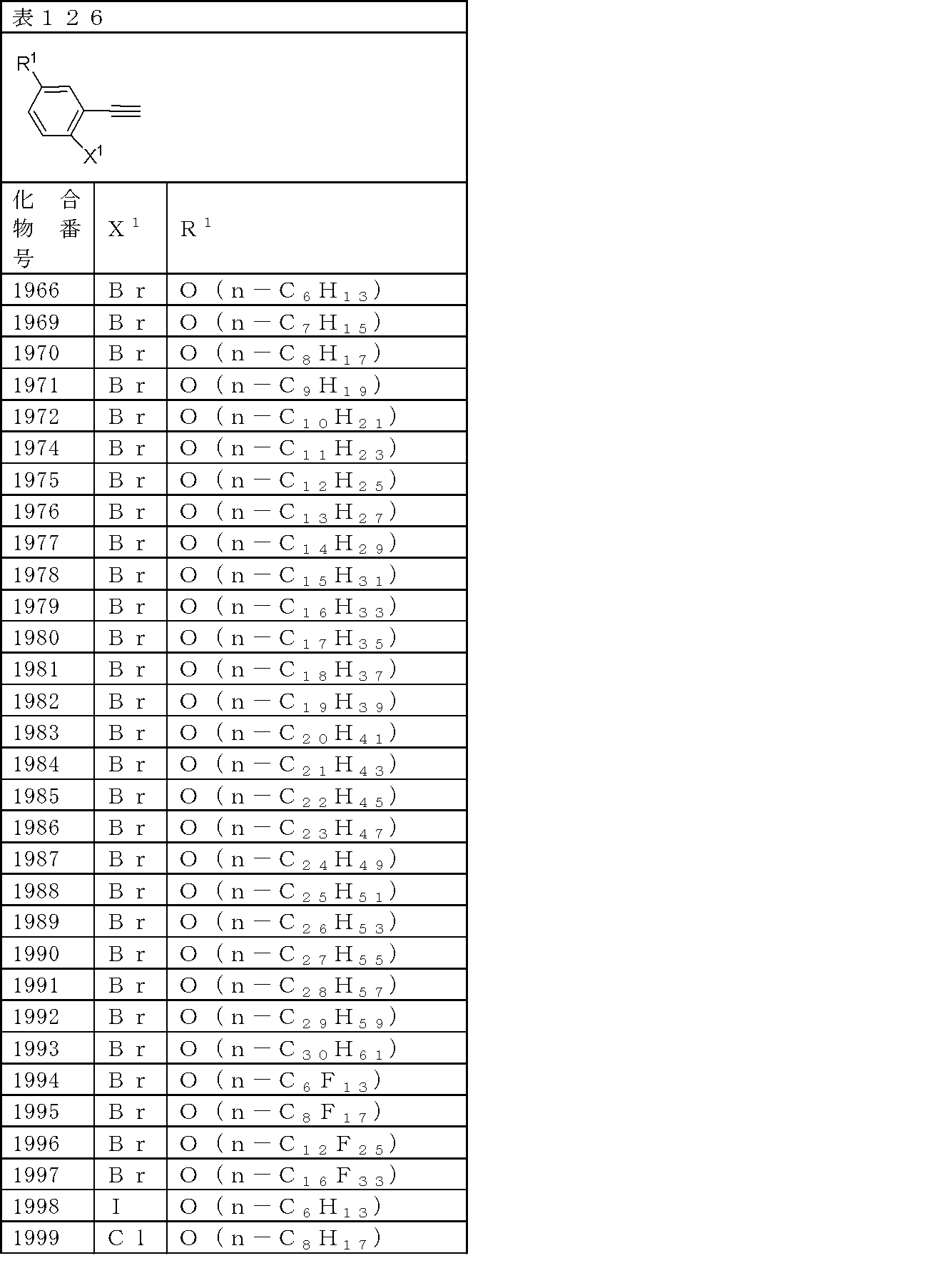


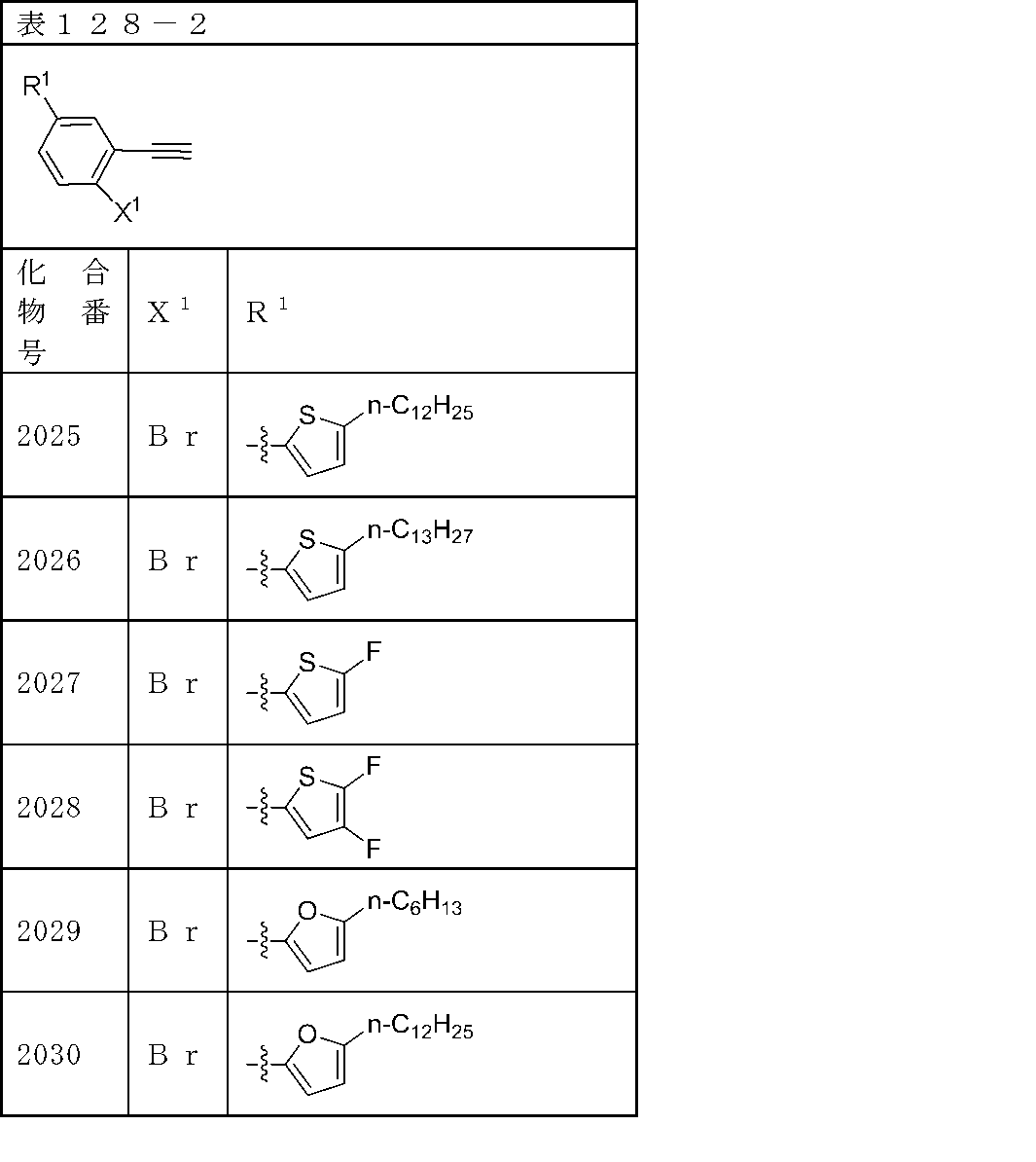
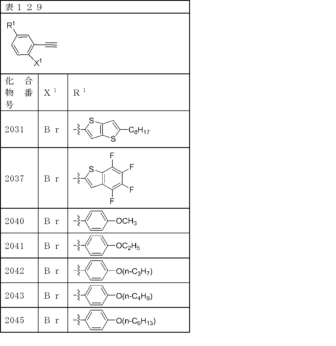


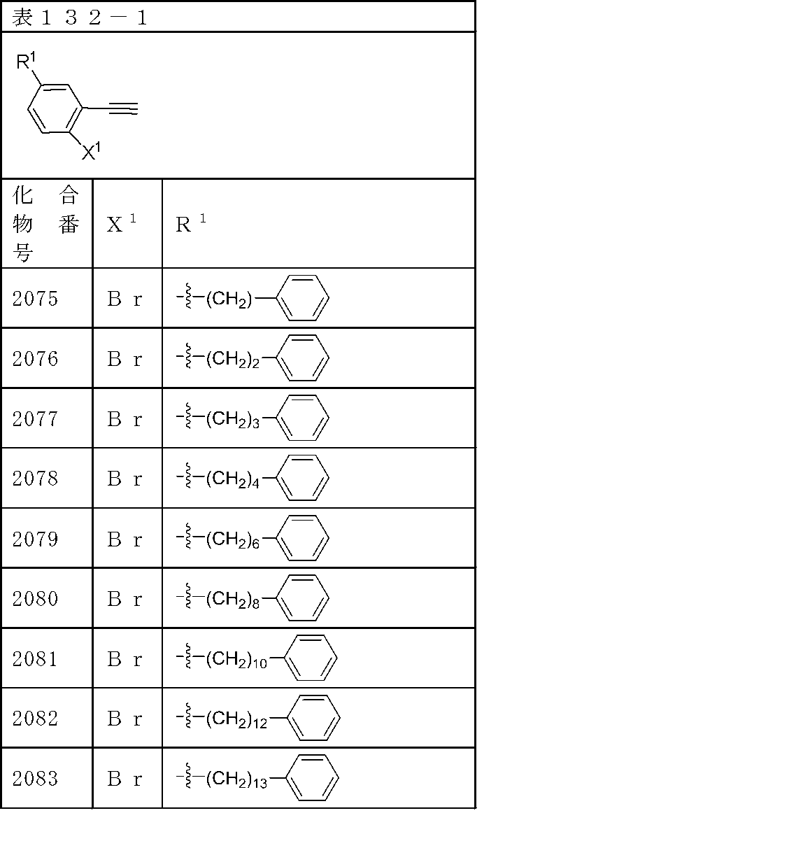

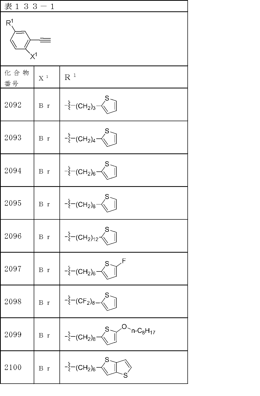


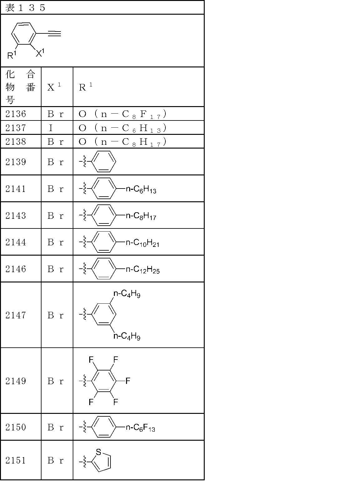
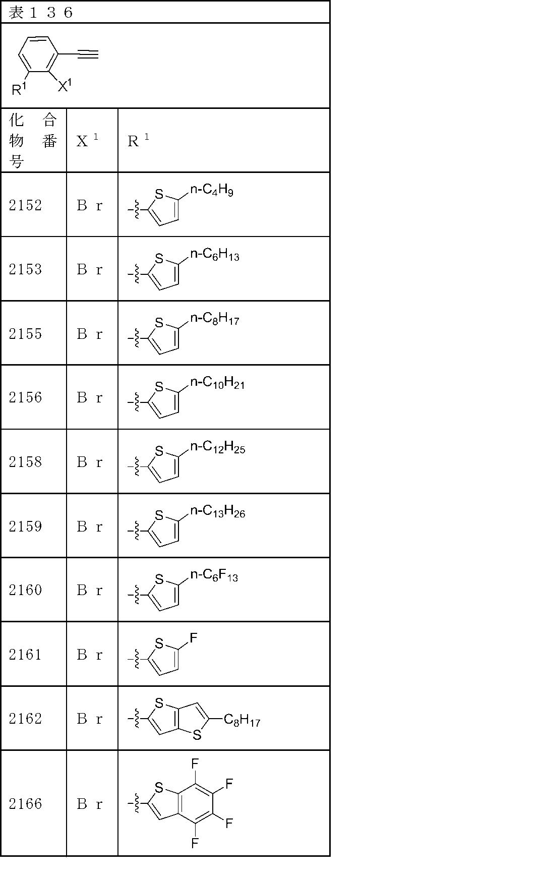


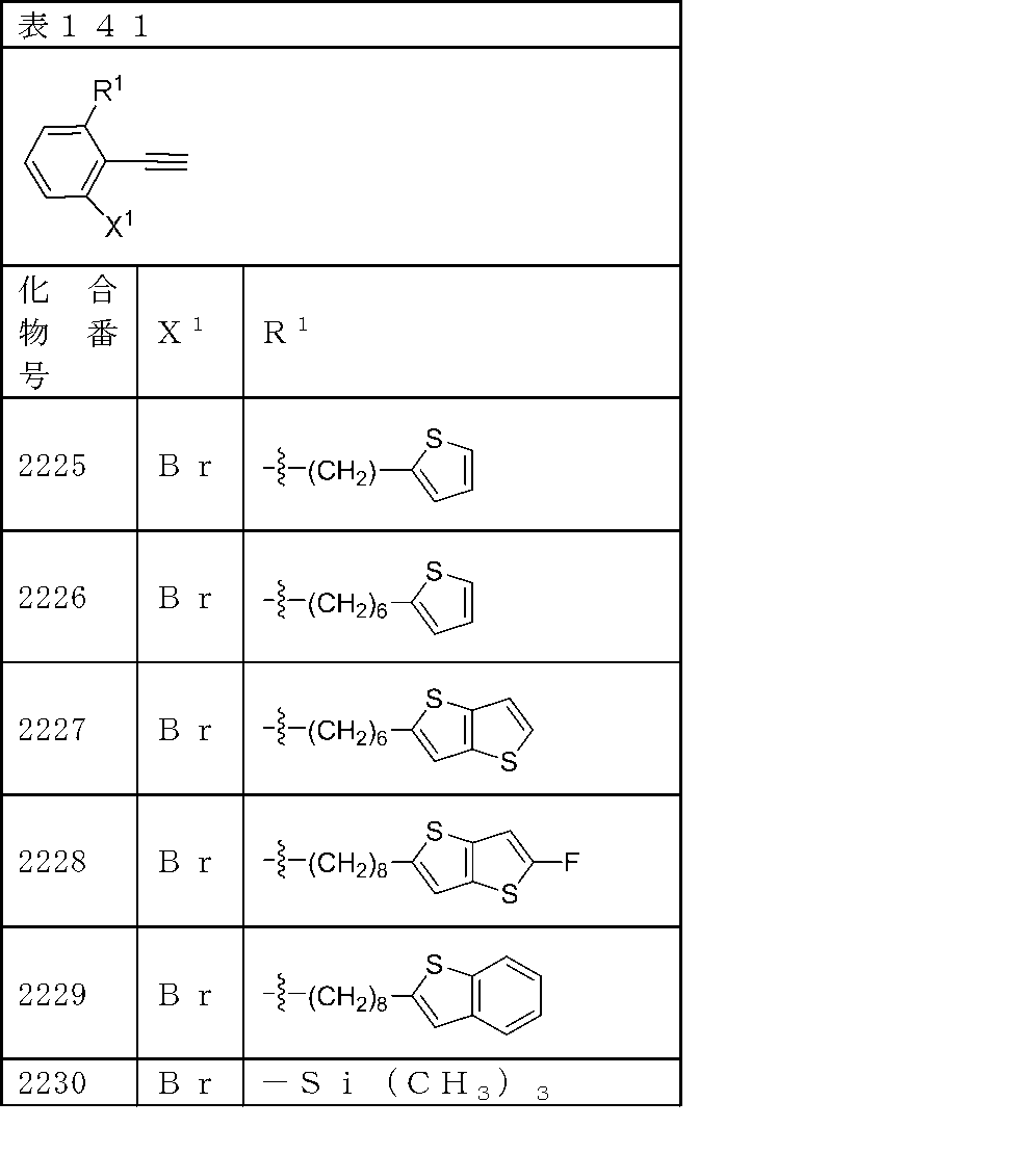

本発明の薄膜は、置換ベンゾカルコゲノアセン化合物(1)を含有する。該薄膜は高いキャリア移動度を示すことから、該薄膜を有機半導体活性層として有する有機半導体デバイスの材料として好適である。
また、本発明の有機半導体デバイスは、本発明の薄膜を含有するものである。本発明の有機半導体デバイスとしては、例えば、有機トラジスタ、電界発光素子、太陽電池等を挙げることができる。また、本発明の有機トランジスタは、例えば、電子ペーパー、フレキシブルディスプレイ、ICタグ、及びセンサ等に使用可能である。
塗布の方法としては、キャスティング法、ディップコート法、ダイコーター法、ロールコーター法、バーコーター法、スピンコート法、インクジェット法、スクリーン印刷法、オフセット印刷法、マイクロコンタクト印刷法などが挙げられる。これらの手法は、単独で用いてもよいし、2種以上を組み合わせてもよい。
このように、本発明の薄膜は、上記の塗布成膜加工等の簡便な方法により形成することができる。
該有機電界効果トランジスタの構造は、通常、ソース電極及びドレイン電極が本発明の薄膜からなる有機半導体活性層に接して設けられており、さらに有機半導体活性層に接した絶縁層(誘電体層)を挟んでゲート電極が設けられていればよい。その素子構造としては、例えば、
(1)基板/ゲート電極/絶縁体層/ソース電極・ドレイン電極/有機半導体活性層 という構造(図1参照)、
(2)基板/ゲート電極/絶縁体層/有機半導体活性層/ソース電極・ドレイン電極 という構造(図2参照)
(3)基板/有機半導体活性層/ソース電極・ドレイン電極/絶縁体層/ゲート電極 という構造
(4)基板/ソース電極(又はドレイン電極)/有機半導体活性層+絶縁体層+ゲート電極/ドレイン電極(又はソース電極)という構造などがあげられる。このとき、ソース電極,ドレイン電極, ゲート電極は、それぞれ複数設けてもよい。また、複数の有機半導体活性層を同一平面内に設けてもよいし、積層して設けてもよい。
本発明における、有機トランジスタの作製において、ソース電極、ドレイン電極及びゲート電極を形成する材料は導電性材料であれば特に限定されず、白金、金、銀、ニッケル、クロム、銅、鉄、錫、アンチモン鉛、タンタル、インジウム、パラジウム、テルル、レニウム、イリジウム、アルミニウム、ルテニウム、ゲルマニウム、モリブデン、酸化モリブデン、タングステン、酸化スズ・アンチモン、酸化インジウム・スズ(ITO)、フッ素ドープ酸化亜鉛、亜鉛、炭素、グラファイト、グラッシーカーボン、銀ペースト及びカーボンペースト、リチウム、ベリリウム、ナトリウム、マグネシウム、カリウム、カルシウム、スカンジウム、チタン、マンガン、ジルコニウム、ガリウム、ニオブ、ナトリウム、ナトリウム-カリウム合金、マグネシウム、リチウム、アルミニウム、マグネシウム/銅混合物、マグネシウム/銀混合物、マグネシウム/アルミニウム混合物、マグネシウム/インジウム混合物、アルミニウム/酸化アルミニウム混合物、リチウム/アルミニウム混合物等が用いられるが、特に、白金、金、銀、酸化モリブデン、インジウム、ITO、炭素が好ましい。又は、ドーピング等で導電率を向上させた公知の導電性ポリマー、例えば、導電性ポリアニリン、導電性ポリピロール、導電性ポリチオフェン、ポリエチレンジオキシチオフェンとポリスチレンスルホン酸の錯体等も好適に用いられる。中でも半導体層との接触面において電気抵抗が少ないものが好ましい。これらの導電性材料は単独で使用してもよいし、2種類以上を混合して使用してもよい。電極の膜厚は、材料によっても異なるが、好ましくは0.1nm~10μmであり、さらに好ましくは0.5nm~5μmであり、より好ましくは1nm~3μmである。また、ゲート電極と基板を兼ねる場合は上記の膜厚より大きくてもよい。
無機酸化物としては、酸化ケイ素、酸化アルミニウム、酸化タンタル、酸化チタン、酸化スズ、酸化バナジウム、チタン酸バリウムストロンチウム、ジルコニウム酸チタン酸バリウム、ジルコニウム酸チタン酸鉛、チタン酸鉛ランタン、チタン酸ストロンチウム、チタン酸バリウム、フッ化バリウムマグネシウム、チタン酸ビスマス、チタン酸ストロンチウムビスマス、タンタル酸ストロンチウムビスマス、タンタル酸ニオブ酸ビスマス、トリオキサイドイットリウムなどが挙げられ、好ましくは、酸化ケイ素、酸化アルミニウム、酸化タンタル、酸化チタンである。無機窒化物としては、窒化ケイ素、窒化アルミニウム等が挙げられる。有機化合物としては、ポリイミド、ポリアミド、ポリエステル、ポリアクリレート、光ラジカル重合又は光カチオン重合して得られる光硬化性樹脂、アクリロニトリル成分を含有する共重合体、ポリビニルフェノール、ポリビニルアルコール、ノボラック樹脂、シアノエチルプルランなどが挙げられ、好ましくは、ポリイミド、ポリビニルフェノール、ポリビニルアルコールが挙げられる。これらの絶縁体層の材料は単独で使用してもよいし、2種類以上を組み合わせて使用してもよい。
絶縁体層の膜厚は、材料によっても異なるが、好ましくは0.1nm~100μmであり、さらに好ましくは0.5nm~50μmであり、より好ましくは5nm~10μmである。
保護膜の形成により、外気の影響を抑制してトランジスタの駆動を安定化することができる。
<製造例1:2-ブロモ-4-ヘキシルアニリンの合成>

シリカゲルカラムによって精製することにより、2-ブロモ-4-ヘキシルアニリンを得た。(35.63g、139.1mmol、収率48.8%)。
1H-NMR(CDCl3、δppm):7.22(d,J=1.9Hz,1H)、6.91(dd,J=8.1、1.9Hz,1H)、6.68(d,J=8.1Hz,1H)、3.93(s、2H)、2.46(t,J=7.7Hz,2H)、1.62-1.47(m、2H)、1.36-1.24(m,6H)、0.88(t,J=6.8Hz,3H)

1H-NMR(CDCl3、δppm):7.72(d,J=8.1Hz,1H)、7.45(d,J=2.0Hz,1H)、6.81(dd,J=8.1,2.0Hz,1H)、2.52(t,J=7.5Hz,2H)、1.59-1.54(m、2H)、1.36-1.29(m,6H)、0.88(t,J=6.7Hz,3H)
MS-EI 366,368(M+)、299,297(M-C5H11)、217(M-C5H11Br)

1H-NMR(CDCl3、δppm):7.42(d,J=7.8Hz,1H)、7.41(d,J=1.8Hz,1H)、7.07(dd,J=7.8,1.8Hz,1H)、3.32(s,1H)、2.57(t,J=7.7Hz,2H)、1.67-1.51(m、2H)、1.37-1.22(m,6H)、0.88(t,J=6.7Hz,3H)
MS-EI 266,264(M+)、195,193(M-C5H11)、115(M-C5H11Br)

1H-NMR(CDCl3、δppm):7.46(d,J=7.8Hz,2H)、7.42(d,J=1.6Hz,2H)、7.08(dd,J=7.8,1.6Hz,2H)、2.58(t,J=7.6Hz,4H)、1.66-1.50(m、4H)、1.38-1.23(m,12H)、0.88(t,J=6.7Hz,6H)
MS-EI 528(M+)、457(M-C5H11)、386(M-C10H22)

1H-NMR(CDCl3、δppm):7.69(d,J=8.1Hz,2H)、7.63(d,J=1.6Hz,2H)、7.28(dd,J=8.1,1.6Hz,2H)、2.74(t,J=7.6Hz,4H)、1.72-1.62(m、4H)、1.40-1.24(m,12H)、0.89(t,J=6.8Hz,6H)

1H-NMR(CDCl3、δppm):7.65(d,J=7.3Hz,2H)、7.57(d,J=1.0Hz,2H)、7.19(dd,J=7.3,1.0Hz,2H)、2.73(t,J=7.0Hz,4H)、1.73-1.63(m、4H)、1.40-1.29(m,12H)、0.90(t,J=6.8Hz,6H)
元素分析:C28H32S3に対する計算値:C72.36、H6.94;測定値:C72.34、H6.85
融点:236℃

上記で得られたオイルのうち96.97gを原料として、水(2.14L)、濃硫酸(142.5L)、亜硫酸ナトリウム(NaSO3:25.57g)、ヨウ化カリウム(KI:378.5g)を用い、2-ブロモ-4-ヘキシル-1-ヨードベンゼンの製造例2と同様な操作を行うことにより、2-ブロモ-4-ドデシル-1-ヨードベンゼンを主成分とする褐色オイル104.72gを得た。
上記で得られたオイルのうち104.0gを原料として、テトラキス(トリフェニルホスフィン)パラジウム(Pd(PPh3)41.01g)、ヨウ化銅(CuI:0.548g)、ジイソプロピルアミン((i-Pr)2NH:88mL)、トリメチルシリルアセチレン(Me3Si-C≡CH(TMS-C≡CH):15.5g)を用い、2-ブロモ-4-ヘキシル-1-(トリメチルシリル)エチニルベンゼンの製造例3と同様な操作を行うことにより、2-ブロモ-4-ドデシル-1-(トリメチルシリル)エチニルベンゼンを主成分とする淡褐色オイル76.34gを得た。上記で得られたオイルのうち73.88gを原料として、テトラヒドロフラン(220mL)、メタノール(220mL)、炭酸カリウム(1.52g)を用い、2-ブロモ-1-エチニル-4-ドデシルベンゼンの製造例3と同様な操作を行うことにより、式[1724]で示される化合物を主成分とする淡褐色オイル65.01gを得た。
得られたオイルのうち64.0gをヨウ化銅(CuI:1.10g)、N,N,N’,N’-テトラメチルエチレンジアミン(TMEDA:1.72mL)のアセトン溶液(120mL)に加えて、室温下、11時間攪拌した。アセトンを減圧留去し、残渣に1N塩酸を加え、つづいてクロロホルムにて抽出した。水および食塩水で洗浄後、硫酸マグネシウムで乾燥し、濃縮した。得られたタール状の残渣をヘキサンに溶かし、その溶液を濃縮することで黄白色粉末である、式[1154]で示される化合物(以下、化合物[1154]と記すことがある。)を得た(22.27g、32.97mmol、収率12%)。
1H-NMR(CDCl3、δppm):7.46(d,J=7.8Hz,2H)、7.42(d,J=1.6Hz,2H)、7.09(dd,J=7.8,1.4Hz,2H)、2.58(t,J=8.1Hz,4H)、1.64-1.52(m、4H)、1.35-1.21(m,36H)、0.88(t,J=7.0Hz,6H)

1H-NMR(CDCl3、δppm):7.69(d,J=8.4Hz,2H)、7.62(d,J=0.8Hz,2H)、7.28(dd,J=8.1,1.4Hz,2H)、2.74(t,J=7.8Hz,4H)、1.73-1.61(m、4H)、1.38-1.22(m,36H)、0.88(t,J=7.0Hz,6H)

1H-NMR(CDCl3、CS2 δppm):7.75(d,J=8.1Hz,2H)、7.67(d,J=0.8Hz,2H)、7.26(dd,J=8.1,1.6Hz,2H)、2.75(t,J=7.6Hz,4H)、1.73-1.65(m、4H)、1.40-1.22(m,36H)、0.88(t,J=7.3Hz,6H).
HRMS(EI):C40H56S3に対する計算値:632.3531(M+);測定値:632.3544
元素分析値:C40H56S3に対する計算値:C75.89、H8.92;測定値 C75.92、H8.94
融点:194℃
SiO2熱酸化膜付きnドープシリコンウエハー上に、ヘキサメチルジシラザンをスピンコートにより成膜した基板に、金属マスクを用いてクロムを3nm、金を50nm順次真空蒸着して電極を作成した。作成した電極のチャネル幅及びチャネル長は、それぞれ、2000μm及び20μmであった。次に実施例1で合成した化合物[5]を昇華により精製した試料を石英製のるつぼに入れ、るつぼを加熱し、真空蒸着法により、化合物[5]からなる薄膜を形成した。
真空蒸着法に用いた装置チェンバ内の真空度は、1×10⁻⁴パスカル以下であり、基板の温度は、室温(24℃)以上80℃以下の範囲であった。薄膜の膜厚は、約200nmであった。
このようにして、昇華により精製した化合物[5]からなる薄膜をもつ有機トランジスタ(図1参照)を製造することができた。
実施例3で作製した化合物[5]からなる薄膜をもつ有機トランジスタの電気特性はパラメーターアナライザーを用いて真空下で測定した。その結果、ゲート電極(Vg)に負のゲート電圧の印加を増加させると、負のドレイン電流(Id)が増加することから、製造した化合物[5]からなる薄膜をもつ有機トランジスタは、p型の有機トランジスタであることを確認することができた。負のゲート電圧(Vg)において、ドレイン電圧(Vd)に対するドレイン電流(Id)の変化曲線は、良好であり、高いドレイン電圧において飽和領域を有していた。さらに、有機トランジスタのキャリアの飽和電界効果移動度μは、有機トランジスタの電気的特性の飽和領域におけるドレイン電流Idを表す式
Id=(W/2L)μCi(Vg-Vt)2 ・・・(a)
を用いて算出することができる。ここで、L及びWは、それぞれ、有機トランジスタのチャネル長及びチャネル幅であり、Ciは、ゲート電極用の絶縁体層(以下、ゲート絶縁膜と記すことがある)の単位面積当たりの静電容量であり、Vgは、ゲート電圧であり、Vtは、ゲート電圧のしきい値電圧である。式(a)を用いて、製造した化合物[5]からなる薄膜をもつ有機トランジスタのキャリアの飽和電界効果移動度μを計算した結果、基板の温度60℃で製造した化合物[5]からなる薄膜をもつ有機トランジスタにおけるキャリアの飽和電界効果移動度(キャリア移動度)は1.6cm2/Vsであった。また、ドレイン電圧Vdが-50Vにおける、ゲート電圧が0Vと-50V時のドレイン電流Id値の比(以下、オン/オフ比と記すことがある)は、107であった。
実施例1で製造した化合物[5]をテトラヒドロフランに溶解して、化合物[5]の濃度が0.5重量%の溶液組成物を調製した。
この溶液組成物を、ヘキサメチルジシラザン処理を行ったSiO2熱酸化膜付きnドープシリコンウエハー上にスピンコート法により塗布し、化合物[5]からなる薄膜を形成した。さらに形成した薄膜を80℃にて30分保温した。薄膜の膜厚は、約30nmであった。
実施例5で得られた薄膜に、金属マスクを用いて酸化モリブデン、続いて金の層を真空蒸着法で、上記薄膜上に成膜して、ソース電極及びドレイン電極を形成した。ここで、ソース電極及びドレイン電極を形成することによって得られた有機TFTのチャネル幅及びチャネル長は、それぞれ、2000μm及び20μmであった。このようにして、図2に示すような、化合物[5]を含有する薄膜をもつ有機トランジスタを作製することができた。
実施例6で製造した有機トランジスタの電気特性を実施例4と同様に測定した結果、キャリアの電界効果移動度(キャリア移動度)及びオン/オフ比はそれぞれ、0.3cm2/Vs及び107であった。
SiO2熱酸化膜付きnドープシリコンウエハー上に、チャネル幅2000μm、チャネル長20μmのソース電極、ドレイン電極(SiO2熱酸化膜側から、クロム、金の順)を作製した。この基板をアセトンで10分間超音波洗浄した後、オゾンUVを20分間照射した。その後、フェニルエチルトリクロロシランのトルエン希釈液を用い、これに基板を2分間浸漬することによりこの基板表面をシラン処理した。さらに、パーフルオロベンゼンチオールのイソプロピルアルコール希釈液を用い、これに基板を2分間浸漬することにより基板上に形成したAu電極表面を修飾することにより、トランジスタ基板を作製した。
次に実施例2で合成した化合物[14]を石英製のるつぼに入れ、るつぼを加熱し、真空蒸着法により、化合物[14]からなる薄膜をトランジスタ基板上に形成した。真空蒸着法に用いた装置チェンバ内の真空度は、1×10⁻⁴パスカル以下であり、基板の温度は、80℃であった。薄膜の膜厚は、約100nmであった。
実施例8で得られた有機薄膜トランジスタ素子のドレイン電圧(Vd)を-40Vに設定し、ゲート電圧Vgを20~-40Vに変化させた条件で、そのトランジスタ特性を測定した。かかる測定により得られた伝達特性から算出した、有機薄膜トランジスタによる電界効果移動度(移動度)は0.4cm2/Vs、オン/オフ比は107であった。
実施例8と同様にして得られた基板上に化合物[14]の0.5重量%ジクロロベンゼン溶液を100℃に加熱してスピンコート法により塗布し、120℃のホットプレートで30分間乾燥させることにより、約30nmの厚さを有する化合物の薄膜を形成した。
上述のようにして得られた有機薄膜トランジスタ素子のドレイン電圧(Vd)を-40Vに設定し、ゲート電圧(Vg)を20~-40Vに変化させた条件で、そのトランジスタ特性を測定した。かかる測定により得られた伝達特性から算出した、有機薄膜トランジスタによる電界効果移動度は0.5cm2/Vs、オン/オフ比は107であった。

4-ドデシルアニリンの代わりに4-ペンチルオキシアニリンを用いる以外は、製造例7、製造例8及び実施例2と同様にして、化合物[41](表2の化合物番号41の化合物を意味する。)を得ることができる。
得られる化合物[41]を用いて、実施例8と同様にしてトランジスタ基板の作成を行い、続いて、実施例10と同様にして該薄膜をもつ有機トランジスタの作製を行う。得られる有機トランジスタの測定を実施例9に準じて行うことにより、高いキャリア移動度の値を得ることができる。
4-ドデシルアニリンの代わりに4-(4-フェニルブチル)アニリンを用いる以外は、製造例7、製造例8及び実施例2と同様にして化合物[155](表9の化合物番号155の化合物を意味する。)を得ることができる。
得られる化合物[155]を用いて、実施例8と同様にしてトランジスタ基板の作成を行い、続いて、実施例10と同様にして該薄膜をもつ有機トランジスタの作製を行う。得られる有機トランジスタの測定を実施例9に準じて行うことにより、高いキャリア移動度の値を得ることができる。
製造例1における4-ヘキシルアニリンに代わり、3-オクチルアニリンを用いる以外は、製造例7、製造例8及び実施例2と同様にして、化合物[218](表13の化合物番号222の化合物を意味する。)を得ることができる。
得られる化合物[222]を用いて、実施例8と同様にしてトランジスタ基板の作成を行い、続いて、実施例10と同様にして該薄膜をもつ有機トランジスタの作製を行う。得られる有機トランジスタの測定を実施例9に準じて行うことにより、高いキャリア移動度の値を得ることができる。
4-ドデシルアニリンの代わりに4-(2-エチルヘキシル)アニリンを用いる以外は、製造例7、製造例8及び実施例2と同様にして化合物[7](表1の化合物番号7の化合物を意味する。)を得ることができる。
4-ドデシルアニリンの代わりに4-(2-ヘキシルデシル)アニリンを用いる以外は、製造例7、製造例8及び実施例2と同様にして化合物[12](表1の化合物番号15の化合物を意味する。)を得ることができる。
4-ドデシルアニリンの代わりに4-トリデシルアニリンを用いる以外は、製造例7、製造例8及び実施例2と同様にして化合物[15](表1の化合物番号15の化合物を意味する。)を得ることができる。
4-ドデシルアニリンの代わりに4-ヘキサデシルアニリンを用いる以外は、製造例7、製造例8及び実施例2と同様にして化合物[18](表2の化合物番号18の化合物を意味する。)を得ることができる。
4-ドデシルアニリンの代わりに4-(2-ヘキシルオクチル)アニリンを用いる以外は、製造例7、製造例8及び実施例2と同様にして化合物[42](表2の化合物番号42の化合物を意味する。)を得ることができる。
4-ドデシルアニリンの代わりに4-(4’-ヘキシルフェニル)アニリンを用いる以外は、製造例7、製造例8及び実施例2と同様にして、化合物[84](表4の化合物番号84の化合物を意味する。)を得ることができる。
4-ドデシルアニリンの代わりに4-[2-(5-ヘキシル)チエニル]アニリンを用いる以外は、製造例7、製造例8及び実施例2と同様にして化合物[97](表5の化合物番号97の化合物を意味する。)を得ることができる。
4-ドデシルアニリンの代わりに4-[(2-ベンゾ[b]チエノ)オクチル]アニリンを用いる以外は、製造例7、製造例8及び実施例2と同様にして化合物[205](表12の化合物番号205の化合物を意味する。)を得ることができる。
Advanced Materials, 19, 3008-3011(2007)に準じて、下記式に従って製造することにより、化合物[208](表12の化合物番号208の化合物を意味する。)を得ることができる。
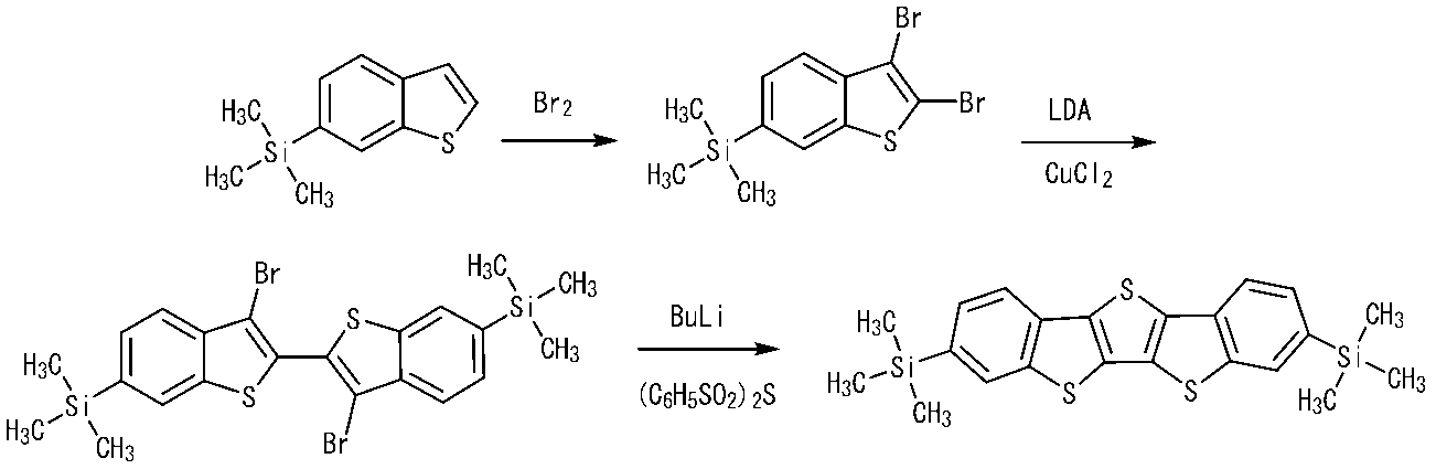
12 ゲート電極
13 ゲート絶縁膜
14 ソース電極
15 ドレイン電極
16 有機半導体活性層
21 基板
22 ゲート電極
23 ゲート絶縁膜
24 ソース電極
25 ドレイン電極
26 有機半導体活性層
Claims (27)
- 式(1)

で表される置換ベンゾカルコゲノアセン化合物。 - 式(1)におけるEが、全て硫黄原子である請求項1記載の化合物。
- 式(1)におけるR1及びR2は、それぞれ独立に、水素原子、フッ素原子を有していてもよい炭素数4~30のアルキル基、フッ素原子を有していてもよい炭素数4~30のアルコキシ基、アルキル基又はアルコキシ基を有していてもよい炭素数6~30のアリール基(該アリール基はフッ素原子を有していてもよい)、フッ素原子を有していてもよい炭素数7~30のアラルキル基、アルキル基又はアルコキシ基を有していてもよい炭素数4~30のヘテロアリール基(該ヘテロアリール基はフッ素原子を有していてもよい)、フッ素原子を有していてもよい炭素数5~30のヘテロアラルキル基である請求項1又は2記載の化合物。
- 式(1)で表される化合物が、式(2)
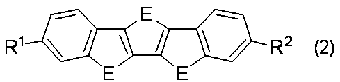
で表される請求項1~3のいずれか記載の化合物。 - 式(2)において、Eはそれぞれ独立に、硫黄またはセレン原子を表す。R1及びR2はそれぞれ独立に、水素原子、フッ素原子を置換基として有していてもよい炭素数4~30のアルキル基又はフッ素原子を置換基として有していてもよい炭素数3~30のトリアルキルシリル基である請求項4記載の化合物。
- 式(2)において、R1及びR2は、それぞれ独立に、炭素数4~30のアルキル基又は炭素数3~30のトリアルキルシリル基である請求項5記載の化合物。
- 式(2)において、R1及びR2が炭素数4~30のアルキル基である請求項5記載の化合物。
- 式(2)において、R1及びR2は、同一であり、かつ、炭素数4~20のアルキル基である請求項5記載の化合物。
- 式(2)において、R1及びR2が炭素数6~12のアルキル基である請求項5記載の化合物。
- 式(2)におけるR1及びR2は、それぞれ独立に、水素原子、フッ素原子を有していてもよい炭素数4~30のアルキル基、フッ素原子を有していてもよい炭素数4~30のアルコキシ基、アルキル基を有していてもよい炭素数6~30のアリール基(該アリール基はフッ素原子を有していてもよい)、フッ素原子を有していてもよい炭素数7~30のアラルキル基である請求項4記載の化合物。
- 式(2)において、R1及びR2は、同一であり、かつ、炭素数4~20のアルコキシ基である請求項4記載の化合物。
- 式(2)において、R1及びR2は、同一であり、かつ、炭素数1~20のアルキル基を有する炭素数6~10のアリール基である請求項4記載の化合物。
- 式(2)において、R1及びR2は、同一であり、かつ、炭素数7~20のアラルキル基である請求項4記載の化合物。
- 式(2)において、R1及びR2はそれぞれ独立に、炭素数3~30のトリアルキルシリル基である請求項5記載の化合物。
- 式(2)において、R1及びR2はそれぞれ独立に、炭素数3~14のトリアルキルシリル基である請求項5記載の化合物。
- 式(2)において、R1及びR2は同一であり、ヘキシル基又はドデシル基である請求項4又は5記載の化合物。
- 式(2)において、Eが、全て硫黄原子である請求項4~16のいずれか記載の化合物。
- 式(2)において、Eが、全て硫黄原子であり、R1及びR2はヘキシル基である請求項4記載の化合物。
- 式(2)において、Eが、全て硫黄原子であり、R1及びR2はドデシル基である請求項4記載の化合物。
- 式(2)において、Eが、全て硫黄原子であり、R1及びR2はそれぞれ独立に、炭素数6~12のアルキル基である請求項4記載の化合物。
- 下記式[5]、[7]、[12]、[14]、[15]、[18]または[42]で示される化合物。
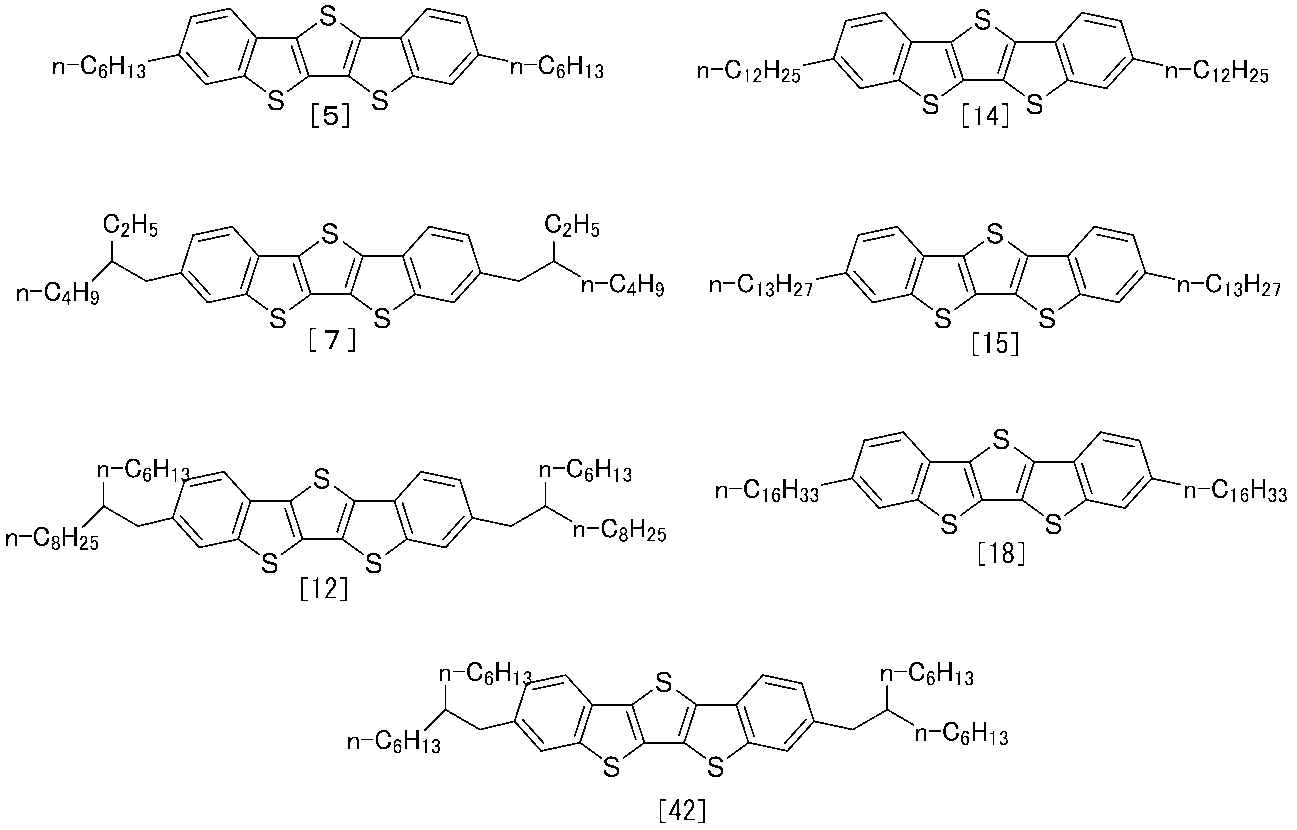
- 式(1)で表される化合物が、式(3)
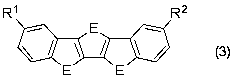
で表される請求項1~3のいずれか記載の化合物。 - 式(3)において、R1及びR2は、同一であり、かつ、炭素数4~20のアルキル基である請求項22記載の化合物。
- 請求項1~23のいずれか記載の化合物を含有する薄膜。
- 請求項1~23のいずれか記載の化合物からなる薄膜。
- 請求項23又は24記載の薄膜を含有する有機半導体デバイス。
- 請求項24又は25記載の薄膜を含有する有機トランジスタ。
Priority Applications (4)
| Application Number | Priority Date | Filing Date | Title |
|---|---|---|---|
| US13/382,821 US20120190868A1 (en) | 2009-07-10 | 2010-07-08 | Substituted benzochalcogenoacene compound, thin film comprising the compound, and organic semiconductor device including the thin film |
| RU2012104635/04A RU2012104635A (ru) | 2009-07-10 | 2010-07-08 | Соединение замещенного бензохалькогенацена, тонкая пленка, включающая такое соединение, и органическое полупроводниковое устройство, включающее такую тонкую пленку |
| CN201080040263.5A CN102574868B (zh) | 2009-07-10 | 2010-07-08 | 取代苯并硫属并苯化合物、包含该化合物的薄膜以及包括该薄膜的有机半导体装置 |
| EP10797180A EP2452942A4 (en) | 2009-07-10 | 2010-07-08 | SUBSTITUTED BENZOCHALCOGENACEN COMPOUND, THIN LAYER WITH THE CONNECTION AND ORGANIC SEMICONDUCTOR COMPONENT WITH THE THIN LAYER |
Applications Claiming Priority (2)
| Application Number | Priority Date | Filing Date | Title |
|---|---|---|---|
| JP2009-163919 | 2009-07-10 | ||
| JP2009163919 | 2009-07-10 |
Publications (1)
| Publication Number | Publication Date |
|---|---|
| WO2011004869A1 true WO2011004869A1 (ja) | 2011-01-13 |
Family
ID=43429294
Family Applications (1)
| Application Number | Title | Priority Date | Filing Date |
|---|---|---|---|
| PCT/JP2010/061634 Ceased WO2011004869A1 (ja) | 2009-07-10 | 2010-07-08 | 置換ベンゾカルコゲノアセン化合物、該化合物を含有する薄膜及び該薄膜を含有する有機半導体デバイス |
Country Status (8)
| Country | Link |
|---|---|
| US (1) | US20120190868A1 (ja) |
| EP (1) | EP2452942A4 (ja) |
| JP (1) | JP2011032268A (ja) |
| KR (1) | KR20120090939A (ja) |
| CN (1) | CN102574868B (ja) |
| RU (1) | RU2012104635A (ja) |
| TW (1) | TW201125871A (ja) |
| WO (1) | WO2011004869A1 (ja) |
Cited By (4)
| Publication number | Priority date | Publication date | Assignee | Title |
|---|---|---|---|---|
| WO2012022935A1 (en) | 2010-08-18 | 2012-02-23 | Cambridge Display Technology Limited | Low contact resistance organic thin film transistors |
| US8372312B1 (en) | 2011-10-17 | 2013-02-12 | Xerox Corporation | Non-symmetrical dibenzodithienothiophene compounds |
| WO2013039842A1 (en) * | 2011-09-12 | 2013-03-21 | Polyera Corporation | Compounds having semiconducting properties and related compositions and devices |
| US9373795B2 (en) | 2011-09-20 | 2016-06-21 | Cambridge Display Technology Limited | Organic semiconductor composition including a non-polymeric material having a polydispersity equal to one, at least one solvent, and a crystallization modifier, and an organic thin-film transistor using the same |
Families Citing this family (11)
| Publication number | Priority date | Publication date | Assignee | Title |
|---|---|---|---|---|
| KR101571590B1 (ko) | 2012-11-21 | 2015-11-25 | 주식회사 두산 | 유기 화합물 및 이를 이용하는 유기 전계 발광 소자 |
| JP2015122383A (ja) * | 2013-12-20 | 2015-07-02 | 三星ディスプレイ株式會社Samsung Display Co.,Ltd. | 有機エレクトロルミネッセンス素子用材料及びそれを用いた有機エレクトロルミネッセンス素子 |
| JP6240544B2 (ja) * | 2014-03-28 | 2017-11-29 | 富士フイルム株式会社 | 有機半導体膜形成用組成物 |
| JP2016113434A (ja) * | 2014-12-18 | 2016-06-23 | 住友化学株式会社 | 化合物、該化合物と高分子化合物を含む組成物、該化合物を含む有機薄膜および有機半導体素子 |
| JP6318452B2 (ja) * | 2015-01-19 | 2018-05-09 | 富士フイルム株式会社 | 有機薄膜トランジスタ及びその製造方法 |
| CN104766802B (zh) * | 2015-03-26 | 2019-05-03 | 深圳市华星光电技术有限公司 | 液晶显示面板、阵列基板及其薄膜晶体管的制造方法 |
| JP6833475B2 (ja) * | 2015-12-28 | 2021-02-24 | キヤノン株式会社 | インク、インクカートリッジ、及びインクジェット記録方法 |
| WO2018061821A1 (ja) | 2016-09-29 | 2018-04-05 | 富士フイルム株式会社 | 有機半導体膜形成用組成物、有機半導体膜及びその製造方法、並びに、有機半導体素子 |
| DE102019107163B3 (de) * | 2019-03-20 | 2020-09-10 | Fraunhofer-Gesellschaft zur Förderung der angewandten Forschung e.V. | Dünnschichttransistor und Verfahren zum Herstellen eines Dünnschichttransistors |
| CN110048025B (zh) * | 2019-05-13 | 2022-06-24 | 京东方科技集团股份有限公司 | Oled显示屏、显示面板及其自组装封装方法 |
| EP4116304A4 (en) * | 2020-03-04 | 2024-03-13 | Tosoh Corporation | AROMATIC COMPOUND, ORGANIC SEMICONDUCTOR LAYER, AND ORGANIC THIN FILM TRANSISTOR |
Citations (3)
| Publication number | Priority date | Publication date | Assignee | Title |
|---|---|---|---|---|
| WO2005087780A1 (ja) | 2004-03-10 | 2005-09-22 | Japan Science And Technology Agency | 含カルコゲン縮環多環式有機材料及びその製造方法 |
| JP2008010541A (ja) * | 2006-06-28 | 2008-01-17 | Konica Minolta Holdings Inc | 有機半導体材料、有機半導体膜、有機薄膜トランジスタ及び有機薄膜トランジスタの製造方法 |
| WO2008047896A1 (en) * | 2006-10-20 | 2008-04-24 | Nippon Kayaku Kabushiki Kaisha | Field-effect transistor |
Family Cites Families (4)
| Publication number | Priority date | Publication date | Assignee | Title |
|---|---|---|---|---|
| JP5134297B2 (ja) * | 2007-07-12 | 2013-01-30 | 山本化成株式会社 | 有機トランジスタ |
| JP5141154B2 (ja) * | 2007-09-21 | 2013-02-13 | Jnc株式会社 | [1]ベンゾカルコゲノ[3,2−b][1]ベンゾカルコゲノフェン骨格を有する化合物およびこれを用いた有機トランジスタ |
| JP2009152355A (ja) * | 2007-12-20 | 2009-07-09 | Konica Minolta Holdings Inc | 有機薄膜トランジスタの製造方法、及び有機薄膜トランジスタ |
| JP5436811B2 (ja) * | 2008-07-31 | 2014-03-05 | 山本化成株式会社 | 有機トランジスタ |
-
2010
- 2010-07-08 RU RU2012104635/04A patent/RU2012104635A/ru unknown
- 2010-07-08 WO PCT/JP2010/061634 patent/WO2011004869A1/ja not_active Ceased
- 2010-07-08 US US13/382,821 patent/US20120190868A1/en not_active Abandoned
- 2010-07-08 KR KR1020127003557A patent/KR20120090939A/ko not_active Withdrawn
- 2010-07-08 EP EP10797180A patent/EP2452942A4/en not_active Withdrawn
- 2010-07-08 JP JP2010156017A patent/JP2011032268A/ja active Pending
- 2010-07-08 CN CN201080040263.5A patent/CN102574868B/zh not_active Expired - Fee Related
- 2010-07-09 TW TW099122671A patent/TW201125871A/zh unknown
Patent Citations (3)
| Publication number | Priority date | Publication date | Assignee | Title |
|---|---|---|---|---|
| WO2005087780A1 (ja) | 2004-03-10 | 2005-09-22 | Japan Science And Technology Agency | 含カルコゲン縮環多環式有機材料及びその製造方法 |
| JP2008010541A (ja) * | 2006-06-28 | 2008-01-17 | Konica Minolta Holdings Inc | 有機半導体材料、有機半導体膜、有機薄膜トランジスタ及び有機薄膜トランジスタの製造方法 |
| WO2008047896A1 (en) * | 2006-10-20 | 2008-04-24 | Nippon Kayaku Kabushiki Kaisha | Field-effect transistor |
Non-Patent Citations (5)
| Title |
|---|
| ADV. MATER., vol. 19, 2007, pages 3008 - 3011 |
| ADVANCED MATERIALS, vol. 19, 2007, pages 3008 - 3011 |
| EBATA,H. ET AL.: "Highly Soluble [1]Benzothieno [3,2-b]benzothiophene (BTBT) Derivatives for High-Performance, Solution", JOURNAL OF THE AMERICAN CHEMICAL SOCIETY, vol. 129, no. 51, 2007, pages 15732 - 15733, XP009147953 * |
| IZAWA,T. ET AL.: "Molecular ordering of high- performance soluble molecular semiconductors and re-evaluation of their f", ADVANCED MATERIALS, vol. 20, no. 18, 2008, WEINHEIM, GERMANY, pages 3388 - 3392, XP008150327 * |
| See also references of EP2452942A4 |
Cited By (11)
| Publication number | Priority date | Publication date | Assignee | Title |
|---|---|---|---|---|
| WO2012022935A1 (en) | 2010-08-18 | 2012-02-23 | Cambridge Display Technology Limited | Low contact resistance organic thin film transistors |
| JP2013541180A (ja) * | 2010-08-18 | 2013-11-07 | ケンブリッジ ディスプレイ テクノロジー リミテッド | 低接触抵抗有機薄膜トランジスタ |
| US9159926B2 (en) | 2010-08-18 | 2015-10-13 | Cambridge Display Technology Limited | Low contact resistance organic thin film transistors |
| WO2013039842A1 (en) * | 2011-09-12 | 2013-03-21 | Polyera Corporation | Compounds having semiconducting properties and related compositions and devices |
| CN103958520A (zh) * | 2011-09-12 | 2014-07-30 | 破立纪元有限公司 | 具有半导体特性的化合物及相关组合物和装置 |
| CN103958520B (zh) * | 2011-09-12 | 2017-03-22 | 飞利斯有限公司 | 具有半导体特性的化合物及相关组合物和装置 |
| US9373795B2 (en) | 2011-09-20 | 2016-06-21 | Cambridge Display Technology Limited | Organic semiconductor composition including a non-polymeric material having a polydispersity equal to one, at least one solvent, and a crystallization modifier, and an organic thin-film transistor using the same |
| US8372312B1 (en) | 2011-10-17 | 2013-02-12 | Xerox Corporation | Non-symmetrical dibenzodithienothiophene compounds |
| CN103044445A (zh) * | 2011-10-17 | 2013-04-17 | 施乐公司 | 非对称二苯并二噻吩并噻吩化合物 |
| CN103044445B (zh) * | 2011-10-17 | 2016-06-01 | 施乐公司 | 非对称二苯并二噻吩并噻吩化合物 |
| KR101881602B1 (ko) | 2011-10-17 | 2018-08-24 | 제록스 코포레이션 | 비대칭성 디벤조디티엔오티오펜 화합물 |
Also Published As
| Publication number | Publication date |
|---|---|
| KR20120090939A (ko) | 2012-08-17 |
| RU2012104635A (ru) | 2013-08-20 |
| JP2011032268A (ja) | 2011-02-17 |
| EP2452942A1 (en) | 2012-05-16 |
| EP2452942A4 (en) | 2013-01-23 |
| CN102574868B (zh) | 2015-01-14 |
| TW201125871A (en) | 2011-08-01 |
| US20120190868A1 (en) | 2012-07-26 |
| CN102574868A (zh) | 2012-07-11 |
Similar Documents
| Publication | Publication Date | Title |
|---|---|---|
| CN102574868B (zh) | 取代苯并硫属并苯化合物、包含该化合物的薄膜以及包括该薄膜的有机半导体装置 | |
| JP5581596B2 (ja) | 有機半導体材料 | |
| CN105102462B (zh) | 含有氧族元素的有机化合物、其制造方法以及用途 | |
| CN104125951B (zh) | 含硫族元素有机化合物与其制造方法、有机半导体材料、有机半导体膜及有机场效应晶体管 | |
| CN104956508B (zh) | 溶液工艺用有机半导体材料和有机半导体设备 | |
| TWI549327B (zh) | 有機場效電晶體及有機半導體材料 | |
| KR20110065511A (ko) | 신규 화합물 및 유기 반도체 재료 | |
| JP2011079827A (ja) | ベンゾジチオフェンを製造する方法および半導体ポリマを製造する方法 | |
| JP2010043038A (ja) | ラダー型化合物及び有機半導体材料 | |
| JP2015199716A (ja) | 多環縮環化合物、有機半導体材料、有機半導体デバイス及び有機トランジスタ | |
| JP2012206989A (ja) | 可溶性ヘテロアセン化合物及び該化合物を含有する薄膜および有機トランジスタ | |
| KR102564943B1 (ko) | 유기 화합물, 유기 박막 및 전자 소자 | |
| KR20200061888A (ko) | 화합물, 유기 박막, 박막 트랜지스터 및 전자 소자 | |
| JP4955918B2 (ja) | 非対称直鎖有機オリゴマー及びその製造方法と用途 | |
| KR100865703B1 (ko) | 아릴아세틸렌 구조의 유기반도체 화합물 및 이를 이용한유기박막트랜지스터 | |
| CN105585589B (zh) | 一种可溶性并苯化合物及其制备方法和应用 | |
| KR101831858B1 (ko) | 반도체 조성물 | |
| WO2011071017A1 (ja) | ジアザボロール化合物、およびそれを含有した電界効果トランジスタ | |
| JP2012158581A (ja) | 置換ベンゾカルコゲノアセン化合物 | |
| JP2010229048A (ja) | 有機半導体材料 | |
| WO2012111533A1 (ja) | 有機トランジスタ用化合物 | |
| JP6047969B2 (ja) | ジチエノベンゾジチオフェン誘導体溶液及びこれを用いた有機半導体層 | |
| TW201038619A (en) | Oligomeric and polymeric semiconductors based on thienothiazoles |
Legal Events
| Date | Code | Title | Description |
|---|---|---|---|
| WWE | Wipo information: entry into national phase |
Ref document number: 201080040263.5 Country of ref document: CN |
|
| 121 | Ep: the epo has been informed by wipo that ep was designated in this application |
Ref document number: 10797180 Country of ref document: EP Kind code of ref document: A1 |
|
| WWE | Wipo information: entry into national phase |
Ref document number: 2010797180 Country of ref document: EP |
|
| NENP | Non-entry into the national phase |
Ref country code: DE |
|
| WWE | Wipo information: entry into national phase |
Ref document number: 13382821 Country of ref document: US |
|
| WWE | Wipo information: entry into national phase |
Ref document number: 1186/CHENP/2012 Country of ref document: IN |
|
| ENP | Entry into the national phase |
Ref document number: 20127003557 Country of ref document: KR Kind code of ref document: A |
|
| WWE | Wipo information: entry into national phase |
Ref document number: 2012104635 Country of ref document: RU |