WO2011006957A2 - Plaque transparente texturee et procede de fabrication d'une telle plaque - Google Patents
Plaque transparente texturee et procede de fabrication d'une telle plaque Download PDFInfo
- Publication number
- WO2011006957A2 WO2011006957A2 PCT/EP2010/060199 EP2010060199W WO2011006957A2 WO 2011006957 A2 WO2011006957 A2 WO 2011006957A2 EP 2010060199 W EP2010060199 W EP 2010060199W WO 2011006957 A2 WO2011006957 A2 WO 2011006957A2
- Authority
- WO
- WIPO (PCT)
- Prior art keywords
- plate
- pattern
- thickness
- patterns
- textured
- Prior art date
- Legal status (The legal status is an assumption and is not a legal conclusion. Google has not performed a legal analysis and makes no representation as to the accuracy of the status listed.)
- Ceased
Links
Classifications
-
- H—ELECTRICITY
- H10—SEMICONDUCTOR DEVICES; ELECTRIC SOLID-STATE DEVICES NOT OTHERWISE PROVIDED FOR
- H10F—INORGANIC SEMICONDUCTOR DEVICES SENSITIVE TO INFRARED RADIATION, LIGHT, ELECTROMAGNETIC RADIATION OF SHORTER WAVELENGTH OR CORPUSCULAR RADIATION
- H10F77/00—Constructional details of devices covered by this subclass
- H10F77/70—Surface textures, e.g. pyramid structures
-
- H—ELECTRICITY
- H10—SEMICONDUCTOR DEVICES; ELECTRIC SOLID-STATE DEVICES NOT OTHERWISE PROVIDED FOR
- H10F—INORGANIC SEMICONDUCTOR DEVICES SENSITIVE TO INFRARED RADIATION, LIGHT, ELECTROMAGNETIC RADIATION OF SHORTER WAVELENGTH OR CORPUSCULAR RADIATION
- H10F77/00—Constructional details of devices covered by this subclass
- H10F77/70—Surface textures, e.g. pyramid structures
- H10F77/703—Surface textures, e.g. pyramid structures of the semiconductor bodies, e.g. textured active layers
-
- G—PHYSICS
- G02—OPTICS
- G02B—OPTICAL ELEMENTS, SYSTEMS OR APPARATUS
- G02B5/00—Optical elements other than lenses
- G02B5/02—Diffusing elements; Afocal elements
-
- H—ELECTRICITY
- H10—SEMICONDUCTOR DEVICES; ELECTRIC SOLID-STATE DEVICES NOT OTHERWISE PROVIDED FOR
- H10F—INORGANIC SEMICONDUCTOR DEVICES SENSITIVE TO INFRARED RADIATION, LIGHT, ELECTROMAGNETIC RADIATION OF SHORTER WAVELENGTH OR CORPUSCULAR RADIATION
- H10F77/00—Constructional details of devices covered by this subclass
- H10F77/10—Semiconductor bodies
- H10F77/16—Material structures, e.g. crystalline structures, film structures or crystal plane orientations
- H10F77/169—Thin semiconductor films on metallic or insulating substrates
-
- H—ELECTRICITY
- H10—SEMICONDUCTOR DEVICES; ELECTRIC SOLID-STATE DEVICES NOT OTHERWISE PROVIDED FOR
- H10F—INORGANIC SEMICONDUCTOR DEVICES SENSITIVE TO INFRARED RADIATION, LIGHT, ELECTROMAGNETIC RADIATION OF SHORTER WAVELENGTH OR CORPUSCULAR RADIATION
- H10F77/00—Constructional details of devices covered by this subclass
- H10F77/10—Semiconductor bodies
- H10F77/16—Material structures, e.g. crystalline structures, film structures or crystal plane orientations
- H10F77/169—Thin semiconductor films on metallic or insulating substrates
- H10F77/1694—Thin semiconductor films on metallic or insulating substrates the films including Group I-III-VI materials, e.g. CIS or CIGS
-
- H—ELECTRICITY
- H10—SEMICONDUCTOR DEVICES; ELECTRIC SOLID-STATE DEVICES NOT OTHERWISE PROVIDED FOR
- H10K—ORGANIC ELECTRIC SOLID-STATE DEVICES
- H10K50/00—Organic light-emitting devices
- H10K50/10—OLEDs or polymer light-emitting diodes [PLED]
- H10K50/11—OLEDs or polymer light-emitting diodes [PLED] characterised by the electroluminescent [EL] layers
-
- H—ELECTRICITY
- H10—SEMICONDUCTOR DEVICES; ELECTRIC SOLID-STATE DEVICES NOT OTHERWISE PROVIDED FOR
- H10K—ORGANIC ELECTRIC SOLID-STATE DEVICES
- H10K50/00—Organic light-emitting devices
- H10K50/80—Constructional details
- H10K50/85—Arrangements for extracting light from the devices
-
- H—ELECTRICITY
- H10—SEMICONDUCTOR DEVICES; ELECTRIC SOLID-STATE DEVICES NOT OTHERWISE PROVIDED FOR
- H10K—ORGANIC ELECTRIC SOLID-STATE DEVICES
- H10K77/00—Constructional details of devices covered by this subclass and not covered by groups H10K10/80, H10K30/80, H10K50/80 or H10K59/80
- H10K77/10—Substrates, e.g. flexible substrates
-
- H—ELECTRICITY
- H10—SEMICONDUCTOR DEVICES; ELECTRIC SOLID-STATE DEVICES NOT OTHERWISE PROVIDED FOR
- H10K—ORGANIC ELECTRIC SOLID-STATE DEVICES
- H10K2102/00—Constructional details relating to the organic devices covered by this subclass
- H10K2102/301—Details of OLEDs
-
- Y—GENERAL TAGGING OF NEW TECHNOLOGICAL DEVELOPMENTS; GENERAL TAGGING OF CROSS-SECTIONAL TECHNOLOGIES SPANNING OVER SEVERAL SECTIONS OF THE IPC; TECHNICAL SUBJECTS COVERED BY FORMER USPC CROSS-REFERENCE ART COLLECTIONS [XRACs] AND DIGESTS
- Y02—TECHNOLOGIES OR APPLICATIONS FOR MITIGATION OR ADAPTATION AGAINST CLIMATE CHANGE
- Y02E—REDUCTION OF GREENHOUSE GAS [GHG] EMISSIONS, RELATED TO ENERGY GENERATION, TRANSMISSION OR DISTRIBUTION
- Y02E10/00—Energy generation through renewable energy sources
- Y02E10/50—Photovoltaic [PV] energy
- Y02E10/52—PV systems with concentrators
-
- Y—GENERAL TAGGING OF NEW TECHNOLOGICAL DEVELOPMENTS; GENERAL TAGGING OF CROSS-SECTIONAL TECHNOLOGIES SPANNING OVER SEVERAL SECTIONS OF THE IPC; TECHNICAL SUBJECTS COVERED BY FORMER USPC CROSS-REFERENCE ART COLLECTIONS [XRACs] AND DIGESTS
- Y02—TECHNOLOGIES OR APPLICATIONS FOR MITIGATION OR ADAPTATION AGAINST CLIMATE CHANGE
- Y02E—REDUCTION OF GREENHOUSE GAS [GHG] EMISSIONS, RELATED TO ENERGY GENERATION, TRANSMISSION OR DISTRIBUTION
- Y02E10/00—Energy generation through renewable energy sources
- Y02E10/50—Photovoltaic [PV] energy
- Y02E10/541—CuInSe2 material PV cells
-
- Y—GENERAL TAGGING OF NEW TECHNOLOGICAL DEVELOPMENTS; GENERAL TAGGING OF CROSS-SECTIONAL TECHNOLOGIES SPANNING OVER SEVERAL SECTIONS OF THE IPC; TECHNICAL SUBJECTS COVERED BY FORMER USPC CROSS-REFERENCE ART COLLECTIONS [XRACs] AND DIGESTS
- Y02—TECHNOLOGIES OR APPLICATIONS FOR MITIGATION OR ADAPTATION AGAINST CLIMATE CHANGE
- Y02E—REDUCTION OF GREENHOUSE GAS [GHG] EMISSIONS, RELATED TO ENERGY GENERATION, TRANSMISSION OR DISTRIBUTION
- Y02E10/00—Energy generation through renewable energy sources
- Y02E10/50—Photovoltaic [PV] energy
- Y02E10/549—Organic PV cells
-
- Y—GENERAL TAGGING OF NEW TECHNOLOGICAL DEVELOPMENTS; GENERAL TAGGING OF CROSS-SECTIONAL TECHNOLOGIES SPANNING OVER SEVERAL SECTIONS OF THE IPC; TECHNICAL SUBJECTS COVERED BY FORMER USPC CROSS-REFERENCE ART COLLECTIONS [XRACs] AND DIGESTS
- Y10—TECHNICAL SUBJECTS COVERED BY FORMER USPC
- Y10T—TECHNICAL SUBJECTS COVERED BY FORMER US CLASSIFICATION
- Y10T428/00—Stock material or miscellaneous articles
- Y10T428/24—Structurally defined web or sheet [e.g., overall dimension, etc.]
- Y10T428/24479—Structurally defined web or sheet [e.g., overall dimension, etc.] including variation in thickness
Definitions
- the present invention relates to a transparent plate comprising on at least one of its faces a plurality of geometric patterns in relief relative to a general plane of the face.
- the invention also relates to an assembly comprising such a transparent plate and an element capable of collecting or emitting radiation.
- the invention relates to a method of manufacturing such a transparent plate.
- An element capable of collecting radiation is, in particular, an element capable of collecting and converting the energy resulting from radiation into electrical energy, such as a photovoltaic cell.
- An element capable of emitting radiation is, in particular, an element capable of converting electrical energy into radiation, such as an organic light-emitting diode or OLED.
- a photovoltaic module or an OLED device comprises a transparent plate as a front substrate, or a glass-function substrate, which provides mechanical protection of the energy conversion elements, namely photovoltaic cells or OLED structures, while allowing good transmission of radiation to or from these energy conversion elements.
- This transparent plate may in particular be made of a transparent glass, preferably clear or extra-clear, with a very low content of iron oxides, such as the glasses marketed in the range "DIAMOND” or "ALBARINO” by Saint-Gobain Glass.
- a strategy for increasing the energy conversion efficiency of a photovoltaic module or an OLED device is to improve the transmission properties of the plate forming the front substrate, by limiting the reflection of the incident radiation on the plate, which comes either from the air in the case of a photovoltaic module is from inside the device in the case of an OLED device.
- the general plane of a textured face is the plane containing the points of this face which do not belong to the patterns or, in the case of joined patterns, the junction points between the patterns.
- the patterns may in particular be pyramids or cones, or else patterns having a preferred longitudinal direction, such as grooves or ribs.
- a preferred longitudinal direction such as grooves or ribs.
- the invention more particularly intends to remedy by proposing a transparent plate which has optimized properties of transmission of radiation incident on the plate and which makes it possible, in particular, when it is integrated as a substrate before in an energy conversion device, such as a photovoltaic module or an OLED device, optimizing the transmission of incident radiation on the plate to the energy conversion elements or from the energy conversion elements of the device, thus making it possible to increase the efficiency of this device with respect to the devices of the state of the art.
- an energy conversion device such as a photovoltaic module or an OLED device
- the subject of the invention is a monolithic transparent plate comprising, on at least one of its faces, at least one textured region by a plurality of geometric patterns in relief with respect to a general plane of said face, each pattern having a cross-section, parallel to the general plane, which decreases away from the aforementioned face of the plate, from a base to a top of the pattern, characterized in that the area of the zones of the textured region for which the angle of inclination of the zone with respect to the general plane is less than 30 ° represents less than 35% of the total area of the textured region and in that: or (i) the ratio p of the thickness of each pattern to the thickness of the plate has a given value greater than or equal to 0.2 and the thickness of the plate is in a range from 4.5 mm to 8 mm,
- the thickness of the plate has a given value ranging from 3 mm to 8 mm and the ratio p of the thickness of each pattern to the thickness of the plate is greater than or equal to 0 3.
- a transparent plate is a transparent plate at least in the wavelength ranges useful for, or emitted by, the energy conversion elements of the device in which the plate is intended to be integrated into. as a substrate before.
- the plate is advantageously transparent in the wavelength range between 400 nm and 1200 nm.
- a plate is monolithic in that the patterns are in one piece with the plate and formed by local deformation of the surface of the plate, for example during the molding of the plate or by rolling. of the plate.
- the patterns of the plate have the same chemical composition as the plate.
- a pattern in relief relative to a plane is a pattern which protrudes or recesses with respect to this plane.
- each pattern is delimited, in cross-section along at least one plane passing through a vertex of the pattern and perpendicular to the general plane, by two flanks, each inclined at a non-zero average inclination angle with respect to the general plane; the textured region for which the angle of inclination of the zone with respect to the general plane is less than 30 ° forming bonding zones between one side of a pattern and the other side of the pattern or the side of a pattern adjacent;
- the plate has a thickness of between 3 mm and 8 mm;
- each pattern has a thickness greater than or equal to 0.5 mm; the mean angle of inclination of each side of a pattern with respect to the general plane is between 40 ° and 65 °, preferably between 45 ° and 60 °;
- the thickness of the plate has an optimum value corresponding to a maximum transmission through the plate of radiation incident on said face; plate;
- the value of the ratio p of the thickness of each pattern over the thickness of the plate is greater than or equal to 0.25;
- the value of the ratio p of the thickness of each pattern over the thickness of the plate is greater than or equal to 0.3;
- the plate is made of glass, preferably transparent clear or extra-clear glass
- the plate is made of a transparent polymeric material
- the patterns are pyramids or cones of non-zero vertex half-angles
- each pattern is inscribed in a circle of diameter less than or equal to 5 mm;
- the patterns are grooves or ribs
- the plate is obtained by rolling
- the plate is obtained by molding.
- the invention also relates to an assembly comprising a transparent plate as described above and an element capable of collecting or emitting radiation, the element being positioned relative to the plate so as to be able to collect a radiation passing through the plate or emitting radiation through the plate, the textured face of the plate being directed away from the element.
- the subject of the invention is a method of manufacturing a plate as described above, in which at least one face of a plate in transparent material, geometric patterns in relief with respect to a general plane of the face by maximizing the thickness of each pattern.
- the patterns are formed by rolling the plate.
- the patterns can be formed by molding the plate.
- the depth of each pattern is maximized by maximizing the average angle of inclination of the flanks of the pattern with respect to the general plane of the face.
- the depth of each pattern is maximized by maximizing the period of the patterns.
- FIG. 1 is a perspective view of a textured transparent plate according to a first embodiment of the invention
- FIG. 2 is a cross section, partial and schematic, of a photovoltaic module comprising the plate of FIG. 1 as a front substrate;
- FIG. 3 is a section similar to FIG. 2 for a photovoltaic module comprising a textured transparent plate according to a second embodiment of the invention as a front substrate;
- Figure 4 is a section similar to Figure 2 for a photovoltaic module comprising a textured transparent plate according to a third embodiment of the invention as a front substrate;
- FIG. 5 is a section similar to Figure 2 for a photovoltaic module comprising a textured transparent plate of the state of the art, the same glass matrix as the plates of Figures 2 to 4, as a front substrate.
- the transparent plate 1 according to the invention is an extra-clear transparent laminated glass plate and printed, which comprises on one of its faces 3 a texturing convex formed by an assembly of contiguous pyramidal patterns.
- the pyramidal patterns 5 of the face 3 are aligned along corrugated L lines.
- the lines of alignment L of the patterns 5 are the lines formed by the successive identical sides of pyramidal patterns arranged adjacently with respect to each other, in rows.
- the longitudinal directions of the sides of the successive pyramidal patterns 5 along each alignment line L are modified in steps.
- a variation of the direction of the sides of the individual pyramidal patterns is superimposed on the general or general direction of the alignment lines L, which produces the undulation of the alignment lines L.
- FIG. 2 is partially and schematically represented a photovoltaic module 10 according to the invention, comprising the plate 1 as a front substrate.
- the face 3 of the plate 1, which is provided with the texturing 5, is directed to the side of incidence of the radiation on the module 10.
- the face 4 of the plate 1 opposite the front face 3 is generally flat and arranged facing one or more photovoltaic cells 9.
- the absorber layer of the or each photovoltaic cell 9, capable of ensuring the conversion of the energy resulting from the radiation incident on the cell into electrical energy, may in particular be a thin layer based on silicon, amorphous or microcrystalline, or cadmium telluride base.
- the or each thin-film cell 9 comprises a successive stack, from the face 4 of the plate 1:
- an electrically conductive transparent layer in particular based on transparent conductive oxide (TCO), which forms a front electrode of the cell,
- TCO transparent conductive oxide
- the or each cell 9 is immobilized between the front substrate 1 and a rear substrate (not shown) of the module 10.
- the absorber layer of the or each cell 9 may be a thin layer of chalcopyrite compound comprising copper, indium and selenium, said absorber layer CIS, optionally supplemented with gallium (absorber layer CIGS), aluminum or sulfur.
- the or each thin-film cell 9 comprises a stack similar to that described above, a polymeric lamination interlayer not shown being furthermore positioned between the front electrode of the cell 9 and the face 4 of the plate 1, to ensure good cohesion of the module 10 during its assembly.
- the lamination interlayer may in particular be made of polyvinyl butyral (PVB) or ethylene vinyl acetate (EVA).
- the or each cell 9 may be formed from "wafers" or polychstalline or monocrystalline silicon wafers forming a p / n junction.
- FIGS. 3 to 5 show photovoltaic modules 110, 210 and 310 respectively comprising, as front substrates, a transparent plate 101 according to a second embodiment of the invention, a transparent plate 201 conforming to a third embodiment embodiment of the invention and a transparent plate 301 of the state of the art.
- the plates 101, 201 and 301 are made of extra-clear transparent glass of the same composition as the glass constituting the plate 1 and surmount one or more photovoltaic cells 109, 209 or 309 similar to the photovoltaic cells 9 of the module 10.
- Each of the plates 101 , 201 and 301 comprises a front face 103, 203 or 303, intended to be directed on the side of incidence of the radiation on the module, which is provided with a pyramidal texturing similar to that of the plate 1, formed by a plurality of pyramidal patterns 105, 205 or 305 contiguous parallelogram base and non-zero vertex half-angles
- Each of the pyramidal patterns 305 of the plate 301 of the state of the art is based parallelogram of 2 mm side and half-angle at the apex of about 45 °.
- Each pyramidal pattern 305 is thus delimited by four flanks 307, each inclined at an inclination angle ⁇ 307 of approximately 45 ° with respect to a general plane ⁇ of the textured face 303.
- Each pattern 305 has a thickness ⁇ 305 of 1 mm. protrusion relative to the plane ⁇ , so that the total thickness e 3 oi of the plate 301 with its texturing is 4 mm.
- Each of the pyramidal patterns 5 of the plate 1 according to the first embodiment of the invention is delimited by four flanks 7, each inclined at an angle of inclination ⁇ 7 with respect to a general plane ⁇ of the textured face 3.
- plate 1 of the first embodiment differs from the plate 301 of the state of the art, on the one hand, in that it has a total thickness ei of 6 mm with its texturing, instead of a thickness ⁇ 3oi of 4 mm, and, secondly, in that each pyramidal pattern 5 has a thickness e 5 of 1.5 mm protruding from a general plane ⁇ of the face 3, instead of a thickness ⁇ 305 of 1 mm.
- the base of each pattern 5 of the plate 1 is of the same dimensions as the base of the patterns 305 of the plate 301, namely a parallelogram base of 2 mm on the side, but the half-angle at the top of each pattern 5 is about 33 °, instead of 45 ° for the patterns 305 of the plate 301.
- each of the pyramidal patterns 105 of the plate 101 according to the second embodiment is delimited by four flanks 107, each inclined at an angle of inclination ⁇ 10z with respect to a general plane ⁇ of the textured face 103.
- the plate 101 has a total thickness of 6 mm with its texturing, instead of a thickness e 3 oi 4 mm of the plate 301 of the state of the art, and each pyramidal pattern 105 of the plate 101 has a thickness eios of 1.5 mm protruding from a general plane ⁇ of the face 103, instead of a thickness of 3 bones of 1 mm for the patterns 305 of the plate 301 of the state of the art.
- each pattern 105 is equal to the half-angle at the apex of the patterns 305 of the plate 301, namely about 45 °, but that the base of each pattern 105 is 3 mm instead of 2 mm for the patterns 305 of the plate 301.
- the thickness eios of each pattern 105 of the plate 101 of the second embodiment has been increased with respect to the thickness e 3 bones of each pattern 305 of the plate 301 of the state of the art by increasing the pios period of the patterns 105 compared to the period 30s of the patterns 305.
- the ratio p of the thickness ⁇ 205 of the patterns 205 of the plate 201 to the thickness e 2 oi of the plate 201 is therefore equal to 0.3, instead of 0.25 for the plate 301 of the state of the art.
- Each pyramidal pattern 205 of the plate 201 is delimited by four flanks 207, each inclined at an inclination angle 0207 with respect to a general plane ⁇ of the textured face 203.
- each reason 205 of the plate 201 is of the same dimensions as the base of the patterns 305 of the plate 301, namely a parallelogram base of 2 mm side, but the half-angle at the top of each pattern 205 is about 40 °, instead of 45
- the thickness ⁇ 205 of each pattern 205 of the plate 201 of the third embodiment has been increased with respect to ⁇ 305 thickness of each pattern 305 of the plate 301 of the state of the art by increasing the angle of inclination 0207 flanks 207 of the patterns 205 relative to the angle of inclination ⁇ 3 o7des flanks 307 of the patterns 305 .
- the texturing of a plate according to the invention is carried out by rolling the surface of an originally flat glass plate, the glass being heated to a temperature at which it is possible to deform its surface, at the same time.
- a solid object such as a metal roller having on its surface the opposite shape of the texturing to be formed.
- the texturing can be obtained by molding.
- the targeted texturing comprises patterns with flat sides and sharp edges, as is the case for example of pyramidal patterns, conical, or triangular or triangular cross-section type or ribs or grooves
- Trapezoidal patterns formed do not have perfect geometric shapes.
- the top of each pattern and the hollows framing each pattern are rounded, as shown schematically for the pyramid patterns of Figures 2 to 5 by the indication of the radii of curvature R and r.
- the radii of curvature R at the vertices and r at the hollows of the texture vary little according to the thickness of the relief patterns, because of the particular conditions of manufacture by rolling or molding.
- the manufacturing conditions by rolling require that the radius of curvature R at the level of the vertices of the texture is greater than the radius of curvature r at the level of the hollows of the texture.
- 8, 108, 208, 308 are the connection zones of a sidewall 7, 107, 207, 307 of a pattern 5, 105, 205, 305 of the plate 1, 101, 201 or 301 with the other side. of the pattern, or with the side of an adjacent pattern, for which the angle of inclination as, a ⁇ o ⁇ , CI208, O308 with respect to the general plane ⁇ at each point of the zone is less than 30 °.
- These connecting zones 8, 108, 208, 308 correspond to the rounded peaks and valleys of the pyramidal texture 5, 105, 205 or 305 of the plate.
- the connecting zones 8, 108, 208, 308 can be defined as the connection areas of a sidewall 7, 107, 207, 307 of a pattern of the plate with the other side of the pattern, or with the flank of an adjacent pattern, for which the angle of inclination as, aoo ⁇ , CI208, coo ⁇ with respect to the general plane ⁇ at each point of the zone is less than 40 °.
- the ratio of the area S308 of the connection zones 308 of the plate 301 of the state of the art, for which the angle of inclination 0308 with respect to the general plane ⁇ of the textured face 303 is less than at 40 °, on the total textured area S301 of the plate 301 is of the order of 60%
- the ratio of the area S 8 , Si 08 , S 2 os of the connecting zones 8, 108, 208 of each plate 1, 101 or 201 according to the invention for which the angle of inclination ⁇ 8 , CH 08 , ⁇ 2 os with respect to the general plane ⁇ of the textured face 3, 103, 203 is less than 40 °
- the total textured area Si, S101, S201 of the plate is less than 45%.
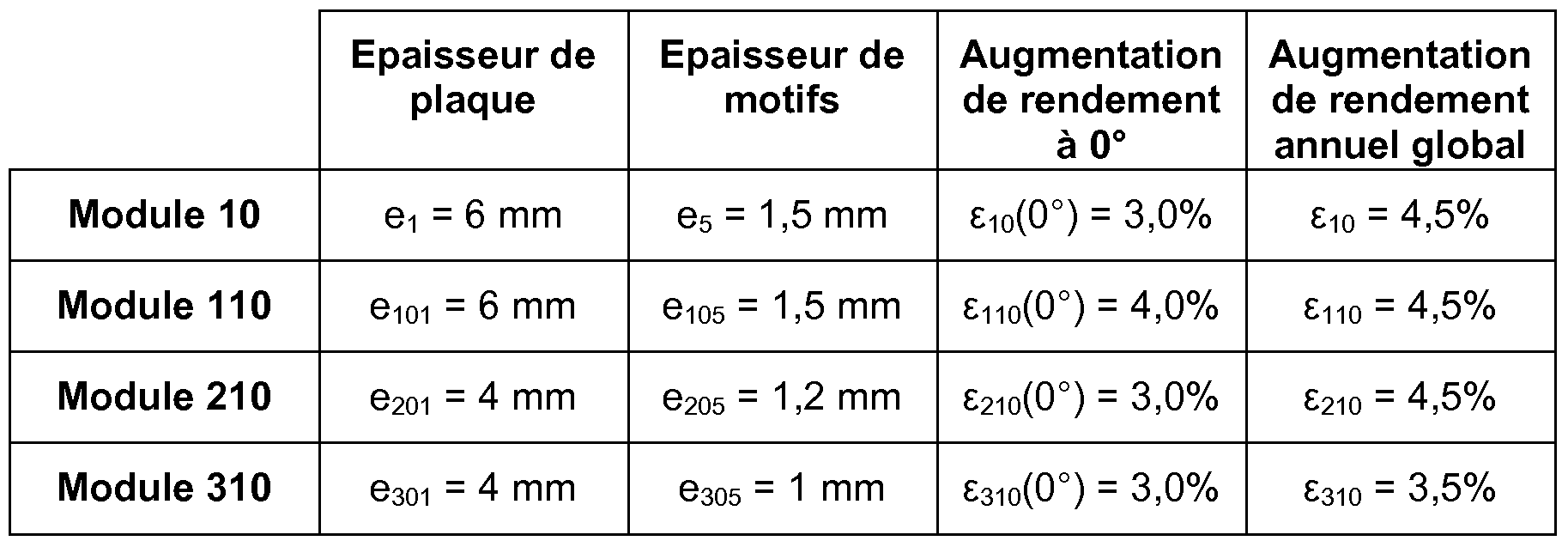
- Table 1 below illustrates the increase of the yield at zero incidence angle, ⁇ i (O °), ⁇ no (O °), £ 210 (0 °) and £ 310 (0 °), and the overall annual yield. for all angles of incidence, ⁇ io, £ no, £ 210 and ⁇ 3 i 0 , respectively of module 10, the module 110, the module 210 and the module 310, with respect to the performance of a reference photovoltaic module, determined by optical simulation of the surface structures of the plates 1, 101, 201 and 301.
- the reference module differs modules 10, 110, 210, 310 only in that its front substrate is a non-textured transparent plate of the same glass composition as the textured plates 1, 101, 201 and 301.
- the results can be transposed to other types of photovoltaic cells, since the improvement of the transmission properties of a plate due to the texturing of this plate does not depend significantly on the wavelength of the incident radiation on the plate.
- the first principle underlying the increase in transmission for a textured plate is the trapping of the incident radiation due to multiple reflections on the relief patterns of the plate.
- FIGS. 2 to 5 for incident rays E 1 on the plate 1, 101, 201, 301 of low angles of incidence, multiple reflections occur on the patterns 5, 105, 205, 305.
- relief of the textured face 3, 103, 203, 303 which give the radiation a number of possibilities En, E t2 more important to enter the plate, resulting in a reduction of the reflection on the textured face 3, 103, 203 , 303 of the plate 1, 101, 201, 301 with respect to the flat face of a non-textured plate.
- this reduction in the area of the bonding zones is obtained by increasing the thickness of the patterns of the plate relative to the patterns of the plates of the state of the art, so that the area of each pattern between two adjacent bonding areas, which is the area or surface of the pattern useful for multiple reflections on the pattern, is higher.
- the radiation is reflected, after entering the plate 1, 101, 201, 301, at the interface between the plate and the cells 9, 109, 209, 309 or a possible lamination interlayer, and is trapped at again by reflection on the faces of the patterns 5, 105, 205, 305, so that a larger portion of the radiation is transmitted through the plate.
- the reflection losses are thus further reduced, for a textured plate compared to a non-textured plate, thanks to this second trapping of the radiation.
- the decrease in the area of the bonding areas 8, 108, 208, 308 relative to the total textured area of the plate, or in other words the increase in the effective area of each pattern to multiple reflections on the pattern increases the second trapping of the radiation and its transmission through the plate.
- the second principle underlying the transmission increase for a textured plate is that, for F-rays, incident on the plate of high angles of incidence, greater than 45 °, the radiation has angles of lower incidence on the faces of the patterns 5, 105, 205, 305 than on a flat surface.
- the radiation has angles of lower incidence on the faces of the patterns 5, 105, 205, 305 than on a flat surface.
- incident rays F 1 incidence angle varying between 0 and 90 ° on a flat surface meet the surface of the texture 5, 105 with an angle of incidence between -45 ° and + 45 °.
- a plate according to the invention including the ratio of the area S 8 , SiO 2 , S 2 O 8 binding areas on the total textured area Si , S101, S201 of the plate has been reduced compared to that of the plates of the state of the art, has optimized properties of transmitting incident radiation on the plate. Therefore, such a plate, when integrated in a photovoltaic module as a front substrate, significantly improves the efficiency of this module compared to the yields of the modules of the state of the art.
- the improvement of the transmission through the textured plate is obtained, according to the invention, by increasing the area or the effective area of the patterns of the plate, that is to say the surface of the patterns which is useful for receiving and transmitting radiation, whether by multiple reflections or by decreasing the angle of incidence as seen by the surface of the pattern. In doing so, the percentage of the total textured area of the plate corresponding to rounded bonding areas is decreased and a perfect geometrical profile of the patterns of the textured plate is approached.
- the invention proposes to increase the thickness of the textured plate according to the invention with respect to the thickness of the textured plates of the state of the art for a given value.
- the ratio p of the thickness of each pattern to the thickness of the plate as illustrated in the first and second embodiments. It emerges from these embodiments that the transmission of radiation through the textured plate according to the invention is improved with respect to the transmission of radiation through the textured plates of the state of the art, even though the thickness of the plate according to the invention, and therefore the absorption of radiation in the plate is higher.
- the inventors have demonstrated that the increase in transmission through the textured plate according to the invention, which is induced by the increase in the thickness of the patterns and therefore the useful surface of these patterns, is likely, for some values of the thickness of the plate, to be greater than the increase in the absorption of radiation inside the plate, which is induced by the increase in the thickness of the plate. plate, in particular for a composition of the plate with low radiation absorption.
- the value of the thickness of the textured plate according to the invention is preferably chosen to be equal to an optimum thickness value for which the increase in transmission through the plate, due to the increase in the thickness of the patterns counterbalances at best the increase in the absorption in the plate, due to the increase in the thickness of the plate, that is to say for which the transmission through the plate of incident radiation on the textured face of the plate is maximum.
- the thickness of the textured plate according to the invention is preferably chosen greater than or equal to 4.5 mm.
- the thickness of a textured plate according to the invention is preferably also kept lower or 8 mm, in order to maintain a moderate weight of the device.
- Another solution for increasing the usable area of the patterns consists, as illustrated in the third embodiment, of increasing the ratio p of the thickness of each pattern to the thickness of the plate with respect to the ratio p of the textured plates of the plate. state of the art for a given value of the thickness of the plate.
- the useful area of the patterns for receiving and transmitting radiation is then increased by increasing the thickness of each pattern.
- the ratio p of the textured plate according to the invention is preferably chosen such that 0.3 ⁇ p.
- a maximum value p 0.5 is imposed in practice because of the rolling process, in order to avoid problems of bonding the glass to the rolling rolls. .
- the invention is based on the demonstration by the inventors that the conventional manufacturing processes of textured plates that are rolling and molding induce radii of curvature at the recesses and vertices of the patterns in relief, which do not change. whatever the thickness of the patterns and the thickness of the plate. It might have been thought that these radii of curvature would increase homothetically with the thickness of the patterns and the thickness of the plate. Surprisingly, the average radii of curvature remain the same for a given manufacturing process by rolling or molding, in particular of the order of a few hundred microns for the radii of curvature r and R in the case of rolling.
- the inventors have taken advantage of this stability of the radii of curvature to obtain a more effective texturing in terms of increasing the transmission through the textured plate.
- they have chosen, for this purpose, to increase the plate thickness for a value of the given ratio p.
- the texturing of a plate according to the invention may be formed by an assembly of patterns other than pyramidal patterns.
- the patterns of a plate according to the invention may in particular be cones, or elongated patterns of the groove or rib type.
- these patterns are advantageously polygonal, including triangular, square, rectangular, parallelogram, hexagonal or octagonal.
- the patterns of a plate according to the invention are such that they comprise at least two sidewalls inclined with respect to a general plane ⁇ of the face of the plate comprising the patterns.
- the angle of inclination of a flank by relative to the general plane ⁇ is defined as a mean angle of inclination delimited between an average surface of the sidewall and the plane ⁇ .
- the texturing of a plate according to the invention may also be a concave texturing, instead of a convex texturing, the patterns then being hollow relative to the general plane of the textured face of the plate.
- the patterns of a plate according to the invention if they are preferably contiguous, can also be non-contiguous. Likewise, a random pattern distribution on the textured face of the plate, if advantageous, is not required.
- the patterns of a textured plate according to the invention may be identical to each other, as in the embodiments described above, or different from each other.
- the patterns of a plate according to the invention may be formed on the entire surface of the corresponding face of the plate or, alternatively, only on a region or several distinct regions of this surface.
- a textured plate according to the invention may be made of an extra-clear transparent glass of any composition, in particular "ALBARINO” glass or an extra-clear transparent float glass such as the glass marketed in the "DIAMOND” range. by Saint-Gobain Glass.
- the texturing by rolling can be carried out by means of a texturing roller integrated in a glass floating device.
- a textured plate according to the invention may also be made of a transparent material other than glass, for example a transparent thermoplastic polymer, such as polycarbonate or polymethylmethacrylate.
- a plate according to the invention may also include texturing on both sides, and not only on one of its faces as in the examples described and shown.
- an advantageous application of a textured plate according to the invention, having optimized properties for transmitting incident radiation, is its use as a front substrate for an energy conversion device, such as a module photovoltaic system, a thermal module or an OLED device.
- a textured plate according to the invention can also be used as decorative glazing element.
Landscapes
- Physics & Mathematics (AREA)
- Optics & Photonics (AREA)
- General Physics & Mathematics (AREA)
- Photovoltaic Devices (AREA)
- Shaping Of Tube Ends By Bending Or Straightening (AREA)
- Optical Elements Other Than Lenses (AREA)
- Laminated Bodies (AREA)
- Moulds For Moulding Plastics Or The Like (AREA)
Abstract
Description
Claims
Priority Applications (6)
| Application Number | Priority Date | Filing Date | Title |
|---|---|---|---|
| MX2012000722A MX341629B (es) | 2009-07-16 | 2010-07-15 | Placa transparente texturada y procedimiento de fabricacion de tal placa. |
| KR1020177013364A KR20170058455A (ko) | 2009-07-16 | 2010-07-15 | 텍스처된 투명판 및 그러한 판의 제조 방법 |
| JP2012520036A JP2012533096A (ja) | 2009-07-16 | 2010-07-15 | 凹凸付き透明板及びそのような板の製造方法 |
| CN201080041913.8A CN102576742B (zh) | 2009-07-16 | 2010-07-15 | 带纹理的透明板和这种板的制造方法 |
| US13/384,406 US9257580B2 (en) | 2009-07-16 | 2010-07-15 | Textured transparent plate and method of manufacturing such a plate |
| EP10730808A EP2454757A2 (fr) | 2009-07-16 | 2010-07-15 | Plaque transparente texturee et procede de fabrication d'une telle plaque |
Applications Claiming Priority (2)
| Application Number | Priority Date | Filing Date | Title |
|---|---|---|---|
| FR0954908A FR2948230B1 (fr) | 2009-07-16 | 2009-07-16 | Plaque transparente texturee et procede de fabrication d'une telle plaque |
| FR0954908 | 2009-07-16 |
Publications (2)
| Publication Number | Publication Date |
|---|---|
| WO2011006957A2 true WO2011006957A2 (fr) | 2011-01-20 |
| WO2011006957A3 WO2011006957A3 (fr) | 2012-03-08 |
Family
ID=42111042
Family Applications (1)
| Application Number | Title | Priority Date | Filing Date |
|---|---|---|---|
| PCT/EP2010/060199 Ceased WO2011006957A2 (fr) | 2009-07-16 | 2010-07-15 | Plaque transparente texturee et procede de fabrication d'une telle plaque |
Country Status (8)
| Country | Link |
|---|---|
| US (1) | US9257580B2 (fr) |
| EP (1) | EP2454757A2 (fr) |
| JP (3) | JP2012533096A (fr) |
| KR (2) | KR20120049265A (fr) |
| CN (1) | CN102576742B (fr) |
| FR (1) | FR2948230B1 (fr) |
| MX (1) | MX341629B (fr) |
| WO (1) | WO2011006957A2 (fr) |
Cited By (3)
| Publication number | Priority date | Publication date | Assignee | Title |
|---|---|---|---|---|
| WO2013061099A1 (fr) * | 2011-10-27 | 2013-05-02 | Christophoros Diakopoulos | Panneaux photovoltaïques à haut rendement énergétique |
| WO2016170261A1 (fr) * | 2015-04-23 | 2016-10-27 | Saint-Gobain Glass France | Verre texture pour serre |
| US20210313480A1 (en) * | 2018-07-27 | 2021-10-07 | (Cnbm) Bengbu Design & Research Institute For Glass Industry Co., Ltd | Solar module with patterned cover plate and optical interference layer |
Families Citing this family (7)
| Publication number | Priority date | Publication date | Assignee | Title |
|---|---|---|---|---|
| US9876129B2 (en) * | 2012-05-10 | 2018-01-23 | International Business Machines Corporation | Cone-shaped holes for high efficiency thin film solar cells |
| JP6186377B2 (ja) | 2012-12-18 | 2017-08-23 | パイオニア株式会社 | 発光装置 |
| CN103824967A (zh) * | 2013-12-30 | 2014-05-28 | 北京维信诺科技有限公司 | 一种具有内光取出结构的基板及其制造方法 |
| US20150285959A1 (en) * | 2014-04-02 | 2015-10-08 | Nebula Energy Inc. | Solar radiation concentrators, methods of concentrating solar radiation, and solar radiation concentrating prism lenses |
| WO2017217303A1 (fr) * | 2016-06-14 | 2017-12-21 | ミネベアミツミ株式会社 | Élément de commande de distribution de lumière et dispositif d'éclairage. |
| EP3599318B1 (fr) * | 2018-07-27 | 2021-11-10 | (CNBM) Bengbu Design & Research Institute for Glass Industry Co., Ltd. | Éléments de façade pourvus de plaque de couverture structurée et de couche d'interférence optique |
| ES2928504T3 (es) * | 2020-01-28 | 2022-11-18 | Cnbm Res Institute For Advanced Glass Materials Group Co Ltd | Elemento de fachada coloreado con estructura de paneles compuestos |
Citations (4)
| Publication number | Priority date | Publication date | Assignee | Title |
|---|---|---|---|---|
| WO2003046617A1 (fr) | 2001-11-28 | 2003-06-05 | Saint-Gobain Glass France | Plaque transparente texturee a forte transmission de lumiere |
| WO2005111670A1 (fr) | 2004-05-10 | 2005-11-24 | Saint-Gobain Glass France | Feuille transparente texturee a motifs pyramidaux qui peut etre associee a des cellules photovoltaiques |
| WO2006134301A2 (fr) | 2005-06-16 | 2006-12-21 | Saint-Gobain Glass France | Vitre transparente dotée d'une structure de surface |
| WO2007015019A1 (fr) | 2005-08-02 | 2007-02-08 | Saint-Gobain Glass France | Plaque texturee a motifs asymetriques |
Family Cites Families (13)
| Publication number | Priority date | Publication date | Assignee | Title |
|---|---|---|---|---|
| DE19514908C1 (de) * | 1995-04-22 | 1996-04-18 | Ver Glaswerke Gmbh | Verfahren zur Herstellung eines Solarmoduls |
| JP2003279705A (ja) * | 2002-03-25 | 2003-10-02 | Sanyo Electric Co Ltd | 反射防止部材 |
| NL1025191C2 (nl) * | 2004-01-08 | 2005-07-11 | Agrotechnology And Food Innova | Afdekking voor een zonnestraling gebruikend object. |
| CN1942788A (zh) * | 2004-02-26 | 2007-04-04 | 他喜龙株式会社 | 光扩散片和使用该光扩散片的背光单元 |
| FR2881844B1 (fr) | 2005-02-09 | 2007-04-13 | Saint Gobain | Structure diffusante a proprietes d'absorption dans l'ultraviolet |
| DE102005027737B4 (de) | 2005-06-16 | 2013-03-28 | Saint-Gobain Glass Deutschland Gmbh | Verwendung einer transparenten Scheibe mit einer dreidimensionalen Oberflächenstruktur als Deckscheibe für Bauelemente zur Nutzung des Sonnenlichts |
| JP4662151B2 (ja) * | 2005-11-29 | 2011-03-30 | 大日本印刷株式会社 | 太陽電池モジュール用充填材、およびそれを用いた太陽電池モジュール、ならびに太陽電池モジュール用充填材の製造方法 |
| JP2008241889A (ja) * | 2007-03-26 | 2008-10-09 | Sekisui Chem Co Ltd | プリズムシート及び光学シート |
| FR2915834B1 (fr) | 2007-05-04 | 2009-12-18 | Saint Gobain | Substrat transparent muni d'une couche electrode perfectionnee |
| FR2916901B1 (fr) | 2007-05-31 | 2009-07-17 | Saint Gobain | Procede d'obtention d'un substrat texture pour panneau photovoltaique |
| FR2917899B1 (fr) * | 2007-06-21 | 2010-05-28 | Apollon Solar | Module photovoltaique comprenant un film polymere et procede de fabrication d'un tel module |
| FR2938078B1 (fr) | 2008-11-03 | 2011-02-11 | Saint Gobain | Vitrage a zones concentrant la lumiere par echange ionique. |
| FR2941447B1 (fr) | 2009-01-23 | 2012-04-06 | Saint Gobain | Substrat en verre transparent et procede de fabrication d'un tel substrat. |
-
2009
- 2009-07-16 FR FR0954908A patent/FR2948230B1/fr active Active
-
2010
- 2010-07-15 KR KR1020127003951A patent/KR20120049265A/ko not_active Ceased
- 2010-07-15 JP JP2012520036A patent/JP2012533096A/ja active Pending
- 2010-07-15 MX MX2012000722A patent/MX341629B/es active IP Right Grant
- 2010-07-15 WO PCT/EP2010/060199 patent/WO2011006957A2/fr not_active Ceased
- 2010-07-15 CN CN201080041913.8A patent/CN102576742B/zh not_active Expired - Fee Related
- 2010-07-15 US US13/384,406 patent/US9257580B2/en not_active Expired - Fee Related
- 2010-07-15 KR KR1020177013364A patent/KR20170058455A/ko not_active Ceased
- 2010-07-15 EP EP10730808A patent/EP2454757A2/fr not_active Withdrawn
-
2015
- 2015-06-03 JP JP2015113282A patent/JP2015172777A/ja active Pending
-
2017
- 2017-11-06 JP JP2017005048U patent/JP3214571U/ja not_active Expired - Lifetime
Patent Citations (4)
| Publication number | Priority date | Publication date | Assignee | Title |
|---|---|---|---|---|
| WO2003046617A1 (fr) | 2001-11-28 | 2003-06-05 | Saint-Gobain Glass France | Plaque transparente texturee a forte transmission de lumiere |
| WO2005111670A1 (fr) | 2004-05-10 | 2005-11-24 | Saint-Gobain Glass France | Feuille transparente texturee a motifs pyramidaux qui peut etre associee a des cellules photovoltaiques |
| WO2006134301A2 (fr) | 2005-06-16 | 2006-12-21 | Saint-Gobain Glass France | Vitre transparente dotée d'une structure de surface |
| WO2007015019A1 (fr) | 2005-08-02 | 2007-02-08 | Saint-Gobain Glass France | Plaque texturee a motifs asymetriques |
Non-Patent Citations (1)
| Title |
|---|
| See also references of EP2454757A2 |
Cited By (8)
| Publication number | Priority date | Publication date | Assignee | Title |
|---|---|---|---|---|
| WO2013061099A1 (fr) * | 2011-10-27 | 2013-05-02 | Christophoros Diakopoulos | Panneaux photovoltaïques à haut rendement énergétique |
| WO2016170261A1 (fr) * | 2015-04-23 | 2016-10-27 | Saint-Gobain Glass France | Verre texture pour serre |
| FR3035398A1 (fr) * | 2015-04-23 | 2016-10-28 | Saint Gobain | Verre texture pour serre |
| US10246363B2 (en) | 2015-04-23 | 2019-04-02 | Saint-Gobain Glass France | Textured glass for greenhouses |
| RU2696907C2 (ru) * | 2015-04-23 | 2019-08-07 | Сэн-Гобэн Гласс Франс | Текстурированное стекло для теплиц |
| RU2696907C9 (ru) * | 2015-04-23 | 2020-01-28 | Сэн-Гобэн Гласс Франс | Текстурированное стекло для теплиц |
| US20210313480A1 (en) * | 2018-07-27 | 2021-10-07 | (Cnbm) Bengbu Design & Research Institute For Glass Industry Co., Ltd | Solar module with patterned cover plate and optical interference layer |
| US12464853B2 (en) * | 2018-07-27 | 2025-11-04 | Cnbm Research Institute For Advanced Glass Materials Group Co., Ltd. | Solar module with patterned cover plate and optical interference layer |
Also Published As
| Publication number | Publication date |
|---|---|
| MX341629B (es) | 2016-08-29 |
| FR2948230A1 (fr) | 2011-01-21 |
| FR2948230B1 (fr) | 2011-10-21 |
| WO2011006957A3 (fr) | 2012-03-08 |
| CN102576742A (zh) | 2012-07-11 |
| JP2012533096A (ja) | 2012-12-20 |
| KR20170058455A (ko) | 2017-05-26 |
| MX2012000722A (es) | 2012-03-26 |
| CN102576742B (zh) | 2015-05-13 |
| US9257580B2 (en) | 2016-02-09 |
| KR20120049265A (ko) | 2012-05-16 |
| JP2015172777A (ja) | 2015-10-01 |
| EP2454757A2 (fr) | 2012-05-23 |
| JP3214571U (ja) | 2018-01-25 |
| US20120183734A1 (en) | 2012-07-19 |
Similar Documents
| Publication | Publication Date | Title |
|---|---|---|
| WO2011006957A2 (fr) | Plaque transparente texturee et procede de fabrication d'une telle plaque | |
| EP2227829B1 (fr) | Perfectionnements apportes a des elements capables de collecter de la lumiere | |
| EP1449017B1 (fr) | Plaque transparente texturee a forte transmission de lumiere | |
| WO2008152300A2 (fr) | Procede d'obtention d'un substrat texture pour panneau photovoltaïque | |
| EP1774372B1 (fr) | Feuille transparente texturee a motifs pyramidaux qui peut être associée à des cellules photovoltaiques | |
| WO2010084290A1 (fr) | Substrat en verre transparent et procede de fabrication d'un tel substrat | |
| WO2008148978A2 (fr) | Substrat transparent muni d'une couche electrode perfectionnee | |
| JP4903314B2 (ja) | 薄膜結晶質Si太陽電池 | |
| EP2190024A1 (fr) | Dispositif photoélectrique a jonctions multiples et son procédé de realisation | |
| EP4128365B1 (fr) | Bipv integrant un element transparent ou translucide a reflexion diffuse | |
| EP3152787B1 (fr) | Dispositif photovoltaïque et procédé de fabrication associé | |
| US20120192933A1 (en) | Light-trapping layer for thin-film silicon solar cells | |
| EP3000136B1 (fr) | Procédé de fabrication d'un système photovoltaïque à concentration de lumière | |
| FR3143856A1 (fr) | Procédé de fabrication d’une cellule photovoltaïque | |
| EP4192795A1 (fr) | Verre texture pour installation photovoltaique | |
| EP2461362A1 (fr) | Panneau solaire photovoltaïque à diodes en couches minces | |
| FR2948498A1 (fr) | Panneau solaire photovoltaique a diodes en couches minces | |
| JP2006019481A (ja) | 薄膜太陽電池の製造方法およびその方法により製造した薄膜太陽電池 | |
| JP2010073864A (ja) | 太陽電池モジュール |
Legal Events
| Date | Code | Title | Description |
|---|---|---|---|
| WWE | Wipo information: entry into national phase |
Ref document number: 201080041913.8 Country of ref document: CN |
|
| 121 | Ep: the epo has been informed by wipo that ep was designated in this application |
Ref document number: 10730808 Country of ref document: EP Kind code of ref document: A2 |
|
| NENP | Non-entry into the national phase |
Ref country code: DE |
|
| WWE | Wipo information: entry into national phase |
Ref document number: 2012520036 Country of ref document: JP Ref document number: MX/A/2012/000722 Country of ref document: MX |
|
| WWE | Wipo information: entry into national phase |
Ref document number: 593/CHENP/2012 Country of ref document: IN |
|
| WWE | Wipo information: entry into national phase |
Ref document number: 2010730808 Country of ref document: EP |
|
| ENP | Entry into the national phase |
Ref document number: 20127003951 Country of ref document: KR Kind code of ref document: A |
|
| WWE | Wipo information: entry into national phase |
Ref document number: 13384406 Country of ref document: US |