WO2011024654A1 - 画像処理装置及び画像処理方法 - Google Patents
画像処理装置及び画像処理方法 Download PDFInfo
- Publication number
- WO2011024654A1 WO2011024654A1 PCT/JP2010/063740 JP2010063740W WO2011024654A1 WO 2011024654 A1 WO2011024654 A1 WO 2011024654A1 JP 2010063740 W JP2010063740 W JP 2010063740W WO 2011024654 A1 WO2011024654 A1 WO 2011024654A1
- Authority
- WO
- WIPO (PCT)
- Prior art keywords
- image processing
- memory
- parallel
- image
- cpu
- Prior art date
- Legal status (The legal status is an assumption and is not a legal conclusion. Google has not performed a legal analysis and makes no representation as to the accuracy of the status listed.)
- Ceased
Links
Images

Classifications
-
- G—PHYSICS
- G06—COMPUTING OR CALCULATING; COUNTING
- G06T—IMAGE DATA PROCESSING OR GENERATION, IN GENERAL
- G06T1/00—General purpose image data processing
- G06T1/20—Processor architectures; Processor configuration, e.g. pipelining
Definitions
- the present invention relates to an apparatus and method suitable for high-speed image processing.
- Non-Patent Documents 1 to 5 below since high-speed vision enables stable visual feedback control, high-speed vision is applied to control robots that require high-speed operation.
- Non-patent Documents 6 and 7 below since high-speed vision can measure fast movement, it is applied to living body observation (Non-patent Documents 6 and 7 below), motion capture (Non-patent Document 8 below), fluid measurement (Non-patent Document 9 below), and the like. ing.
- tracking (the following non-patent documents 10 and 11), three-dimensional measurement (the following non-patent documents 12 and 13), image synthesis (the following non-patent documents 14 and 15), optical flow estimation (the following non-patent document 16), and the like
- image synthesis (the following non-patent documents 14 and 15)
- optical flow estimation (the following non-patent document 16), and the like
- Non-Patent Document 10 SIMD type massively parallel processors
- FPGA Field Programmable Gate Array
- Non-Patent Documents 19 to 22 below Non-Patent Documents 19 to 22 below.
- PE processing elements
- the focal plane processor that performs arithmetic processing on the imaging surface of the image sensor can also be said to be suitable for high frame rate processing, but due to restrictions on the circuit area, many are made specifically for specific processing.
- a general-purpose arithmetic unit has been developed (Non-Patent Documents 23 to 26 below), but has the same problem as the above SIMD type massively parallel processor.
- Non-patent Documents 27 and 28 below DSPs employing parallel processing technologies such as VLIW (Very Long Long Instruction Word) and multi-core have appeared, and high-speed processing is possible (Non-patent Documents 27 and 28 below).
- VLIW Very Long Long Instruction Word
- the parallelization of the algorithm is mainly performed automatically by the compiler, so the time required to execute the instruction can be predicted in advance, or the execution speed decreases due to an unexpected reason.
- ASIC and FPGA can implement the parallelism of the algorithm as it is in hardware, so the efficiency of parallelization is high and the processing is easy to optimize.
- FPGAs which are LSIs with rewritable hardware configurations, are particularly suitable for prototypes and small-scale production.
- a system using an FPGA requires a circuit design based on HDL (Hardware Description Language) every time an algorithm is changed, and has a problem of high development cost.
- HDL Hardware Description Language
- Non-patent Document 29 a system that can customize the instruction set of a general-purpose CPU using the reconfigurability of the FPGA has also been proposed (Non-patent Document 29 below).
- This system combines the ease of software development of the CPU with the reconfigurability of the FPGA, minimizing the burden of circuit design for the user.
- this system only CPUs prepared in advance can be used, and commercial development tools, middleware, software assets, etc. cannot be utilized to the maximum extent.
- the CPU and the FPGA are separated as much as possible and the FPGA operates autonomously considering the performance degradation due to interrupts and multitasking.
- a mechanism for parallel processing, parallel data access, and high-speed data transfer required for image processing is prepared in advance.
- a main object of the present invention is to speed up image processing by operating a plurality of image processing units corresponding to a specific function for image processing by a program.
- a coprocessor a frame memory, and a CPU;
- the frame memory is configured to store image data to be processed,
- the coprocessor includes a plurality of image processing units and a plurality of parallel memories,
- the parallel memory is configured to receive all or part of the image data stored in the frame memory and send it to any of the image processing units,
- Each of the plurality of image processing units has a function corresponding to a function for image processing,
- the plurality of image processing units according to the command from the CPU, Receiving all or part of the image data from the parallel memory or the frame memory;
- An image processing apparatus configured to perform processing according to a function for image processing on all or part of the image data.
- the image processing unit corresponds to a specific function used for image processing.
- image processing it is possible to speed up the processing by executing a function necessary for the processing by a dedicated image processing unit.
- a specific function or an image processing unit can be designated and executed through the CPU.
- Reconfigurable programmable logic devices are usually integrated circuits called FPGAs or FPLAs.
- FPGAs field-programmable logic arrays
- FPLAs field-programmable logic arrays
- Using a dual port memory allows reading and writing to the memory independently. For this reason, it is possible to further speed up the processing.
- the image processing unit includes a direct memory access controller and a processing unit,
- the direct memory access controller is configured to control the operation of the parallel memory,
- the image processing apparatus according to any one of items 1 to 3, wherein the processing unit is configured to perform processing according to a function for the image processing.
- the coprocessor further comprises a descriptor,
- the CPU is configured to write an instruction to the coprocessor to the descriptor,
- the image processing device according to any one of items 1 to 6, wherein the coprocessor is configured to read an instruction written in the descriptor and execute processing by the plurality of image processing units.
- the CPU can instruct the coprocessor to perform a plurality of processes at a time. For this reason, there is an advantage that the number of interruptions to the CPU when the operation of the coprocessor is completed can be reduced.
- An image processing method comprising the following steps: (1) a step in which the frame memory stores image data to be processed; (2) a parallel memory receiving all or part of the image data stored in the frame memory; (3) The plurality of image processing units receiving all or part of the image data from the parallel memory or the frame memory in accordance with a command from the CPU; (4) A step in which the plurality of image processing units respectively perform processing according to a function for image processing on all or a part of the image data in accordance with an instruction from the CPU.
- a dual port memory is used as the parallel memory, The image processing method according to item 9, wherein the plurality of image processing units perform pipeline processing using the parallel memory as a buffer in accordance with a command from the CPU.
- Image processing can be further speeded up by performing pipeline processing using parallel memory as a buffer.
- the plurality of image processing units are configured to operate independently and in parallel according to a command from the CPU, The image processing method according to item 9 or 10, wherein the plurality of image processing units perform parallel processing at a task level in accordance with a command from the CPU.
- Acceleration of image processing can be achieved by performing parallel processing at the task level.
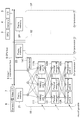
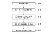
- FIG. 1 is a schematic block diagram of an image processing apparatus according to an embodiment of the present invention. It is a flowchart which shows the outline of the image processing method using the apparatus of FIG. It is a schematic hardware block diagram in the apparatus of FIG.
- This image processing apparatus includes P coprocessors 11, 12,..., 1 P, P frame memories 21, 22,.
- the apparatus further includes a main memory 4, an I / O interface 5, a camera interface 6, a video interface 7, a CPU bus 8, and an intercoprocessor bus 9.
- Each frame memory 21 is configured to store image data to be processed. Specifically, in this embodiment, the image data captured from the camera interface 6 or the video interface 7 is stored. As shown in the figure, each frame memory 21 is provided corresponding to each coprocessor 11.
- Each of the coprocessors 11 ..., a plurality of direct memory access controllers (DMAC) 111, 112, ..., 11N, a plurality of parallel memories 121, 122, ..., 12M, and a plurality of processing units 13A, 13B. ,... 13X. Since the basic internal configuration of each coprocessor is the same in this embodiment, only the internal configuration of the coprocessor 11 will be described in detail.
- DMAC direct memory access controllers
- the DMACs 111 and the processing units 13A constitute a plurality of image processing units in the present invention.
- the DMAC and the processing unit do not correspond one-to-one.
- the DMACs 111 are responsible for the image processing function, it is also possible to grasp that there are a plurality of image processing units when there are a plurality of DMACs.
- the DMACs 111 are configured to control the operation of the parallel memories 121. However, in this embodiment, the DMAC 111 is further assigned to the processing units 13A to execute an image processing function.
- the processing unit 13A has a configuration corresponding to a function for image processing.
- the parallel memory 121 Is configured to receive all or part of the image data stored in the frame memory 21 and send it to one of the processing units 13A via the DMAC.
- a dual port memory is used as the parallel memory 121 in this embodiment.
- the plurality of DMACs 111 and the processing unit units 13A in the present embodiment all have a function corresponding to a function for image processing. However, a configuration in which only this processing unit 13A.
- the DMAC 111 and the processing unit unit 13A are configured to receive all or part of the image data from the parallel memory 121 or the frame memory 21 in accordance with a command from the CPU 3. Further, the DMACs 111 and the processing unit units 13A are configured to perform processing according to a function for image processing on all or part of the image data.
- the coprocessor 11 in this embodiment is configured by a reconfigurable programmable logic device, that is, a so-called FPGA. Accordingly, the number and capacity of the parallel memories 121 in the coprocessors 11 and the number and function of the DMACs 111 and the processing units 13A can be changed by rewriting the coprocessors 11.
- the I / O interface 5 is a part that controls input / output operations with an external device (not shown).
- the camera interface 6 has a function for capturing an image from a camera (not shown).
- the video interface 7 has a function for capturing an image from a video (not shown).
- the CPU bus 8 is a bus for transferring data between the CPU 3 and each coprocessor 11.
- the intercoprocessor bus 9 is a bus for transferring data between the coprocessors 11.
- Each coprocessor 11 is further provided with a descriptor 141.
- the descriptor 141 is a register array for writing the contents of image processing and direct memory access (DMA) in accordance with a command from the CPU 3. That is, the CPU 3 according to the present embodiment is configured to write an instruction for the coprocessors 11 to the descriptor 141.
- DMA direct memory access
- the coprocessor 11 is configured to read an instruction written in the descriptor 141 and execute processing by the DMAC 111 and processing units 13A (that is, processing by a plurality of image processing units).
- Step S-1 in FIG. 2 First, an image to be processed is fetched from the camera interface 6 or the video interface 7 in accordance with an instruction from the CPU 3.
- Step S-2 in FIG. 2 the frame memory 21 corresponding to the coprocessor 11 that processes the image stores the image or a part thereof. This process is also performed by an instruction from the CPU 3.
- the CPU 3 writes a command for each coprocessor 11... Into each descriptor 141.
- the CPU 3 writes the following information (command) in each descriptor 141.
- Step S-3 in FIG. 2 Then, each coprocessor 11... Reads the command written in the descriptor 141.
- each coprocessor 11 Reads the command written in the descriptor 141 and assigns processing to each image processing unit (DMAC and processing unit).
- DMAC and processing unit operates independently and in parallel. For example, it is possible to perform coordinate transformation while performing the summation calculation.
- the coprocessor can be instructed to perform multiple processes at once, so the number of interrupts to the CPU when the coprocessor operation is completed can be reduced.
- Step S-4 and Step S-5 in FIG. 2 the image processing unit receives and processes all or part of the image from the frame memory 21 or the parallel memory 121. This process is described in detail below.
- a module that distributes the processing written in the descriptor (this module can be built in the descriptor, for example) operates as follows.
- the processing unit includes a DMAC (when it has an image processing function). 1) Read the next descriptor. 2) If the descriptor is empty, stop processing. 3) Wait until all processing units to be used and all waiting units are available. 4) Distribute processing to processing units. 5) Return to 1) above.
- the algorithm can be implemented using only a normal CPU programming environment.
- Processing units 13 ⁇ / b> A for performing basic image processing, or DMAC 111... are prepared in advance, and various algorithms can be implemented by using them in combination.
- image processing can be performed at high speed.
- an instruction can be written to the descriptor by calling an API (Application Programming Interface) prepared in the program.
- API Application Programming Interface
- the function proc_X takes the following format.
- the function name represents the type of processing.
- cp indicates a coprocessor to be used
- unit indicates a processing unit to be used
- wunit indicates a waiting unit.
- the memory to be used, address, image size, calculation parameters, etc. are also specified by arguments.
- sync () When sync () is called, the firmware waits until the specified processing unit becomes available.
- the argument of sync () takes the coprocessor cp to be used and the wait unit wunit.
- the processing unit 13A is mounted by a dedicated circuit for each process, and is executed simultaneously by operations and parallelized by a pipeline. In addition, by simultaneously reading a plurality of data from the parallel memories 121, it is possible to perform processing for one pixel or more in one clock. These can be regarded as parallel processing within a task.
- parallel processing at a task level can be performed according to a command (that is, a program) from the CPU using a plurality of image processing units operating in parallel.
- the memory outside the FPGA such as PBSRAM (described later) and frame memory, is generally equipped with an arbitration function and can be accessed simultaneously.
- ⁇ A method to divide one image and execute each in a separate unit, ⁇
- ⁇ When performing the same process multiple times, such as template matching, to execute them in separate units, -There is a method of pipeline processing at the task level.
- the parallel memory 121 when configured with a dual port RAM, reading and writing can be performed independently. Therefore, even if the output destination of the process is the input source of the next process, if it can be guaranteed that the subsequent process will not overtake the previous process, the next process will be completed before all the processes are completed. Can start.
- Fig. 3 shows a block diagram of the developed system. This system is mounted on one main board on which two sub boards are mounted.
- the main board is equipped with FPGA, memory, I / O ports, etc.
- the sub board is CPU board and camera interface board.
- -FPGA Coprocessor-DDR2DIMM: Frame memory-DIO, USB, RS-232C, Ethernet (registered trademark): I / O interface-DDR-SDRAM: Main memory-EXT.BUS: Expansion bus
- each FPGA is connected to the CPU bus via this expansion bus. Therefore, in terms of function, this expansion bus serves as a bus between coprocessors and a CPU bus.
- PBSRAM in FIG. 3 is an external memory for each FPGA.
- the CPU board uses a commercially available CPU board ESPT-Giga (trade name) and is connected to the FPGA in the main board through the expansion bus.
- ESPT-Giga is equipped with Renesas SH7763 (SH-4A, 266MHz) in CPU, 64MB DDR-SDRAM in memory, and 10/100 / 1000BASE Ethernet (registered trademark), USB1.1, RS232C as input / output I have.
- ESPT-Giga can incorporate a web server function, and can operate the system from a PC through a browser and display processing results.
- remote management by LAN is possible, and many systems can be managed by a single PC.
- PBSRAM is a flash memory (8 MBytes) for storing FPGA configuration data, which is installed in each FPGA.
- Each FPGA has a frame memory (DRAM), and the input image from the camera is automatically stored in the frame memory of FPGA1.
- the camera interface is connected to FPGA1.
- a physical interface for an individual camera is mounted and used on a camera interface board mounted on a main board.
- the camera interface is compatible with Basler's A504k (monochrome) / kc (color) and Microtron's Eosens MC1362 (monochrome) / 1363 (color).
- Basler's A504k monochrome
- kc color
- Microtron's Eosens MC1362 monoochrome
- the above-mentioned A504k / kc and MC1362 / 1363 adopt an interface that uniquely extends the Camera Link standard, and are connected to the board with two Camera Link cables. These cameras are compatible with the ordinary Camera Link interface cameras in the physical layer, so other cameras can be supported by changing the FPGA1 circuit. Furthermore, in this embodiment, by replacing the camera interface board, other camera interfaces such as IEEE1394 and Gigabit Ethernet (registered trademark) can be supported.
- analog VGA port is connected to FPGA1, and the image stored in the frame memory can be output to the display in SXGA size (1280 ⁇ 1024).
- each FPGA has a small-capacity SRAM separately from the frame memory.
- this SRAM can be used as an input source in a coordinate conversion process described later.
- the operation speed between the modules in the present embodiment is as follows.
- -Between FPGA and DRAM 3200MB / s (200MHz, 128bit);
- -Between FPGA and SRAM 1333MB / s (166.6MHz, 64bit);
- -Between FPGA and CPU 133MB / s (66.67MHz, 16bit);
- -Between FPGA and FPGA 2133MB / s (133.33MHz, 128bit).
- the coprocessor described in the above embodiment is mounted on each of the two FPGAs.
- Each coprocessor has the following units: ⁇ Two parallel memories (64kbytes) (PAR1, PAR4); ⁇ Four parallel memories (16kbytes) (PAR2, PAR3, PAR5, PAR6); ⁇ Two DMA control units (DMA1, DMA2); Nine processing units (see Table 2 and Table 3 below); • Instruction descriptor.
- one pixel is processed as 16 bits.
- images sent from the camera are often 8bit, but 16bit is the standard because higher accuracy may be required during the calculation.
- the result of adding or subtracting 8-bit images is 9 bits.
- adding many pixels with weights such as filter processing a larger number of bits is required.
- Color image processing treats each RGB as three independent grayscale images.
- the handling of 16-bit input data and the handling of output data can be specified as follows.
- Input data 1) Interpret as 0x0000 to 0xffff (no sign); 2) Interpreted as 0x8000 to 0x7fff (signed).
- ⁇ If the result does not fit in 16 bits, saturate at either the maximum or minimum value.
- -When binarization is performed 1 is set if the result y is T l ⁇ y ⁇ T h , and 0 is set otherwise.
- T l and T h show the upper and lower thresholds to be set appropriately.
- the image processing coefficient parameter is a 16-bit or 12-bit signed fixed point, and the decimal point position is specified for each parameter.
- Parallel memory can read and write 128bit (8pixel) data at the same time.
- the parallel memory is composed of a dual port RAM, and can be read and written independently.
- the DMA control unit transfers data between each memory.
- data transfer with the CPU is possible only with a specific DMAC (for example, DMA2) in each FPGA.
- DMA1 only another specific DMAC (for example, DMA1) can transfer data to the other FPGA.
- Data transfer between the memories is performed in units of 128 bits, but when transferring data to or from the external memory, the operation speed of the external memory is limited.
- ⁇ Numberer of bytes transferred per line
- x Numberer of lines
- ⁇ Specify the transfer start address and address increment per line for each source and destination.
- the DMA control unit (DMAC) of this embodiment can be optionally provided with the following data operation circuit (that is, an image processing function).
- Shift circuit This circuit outputs the result of shifting data to the left in byte units every 16 bytes. There is a restriction that the src address of data must be a multiple of 16, but if a shift circuit is used, data at an arbitrary address can be set as src.
- Decimation circuit This circuit accepts data input every 16 bytes, 8 ⁇ 1 (output data volume 1/8 times), 4 ⁇ 1 (output data volume 1/4 times), 2 ⁇ 1 (output data volume 1 / (2 times) is output. Image reduction can be performed by this function and DMA transfer address increment designation.
- Conversion circuit In this circuit, data is input every 16 bytes. And 8 bits (monochrome) ⁇ 16 bits (output data amount is double), 8 bits (Bayer) ⁇ 16 bits (R component, G component, B component), 16 bits ⁇ 8 bits (output data amount) Can be converted to 1/2).
- the data sent from the camera is composed of 8 bits per pixel, and in order to be processed by the coprocessor, it is necessary to convert it to 16 bits per pixel. In the case of a color camera, Bayer conversion is performed, and only RGB components are output.
- Table 2 shows the arithmetic units (that is, processing units) implemented in each coprocessor.
- -SCALE A process of linearly scaling pixel values
- ⁇ ARITH Addition / subtraction and multiplication between two images
- ⁇ 3x3CONV Convolution filter with operator kernel size of 3x3
- -SUM Processing to calculate the sum of pixel values within the specified range
- AFFINE A process that transforms an image using planar affine transformation.
- AFFINE can receive input from SRAM.
- SCALE, ARITH, and SUM can be processed simultaneously with 8 pixels per clock and 3x3CONV with 4 pixels per clock.
- AFFINE processes only one pixel per clock.
- a basic function that is considered to be the minimum necessary for realizing a commonly used image processing algorithm is installed.
- Other useful functions to be implemented in the processing unit include “nonlinear scale conversion using a look-up table (LUT)”, “nonlinear coordinate conversion using a look-up table (LUT)” and For example, “logical operation”.
- One command consists of 1 to 3 words depending on the number of parameters.
- one instruction corresponds to one of the proc_X () functions described above, and can use one DMA control unit or image processing unit to instruct processing for image data in a specified range.
- the FPGA used in this embodiment operates at 200 MHz, and the resources used are 88% for FPGA1 and 81% for FPGA2.
- Table 3 shows the calculation time of processing using the basic functions of the system of this embodiment and processing combining the basic functions. For comparison, the calculation time when equivalent processing is implemented on a PC using OpenCV is also shown.
- the PC used was Intel E6300 (1.86GHz x 2), RAM 3GB, mounted using Visual Studio 2005 and OpenCV 1.0, and measured on Windows (registered trademark) XP.
- EvalSys in the table indicates the processing time when using the developed evaluation system
- OpenCV indicates the processing time when using PC and OpenCV.
- the input source and output destination are parallel memories in the FPGA, and the image size is 256 ⁇ 32.
- centroid calculation first, an area where the target estimated from the result of the previous frame exists is cut out from the input image and binarized with a fixed or adaptively determined threshold value. Next, the center of gravity is calculated using the following equation.
- the weights I x and I y at the (x, y) coordinate values are previously stored in parallel memory, the binarized input image is weighted by ARITH, and the moments m 10 and m 01 are calculated by the sum calculation by SUM. To do.
- the moment m 00 is obtained by summation calculation without weighting.
- GPUCV Non-Patent Document 30
- GPUCV Non-Patent Document 30
- This embodiment has the advantage that both hardware reconfigurability and ease of algorithm implementation can be achieved by combining an embedded microprocessor and FPGA as the architecture of a high-speed vision system.
- Reconfigurable programmable logic devices are usually integrated circuits called FPGAs.
- FPGA field-programmable gate array
- the function of the image processing unit can be rewritten as required by the user. For example, an image processing unit corresponding to a lacking function can be added, or an image processing unit corresponding to a necessary function can be added.
- the CPU can instruct the coprocessor to perform a plurality of processes at a time. For this reason, there is an advantage that the number of interrupts to the CPU when the operation of the coprocessor is completed can be reduced.
- the image processing unit corresponds to a specific function used for image processing.
- image processing it is possible to speed up the processing by executing a function necessary for the processing by a dedicated image processing unit.
- a specific function or an image processing unit can be specified to execute the process.
Landscapes
- Physics & Mathematics (AREA)
- General Physics & Mathematics (AREA)
- Engineering & Computer Science (AREA)
- Theoretical Computer Science (AREA)
- Image Processing (AREA)
Abstract
本発明は、画像処理のための特定の関数に対応する複数の画像処理部をプログラムによって指定して動作させることによって、画像処理の高速化を図るものである。フレームメモリ21…は、処理されるべき画像データを格納する。並列メモリ121…は、フレームメモリ21…に格納された画像データの全部又は一部を受け取って、画像処理用のDMAC111…又は処理ユニット13A…のいずれかに送る。処理ユニット13A…は、画像処理のための関数に対応した機能を有している。処理ユニット13A…は、CPU3からの指令に従って、並列メモリ121…又はフレームメモリ21…から、画像データの全部又は一部を受け取り、さらに、画像データの全部又は一部に対して、画像処理のための関数に従った処理を行う。
Description
本発明は、画像の高速処理に適した装置及び方法に関するものである。
従来のマシンビジョン及びロボットビジョンの多くにおいては、人間の視覚特性を元に定められたビデオフレームレート(24~60fps)を上限としたフレームレートが用いられてきた。それに対し、ビデオフレームレートを大幅に超える、1000fpsオーダーの高フレームレートカメラを用いたリアルタイムビジョン(以下、高速ビジョンと呼ぶ)の研究が行われている。
例えば、高速ビジョンを用いることで、安定した視覚フィードバック制御が可能となることから、高速ビジョンは、高速な動作が必要なロボットの制御に応用されている(下記非特許文献1~5)。
また、高速ビジョンは、速い動きを計測できることから、生体観察(下記非特許文献6及び7)や、モーションキャプチャ(下記非特許文献8)、流体計測(下記非特許文献9)などにも応用されている。
このほか、トラッキング(下記非特許文献10及び11)、三次元計測(下記非特許文献12及び13)、画像合成(下記非特許文献14及び15)、オプティカルフロー推定(下記非特許文献16)など、一般的な画像処理の性能向上に高速ビジョンを利用した研究もある。
このような高いフレームレートの動画像をリアルタイムに扱うには、高い演算性能が必要となる。近年のコンピュータの飛躍的な性能向上により、PCを用いたシステムでも、ある程度までの性能を出すことはできるが、PCは安定性や信頼性に欠けるという問題がある。したがって、実用的な高速ビジョンを実現するためには、組み込みシステムを用いることが望ましいと考えられる。組み込みシステムを用いることで、ハードウェア構成を使用目的に合わせて最適化でき、システムの小型化にもつながる。
一方、通常の組み込みシステムで用いられるCPUは、PCのそれに比べて非力なため、コプロセッサによる画像処理のアクセラレーションが必須となる。これまでに開発された高速ビジョンシステムは、SIMD型の超並列プロセッサを採用したり(下記非特許文献10)、ハードウェア構成を書き換えることができるLSIであるFPGA(Field Programmable Gate Array)に専用回路を実装したり(下記非特許文献17及び18)して、演算の高速化を図っている。
SIMD型の超並列プロセッサは、多くの画素に対して均一に処理を行う場合において、きわめて高い性能が実現できる(下記非特許文献19~22)。しかし、画像の一部に対して処理を行う場合には、必ずしもすべての処理要素(PE)を有効に活用できない。高速ビジョンを用いた多くのアプリケーションでは、画像全体に対する処理よりも、トラッキングなどの局所領域に対する処理を高速に行う必要があり、小領域の計算が中心となるため、この問題は深刻である。
また、多くの場合、PE間のデータ転送は隣接PEとの間のみ可能となっており、拡大・縮小や回転などの幾何変換を効率よく実装することが難しい。したがって、実装できるアルゴリズムが制限されてしまう。
このほか、イメージセンサの撮像面上で演算処理を行うfocal plane processorも、高フレームレート処理に向いているといえるが、回路面積に対する制約から、多くは特定の処理に特化して作られている。汎用の演算を行うものも開発されている(下記非特許文献23~26)が、上のSIMD型の超並列プロセッサと同様の問題を抱えている。
またDSPを画像処理に利用することも考えられる。近年ではVLIW(Very Long Instruction Word)やマルチコアなどの並列処理技術を採用したDSPが登場しており、高速処理が可能となっている(下記非特許文献27及び28)。しかし、VLIWを用いたアーキテクチャにおいては、アルゴリズムの並列化が主にコンパイラによって自動的に行われるため、命令の実行に要する時間があらかじめ予測できかったり、あるいは、予期しない理由によって実行速度が低下したりすることがある。
それに対し、ASICやFPGAはアルゴリズムが持つ並列性をそのままハードウェアに実装できるので、並列化の効率が高く、処理を最適化しやすい。特にハードウェア構成を書き換え可能なLSIであるFPGAは、プロトタイプや少量生産に向いている。一方、FPGAを用いたシステムは、アルゴリズムを変更しようとする毎にHDL(Hardware Description Language)による回路設計が必要となり、開発コストが高いという問題がある。
それに対し、FPGAのリコンフィギャラビリティ(reconfigurability)を用いて、汎用CPUのインストラクションセットをカスタマイズすることができるシステムも提案されている(下記非特許文献29)。このシステムでは、CPUの持つソフトウェア開発の容易性とFPGAのリコンフィギャラビリティが両立されており、ユーザーの回路設計の負担を必要最低限にできる。しかし、このシステムでは、CPUはあらかじめ用意されたものしか利用できず、商用の開発ツールやミドルウェア、ソフトウェア資産などを最大限に活用することができない。
本発明者らの知見によれば、割り込みやマルチタスクなどによる性能低下を考えると、CPUとFPGAは極力分離し、FPGAが自律的に動作するほうが望ましい。また、画像処理に必要とされる並列処理や並列データアクセス、高速データ転送の仕組みがあらかじめ用意されていることが望ましい。
[1] A. Namiki, Y. Nakabo, I. Ishii, and M. Ishikawa, "1ms sensory-motor fusion system," IEEE Transactions on Mechatoronics, Vol. 5, No. 3, pp. 244-252, 2000.
[2] Y. Nakamura, K. Kishi, and H. Kawakami, "Heartbeat synchronization for robotic cardiac surgery," Proc. IEEE International Conference on Robotics and Automation, pp. 2014-2019, 2001.
[3] R. Ginhoux, J. Gangloff, M. de Mathelin, L. Soler, M. Sanchez, and J. Marescaux, "Beating heart tracking in robotic surgery using 500 Hz visual servoing, model predictive control and an adaptive observer," Proc. IEEE International Conference on Robotics and Automation, pp. 274-279, 2004.
[4] T. Senoo, A. Namiki, and M. Ishikawa, "High-speed batting using a multijointed manipulator," Proc. IEEE International Conference on Robotics and Automation, pp. 1191-1196, 2004.
[5] N. Furukawa, A. Namiki, T. Senoo, and M. Ishikawa, "Dynamic regrasping using a high-speed multifingered hand and a high-speed vision system,"Proc. IEEE International Conference on Robotics and Automation, pp. 181-187, 2006.
[6] H. Oku, N. Ogawa, K. Hashimoto, and M. Ishikawa, "Two-dimensional tracking of a motile microorganism allowing high-resolution observation with various imaging techniques," Review of Scientific Instruments, Vol. 76, No. 3, 034301, 2005.
[7] I. Ishii, Y. Nie, K. Yamamoto, K. Orito, and H. Matsuda, "Real-time and long-time quantification of behavior of laboratory mice scratching," Proc. IEEE International Conference on Automation Science and Engineering, pp. 628-633, 2007.
[8] K. Yamane, T. Kuroda, and Y. Nakamura, "High-precision and high-speed motion capture combining heterogeneous cameras," Proc. IEEE/RSJ International Conference on Intelligent Robots and Systems, pp. 279-286, 2004.
[9] Y. Watanabe, T. Komuro, and M. Ishikawa, "A high-speed vision system for moment-based analysis of numerous objects," Proc. IEEE International Conference on Image Processing, pp. V177-180, 2007.
[10] Y. Nakabo, M. Ishikawa, H. Toyoda, and S. Mizuno, "1ms column parallel vision system and its application of high speed target tracking," Proc. IEEE International Conference on Robotics and Automation, pp. 650-655, 2000.
[11] U. Muehlmann, M. Ribo, P. Lang, and A. Pinz, "A new high speed CMOS camera for real-time tracking applications," Proc. IEEE International Conference on Robotics and Automation, pp. 5195-5200, 2004.
[12] Y. Watanabe, T. Komuro, and M. Ishikawa, "955-fps real-time shape measurement of a moving/deforming object using high-speed vision for numerous-point analysis," Proc. IEEE International Conference on Robotics and Automation, pp. 3192-3197, 2007.
[13] I. Ishii, K. Yamamoto, K. Doi, and T. Tsuji, "High-speed 3D image acquisition using coded structured light projection," Proc. IEEE/RSJ International Conference on Intelligent Robots and Systems, pp. 925-930, 2007.
[14] X. Liu and A. Gamal, "Synthesis of high dynamic range motion blur free image from multiple captures," IEEE Transactions on Circuits and Systems I: Fundamental Theory and Applications, vol. 50, No. 4, pp. 530-539, 2003.
[15] T. Komuro, Y. Watanabe, M. Ishikawa, and T. Narabu, "High-S/N imaging of a moving object using a high-frame-rate camera," IEEE International Conference on Image Processing, pp. 517-520, 2008.
[16] S. Lim, J. Apostolopoulos, and A. Gamal, "Optical flow estimation using temporally oversampled video," IEEE Transactions on Image Processing, vol. 14, No. 8, pp. 1074-1087, 2005.
[17] I. Ishii, K. Kato, S. Kurozumi, H. Nagai, A. Numata, and K. Tajima, "Development of a mega-pixel and milli-second vision system using intelligent pixel selection," Proc. IEEE Technical Exhibition Based Conference on Robotics and Automation, pp. 9-10, 2004.
[18] K. Shimizu and S. Hirai, "CMOS+FPGA vision system for visual feedback of mechanical systems," Proc. IEEE International Conference on Robotics and Automation, pp. 2060-2065, 2006.
[19] W. Raab, N. Bruels, U. Hachmann, J. Harnisch, U. Ramacher, C. Sauer, and A. Techmer, "A 100-GOPS programmable processor for vehicle vision systems," IEEE Design & Test of Computers, vol. 20, No. 1, pp. 8-15, 2003.
[20] H. Noda, M. Nakajima, K. Dosaka, K. Nakata, M. Higashida, O. Yamamoto, K. Mizumoto, T. Tanizaki, T. Gyohten, Y. Okuno, H. Kondo, Y. Shimazu, K. Arimoto, K. Saito, and T. Shimizu, "The design and implementation of the massively parallel processor based on the matrix architecture," Proc. IEEE Journal of Solid-State Circuits, vol. 42, No. 1, pp. 183-192, 2007.
[21] A. Abbo, R. Kleihorst, V. Choudhary, L. Sevat, P. Wielage, S. Mouy, B. Vermeulen, and M. Heijligers, "Xetal-II: A 107 GOPS, 600 mW massively parallel processor for video scene analysis," IEEE Journal of Solid-State Circuits, vol. 43, No. 1, pp. 192-201, 2008.
[22] S. Kyo, S. Okazaki, and T. Arai, "An integrated memory array processor architecture for embedded image recognition systems," Proc. International Symposium on Computer Architecture, pp. 134-145, 2005.
[23] J. Eklund, C. Svensson, and A. A° stro¨m, "VLSI implementation of a focal plane image processor - a realization of the near-sensor image processing concept," IEEE Transactions on Very Large Scale Integrat. (VLSI) Systems, vol. 4, no. 3, pp. 322-335, 1996.
[24] T. Komuro, S. Kagami, and M. Ishikawa, "A dynamically reconfigurable SIMD processor for a vision chip," IEEE Journal of Solid-State Circuits, Vol. 39, No. 1, pp. 265-268, 2004.
[25] P. Dudek and P. Hicks, "A general-purpose processor-per-pixel analog SIMD vision chip," IEEE Transactions on Circuits and Systems I: Regular Papers, vol. 52, No. 1, pp. 13-20, 2005.
[26] W. Miao, Q. Lin, W. Zhang, and N. Wu, "A programmable SIMD vision chip for real-time vision applications," IEEE Journal of Solid-State Circuits, vol. 43, pp. 1470-1479 , 2008.
[27] J. Tanabe, Y. Taniguchi, T. Miyamori, Y. Miyamoto, H. Takeda, M. Tarui, H. Nakayama, N. Takeda, K. Maeda, and M. Matsui, "Visconti: multi-VLIW image recognition processor based on configurable processor," Proc. IEEE Custom Integrated Circuits Conference, pp. 185-188, 2003.
[28] B. Khailany, T. Williams, J. Lin, E. Long, M. Rygh, D. Tovey, and W. Dally, "A programmable 512 GOPS stream processor for signal, image, and video processing," IEEE Journal of Solid-State Circuits, vol. 43, pp. 202-213, 2008.
[29] M. Wirthlin, B. Hutchings, and K. Gilson, "The nano processor: a low resource reconfigurable processor," Proc. IEEE Workshop on FPGAs for Custom Computing Machines, pp. 23-30, 1994.
[30] J. Farrugia, P. Horain, E. Guehenneux, and Y. Alusse, "GPUCV: a framework for image processing acceleration with graphics processors," Proc. IEEE International Conference on Multimedia and Expo, pp. 585-588, 2006.
本発明は、以上の現状に鑑みてなされたものである。本発明の主な目的は、画像処理のための特定の関数に対応する複数の画像処理部をプログラムによって指定して動作させることによって、画像処理の高速化を図ることである。
前記した課題を解決する手段は、以下の項目のように記載できる。
(項目1)
コプロセッサと、フレームメモリと、CPUとを備えており、
前記フレームメモリは、処理されるべき画像データを格納する構成となっており、
前記コプロセッサは、複数の画像処理部と複数の並列メモリとを備えており、
前記並列メモリは、前記フレームメモリに格納された前記画像データの全部又は一部を受け取って前記画像処理部のいずれかに送る構成となっており、
前記複数の画像処理部は、いずれも、画像処理のための関数に対応した機能を有しており、
かつ、前記複数の画像処理部は、前記CPUからの指令に従って、
前記並列メモリ又は前記フレームメモリから、前記画像データの全部又は一部を受け取り、さらに、
前記画像データの全部又は一部に対して、前記画像処理のための関数に従った処理を行う構成となっている
画像処理装置。
画像処理部は、画像処理に用いられる特定の関数に対応する。画像処理を行う場合、処理に必要な関数の実行を、専用の画像処理部で行うことにより、処理を高速化できる。さらに、プログラムにおいては、CPUを介して、特定の関数あるいは画像処理部を指定して処理を実行させることができる。
(項目2)
前記コプロセッサは、再構成可能なプログラマブル・ロジック・デバイスによって構成されている
項目1に記載の画像処理装置。
前記コプロセッサは、再構成可能なプログラマブル・ロジック・デバイスによって構成されている
項目1に記載の画像処理装置。
再構成可能なプログラマブル・ロジック・デバイスは、通常、FPGA又はFPLAと呼ばれる集積回路である。このようなデバイスをコプロセッサとして用いることにより、画像処理部の機能を、ユーザの必要に応じて書き換えることができる。例えば、不足する関数に対応する画像処理部を追加したり、あるいは、必要な関数に対応する画像処理部を追加することができる。
(項目3)
前記複数の並列メモリは、デュアルポート・メモリである
項目1又は2に記載の画像処理装置。
前記複数の並列メモリは、デュアルポート・メモリである
項目1又は2に記載の画像処理装置。
デュアルポート・メモリを用いることにより、メモリへの読み込みと書き込みとを独立に行うことができる。このため、処理を一層高速化することができる。
また、デュアルポート・メモリを用いることにより、前記CPUの指令に従って、並列メモリをバッファとしたパイプライン処理を行うことができる。
(項目4)
前記画像処理部は、ダイレクト・メモリ・アクセス・コントローラと、処理ユニットとを備えており、
前記ダイレクト・メモリ・アクセス・コントローラは、前記並列メモリの動作を制御する構成となっており、
前記処理ユニットは、前記画像処理のための関数に従った処理を行う構成となっている
項目1~3のいずれか1項に記載の画像処理装置。
前記画像処理部は、ダイレクト・メモリ・アクセス・コントローラと、処理ユニットとを備えており、
前記ダイレクト・メモリ・アクセス・コントローラは、前記並列メモリの動作を制御する構成となっており、
前記処理ユニットは、前記画像処理のための関数に従った処理を行う構成となっている
項目1~3のいずれか1項に記載の画像処理装置。
(項目5)
前記コプロセッサを複数個備えている
項目1~4のいずれか1項に記載の画像処理装置。
前記コプロセッサを複数個備えている
項目1~4のいずれか1項に記載の画像処理装置。
(項目6)
前記複数のコプロセッサは、共通のコプロセッサ・バスに接続されている
項目5に記載の画像処理装置。
前記複数のコプロセッサは、共通のコプロセッサ・バスに接続されている
項目5に記載の画像処理装置。
(項目7)
前記コプロセッサは、ディスクリプタをさらに備えており、
前記CPUは、前記コプロセッサへの命令を前記ディスクリプタに書き込む構成となっており、
前記コプロセッサは、前記ディスクリプタに書かれている命令を読み取り、前記複数の画像処理部による処理を実行する構成となっている
項目1~6のいずれか1項に記載の画像処理装置。
前記コプロセッサは、ディスクリプタをさらに備えており、
前記CPUは、前記コプロセッサへの命令を前記ディスクリプタに書き込む構成となっており、
前記コプロセッサは、前記ディスクリプタに書かれている命令を読み取り、前記複数の画像処理部による処理を実行する構成となっている
項目1~6のいずれか1項に記載の画像処理装置。
ディスクリプタを用いることにより、CPUは、コプロセッサに対して、一度に複数の処理を指示することができる。このため、コプロセッサの動作完了時におけるCPUへの割り込み回数を減らすことができるという利点がある。
(項目8)
前記複数の画像処理部は、前記CPUからの指令に従って、独立して並列に動作する構成となっている
項目1~7のいずれか1項に記載の画像処理装置。
前記複数の画像処理部は、前記CPUからの指令に従って、独立して並列に動作する構成となっている
項目1~7のいずれか1項に記載の画像処理装置。
複数の画像処理部を並列動作可能とすることにより、CPUからの指令に従って、タスクレベルでの並列処理が可能となる。また、ディスクリプタに、処理ユニットや待ちユニットをでの処理手順を書き込むことで、タスクレベルでの並列処理を効率的に行うことができる。
(項目9)
以下のステップを備える画像処理方法:
(1)フレームメモリが、処理されるべき画像データを格納するステップ;
(2)並列メモリが、前記フレームメモリに格納された前記画像データの全部又は一部を受け取るステップ;
(3)前記複数の画像処理部が、CPUからの指令に従って、前記並列メモリ又は前記フレームメモリから、前記画像データの全部又は一部を受け取るステップ;
(4)前記複数の画像処理部が、前記CPUからの指令に従って、前記画像データの全部又は一部に対して、画像処理のための関数に従った処理をそれぞれ行うステップ。
以下のステップを備える画像処理方法:
(1)フレームメモリが、処理されるべき画像データを格納するステップ;
(2)並列メモリが、前記フレームメモリに格納された前記画像データの全部又は一部を受け取るステップ;
(3)前記複数の画像処理部が、CPUからの指令に従って、前記並列メモリ又は前記フレームメモリから、前記画像データの全部又は一部を受け取るステップ;
(4)前記複数の画像処理部が、前記CPUからの指令に従って、前記画像データの全部又は一部に対して、画像処理のための関数に従った処理をそれぞれ行うステップ。
(項目10)
前記並列メモリとして、デュアルポート・メモリが用いられており、
さらに、複数の画像処理部は、前記CPUからの指令に従って、前記並列メモリをバッファとしたパイプライン処理を行うものである
項目9に記載の画像処理方法。
前記並列メモリとして、デュアルポート・メモリが用いられており、
さらに、複数の画像処理部は、前記CPUからの指令に従って、前記並列メモリをバッファとしたパイプライン処理を行うものである
項目9に記載の画像処理方法。
並列メモリをバッファとしたパイプライン処理を行うことにより、画像処理をさらに高速化することが可能になる。
(項目11)
前記複数の画像処理部は、前記CPUからの指令に従って、独立して並列に動作する構成となっており、
さらに、前記複数の画像処理部は、前記CPUからの指令に従って、タスクレベルでの並列処理を行うものである
項目9又は10に記載の画像処理方法。
前記複数の画像処理部は、前記CPUからの指令に従って、独立して並列に動作する構成となっており、
さらに、前記複数の画像処理部は、前記CPUからの指令に従って、タスクレベルでの並列処理を行うものである
項目9又は10に記載の画像処理方法。
タスクレベルでの並列処理を行うことにより、画像処理の高速化を図ることができる。
本発明によれば、高速な画像処理が実現可能であり、しかも、プログラム作成上の負担が過大にならない画像処理装置及び方法を提供することが可能になる。
本発明の一実施形態に係る画像処理装置を、添付の図面を参照しながら説明する。この画像処理装置は、主な要素として、P個のコプロセッサ11、12、…、1Pと、P個のフレームメモリ21、22、…、2Pと、CPU3とを備えている。さらに、この装置は、メインメモリ4と、I/Oインタフェース5と、カメラインタフェース6と、ビデオインタフェース7と、CPUバス8と、インターコプロセッサバス9とを備えている。
各フレームメモリ21…は、処理されるべき画像データを格納する構成となっている。具体的には、この実施形態では、カメラインタフェース6又はビデオインタフェース7から取り込まれた画像データを格納する構成となっている。図示されているように、各フレームメモリ21…は、各コプロセッサ11…に対応して設けられている。
コプロセッサ11…は、いずれも、複数のダイレクト・メモリ・アクセス・コントローラ(DMAC)111、112、…、11Nと、複数の並列メモリ121、122、…、12Mと、複数の処理ユニット13A、13B、…、13Xとを備えている。なお、各コプロセッサの基本的な内部構成は、この実施形態においては同様なので、コプロセッサ11の内部構成についてのみ詳しく説明する。
この実施形態では、DMAC111…と処理ユニット13A…とにより、本発明における複数の画像処理部が構成されている。なお、DMACと処理ユニットとは1対1で対応するものではない。この明細書においては、処理ユニットが複数あることをもって、画像処理部が複数あることとする。ただし、DMAC111…が画像処理機能を受け持っている場合は、DMACが複数あることをもって、画像処理部が複数あると把握することも可能である。
DMAC111…は、並列メモリ121…の動作を制御する構成となっている。ただし、この実施形態では、さらに、DMAC111が、処理ユニット13A…と分担して、画像処理の機能を実行するようになっている。
処理ユニット13A…は、画像処理のための関数に対応した構成となっている。
並列メモリ121…は、フレームメモリ21に格納された画像データの全部又は一部を受け取り、DMACを介していずれかの処理ユニット13A…に送る構成となっている。
また、本実施形態の並列メモリ121…としては、デュアルポート・メモリが用いられている。
本実施形態における複数のDMAC111…及び処理ユニット部13A…は、いずれも、画像処理のための関数に対応した機能を有している。ただし、この機能を処理ユニット13A…のみが受け持つ構成も可能である。
DMAC111…及び処理ユニット部13A…は、CPU3からの指令に従って、並列メモリ121…又はフレームメモリ21から、画像データの全部又は一部を受け取る構成となっている。さらに、DMAC111…及び処理ユニット部13A…は、画像データの全部又は一部に対して、画像処理のための関数に従った処理を行う構成となっている。
本実施形態のコプロセッサ11…は、再構成可能なプログラマブル・ロジック・デバイス、すなわち、いわゆるFPGAによって構成されている。したがって、コプロセッサ11…における並列メモリ121…の数と容量、並びに、DMAC111…及び処理ユニット13A…の数と機能は、コプロセッサ11…の書き換えによって変更可能である。
I/Oインタフェース5は、外部機器(図示せず)との間での入出力動作を制御する部分である。
カメラインタフェース6は、カメラ(図示せず)から画像を取り込むための機能を有している。
ビデオインタフェース7は、ビデオ(図示せず)から画像を取り込むための機能を有している。
CPUバス8は、CPU3と各コプロセッサ11…との間におけるデータ転送を行うためのバスである。
インターコプロセッサバス9は、各コプロセッサ11…どうしの間におけるデータ転送を行うためのバスである。
各コプロセッサ11…は、ディスクリプタ141をさらに備えている。ディスクリプタ141は、画像処理やダイレクトメモリアクセス(DMA)の内容を、CPU3からの指令に従って書き込むためのレジスタアレイである。つまり、本実施形態のCPU3は、コプロセッサ11…への命令をディスクリプタ141に書き込む構成となっている。
コプロセッサ11…は、ディスクリプタ141に書かれている命令を読み取り、DMAC111…及び処理ユニット13A…による処理(すなわち複数の画像処理部による処理)を実行する構成となっている。
(画像処理方法)
つぎに、本実施形態の画像処理装置を用いた画像処理方法を、図2を参照しながら、以下に説明する。
つぎに、本実施形態の画像処理装置を用いた画像処理方法を、図2を参照しながら、以下に説明する。
(図2のステップS-1)
まず、CPU3からの指示により、処理対象となる画像を、カメラインタフェース6又はビデオインタフェース7から取り込む。
まず、CPU3からの指示により、処理対象となる画像を、カメラインタフェース6又はビデオインタフェース7から取り込む。
(図2のステップS-2)
ついで、当該画像を処理するコプロセッサ11…に対応するフレームメモリ21…が、当該画像又はその一部を格納する。この処理も、CPU3からの指示により行われる。
ついで、当該画像を処理するコプロセッサ11…に対応するフレームメモリ21…が、当該画像又はその一部を格納する。この処理も、CPU3からの指示により行われる。
一方、CPU3は、各コプロセッサ11…へのコマンドを、それぞれのディスクリプタ141に書き込む。
具体的には、CPU3は、各ディスクリプタ141に以下の情報(コマンド)を書き込む。
・使用する処理ユニット;
・使用する並列メモリ(入力用及び出力用);
・処理のためのパラメータ;
・どの処理ユニットでの処理が完了してから、処理を開始するか(すなわち待ちユニット)。
・使用する処理ユニット;
・使用する並列メモリ(入力用及び出力用);
・処理のためのパラメータ;
・どの処理ユニットでの処理が完了してから、処理を開始するか(すなわち待ちユニット)。
(図2のステップS-3)
ついで、各コプロセッサ11…は、ディスクリプタ141に書き込まれたコマンドを読み取る。
ついで、各コプロセッサ11…は、ディスクリプタ141に書き込まれたコマンドを読み取る。
すなわち、各コプロセッサ11…は、ディスクリプタ141に書かれているコマンドを読み、処理を各画像処理部(DMAC及び処理ユニット)に割り当てる。それぞれのDMAC及び処理ユニットは独立して並列に動作する。たとえば、総和計算を行いながら座標変換を行う、といった事も可能である。
ディスクリプタ方式を使うと、コプロセッサに一度に複数の処理を指示できるため、コプロセッサの動作完了時におけるCPUへの割り込みの回数を減らす事ができる。
(図2のステップS-4及びステップS-5)
ついで、画像処理部が、フレームメモリ21…又は並列メモリ121…から画像の全部又は一部を受け取って処理する。この処理を以下に詳しく述べる。
ついで、画像処理部が、フレームメモリ21…又は並列メモリ121…から画像の全部又は一部を受け取って処理する。この処理を以下に詳しく述べる。
ディスクリプタに書かれている処理を振り分けるモジュール(このモジュールは例えばディスクリプタ内に構築できる)は、以下のように動作する。なお、ここでの説明においては、処理ユニットはDMAC(画像処理機能を持つ場合)を含む。
1)次のディスクリプタを読む。
2)ディスクリプタが空だったら、処理を停止する。
3)使用しようとする処理ユニットと、待ちユニットの全てが使用可能となるまで待つ。
4)処理ユニットに、処理を振り分ける。
5)前記の1)へ戻る。
1)次のディスクリプタを読む。
2)ディスクリプタが空だったら、処理を停止する。
3)使用しようとする処理ユニットと、待ちユニットの全てが使用可能となるまで待つ。
4)処理ユニットに、処理を振り分ける。
5)前記の1)へ戻る。
ここで、本実施形態においては、待ちユニットを指定しない場合、ディスクリプタに書かれた処理の内容はそれぞれの処理ユニットにすぐに送られる。待ちユニットを指定した場合、指示したユニットが空くまで(処理が完了するまで)、処理の振り分けは行われない。同じユニットを使う処理を並べた場合は、前の処理が完了してから次の処理が行われる。
本実施形態のアーキテクチャでは、アルゴリズムの実装を、通常のCPUのプログラミング環境のみを用いて行うことができる。コプロセッサ11…内に、基本的な画像処理を行う処理ユニット13A…あるいはDMAC111…があらかじめ用意されており、それらを組み合わせて用いることで、さまざまなアルゴリズムを実装できる。本実施形態では、アルゴリズムを変更しようとする毎に回路設計を行う必要がないため、ユーザーの負担が軽減される。また、本実施形態では、処理ユニット13A…あるいはDMAC111…によって特定の関数を高速に実行できるので、画像処理を高速に行うことができる。
なお、本実施形態では、プログラム中で用意されたAPI(Application Programming Interface)をコールすることで、ディスクリプタに命令を書き込むことができる。
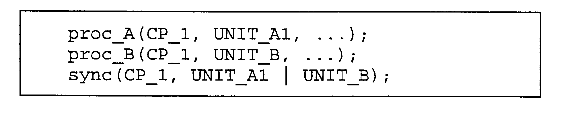
例えば、コプロセッサ11を使って、処理ユニット13Aと処理ユニット13Bの両方が完了してから処理ユニット13Aで処理を行う場合には、以下のようにする。なお、以下の例において、UNIT_A1、UNIT_A2のような添え字は、同じ機能を持つ処理モジュールであることを示している。

ここで、関数proc_Xは、以下のフォーマットを取る。関数名は、処理の種類を表す。cpは使用するコプロセッサ、unitは使用する処理ユニット、wunitは待ちユニットを示す。このほか、使用するメモリやアドレス、画像サイズ、演算のパラメータなども引数で指定する。

sync()を呼ぶと、指定した処理ユニットが空くまで、ファームウェアは待ちに入る。sync()の引数には、使用するコプロセッサcp及び待ちユニットwunitを取る。
前記したように、予め準備した関数だけでは不十分な場合、コプロセッサ11…を構成するFPGA内の論理回路を書き換えることによって、必要な関数を準備することができる。この際には回路設計が必要となってしまうが、コプロセッサ全体ではなく、ユニット単位で変更できるため、回路設計の負担は必要最低限となる。
さらに、FPGAを書き換えた場合でもプロセッサの基本構成は変わらないため、ソフトウェアの互換性を極力保つことができる。例えば、同一機能のユニットは同じ関数名、ユニット名で呼び出せるようにすることで、既存コードの変更を必要最低限にすることができる。
処理ユニット13A…は、処理毎に専用回路で実装されており、演算の同時実行やパイプラインによる並列化がなされている。加えて、並列メモリ121…から複数のデータを同時に読み出すことにより、1クロックに1画素以上の処理を行わせることができる。これらはタスク内での並列処理とみなすことができる。
すなわち、本実施形態においては、並列に動作する複数の画像処理部を用いて、CPUからの指令(つまりプログラム)に従って、タスクレベルでの並列処理を行うことができる。
一方、処理をタスクレベルで並列化するには、以下の方法がある。
1)同一コプロセッサ内で、複数のユニットを同時に使用する。
2)複数のコプロセッサを同時に使う。
1)同一コプロセッサ内で、複数のユニットを同時に使用する。
2)複数のコプロセッサを同時に使う。
同一コプロセッサ内で複数のユニットを同時に使用する場合、複数のユニットが同じメモリへの同時入力、または同時出力を行うことはできない(実行時エラーになる)。これは、FPGAの内部メモリにはアービトレーション機能が無いためである。ただし、メモリにアービトレーション機能が実装されていれば、同時アクセスが可能となる。例えば、並列メモリであるINTRAM1を入力として総和計算をしている間、スケール変換の入力としてINTRAM1を使う事はできないが、他の並列メモリであるINTRAM2を入力とする事は可能である。
また、総和計算のための処理ユニットが二つある場合において、一方の処理ユニットでINTRAM1を入力としている場合、他方の処理ユニットでINTRAM1を入力とする事もできない。
他方、PBSRAM(後述)、フレームメモリなどのように、FPGAの外部にあるメモリに関しては、一般的に、アービトレーション機能が実装されているので、同時にアクセスする事ができる。
アルゴリズムを実装する際に、並列化のために処理を分割する方法としては、
・一枚の画像を分割して、それぞれを別ユニットで実行させる方法、
・テンプレートマッチングなどのように同じ処理を複数回行う場合に、それらを別ユニットで実行させる方法、
・タスクレベルで処理をパイプライン化する方法
などがある。
・一枚の画像を分割して、それぞれを別ユニットで実行させる方法、
・テンプレートマッチングなどのように同じ処理を複数回行う場合に、それらを別ユニットで実行させる方法、
・タスクレベルで処理をパイプライン化する方法
などがある。
一般に同一の処理を複数のユニットに振り分ける場合、リソースの競合の観点から、別々のコプロセッサに割り当てるのがよい。一方、タスク間の依存関係が強い場合は、転送コストを考えると同一コプロセッサ内で割り当てるのがよい。
ここで、本実施形態のように、並列メモリ121…をデュアルポートRAMで構成した場合は、読み込みと書き込みを独立に行うことができる。したがって、処理の出力先が次の処理の入力元になっている場合であっても、後ろの処理が前の処理を追い越さないことが保証できる場合は、処理がすべて完了する前に次の処理を開始できる。
これにより、前の処理が完了し、結果をすべてメモリに書き込むまで次の処理が実行できない場合に比べて、より短いステージでパイプラインを構成することができるため、処理の高速化に貢献できる。つまり、本実施形態では、並列メモリとしてデュアルポート・メモリを用いることによって、CPUの指令(つまりプログラム)に従って、メモリをバッファとしたパイプライン処理を行うことができ、処理を高速化することが可能になる。
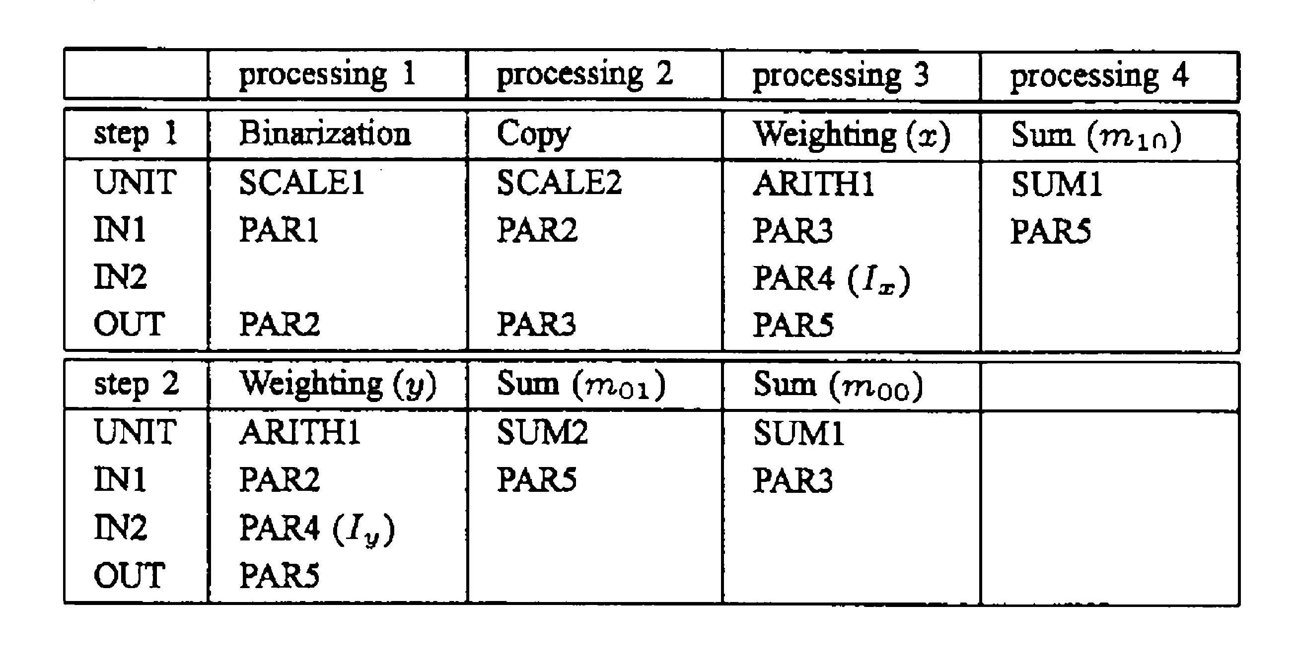
処理のパイプライン化の具体例は後述する(後述の表4)。
(実施例)
上に述べたアーキテクチャに基づいて、本発明者らは、以下に示す評価用のシステムを開発した。システムのデザインと性能評価の結果を示す。
上に述べたアーキテクチャに基づいて、本発明者らは、以下に示す評価用のシステムを開発した。システムのデザインと性能評価の結果を示す。
開発したシステムのブロック図を図3に示す。このシステムは2枚のサブボードが載った1枚のメインボードに実装されている。
メインボードにはFPGA、メモリ、I/Oポートなどが搭載されており、サブボードは、CPUボードとカメラインターフェースボードである。前記した実施形態の要素と実施例のハードウエアとの対応を以下に示す。
・FPGA:コプロセッサ
・DDR2DIMM:フレームメモリ
・DIO、USB、RS-232C、Ethernet(登録商標):I/Oインタフェース
・DDR-SDRAM:メインメモリ
・EXT.BUS:拡張バス。なお、この拡張バスを介して各FPGAはCPUバスに接続されている。したがって、機能上は、この拡張バスは、コプロセッサ間のバスとCPUバスとを兼ねていることになる。
・FPGA:コプロセッサ
・DDR2DIMM:フレームメモリ
・DIO、USB、RS-232C、Ethernet(登録商標):I/Oインタフェース
・DDR-SDRAM:メインメモリ
・EXT.BUS:拡張バス。なお、この拡張バスを介して各FPGAはCPUバスに接続されている。したがって、機能上は、この拡張バスは、コプロセッサ間のバスとCPUバスとを兼ねていることになる。
なお、図3中のPBSRAMは、図1には示していないが、各FPGA用の外部メモリである。
この実施例では、開発コストを抑えるため、CPUボードは市販のCPU基板ESPT-Giga(商品名)を利用し、拡張バスを通じてメインボード内のFPGAと接続している。ESPT-Gigaは、CPUにRenesas SH7763 (SH-4A, 266MHz)、メモリには64MBのDDR-SDRAMを搭載し、入出力として、10/100/1000BASE Ethernet(登録商標)、USB1.1、RS232Cを備えている。
ここで、ESPT-Gigaは、ウェブサーバー機能を内蔵することが可能であり、PCからブラウザを通してシステムを操作したり、処理結果を表示することができる。これにより、LANによる遠隔管理が可能となり、多数のシステムを一台のPCで管理することができるようになっている。
本実施例では、FPGAとして、Altera製のEP2S60F1020C5を2個搭載している。図3中でPBSRAMとあるのは、FPGAのコンフィギュレーションデータを格納するためのフラッシュメモリ(8MBytes)であり、これは、各FPGAに搭載されている。
FPGAはそれぞれフレームメモリ(DRAM)を持っており、カメラからの入力画像は自動的にFPGA1のフレームメモリに溜められる。カメラインタフェースはFPGA1に接続されている。個別のカメラ用の物理インタフェースは、メインボード上に取り付けられるカメラインタフェース基板に実装されて使用される。本実施例の実装では、カメラ用のインタフェースは、Basler製のA504k(モノクロ)/kc(カラー)と、Microtron製のEosens MC1362(モノクロ)/1363(カラー)に対応している。これらのカメラは、最大で1280×1024画素の画像を、500fpsでリアルタイム出力することができる。また、これらのカメラでは、画像の行数を減らすことでフレームレートを上げることが可能となっており、たとえば1280×512画素であれば1000fpsで出力できる。
前記したA504k/kcおよびMC1362/1363は、Camera Link規格を独自拡張したインタフェースを採用しており、2本のCamera Link ケーブルでボードと接続される。これらのカメラは、通常のCamera Linkインタフェースのカメラと、物理層での互換性があるので、FPGA1の回路を変更することにより、他のカメラにも対応できる。さらに、本実施例では、カメラインタフェース基板を交換することで、IEEE1394やGigabit Ethernet(登録商標)などの他のカメラインターフェースにも対応できるようになっている。
また、FPGA1には、アナログVGAポートが接続されており、フレームメモリに蓄えられた画像をSXGAサイズ(1280×1024)でディスプレイに出力できるようになっている。
なお、本実施例の画像処理装置では、フレームメモリとは別に、各FPGAが、小容量のSRAMを持っている。本実施例では、このSRAMを、後述の座標変換処理における入力元として利用できる。
さらに、本実施例では、ESPT-Gigaでの外部入出力機能とは別に、32ビットのデジタルI/O(DIO)を用意しており、ロボット制御など高いリアルタイム性が要求される用途に利用できる。
本実施例における各モジュール間での動作速度は以下の通りである。
・FPGA-DRAM間:3200MB/s (200MHz, 128bit);
・FPGA-SRAM間:1333MB/s (166.6MHz, 64bit);
・FPGA-CPU間:133MB/s (66.67MHz, 16bit);
・FPGA-FPGA間:2133MB/s (133.33MHz, 128bit)。
・FPGA-DRAM間:3200MB/s (200MHz, 128bit);
・FPGA-SRAM間:1333MB/s (166.6MHz, 64bit);
・FPGA-CPU間:133MB/s (66.67MHz, 16bit);
・FPGA-FPGA間:2133MB/s (133.33MHz, 128bit)。
以上述べた本実施例のボードのスペックを下記表1にまとめた。

本実施例では、二つのFPGAのそれぞれに、前記の実施形態で説明したコプロセッサが実装されている。各コプロセッサは、以下のユニットを持つ。
・二つの並列メモリ(64kbytes) (PAR1, PAR4);
・四つの並列メモリ(16kbytes) (PAR2, PAR3, PAR5, PAR6);
・二つのDMA制御ユニット(DMA1, DMA2);
・九つの処理ユニット(後述の表2及び表3参照);
・命令ディスクリプタ。
・二つの並列メモリ(64kbytes) (PAR1, PAR4);
・四つの並列メモリ(16kbytes) (PAR2, PAR3, PAR5, PAR6);
・二つのDMA制御ユニット(DMA1, DMA2);
・九つの処理ユニット(後述の表2及び表3参照);
・命令ディスクリプタ。
本実施例のコプロセッサでは、1画素を16bitとして処理する。カメラから送られてくる画像は一般に8bitであることが多いが、演算の途中過程において、それ以上の精度が必要になることもあるため、16bitを標準とした。たとえば8bit画像同士を加算あるいは減算した場合の結果は9bitである。フィルタ処理など多くの画素を重み付きで足し合わせる場合には、それ以上のビット数が必要となる。
カラー画像の処理は、RGBそれぞれを3枚の独立したグレースケール画像として扱う。画像の処理ユニットで計算を行う時、16bitの入力データの扱いと出力データの扱いをそれぞれ以下のように指定する事ができる。
・入力データを、
1)0x0000~0xffffとして解釈(符号無し);
2)-0x8000~0x7fffとして解釈(符号付き)。
・演算結果を、
1)0x0000~0xffffで表現;
2)-0x8000~0x7fffで表現;
3)絶対値をとって、0x0000~0xffffで表現。
・演算結果が16bitに収まらない場合は最大値か最小値のいずれかで飽和させる。
・二値化を行う場合、結果yがTl≦y≦Thの場合は1、それ以外は0とする。ここで、Tl及びThは、適宜に設定される閾値の上限及び下限を示す。
・入力データを、
1)0x0000~0xffffとして解釈(符号無し);
2)-0x8000~0x7fffとして解釈(符号付き)。
・演算結果を、
1)0x0000~0xffffで表現;
2)-0x8000~0x7fffで表現;
3)絶対値をとって、0x0000~0xffffで表現。
・演算結果が16bitに収まらない場合は最大値か最小値のいずれかで飽和させる。
・二値化を行う場合、結果yがTl≦y≦Thの場合は1、それ以外は0とする。ここで、Tl及びThは、適宜に設定される閾値の上限及び下限を示す。
画像処理の係数パラメータは、16bit長または12bit長の符号付固定小数点とし、小数点の位置は各パラメータ共通で指定する。
並列メモリは、一つにつき同時に128bit(8pixel)のデータの読み書きができる。また、この並列メモリは、デュアルポートRAMで構成されており、読み込みと書き込みを独立に行うことができる。
DMA制御ユニット(DMAC)は、各メモリ間のデータの転送を行う。本実施例では、CPUとのデータ転送は、各FPGAにおいて、特定のDMAC(例えばDMA2とする)でのみ可能である。また、他方のFPGAにデータを転送できるのは、各FPGAにおいて、他の特定のDMAC(例えばDMA1とする)のみである。各メモリ間でのデータ転送は、128bit単位で行われるが、外部メモリとの間でデータ転送をするときは、外部メモリの動作速度に制限される。
データの転送範囲としては、
・(一行あたり転送バイト数)×(行数)の設定;
・ソース及びディスティネーションそれぞれの転送開始アドレスと一行あたりのアドレス増分
を指定する。これによって大画面の画像の一部切り出し、埋め込みが可能である。
・(一行あたり転送バイト数)×(行数)の設定;
・ソース及びディスティネーションそれぞれの転送開始アドレスと一行あたりのアドレス増分
を指定する。これによって大画面の画像の一部切り出し、埋め込みが可能である。
本実施例のDMA制御ユニット(DMAC)には、オプションで以下のデータ操作回路(すなわち画像処理機能)を備えることができる。
シフト回路
この回路は、16バイト毎にデータを左にバイト単位でシフトした結果を出力するものである。データのsrcアドレスについては、16の倍数でなければならないという制限があるが、シフト回路を使うと、任意のアドレスのデータをsrcとすることができる。
この回路は、16バイト毎にデータを左にバイト単位でシフトした結果を出力するものである。データのsrcアドレスについては、16の倍数でなければならないという制限があるが、シフト回路を使うと、任意のアドレスのデータをsrcとすることができる。
間引き回路
この回路は、16バイト毎にデータ入力を受け付け、8→1(出力データ量1/8倍), 4→1(出力データ量1/4倍), 2→1(出力データ量1/2倍)のいずれかの間引きを行ったデータを出力する。この機能とDMA転送のアドレス増分の指定とにより、画像の縮小を行うことができる。
この回路は、16バイト毎にデータ入力を受け付け、8→1(出力データ量1/8倍), 4→1(出力データ量1/4倍), 2→1(出力データ量1/2倍)のいずれかの間引きを行ったデータを出力する。この機能とDMA転送のアドレス増分の指定とにより、画像の縮小を行うことができる。
変換回路
この回路では、16バイト毎にデータを入力する。そして、8ビット(モノクロ)→16ビット(出力データ量は2倍)、8ビット(ベイヤー)→16ビット(R成分、G成分、B成分のいずれか)、16ビット→8ビット(出力データ量は1/2倍)のいずれかの変換を行うことができる。カメラから送られてくるデータは1画素が8ビットで構成されており、これをコプロセッサで処理するためには、1画素16ビットに変換する必要がある。カラーカメラの場合、ベイヤー変換を行い、RGBのいずれかの成分のみを出力する処理を行う。
この回路では、16バイト毎にデータを入力する。そして、8ビット(モノクロ)→16ビット(出力データ量は2倍)、8ビット(ベイヤー)→16ビット(R成分、G成分、B成分のいずれか)、16ビット→8ビット(出力データ量は1/2倍)のいずれかの変換を行うことができる。カメラから送られてくるデータは1画素が8ビットで構成されており、これをコプロセッサで処理するためには、1画素16ビットに変換する必要がある。カラーカメラの場合、ベイヤー変換を行い、RGBのいずれかの成分のみを出力する処理を行う。
表2に、各コプロセッサに実装されている演算ユニット(すなわち処理ユニット)を示す。
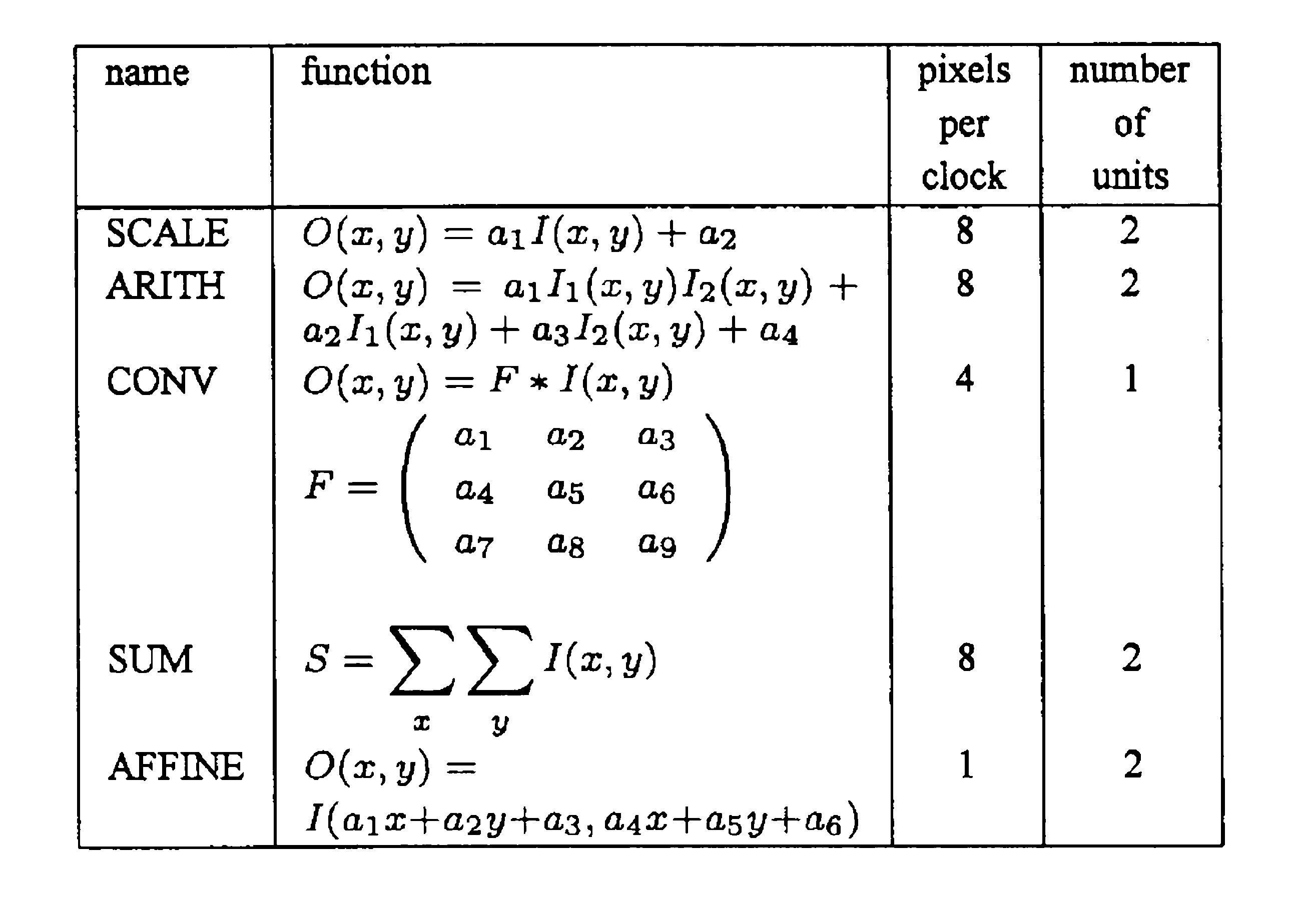
この表における記号の意味は以下の通りである・
・SCALE:画素値を線形にスケーリングする処理;
・ARITH:二つの画像間で加減算、乗算を行う処理;
・3x3CONV:オペレータのカーネルサイズが3×3のコンボリューションフィルタ;
・SUM:指定した範囲で画素値の総和を計算する処理;
・AFFINE:画像を平面アフィン変換で変形する処理。
・SCALE:画素値を線形にスケーリングする処理;
・ARITH:二つの画像間で加減算、乗算を行う処理;
・3x3CONV:オペレータのカーネルサイズが3×3のコンボリューションフィルタ;
・SUM:指定した範囲で画素値の総和を計算する処理;
・AFFINE:画像を平面アフィン変換で変形する処理。
ここで、AFFINEは、入力をSRAMから受け取ることができる。SCALE、ARITH、SUMは、1クロックに8画素、3x3CONVは1クロックに4画素、同時に処理を行うことができる。AFFINEは1クロックに1画素だけ処理を行う。
本実施例では、画像処理のための処理ユニットとして、一般的によく用いられる画像処理アルゴリズムを実現するのに必要最低限と思われる基本機能を搭載した。他に、処理ユニットに実装することが有用な機能としては、「ルックアップ・テーブル(LUT)を用いた非線形のスケール変換」、「ルックアップ・テーブル(LUT)を用いた非線形の座標変換」及び「論理演算」などが挙げられる。
本実施例のディスクリプタは、それぞれ256Word(1Word=2bytes)まで命令を積むことができる。一つの命令は、パラメータの数により1~3Wordで構成される。ここで、一つの命令は、前記したproc_X()関数の一つに対応し、一つのDMA制御ユニットまたは画像処理ユニットを用いて、指定した範囲の画像データに対する処理を指示することができる。なお、何もしないという命令も用意されており、これはsync()関数に対応する。
(動作周波数、回路規模などのスペック)
本実施例で用いたFPGAは、200MHzで動作し、使用リソースはFPGA1が88%、FPGA2が81%である。
本実施例で用いたFPGAは、200MHzで動作し、使用リソースはFPGA1が88%、FPGA2が81%である。
表3に、本実施例のシステムが持つ基本機能を用いた処理と、基本機能を組み合わせた処理の計算時間を示す。比較のため、OpenCVを用いて同等の処理をPCに実装した場合の計算時間も示す。使用したPCは、CPUがIntel E6300 (1.86GHz×2)、RAMが3GBで、Visual Studio 2005とOpenCV 1.0を用いて実装し、Windows(登録商標) XP上で計測した。表中のEvalSysは、開発した評価システムを用いた場合の処理時間、OpenCVはPCとOpenCVを用いた場合の処理時間を示す。
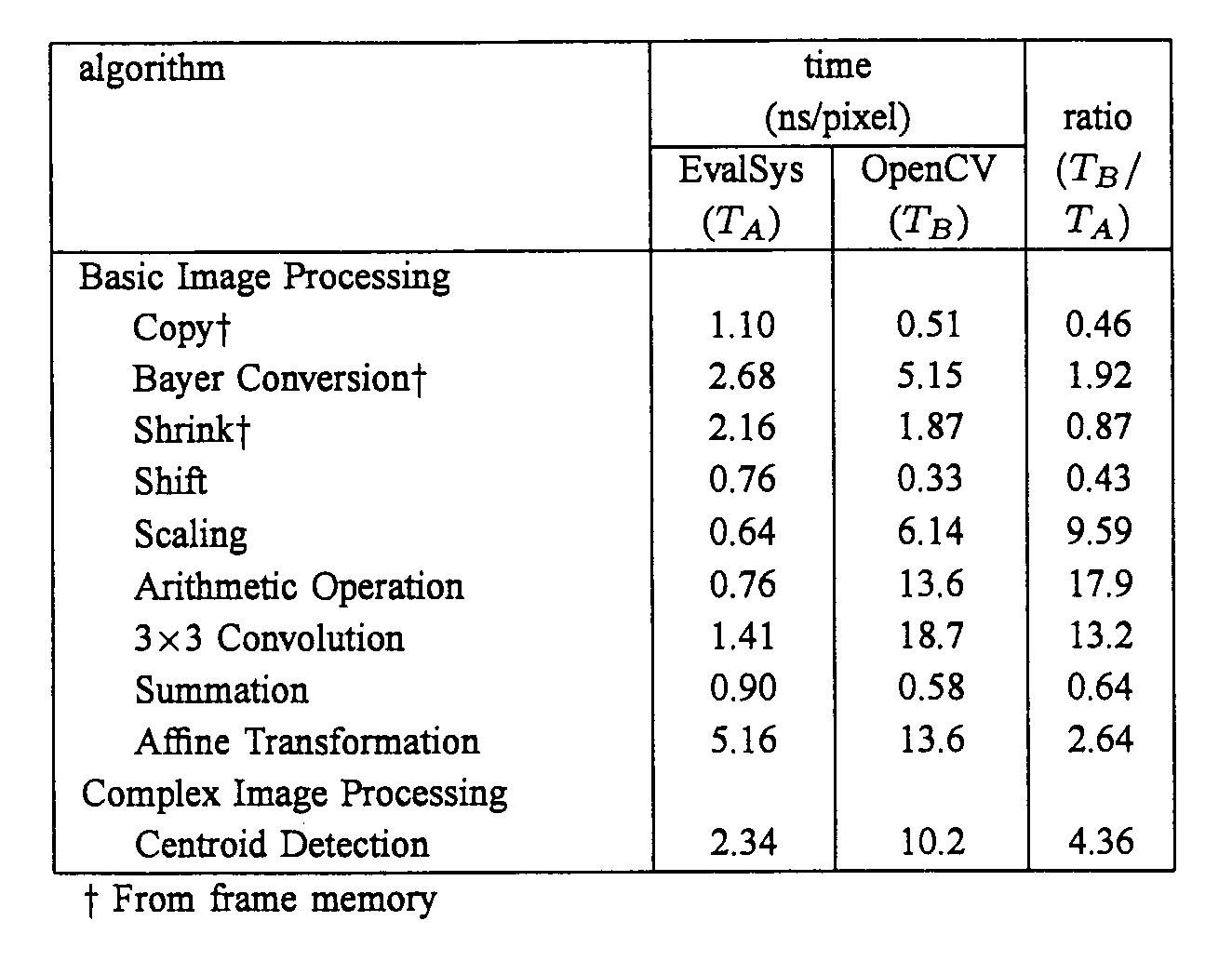
本実施例において、入力元・出力先はFPGA内部の並列メモリとし、画像の大きさは256×32とした。
一方、PCでの計測は、同じ処理を100000回繰り返し行い、実行時間の平均を用いた。実装はOpenCVのライブラリを用いて行い、画像は符号付き16ビットとした。ただし、ベイヤー変換およびアフィン変換については、OpenCVの関数が符号付き16ビットに対応していなかったので、符号なし8ビットで実装した。係数は、関数の仕様に合わせてfloatまたはdoubleを用いた。Copy、Bayer Conversion、Shrinkの三つの関数については、カメラから取り込まれた画像に対して最初に行うことが想定されるため、入力元をフレームメモリとし、PCでの計測は直前の処理におけるキャッシュの影響を排除するようにした。また、Bayer ConversionとShrinkは入力と出力で画像サイズが異なるが、出力の画像サイズを基準に算出した。
重心計算は、まず入力画像から前フレームの結果から推定される対象が存在する領域を切り出し、固定あるいは適応的に定められたしきい値で二値化する。次に、以下の式を用いて重心の計算を行う。
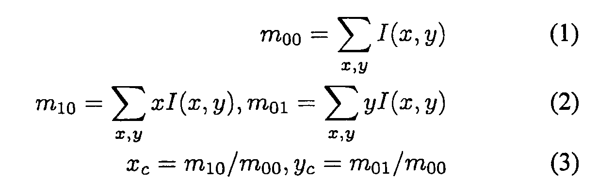
(x,y)座標値での重みIx及びIyはそれぞれあらかじめ並列メモリに入れておき、二値化した入力画像をARITHにより重み付けし、SUMによる総和計算でモーメントm10及びm01を計算する。モーメントm00は重み付けなしで総和計算により求める。
これらの処理は、表4に示すような形で、タスクレベルでパイプライン化し、並列に実行する。並列メモリはデュアルポートになっているため、処理の出力先が次の処理の入力元になっている場合、処理がすべて完了する前に次の処理を開始できる。なお、本実施例における前記の処理はすべてコプロセッサ1のみで行った。
これらの結果から、本実施例によれば、平均的にはPCを数倍上回る性能が得られていることがわかった。しかし、今回PCと比較したのは、他の一般的な手法と比較する際の基準となるからであり、PCベースのシステムを用いない理由は、安定性や信頼性を確保するためである。実際、PCを用いたシステムではディレイやフレーム落ちが頻繁に観測されており、高速ビジョンのアプリケーションにおいて支障をきたすことになる。
また、PCを用いた場合でも、マルチメディア命令やGPUの利用により高速化が可能であり、この場合、開発したシステムより高い演算性能を実現することができる。たとえば、GPUを用いた枠組みの一つであるGPUCV(非特許文献30)では、いくつかの画像処理においてPCの1.7~18倍の処理性能が報告されている。しかし、これらはPCのプラットフォームを前提にしており、やはり上記の問題を抱えることになる。
開発したボードは12V,5Aの電源で動作し、実効的な消費電力は42W程度であった。FPGAの消費電力は比較的高いため、DSPなどを利用する場合に比べると消費電力は高くなるが、本実施形態では、組込みシステムを用いることにより、安定性と信頼性を確保できるという利点がある。
本実施例では、高速ビジョンシステムのアーキテクチャとして、組み込みマイクロプロセッサとFPGAを組み合わせることによって、ハードウェアのリコンフィギャラビリティとアルゴリズム実装の容易性を両立できるという利点がある。
半導体の集積化が指数的に進む中、並列処理を活かしたプロセッシングアーキテクチャは今後よりいっそう重要になってくる。その際に、汎用的なアーキテクチャでは、並列度を最大限に活かすことは難しい。FPGAによる再構成可能な専用回路と、CPUの容易なプログラミング環境を組み合わせることで、高い画像処理性能を発揮しつつ、ある程度の汎用性を持たせることができる。
再構成可能なプログラマブル・ロジック・デバイスは、通常、FPGAと呼ばれる集積回路である。FPGAを用いることにより、画像処理部の機能を、ユーザの必要に応じて書き換えることができる。例えば、不足する関数に対応する画像処理部を追加したり、あるいは、必要な関数に対応する画像処理部を追加することができる。
本実施例では、並列メモリとしてデュアルポート・メモリを用いることにより、メモリへの読み込みと書き込みとを独立に行うことができる。このため、処理を一層高速化することができる。
また、ディスクリプタを用いることにより、CPUは、コプロセッサに対して、一度に複数の処理を指示することができる。このため、コプロセッサの動作完了時におけるCPUへの割り込み回数を減らすことができるという利点がある。
画像処理部は、画像処理に用いられる特定の関数に対応する。画像処理を行う場合、処理に必要な関数の実行を、専用の画像処理部で行うことにより、処理を高速化できる。さらに、プログラムにおいては、特定の関数あるいは画像処理部を指定して処理を実行させることができる。
なお、前記した実施形態及び実施例の構成は、本発明の例示に過ぎず、本発明の内容を制限する趣旨のものではない。
Claims (11)
- コプロセッサと、フレームメモリと、CPUとを備えており、
前記フレームメモリは、処理されるべき画像データを格納する構成となっており、
前記コプロセッサは、複数の画像処理部と複数の並列メモリとを備えており、
前記並列メモリは、前記フレームメモリに格納された前記画像データの全部又は一部を受け取って前記画像処理部のいずれかに送る構成となっており、
前記複数の画像処理部は、いずれも、画像処理のための関数に対応した機能を有しており、
かつ、前記複数の画像処理部は、前記CPUからの指令に従って、
前記並列メモリ又は前記フレームメモリから、前記画像データの全部又は一部を受け取り、さらに、
前記画像データの全部又は一部に対して、前記画像処理のための関数に従った処理を行う構成となっている
画像処理装置。 - 前記コプロセッサは、再構成可能なプログラマブル・ロジック・デバイスによって構成されている
請求項1に記載の画像処理装置。 - 前記複数の並列メモリは、デュアルポート・メモリである
請求項1又は2に記載の画像処理装置。 - 前記画像処理部は、ダイレクト・メモリ・アクセス・コントローラと、処理ユニットとを備えており、
前記ダイレクト・メモリ・アクセス・コントローラは、前記並列メモリの動作を制御する構成となっており、
前記処理ユニットは、前記画像処理のための関数に従った処理を行う構成となっている
請求項1~3のいずれか1項に記載の画像処理装置。 - 前記コプロセッサを複数個備えている
請求項1~4のいずれか1項に記載の画像処理装置。 - 前記複数のコプロセッサは、共通のコプロセッサ・バスに接続されている
請求項5に記載の画像処理装置。 - 前記コプロセッサは、ディスクリプタをさらに備えており、
前記CPUは、前記コプロセッサへの命令を前記ディスクリプタに書き込む構成となっており、
前記コプロセッサは、前記ディスクリプタに書かれている命令を読み取り、前記複数の画像処理部による処理を実行する構成となっている
請求項1~6のいずれか1項に記載の画像処理装置。 - 前記複数の画像処理部は、前記CPUからの指令に従って、独立して並列に動作する構成となっている
請求項1~7のいずれか1項に記載の画像処理装置。 - 以下のステップを備える画像処理方法:
(1)フレームメモリが、処理されるべき画像データを格納するステップ;
(2)並列メモリが、前記フレームメモリに格納された前記画像データの全部又は一部を受け取るステップ;
(3)前記複数の画像処理部が、CPUからの指令に従って、前記並列メモリ又は前記フレームメモリから、前記画像データの全部又は一部を受け取るステップ;
(4)前記複数の画像処理部が、前記CPUからの指令に従って、前記画像データの全部又は一部に対して、画像処理のための関数に従った処理をそれぞれ行うステップ。 - 前記並列メモリとして、デュアルポート・メモリが用いられており、
さらに、複数の画像処理部は、前記CPUからの指令に従って、前記並列メモリをバッファとしたパイプライン処理を行うものである
請求項9に記載の画像処理方法。 - 前記複数の画像処理部は、前記CPUからの指令に従って、独立して並列に動作する構成となっており、
さらに、前記複数の画像処理部は、前記CPUからの指令に従って、タスクレベルでの並列処理を行うものである
請求項9又は10に記載の画像処理方法。
Priority Applications (3)
| Application Number | Priority Date | Filing Date | Title |
|---|---|---|---|
| US13/392,510 US20120147016A1 (en) | 2009-08-26 | 2010-08-13 | Image processing device and image processing method |
| CN201080037961XA CN102483842A (zh) | 2009-08-26 | 2010-08-13 | 图像处理装置和图像处理方法 |
| EP10811704.5A EP2472468A4 (en) | 2009-08-26 | 2010-08-13 | IMAGE PROCESSING DEVICE AND IMAGE PROCESSING METHOD |
Applications Claiming Priority (2)
| Application Number | Priority Date | Filing Date | Title |
|---|---|---|---|
| JP2009-195777 | 2009-08-26 | ||
| JP2009195777A JP2011048579A (ja) | 2009-08-26 | 2009-08-26 | 画像処理装置及び画像処理方法 |
Publications (1)
| Publication Number | Publication Date |
|---|---|
| WO2011024654A1 true WO2011024654A1 (ja) | 2011-03-03 |
Family
ID=43627760
Family Applications (1)
| Application Number | Title | Priority Date | Filing Date |
|---|---|---|---|
| PCT/JP2010/063740 Ceased WO2011024654A1 (ja) | 2009-08-26 | 2010-08-13 | 画像処理装置及び画像処理方法 |
Country Status (5)
| Country | Link |
|---|---|
| US (1) | US20120147016A1 (ja) |
| EP (1) | EP2472468A4 (ja) |
| JP (1) | JP2011048579A (ja) |
| CN (1) | CN102483842A (ja) |
| WO (1) | WO2011024654A1 (ja) |
Cited By (2)
| Publication number | Priority date | Publication date | Assignee | Title |
|---|---|---|---|---|
| CN102446342A (zh) * | 2011-08-30 | 2012-05-09 | 西安交通大学 | 可重构二值运算器、可重构二值图像处理系统及其实现基本形态学算法的方法 |
| CN104200467A (zh) * | 2014-08-25 | 2014-12-10 | 西安交通大学 | 可重构灰度形态学图像处理器及其灰度运算单元和实现形态学运算的方法 |
Families Citing this family (19)
| Publication number | Priority date | Publication date | Assignee | Title |
|---|---|---|---|---|
| US8803897B2 (en) * | 2009-09-03 | 2014-08-12 | Advanced Micro Devices, Inc. | Internal, processing-unit memory for general-purpose use |
| JP5653865B2 (ja) * | 2011-08-23 | 2015-01-14 | 日本電信電話株式会社 | データ処理システム |
| JP5876319B2 (ja) * | 2012-02-21 | 2016-03-02 | 日本電信電話株式会社 | サービス提供システム、サービス提供方法、リソースマネージャ、プログラム |
| US9098917B2 (en) * | 2012-07-19 | 2015-08-04 | Samsung Electronics Co., Ltd. | Method and system for accelerating collision resolution on a reconfigurable processor |
| CN103018515B (zh) * | 2012-12-12 | 2014-09-24 | 电子科技大学 | 一种具有无缝测量能力的数字示波器 |
| CN103020972A (zh) * | 2012-12-28 | 2013-04-03 | 中国科学院长春光学精密机械与物理研究所 | 一种基于嵌入式处理器的二值图像连通域检测方法 |
| JP6176162B2 (ja) | 2014-03-19 | 2017-08-09 | 株式会社デンソー | データ処理装置 |
| CN105895030B (zh) * | 2014-12-15 | 2019-08-09 | 恩智浦美国有限公司 | 用于持久性显示面板的控制器 |
| CN108430313B (zh) * | 2016-01-04 | 2021-08-17 | 深圳迈瑞生物医疗电子股份有限公司 | 医疗设备间协同控制系统和方法及医疗工作站和通讯设备 |
| CN108885776B (zh) * | 2016-03-24 | 2022-09-27 | 富士胶片株式会社 | 图像处理装置、图像处理方法及存储介质 |
| CN107766021B (zh) * | 2017-09-27 | 2020-12-25 | 芯启源(上海)半导体科技有限公司 | 图像处理方法、设备、显示系统及存储介质 |
| CN107992100B (zh) * | 2017-12-13 | 2021-01-15 | 中国科学院长春光学精密机械与物理研究所 | 基于可编程逻辑阵列的高帧频图像跟踪方法和系统 |
| CN111833232B (zh) * | 2019-04-18 | 2024-07-02 | 杭州海康威视数字技术股份有限公司 | 一种图像处理装置 |
| CN110189244A (zh) * | 2019-06-06 | 2019-08-30 | 卡瓦科尔牙科医疗器械(苏州)有限公司 | 用于ct影像设备的加速图像处理系统 |
| CN111064906A (zh) * | 2019-11-27 | 2020-04-24 | 北京计算机技术及应用研究所 | 国产处理器和国产fpga多路4k高清视频综合显示方法 |
| CN112001836A (zh) * | 2020-07-03 | 2020-11-27 | 北京博雅慧视智能技术研究院有限公司 | 一种图像处理装置 |
| US20230100586A1 (en) * | 2021-09-24 | 2023-03-30 | Intel Corporation | Circuitry and methods for accelerating streaming data-transformation operations |
| CN116112677B (zh) * | 2022-12-27 | 2025-09-09 | 浙江大立科技股份有限公司 | 基于FPGA仿射逆变换的bayer图像解码方法 |
| US20250005704A1 (en) * | 2023-06-28 | 2025-01-02 | Texas Instruments Incorporated | Methods and apparatus to animate a splash screen |
Citations (3)
| Publication number | Priority date | Publication date | Assignee | Title |
|---|---|---|---|---|
| JPH0573516A (ja) * | 1991-09-12 | 1993-03-26 | Sony Corp | 信号処理用プロセツサ |
| JPH06131155A (ja) * | 1991-01-29 | 1994-05-13 | Analogic Corp | 再構成可能な順次処理装置 |
| JPH1185963A (ja) * | 1997-04-30 | 1999-03-30 | Canon Inf Syst Res Australia Pty Ltd | 画像処理装置及びその方法 |
Family Cites Families (27)
| Publication number | Priority date | Publication date | Assignee | Title |
|---|---|---|---|---|
| JPS6057457A (ja) * | 1983-09-07 | 1985-04-03 | Ricoh Co Ltd | Dma装置 |
| US5584032A (en) * | 1984-10-17 | 1996-12-10 | Hyatt; Gilbert P. | Kernel processor system |
| US5121480A (en) * | 1988-07-18 | 1992-06-09 | Western Digital Corporation | Data recording system buffer management and multiple host interface control |
| US5392391A (en) * | 1991-10-18 | 1995-02-21 | Lsi Logic Corporation | High performance graphics applications controller |
| US5808690A (en) * | 1996-01-02 | 1998-09-15 | Integrated Device Technology, Inc. | Image generation system, methods and computer program products using distributed processing |
| JP3727711B2 (ja) * | 1996-04-10 | 2005-12-14 | 富士通株式会社 | 画像情報処理装置 |
| US6567564B1 (en) * | 1996-04-17 | 2003-05-20 | Sarnoff Corporation | Pipelined pyramid processor for image processing systems |
| US6061749A (en) * | 1997-04-30 | 2000-05-09 | Canon Kabushiki Kaisha | Transformation of a first dataword received from a FIFO into an input register and subsequent dataword from the FIFO into a normalized output dataword |
| US5923893A (en) * | 1997-09-05 | 1999-07-13 | Motorola, Inc. | Method and apparatus for interfacing a processor to a coprocessor |
| US7446774B1 (en) * | 1998-11-09 | 2008-11-04 | Broadcom Corporation | Video and graphics system with an integrated system bridge controller |
| JP2002142149A (ja) * | 2000-11-06 | 2002-05-17 | Mega Chips Corp | 画像処理回路 |
| US6657621B2 (en) * | 2001-05-01 | 2003-12-02 | Hewlett-Packard Development Company, L.P. | Device and method for scrolling stored images across a display |
| EP1296288B1 (en) * | 2001-09-21 | 2006-04-19 | Interuniversitair Microelektronica Centrum Vzw | A 2D FIFO device and method for use in block based coding applications |
| US7577822B2 (en) * | 2001-12-14 | 2009-08-18 | Pact Xpp Technologies Ag | Parallel task operation in processor and reconfigurable coprocessor configured based on information in link list including termination information for synchronization |
| US20030135535A1 (en) * | 2002-01-11 | 2003-07-17 | Hoeflinger Jay P. | Transferring data between threads in a multiprocessing computer system |
| US7489834B2 (en) * | 2003-01-17 | 2009-02-10 | Parimics, Inc. | Method and apparatus for image processing |
| US7015915B1 (en) * | 2003-08-12 | 2006-03-21 | Nvidia Corporation | Programming multiple chips from a command buffer |
| KR20070083546A (ko) * | 2004-08-31 | 2007-08-24 | 실리콘 옵틱스 인코포레이션 | 비트 판 리소스의 관리를 위한 방법 및 장치 |
| TWI322354B (en) * | 2005-10-18 | 2010-03-21 | Via Tech Inc | Method and system for deferred command issuing in a computer system |
| WO2007114059A1 (ja) * | 2006-04-05 | 2007-10-11 | Nec Corporation | データ処理装置 |
| US20080055326A1 (en) * | 2006-09-05 | 2008-03-06 | Yun Du | Processing of Command Sub-Lists by Multiple Graphics Processing Units |
| US7950003B1 (en) * | 2006-12-07 | 2011-05-24 | Sony Computer Entertainment Inc. | Heads-up-display software development tool for analyzing and optimizing computer software |
| JP4889573B2 (ja) * | 2007-06-07 | 2012-03-07 | ヤマハ株式会社 | 画像処理装置 |
| JP4933361B2 (ja) * | 2007-06-26 | 2012-05-16 | 日本電波工業株式会社 | マッチドフィルタ |
| JP5262578B2 (ja) * | 2008-10-27 | 2013-08-14 | 富士ゼロックス株式会社 | 電子機器 |
| US8310482B1 (en) * | 2008-12-01 | 2012-11-13 | Nvidia Corporation | Distributed calculation of plane equations |
| US8310488B2 (en) * | 2009-04-02 | 2012-11-13 | Sony Computer Intertainment America, Inc. | Dynamic context switching between architecturally distinct graphics processors |
-
2009
- 2009-08-26 JP JP2009195777A patent/JP2011048579A/ja active Pending
-
2010
- 2010-08-13 US US13/392,510 patent/US20120147016A1/en not_active Abandoned
- 2010-08-13 EP EP10811704.5A patent/EP2472468A4/en not_active Withdrawn
- 2010-08-13 WO PCT/JP2010/063740 patent/WO2011024654A1/ja not_active Ceased
- 2010-08-13 CN CN201080037961XA patent/CN102483842A/zh active Pending
Patent Citations (3)
| Publication number | Priority date | Publication date | Assignee | Title |
|---|---|---|---|---|
| JPH06131155A (ja) * | 1991-01-29 | 1994-05-13 | Analogic Corp | 再構成可能な順次処理装置 |
| JPH0573516A (ja) * | 1991-09-12 | 1993-03-26 | Sony Corp | 信号処理用プロセツサ |
| JPH1185963A (ja) * | 1997-04-30 | 1999-03-30 | Canon Inf Syst Res Australia Pty Ltd | 画像処理装置及びその方法 |
Non-Patent Citations (30)
| Title |
|---|
| A. NAMIKI; Y. NAKABO; I. ISHII; M. ISHIKAWA: "1 ms sensory-motor fusion system", IEEE TRANSACTIONS ON MECHATORONICS, vol. 5, no. 3, 2000, pages 244 - 252, XP011034293 |
| B. KHAILANY; T. WILLIAMS; J. LIN; E. LONG; M. RYGH; D. TOVEY; W. DALLY: "A programmable 512 GOPS stream processor for signal, image, and video processing", IEEE JOURNAL OF SOLID-STATE CIRCUITS, vol. 43, 2008, pages 202 - 213 |
| H. NODA; M. NAKAJIMA; K. DOSAKA; K. NAKATA; M. HIGASHIDA; O. YAMAMOTO; K. MIZUMOTO; T. TANIZAKI; T. GYOHTEN; Y. OKUNO: "The design and implementation of the massively parallel processor based on the matrix architecture", PROC. IEEE JOURNAL OF SOLID-STATE CIRCUITS, vol. 42, no. 1, 2007, pages 183 - 192, XP011152712, DOI: doi:10.1109/JSSC.2006.886545 |
| H. OKU; N. OGAWA; K. HASHIMOTO; M. ISHIKAWA: "Two- dimensional tracking of a motile microorganism allowing high-resolution observation with various imaging techniques", REVIEW OF SCIENTIFIC INSTRUMENTS, vol. 76, no. 3, 2005, pages 034301, XP012079269, DOI: doi:10.1063/1.1857632 |
| I. ISHII; K. YAMAMOTO; K. DOI; T. TSUJI: "High-speed 3D image acquisition using coded structured light projection", PROC. IEEE/RSJ INTERNATIONAL CONFERENCE ON INTELLIGENT ROBOTS AND SYSTEMS, 2007, pages 925 - 930 |
| I. ISHII; Y. NIE; K. YAMAMOTO; K. ORITO; H. MATSUDA: "Real-time and long-time quantification of behavior of laboratory mice scratching", PROC. IEEE INTERNATIONAL CONFERENCE ON AUTOMATION SCIENCE AND ENGINEERING, 2007, pages 628 - 633, XP031141531 |
| IEEE JOURNAL OF SOLID-STATE CIRCUITS, vol. 43, no. 1, 2008, pages 192 - 201 |
| J. EKLUND; C. SVENSSON; A. A°STRO''M: "VLSI implementation of a focal plane image processor-a realization of the near-sensor image processing concept", IEEE TRANSACTIONS ON VERY LARGE SCALE INTEGRAT. (VLSI) SYSTEMS, vol. 4, no. 3, 1996, pages 322 - 335, XP011326063, DOI: doi:10.1109/92.532033 |
| J. FARRUGIA; P. HORAIN; E. GUEHENNEUX; Y. ALUSSE: "GPUCV: a framework for image processing acceleration with graphics processors", PROC. IEEE INTERNATIONAL CONFERENCE ON MULTIMEDIA AND EXPO, 2006, pages 585 - 588, XP031032903 |
| J. TANABE; Y. TANIGUCHI; T. MIYAMORI; Y. MIYAMOTO; H. TAKEDA; M. TARUI; H. NAKAYAMA; N. TAKEDA; K. MAEDA; M. MATSUI: "Visconti: multi VLIW image recognition processor based on configurable processor", PROC. IEEE CUSTOM INTEGRATED CIRCUITS CONFERENCE, 2003, pages 185 - 188, XP010671202, DOI: doi:10.1109/CICC.2003.1249398 |
| K. SHIMIZU; S.HIRAI: "CMOS + FPGA vision system for visual feed back of mechanical systems", PROC. IEEE INTERNATIONAL CONFERENCE ON ROBOTICS AND AUTOMATION, 2006, pages 2060 - 2065 |
| K. YAMANE; T. KURODA; Y. NAKAMURA: "High-precision and high-speed motion capture combining heterogeneous cameras", PROC. IEEE/RSJ INTERNATIONAL CONFERENCE ON INTELLIGENT ROBOTS AND SYSTEMS, 2004, pages 279 - 286, XP010765548, DOI: doi:10.1109/IROS.2004.1389365 |
| M. WIRTHLIN; B. HUTCHINGS; K. GILSON: "The nanoprocessor: a low resource reconfigurable processor", PROC. IEEE WORKSHOP ON FPGAS FOR CUSTOM COMPUTING MACHINES, 1994, pages 23 - 30 |
| N. FURUKAWA; A. NAMIKI; T. SENOO; M. ISHIKAWA: "Dynamic regrasping using a high-speed multi-fingered hand and a high-speed vision system", PROC. IEEE INTERNATIONAL CONFERENCE ON ROBOTICS AND AUTOMATION, 2006, pages 181 - 187 |
| P. DUDEK; P. HICKS: "A general-purpose processor-per-pixel analog SIMD vision chip", IEEE TRANSACTIONS ON CIRCUITS AND SYSTEMS I: REGULAR PAPERS, vol. 52, no. 1, 2005, pages 13 - 20 |
| PROC. IEEE TECHNICAL EXHIBITION BASED CONFERENCE ON ROBOTICS AND AUTOMATION, 2004, pages 9 - 10 |
| R. GINHOUX; J. GANGLOFF; M. DE MATHELIN; L. SOLER; M. SANCHEZ; J. MARESCAUX: "Beating heart tracking in robotic surgery using 500 Hz visual servoing, model predictive control and an adaptive observer", PROC. IEEE INTERNATIONAL CONFERENCE ON ROBOTIC SAND AUTOMATION, 2004, pages 274 - 279, XP010768288, DOI: doi:10.1109/ROBOT.2004.1307163 |
| S. KYO; S. OKAZAKI; T. ARAI: "An integrated memory array processor architecture for embedded image recognition systems", PROC. INTERNATIONAL SYMPOSIUM ON COMPUTER ARCHITECTURE, 2005, pages 134 - 145 |
| See also references of EP2472468A4 |
| T. KOMURO; S. KAGAMI; M. ISHIKAWA: "A dynamically reconfigurable SIMD processor for a vision chip", IEEE JOURNAL OF SOLID-STATE CIRCUITS, vol. 39, no. 1, 2004, pages 265 - 268, XP001224268, DOI: doi:10.1109/JSSC.2003.820876 |
| T. KOMURO; Y. WATANABE; M. ISHIKAWA; T. NARABU: "High-S/N imaging of a moving object using a high-frame-rate camera", IEEE INTERNATIONAL CONFERENCE ON IMAGE PROCESSING, 2008, pages 517 - 520, XP031374052, DOI: doi:10.1109/ICIP.2008.4711805 |
| T. SENOO; A. NAMIKI; M. ISHIKAWA: "High-speed batting using a multi-jointed manipulator", PROC. IEEE INTERNATIONAL CONFERENCE ON ROBOTICS AND AUTOMATION, 2004 |
| U. MUEHLMANN; M. RIBO; P. LANG; A. PINZ: "A new high speed CMOS camera for real-time tracking applications", PROC. IEEE INTERNATIONAL CONFERENCE ON ROBOTICS AND AUTOMATION, 2004, pages 5195 - 5200, XP010768217, DOI: doi:10.1109/ROBOT.2004.1302542 |
| W. MIAO; Q. LIN; W. ZHANG; N. WU: "A programmable SIMD vision chip for real-time vision applications", IEEE JOURNAL OF SOLID-STATE CIRCUITS, vol. 43, 2008, pages 1470 - 1479, XP011215777 |
| W. RAAB; N. BRUELS; U. HACHMANN; J. HARNISCH; U. RAMACHER; C. SAUER; A. TECHMER: "A 100-GOPS programmable processor for vehicle vision systems", IEEE DESIGN & TEST OF COMPUTERS, vol. 20, no. 1, 2003, pages 8 - 15, XP011095456 |
| X. LIU; A. GAMAL: "Synthesis of high dynamic range motion blur free image from multiple captures", IEEE TRANSACTIONS ON CIRCUITS AND SYSTEMS I: FUNDAMENTAL THEORY AND APPLICATIONS, vol. 50, no. 4, 2003, pages 530 - 539, XP011071485 |
| Y. NAKABO; M. ISHIKAWA; H. TOYODA; S. MIZUNO: "1 ms column parallel vision system and its application of high speed target tracking", PROC. IEEE INTERNATIONAL CONFERENCE ON ROBOTICS AND AUTOMATION, 2000, pages 650 - 655, XP010500286 |
| Y. NAKAMURA; K. KISHI; H. KAWAKAMI: "Heart beat synchronization for robotic cardiac surgery", PROC. IEEE INTERNATIONAL CONFERENCE ON ROBOTICS AND AUTOMATION, 2001, pages 2014 - 2019 |
| Y. WATANABE; T. KOMURO; M. ISHIKAWA: "955-fps real-time shape measurement of a moving/deforming object using high-speed vision for numerous-point analysis", PROC. IEEE INTERNATIONAL CONFERENCE ON ROBOTICS AND AUTOMATION, 2007, pages 3192 - 3197 |
| Y. WATANABE; T. KOMURO; M. ISHIKAWA: "A high-speed vision system for moment-based analysis of numerous objects", PROC. IEEE INTERNATIONAL CONFERENCE ON IMAGE PROCESSING, 2007, pages V177 - 180 |
Cited By (3)
| Publication number | Priority date | Publication date | Assignee | Title |
|---|---|---|---|---|
| CN102446342A (zh) * | 2011-08-30 | 2012-05-09 | 西安交通大学 | 可重构二值运算器、可重构二值图像处理系统及其实现基本形态学算法的方法 |
| CN104200467A (zh) * | 2014-08-25 | 2014-12-10 | 西安交通大学 | 可重构灰度形态学图像处理器及其灰度运算单元和实现形态学运算的方法 |
| CN104200467B (zh) * | 2014-08-25 | 2017-02-15 | 西安交通大学 | 可重构灰度形态学图像处理器及其灰度运算电路和实现形态学运算的方法 |
Also Published As
| Publication number | Publication date |
|---|---|
| JP2011048579A (ja) | 2011-03-10 |
| EP2472468A1 (en) | 2012-07-04 |
| US20120147016A1 (en) | 2012-06-14 |
| EP2472468A4 (en) | 2014-09-03 |
| CN102483842A (zh) | 2012-05-30 |
Similar Documents
| Publication | Publication Date | Title |
|---|---|---|
| JP2011048579A (ja) | 画像処理装置及び画像処理方法 | |
| US11859973B2 (en) | Large scale CNN regression based localization via two-dimensional map | |
| US20230297373A1 (en) | Instruction and logic for systolic dot product with accumulate | |
| US12499347B2 (en) | Neural network scheduling mechanism | |
| CN102016926B (zh) | 具有混合精度指令执行的可编程串流处理器 | |
| AU747283B2 (en) | Data processing system for logically adjacent data samples such as image data in a machine vision system | |
| KR101270925B1 (ko) | 신호 처리 장치 | |
| US10043303B2 (en) | Methods and apparatus for more efficient ray tracing of instanced geometry | |
| WO2017107168A1 (en) | Event-driven framework for gpu programming | |
| US11194722B2 (en) | Apparatus and method for improved cache utilization and efficiency on a many core processor | |
| US10229468B2 (en) | Automated conversion of GPGPU workloads to 3D pipeline workloads | |
| KR20160134713A (ko) | 태스크 간 통신을 지원하는 하드웨어-기반의 원자 동작들 | |
| US20110249744A1 (en) | Method and System for Video Processing Utilizing N Scalar Cores and a Single Vector Core | |
| CN106296616A (zh) | 一种红外图像细节增强方法和一种红外图像细节增强装置 | |
| US10789071B2 (en) | Dynamic thread splitting having multiple instruction pointers for the same thread | |
| WO2016171817A1 (en) | Optimized depth buffer cache apparatus and method | |
| WO2017058448A1 (en) | Dense optical flow acceleration | |
| WO2016160226A1 (en) | Value sorter | |
| JP2014160516A (ja) | 画像処理装置及び画像処理方法 | |
| TW202125222A (zh) | 編譯器輔助的暫存器檔寫入減少 | |
| US10818067B1 (en) | GPU assist using DSP pre-processor system and method | |
| Gholizadehazari et al. | An FPGA implementation of a RISC-V based SoC system for image processing applications | |
| US10699366B1 (en) | Techniques for ALU sharing between threads | |
| WO2024001699A1 (zh) | 一种着色器输入数据的处理方法和图形处理装置 | |
| US9183611B2 (en) | Apparatus implementing instructions that impose pipeline interdependencies |
Legal Events
| Date | Code | Title | Description |
|---|---|---|---|
| WWE | Wipo information: entry into national phase |
Ref document number: 201080037961.X Country of ref document: CN |
|
| 121 | Ep: the epo has been informed by wipo that ep was designated in this application |
Ref document number: 10811704 Country of ref document: EP Kind code of ref document: A1 |
|
| WWE | Wipo information: entry into national phase |
Ref document number: 13392510 Country of ref document: US |
|
| NENP | Non-entry into the national phase |
Ref country code: DE |
|
| WWE | Wipo information: entry into national phase |
Ref document number: 2010811704 Country of ref document: EP |