WO2011024724A1 - サーミスタ及びその製造方法 - Google Patents
サーミスタ及びその製造方法 Download PDFInfo
- Publication number
- WO2011024724A1 WO2011024724A1 PCT/JP2010/064089 JP2010064089W WO2011024724A1 WO 2011024724 A1 WO2011024724 A1 WO 2011024724A1 JP 2010064089 W JP2010064089 W JP 2010064089W WO 2011024724 A1 WO2011024724 A1 WO 2011024724A1
- Authority
- WO
- WIPO (PCT)
- Prior art keywords
- thermistor
- thin film
- film layer
- metal substrate
- thermistor thin
- Prior art date
- Legal status (The legal status is an assumption and is not a legal conclusion. Google has not performed a legal analysis and makes no representation as to the accuracy of the status listed.)
- Ceased
Links
Images



Classifications
-
- G—PHYSICS
- G01—MEASURING; TESTING
- G01K—MEASURING TEMPERATURE; MEASURING QUANTITY OF HEAT; THERMALLY-SENSITIVE ELEMENTS NOT OTHERWISE PROVIDED FOR
- G01K7/00—Measuring temperature based on the use of electric or magnetic elements directly sensitive to heat ; Power supply therefor, e.g. using thermoelectric elements
- G01K7/16—Measuring temperature based on the use of electric or magnetic elements directly sensitive to heat ; Power supply therefor, e.g. using thermoelectric elements using resistive elements
- G01K7/22—Measuring temperature based on the use of electric or magnetic elements directly sensitive to heat ; Power supply therefor, e.g. using thermoelectric elements using resistive elements the element being a non-linear resistance, e.g. thermistor
-
- H—ELECTRICITY
- H01—ELECTRIC ELEMENTS
- H01C—RESISTORS
- H01C17/00—Apparatus or processes specially adapted for manufacturing resistors
-
- H—ELECTRICITY
- H01—ELECTRIC ELEMENTS
- H01C—RESISTORS
- H01C1/00—Details
- H01C1/14—Terminals or tapping points specially adapted for resistors; Arrangements of terminals or tapping points on resistors
- H01C1/1413—Terminals or electrodes formed on resistive elements having negative temperature coefficient
-
- H—ELECTRICITY
- H01—ELECTRIC ELEMENTS
- H01C—RESISTORS
- H01C1/00—Details
- H01C1/14—Terminals or tapping points specially adapted for resistors; Arrangements of terminals or tapping points on resistors
- H01C1/142—Terminals or tapping points specially adapted for resistors; Arrangements of terminals or tapping points on resistors the terminals or tapping points being coated on the resistive element
-
- H—ELECTRICITY
- H01—ELECTRIC ELEMENTS
- H01C—RESISTORS
- H01C17/00—Apparatus or processes specially adapted for manufacturing resistors
- H01C17/06—Apparatus or processes specially adapted for manufacturing resistors adapted for coating resistive material on a base
- H01C17/065—Apparatus or processes specially adapted for manufacturing resistors adapted for coating resistive material on a base by thick film techniques, e.g. serigraphy
-
- H—ELECTRICITY
- H01—ELECTRIC ELEMENTS
- H01C—RESISTORS
- H01C17/00—Apparatus or processes specially adapted for manufacturing resistors
- H01C17/28—Apparatus or processes specially adapted for manufacturing resistors adapted for applying terminals
- H01C17/281—Apparatus or processes specially adapted for manufacturing resistors adapted for applying terminals by thick film techniques
-
- H—ELECTRICITY
- H01—ELECTRIC ELEMENTS
- H01C—RESISTORS
- H01C7/00—Non-adjustable resistors formed as one or more layers or coatings; Non-adjustable resistors made from powdered conducting material or powdered semi-conducting material with or without insulating material
- H01C7/008—Thermistors
-
- H—ELECTRICITY
- H01—ELECTRIC ELEMENTS
- H01C—RESISTORS
- H01C7/00—Non-adjustable resistors formed as one or more layers or coatings; Non-adjustable resistors made from powdered conducting material or powdered semi-conducting material with or without insulating material
- H01C7/04—Non-adjustable resistors formed as one or more layers or coatings; Non-adjustable resistors made from powdered conducting material or powdered semi-conducting material with or without insulating material having negative temperature coefficient
-
- Y—GENERAL TAGGING OF NEW TECHNOLOGICAL DEVELOPMENTS; GENERAL TAGGING OF CROSS-SECTIONAL TECHNOLOGIES SPANNING OVER SEVERAL SECTIONS OF THE IPC; TECHNICAL SUBJECTS COVERED BY FORMER USPC CROSS-REFERENCE ART COLLECTIONS [XRACs] AND DIGESTS
- Y10—TECHNICAL SUBJECTS COVERED BY FORMER USPC
- Y10T—TECHNICAL SUBJECTS COVERED BY FORMER US CLASSIFICATION
- Y10T29/00—Metal working
- Y10T29/49—Method of mechanical manufacture
- Y10T29/49002—Electrical device making
- Y10T29/49082—Resistor making
- Y10T29/49085—Thermally variable
Definitions
- the present invention relates to a thermistor and a manufacturing method thereof, and more particularly, to a thermistor in which a metal substrate, a thermistor thin film layer, and an electrode are laminated, and a manufacturing method thereof.
- the thermistor includes a flat metal substrate also serving as an electrode, a temperature sensitive resistor film formed on one surface of the flat metal substrate, and an electrode film formed on the temperature sensitive resistor film. Become.
- the thermistor since the thermistor has a structure in which a flat metal substrate is used as one electrode and the electrode film formed in the uppermost layer is used as the other electrode, the electrical connection to the electrode film must be performed by wire bonding. It was not possible to mount in a very small space. For example, when used as a temperature sensor for an IC component mounted on a printed wiring board, a minute gap of 150 to 200 ⁇ m is generated between the printed wiring board and the IC component, and the thermistor is mounted in this gap. It is preferable. However, mounting by wire bonding cannot be performed in such a small space.
- the temperature sensitive resistor film (thermistor thin film) is formed by a vapor phase method such as sputtering, but this has a problem that the cost increases and the productivity is lacking. Further, the thermistor has a problem that, when a crack or the like occurs in the metal substrate or the temperature sensitive resistor film, the resistance value fluctuates and the characteristics as a temperature sensor change.
- an object of the present invention is to provide a thermistor that can be mounted by reflow and that can be mounted in a very small space, and a method for manufacturing the thermistor. Another object is to provide a thermistor that can be reduced in height, can suppress the occurrence of cracks as much as possible, and can be manufactured at low cost, and a method for manufacturing the thermistor.
- the thermistor according to the first aspect of the present invention includes a metal substrate, a thermistor thin film layer formed on the metal substrate, and a pair of divided electrodes formed on the thermistor thin film layer. It is characterized by.
- thermistor In the thermistor, a pair of divided electrodes can be soldered to the land of the printed wiring board by reflow, and mounting by wire bonding is not required, so mounting is possible even in a very small space of 200 ⁇ m or less. is there.
- the thickness of the metal substrate is 10 to 80 ⁇ m and the thickness of the thermistor thin film layer is 1 to 10 ⁇ m, not only low profile is achieved, but also the thin film thermistor and the metal substrate are integrated. Flexibility is added. For this reason, even if stress is applied to the thermistor, cracks are unlikely to occur in the thermistor thin film layer portion, and even if the mounting space has irregularities and steps, the thermistor can be mounted.
- the thermistor employs a split electrode, and the central part of the thermistor thin film layer is not a current path. It is difficult to influence the electrical characteristics as a thermistor.
- the thermistor manufacturing method includes: A thermistor manufacturing method comprising a metal substrate, a thermistor thin film layer formed on the metal substrate, and a pair of divided electrodes formed on the thermistor thin film layer, Applying ceramic slurry to a predetermined thickness on a carrier film to form a ceramic green sheet to be the thermistor thin film layer; and Applying a metal powder-containing paste to a predetermined thickness on the ceramic green sheet to form a metal substrate sheet to be a metal substrate; and Applying a paste to a predetermined thickness on a surface of the ceramic green sheet facing the surface on which the metal substrate sheet is formed to form a divided electrode pattern to be a divided electrode; A step of integrally firing the metal base sheet, the ceramic green sheet, and the divided electrode pattern; It is provided with.
- the thermistor thin film layer is formed by a solid phase method, the thermistor thin film layer can be manufactured at a lower cost than the vapor phase method, and the metal substrate, the thermistor thin film layer, and the divided electrodes are integrally fired. It is possible to suppress the occurrence of cracks in the material and the thermistor thin film layer as much as possible.
- the present invention it is possible to obtain a thermistor that can be mounted with low profile and reflow and that can be mounted in a very small space. Moreover, since the thermistor thin film layer is formed by a solid phase method, it can be manufactured at low cost, and the occurrence of cracks can be suppressed as much as possible by firing integrally.
- the thermistor which is 1st Example is shown, (A) is a top view, (B) is a front view.
- the equivalent circuit diagram of the thermistor. Explanatory drawing which shows the energization state of the thermistor. Explanatory drawing which shows the manufacturing process of the thermistor. Sectional drawing which shows the thermistor which is 3rd Example. Sectional drawing which shows the modification of the thermistor which is 3rd Example. Sectional drawing which shows the thermistor which is 4th Example. Sectional drawing which shows the thermistor which is 5th Example.
- the NTC thermistor 1 ⁇ / b> A is formed on a metal substrate 11, a thermistor thin film layer 15 formed on the metal substrate 11, and the thermistor thin film layer 15. It consists of a pair of divided electrodes 21 and 22.
- the metal substrate 11 is formed in a sheet form from a metal powder paste
- the thermistor thin film layer 15 is formed in a sheet form from a ceramic slurry
- the divided electrodes 21 and 22 are formed by forming an electrode material paste into a predetermined shape.
- One is fired integrally. Note that at least the metal substrate 11 and the thermistor thin film layer 15 may be integrally fired.
- the metal substrate 11 has a thickness of about 10 to 80 ⁇ m
- the thermistor thin film layer 15 has a thickness of about 1 to 10 ⁇ m
- the divided electrodes 21 and 22 have a thickness of about 0.1 to 10 ⁇ m
- the thermistor 1A has a total thickness of 10 to 10 ⁇ m. It is about 100 ⁇ m.
- the overall length dimension of the thermistor 1A is L
- the overall width dimension is W
- the distance between the divided electrodes 21 and 22 is Lp
- the short side length of the divided electrodes 21 and 22 is L1
- the dimension to the end face of the thermistor 1A Is Lg
- the long side length is W1
- the dimension to the side surface of the thermistor 1A is Wg.
- the height dimension of the metal substrate 11 is Tb
- the thickness of the thermistor thin film layer 15 is Tt.
- the thermistor thin film layer 15 various ceramic materials containing an appropriate amount of Mn, Ni, Fe, Ti, Co, Al, Zn and the like in any combination can be used.
- the oxide of the transition metal element is used for mixing, but carbonates or hydroxides of the element may be used as starting materials.
- a noble metal such as Ag, Pd, Pt, or Au, or a base metal such as Cu, Ni, Al, W, or Ti, or an alloy containing them can be used. .
- the doctor blade method is generally used as a method for forming the metal substrate 11 and the thermistor thin film layer 15 into a sheet shape, but screen printing, gravure printing, and inkjet methods may also be used.
- the divided electrodes 21 and 22 can be formed by a printing method such as screen printing, a sputtering method, or a vapor deposition method. The materials and manufacturing processes will be described in detail later.
- the divided electrodes 21 and 22 serve as input / output terminals, and the resistors R 1 and R 2 are formed by the thermistor thin film layer 15 and are electrically connected in series via the metal base 11. That is, the divided electrodes 21 and 22 constitute a thermistor circuit via the resistors R1 and R2 by the thermistor thin film layer 15 that is in direct contact.
- the energized state is the portion of the thermistor thin film layer 15 in contact with the divided electrodes 21 and 22 and the metal substrate as shown by arrows in FIG. 3. 11 through the route.
- a crack is likely to occur in the central portion of the thermistor thin film layer 15.
- that portion is not a current-carrying path and therefore does not affect the electrical characteristics of the thermistor 1 ⁇ / b> A.
- the NTC thermistor 1A having the above configuration is used for a temperature sensor of an IC component mounted on a printed wiring board, for example.
- the thermistor 1A is mounted by soldering the divided electrodes 21 and 22 on the land of the printed wiring board by reflow. Since the thermistor 1A according to the first embodiment has a low height of about 10 to 100 ⁇ m, it can be mounted in a gap of about 150 to 200 ⁇ m formed between the printed wiring board and the IC component. By mounting the thermistor 1 ⁇ / b> A in this gap, it is possible to immediately cope with the temperature rise of the IC component as a temperature sensor.
- thermistor 1A can be mounted.
- the manufacturing process of the thermistor 1A will be described.
- a raw material of the thermistor thin film layer 15 an oxide of Mn—Ni—Fe—Ti is weighed so as to have a predetermined composition (targeting to have a resistivity of 104 ⁇ cm), and a ball mill is used to measure zirconia or the like.
- a ball mill is used to measure zirconia or the like.
- the mixture was sufficiently wet pulverized and then calcined at a predetermined temperature to obtain a ceramic powder.
- An organic binder was added to the ceramic powder, and a wet mixing process was performed to form a slurry.
- the obtained slurry was subjected to a doctor blade method to obtain a ceramic green sheet having a thickness of 1 to 15 ⁇ m after firing.
- a metal substrate paste containing Ag—Pd as a main component was formed by a doctor blade method to form a metal substrate sheet having a thickness after firing of 5 to 100 ⁇ m to obtain a mother sheet.
- a thermistor thin film layer having a thickness of 0.5 ⁇ m was formed by sputtering on a metal substrate sheet having a thickness of 30 ⁇ m to obtain a comparative study mother sheet.
- Ag-Pd paste was screen-printed on the ceramic green sheet to form divided electrodes.
- each mother sheet on which the divided electrodes were formed was cut into a unit of thermistor, accommodated in a zirconia cage, subjected to binder removal treatment, and then fired at a predetermined temperature (for example, 900 to 1300 ° C.).
- a predetermined temperature for example, 900 to 1300 ° C.
- the ceramic slurry is applied on a carrier film 31 made of PET to form a ceramic green sheet 15 to be a thermistor thin film layer by a doctor blade method
- a metal substrate sheet 11 to be a metal substrate is formed by applying the metal substrate paste thereon by a doctor blade method.
- the film 31 and the sheets 15 and 11 are cut into dimensions to be a large mother sheet (see FIG. 4B), and the sheets 15 and 11 are peeled from the film 31 (see FIG. 4C).
- Ag-Pd paste is screen-printed on the sheet 15 to form the divided electrodes 21 and 22 (see FIG. 4D) and cut into predetermined chip dimensions (see FIG. 4E). This chip is fired to obtain a laminated thermistor 1A.
- the thermistors obtained in the above-mentioned steps were subjected to various tests described below, and then the thermistors were observed with an optical microscope and a scanning electron microscope (SEM) to confirm the occurrence of defects (cracks).
- room temperature resistance values meaning resistance values at room temperature of 25 ° C., hereinafter the same
- the resistance change was determined to be no resistance change when the rate of change from before the load test was less than ⁇ 1%.
- the test results are as shown in Table 1 below, and were evaluated by observing cracks on the surface of the metal substrate and measuring the resistance before and after the test.
- the entire surface of the sample was visually observed at a magnification of 50 times and 100 times with an optical microscope, and the entire surface of the sample was visually observed at a magnification of 1000 times with a scanning electron microscope (SEM). It confirmed by observing in.
- SEM scanning electron microscope
- ⁇ indicates that no crack was observed and the resistance change rate before and after the test was less than ⁇ 1%.
- a circle indicates that cracks were observed, but the rate of change in resistance before and after the test was less than ⁇ 1%.
- a cross indicates that a crack is observed and the resistance change rate before and after the test is ⁇ 1% or more.
- the thickness Tt of the thermistor thin film layer is larger than 10 ⁇ m, a crack occurs in a test corresponding to a deflection amount of 1 mm. If the thickness is less than 1 ⁇ m, the result can be sufficiently evaluated, but it is difficult to form a thermistor thin film layer having a thickness of less than 1 ⁇ m by a solid phase method.
- the solid phase method is advantageous in terms of manufacturing cost and productivity, and the thickness Tt of the thermistor thin film layer is optimally 1.0 to 10 ⁇ m on the assumption that the solid phase method is used.
- the thermistor is provided with flexibility by integrating the thin film thermistor and the metal substrate.
- the thermistor thin film layer has a thickness Tt of 10 ⁇ m or less, it is flexible enough to be wound around a cylinder having a diameter of 10.13 cm, and more preferably if the thermistor thin film layer has a thickness Tt of 2 ⁇ m or less. It turns out that it has the outstanding flexibility which is wound around the cylinder of 0.71 cm.
- a tensile test was performed.
- a thermistor test piece having a length of 50 mm and a width of 5 mm was set in a tensile tester (Shimadzu Autograph), and the load at the time of cutting was measured.
- the width dimension W of the metal substrate was 500 ⁇ m
- the thickness Tb was 5 to 100 ⁇ m
- the thickness Tt of the thermistor thin film layer was 3 ⁇ m.
- the thickness Tb of the metal substrate is less than 10 ⁇ m, the tensile strength is remarkably low. For example, when mounted on a printed wiring board, it is broken by the solder stress between lands. There is a fear. Further, it is difficult to handle in production. If the thickness Tb is greater than 80 ⁇ m, the tensile strength is sufficient, but the amount of metal material used increases, resulting in an increase in cost and a reduction in the thermistor's profile. Accordingly, the thickness Tb of the metal substrate is preferably 10 to 80 ⁇ m. However, the upper limit of the thickness Tb is not necessarily a restriction on strength.
- the resistance value at room temperature (25 ° C.) at the distance Lp between the divided electrodes was determined by simulation using FEM (finite element method). The applied voltage at this time was 1V.
- the rate of change ⁇ R / R (% / ⁇ m) was calculated by the following equation. The larger this value, the greater the variation in resistance value.
- ⁇ R / R (% / ⁇ m) ⁇ (R1-R2) / R2 ⁇ / (Lp1-Lp2)
- R1 Resistance value when the distance between the divided electrodes is Lp1
- R2 Resistance value when the distance between the divided electrodes is Lp2
- Lp1 and Lp2 are adjacent numerical values that are continuously arranged in the table, and Lp1> Lp2.
- Lp1 is 200 ⁇ m
- Lp2 is 190 ⁇ m
- Lp2 is 180 ⁇ m. Therefore, in the lowermost part of the table (Lp is 2.0 ⁇ m in Table 4), since there is no comparison target, “ ⁇ ” is written. Further, when a value exceeding 1.00 is obtained in ⁇ R / R (% / ⁇ m), even if the values of Lp1 and Lp2 are further reduced, ⁇ R / R (% / ⁇ m) is from 1.00 The experiment is omitted and is written as-.
- the resistance change rate ⁇ R / R is preferably less than ⁇ 0.2%. That is, the distance Lp is preferably Tt + 5 ⁇ m or more. When the distance Lp is narrower than Tt + 5 ⁇ m, the element resistance is affected not only by the thickness direction but also by the surface direction. As a result, the contribution of the distance Lp to the resistance increases, and the resistance value varies due to processing errors. Further, the resistance value changes when a crack or the like occurs between the divided electrodes.
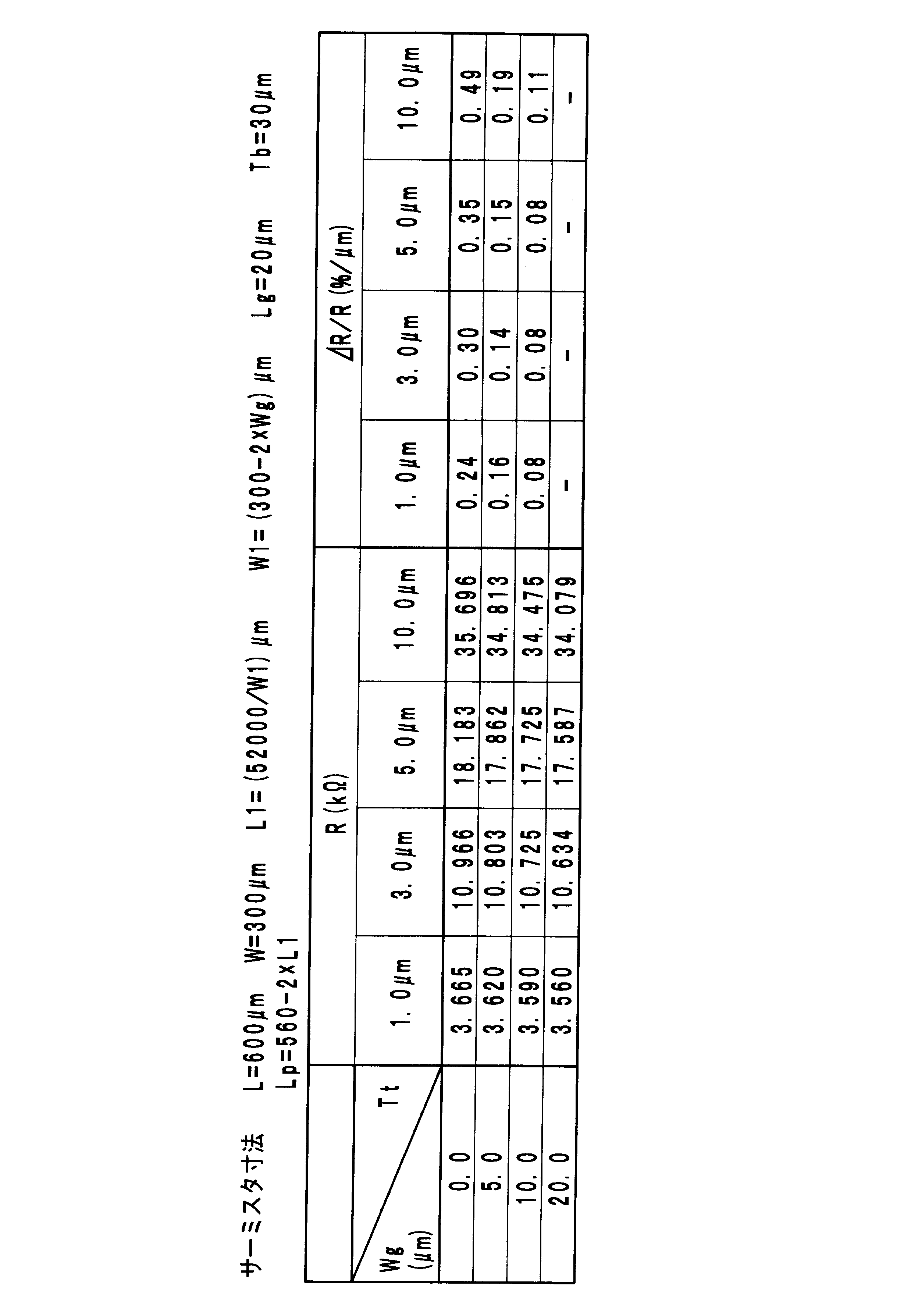
- the resistance value at room temperature was also obtained by simulation for the end face distance Lg of the divided electrodes.
- the end face distance Lg is 0.0-20.0 ⁇ m and the thickness Tt of the thermistor thin film layer is changed in the range of 1.0-10.0 ⁇ m
- the room temperature resistance value R (k ⁇ ) and the resistance change rate ⁇ R / R ( % / ⁇ m) is shown in Table 4 below.
- the side distance Wg is 20 ⁇ m, and other numerical values are listed in the margins of Table 4.
- the resistance value was also obtained by simulation for the side distance Wg of the divided electrodes.
- Room temperature resistance value R (k ⁇ ) and resistance change rate ⁇ R / R (when the side surface distance Wg is 0.0-20.0 ⁇ m and the thermistor thin film layer thickness Tt is changed in the range of 1.0-10.0 ⁇ m. % / ⁇ m) is shown in Table 5 below.
- the end face distance Lg is 20 ⁇ m, and other numerical values are described in the column of Table 5.
- the resistance change rate ⁇ R / R is preferably less than ⁇ 0.2%. That is, it is preferable to secure the distances Lg and Wg of 5 ⁇ m or more, and the influence of resistance change due to surface leakage at the end face and the side face can be prevented.
- the material has the same structure as that of the first embodiment shown in FIG. 1, and materials shown in Table 6 and Table 7 below are prepared.
- Tb 30 ⁇ m
- L A thermistor with 600 ⁇ m
- W 300 ⁇ m
- L1 200 ⁇ m
- W1 260 ⁇ m
- Lg 20 ⁇ m
- Wg 20 ⁇ m
- Lp 160 ⁇ m
- Tt 5 ⁇ m was produced.
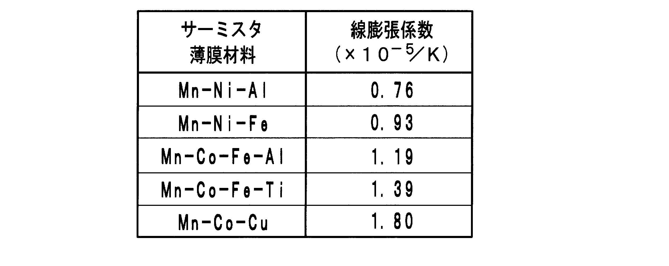
- the linear expansion coefficient shown in Table 6 and Table 7 is a linear expansion by TMA in an air atmosphere by preparing a prism having a cross section of 2.0 mm ⁇ 2.0 mm and a length of 5.0 mm from a metal base material and a thermistor thin film material. It is the result of measuring the coefficient.
- the value of the linear expansion coefficient at 800 ° C. is shown with 30 ° C. as a reference. The measurement conditions were a heating rate of 10 ° C./min and a load of 10 gf.
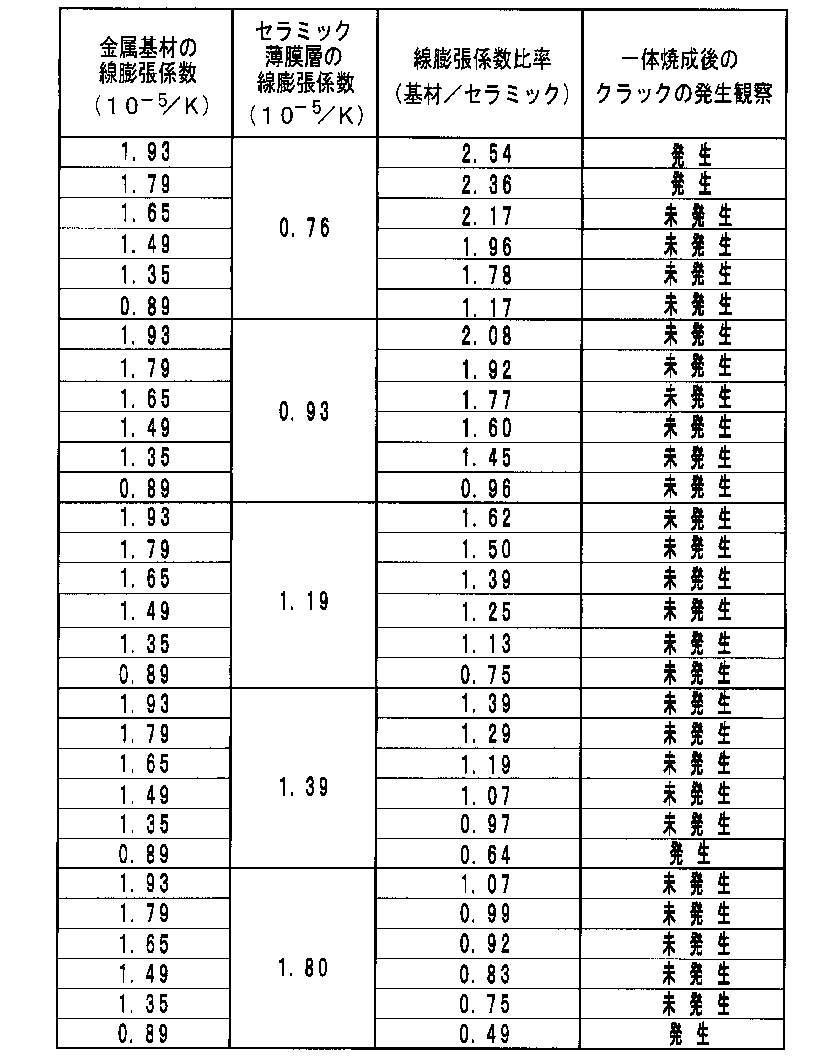
- the linear expansion coefficient ratio between the metal base material and the thermistor thin film material is set to 0.75 to 2.17, so that the linear expansion at the time of integral firing (particularly at the time of temperature reduction after firing). Generation of cracks due to the difference can be suppressed. Since ceramic materials are particularly vulnerable to tensile stress, cracks are likely to occur when they shrink faster than metal base materials (when the thermistor thin film material has a large linear expansion coefficient). Further, by making the linear expansion coefficient ratio of both materials within the above numerical range, it is possible to suppress the occurrence of cracks due to thermal stress when the thermistor is mounted on the substrate by reflow.
- the NTC thermistor 1B is composed of the metal base 11, the thermistor thin film layer 15, and the divided electrodes 21 and 22, as in the first embodiment.
- the protective layer 16 is formed on the thermistor thin film layer 15, and the Ni plating layer 23 and the Sn plating layer 24 are formed on the divided electrodes 21 and 22.
- the Ni plating layer 23 ′ and the Sn plating layer 24 ′ are also formed on the surface of the metal substrate 11, and these are formed simultaneously with the formation of the plating layers 23 and 24.
- the plated layers 23 ′ and 24 ′ can be expected to have an effect of preventing Ag migration when the metal substrate 11 is made of Ag / Pd or the like.
- the protective layer 16 suppresses the thermistor thin film layer 15 from being eroded by plating when the plated layers 23 and 24 are formed, and may be any insulating material that is not eroded by plating such as glass, resin, or insulating ceramic. .
- an insulating ceramic is used as the protective layer 16
- an insulating ceramic green sheet is previously formed on the thermistor thin film layer 15 when the metal substrate 11 and the thermistor thin film layer 15 are integrally fired.
- the metal substrate 11, the thermistor thin film layer 15 and the protective layer 16 can be formed by integral firing, the manufacturing process is simplified, and the adhesion between the thermistor thin film layer 15 and the protective layer 16 is improved.
- the thermistor 1B ′ shown in FIG. 6 is obtained by forming a protective layer 16 on the back surface and side surfaces of the metal substrate 11 with respect to the thermistor 1B shown in FIG.
- This kind of thermistor printed wiring board 40 is mounted on a land 41 formed on the surface by reflow through a solder 42.
- conductive parts, wirings, etc. may be electrically connected to the metal substrate 11.
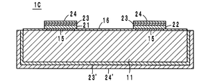
- the thermistor 1 ⁇ / b> C according to the fourth embodiment is such that the thermistor thin film layer 15 is formed in a rectangular shape just below the divided electrodes 21 and 22 and slightly smaller than the divided electrodes 21 and 22.
- the Ni plating layer 23 and the Sn plating layer 24 are formed on the divided electrodes 21 and 22 as in the third embodiment.
- the protective layer 16 is formed on the divided electrodes 21 and 22, in order to completely cover the thermistor thin film layer 15 with the protective layer 16, the divided electrodes 21, It is necessary to overlap the protective layer 16 around 22 (refer to part A in FIG. 5). In this case, in part A, the firing condition and sintering behavior of the protective layer 16 change due to the difference in the base, and cracks may occur in part A. Therefore, as in the fourth embodiment, the thermistor thin film layer 15 is provided immediately below the divided electrodes 21 and 22 and the protective layer 16 is provided on the same plane as the thermistor thin film layer 15 so that the underlying layer of the protective layer 16 is all metal. Since it becomes the base material 11 and the presence of the A portion which is an overlapping portion is eliminated, there is no possibility of occurrence of cracks, and the total thickness of the thermistor is reduced.
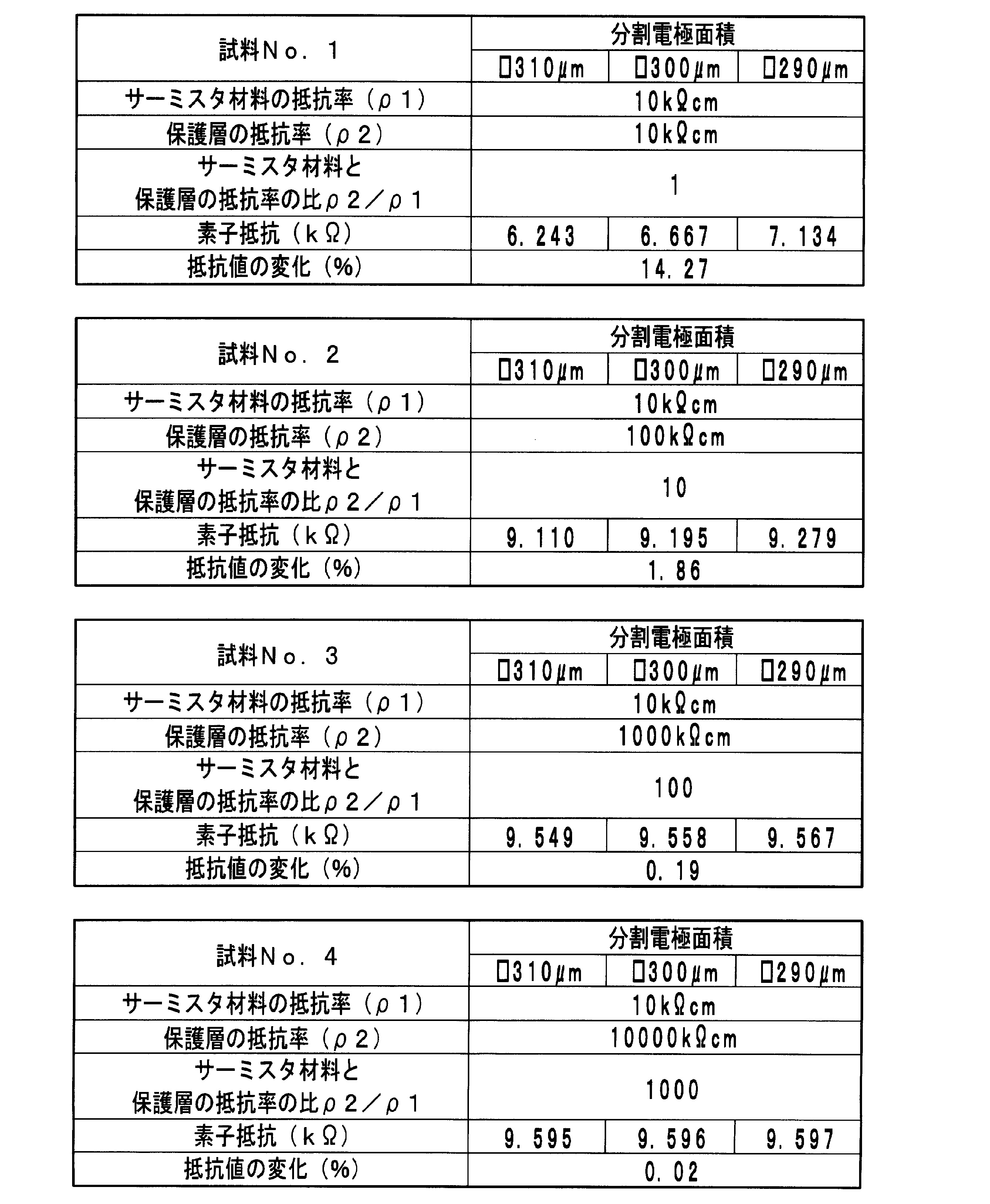
- the results of measuring the resistance value caused by the variation in the area of the divided electrodes 21 and 22 in the samples No1 to No4 shown in Table 9 are shown.
- the area (L1 ⁇ W1) of the divided electrodes 21 and 22 is 310 ⁇ m square, 300 ⁇ m square, and 290 ⁇ m square
- the thermistor material resistivity ⁇ 1 is 10 k ⁇ cm
- the protective layer 16 resistivity ⁇ 2 is The sample No. 1 was 10 k ⁇ cm
- the sample No2 was 100 k ⁇ cm
- the sample No3 was 1000 k ⁇ cm
- the sample No4 was 10,000 k ⁇ cm.
- ⁇ 1 is the resistivity of the thermistor material (specifically, Mn—Ni—Fe—Ti thermistor material) that becomes the thermistor thin film layer.
- ⁇ 2 is the resistivity of an insulating material (specifically, Fe—Mn ferrite material) serving as a protective layer, and the resistivity is changed by changing the composition ratio. The change rate (%) of the resistance value was calculated by the following formula.
- Resistance value change rate (R2 ⁇ R1) / R1 ⁇ 100
- R1 Element resistance value when the divided electrode area is 290 ⁇ m
- R2 Element resistance value when the divided electrode area is 310 ⁇ m
- the rate of change (%) in resistance value is 14.27 when ⁇ 2 / ⁇ 1 is 1 (sample No. 1), 1.86 when ⁇ 2 / ⁇ 1 is 10 (sample No. 2), When ⁇ 2 / ⁇ 1 was 100 (sample No. 3), it was 0.19, and when ⁇ 2 / ⁇ 1 was 1000 (sample No. 4), it was 14.27. It is preferable that ⁇ 2 / ⁇ 1 is 100 times or more because the rate of change in resistance value can be suppressed to 0.2% or less even if the areas of the divided electrodes 21 and 22 vary.
- the thermistor 1D according to the fifth embodiment has a thermistor thin film layer 15 having an area larger than that of the divided electrodes 21 and 22, in other words, a peripheral portion B of the thermistor thin film layer 15 is divided.
- the protective layer 16 is located on the outer side of the outer peripheral part of the electrodes 21 and 22 and covers the outer part B of the thermistor thin film layer 15 slightly inside.
- Other configurations are the same as those of the fourth embodiment.
- the protective layer 16 covers the outer peripheral portion B of the thermistor thin film layer 15, the thermistor thin film layer 15 is held by the protective layer 16 being in close contact with the metal substrate 11, and the thermistor thin film layer 15. Is prevented from peeling from the metal substrate 11. If the thermistor thin film layer 15 is peeled off from the metal base material 11, the region to which the resistance value contributes decreases, and the resistance value tends to increase. However, the present invention does not have such a concern. Since the protective layer 16 does not contribute to the thermistor characteristics, a material having high adhesion to the metal substrate 11 may be selected.
- the protective layer 16 is formed so as to partially overlap the outer peripheral portion of the thermistor thin film layer 15, and then the divided electrodes 21 and 22 are formed.
- the outer peripheral portion of the protective layer 16 is formed between the outer peripheral portion of the divided electrodes 21 and 22 on the thermistor thin film layer 15 side and the thermistor thin film layer 15.
- the split electrodes 21 and 22 may be cracked. Since the location (part A) is located apart, the divided electrodes 21 and 22 and the metal substrate 11 do not short-circuit.
- thermoistor and its manufacturing method concerning this invention are not limited to the said Example, It can change variously within the range of the summary.
- the various thermistor sizes shown in the above embodiments are merely examples.
- the metal substrate, the thermistor thin film layer, and the shape of the details of the divided electrodes are arbitrary.
- the present invention is useful for a thermistor and a method for manufacturing the thermistor, and is particularly excellent in that it can be mounted at a low height, reflowed, etc., can be manufactured at low cost, and can suppress the generation of cracks as much as possible. .
- Thermistor 11 Metal substrate 15 .
- Thermistor thin film layer 16 ... Protective layer (insulating layer) 21, 22 ... Divided electrodes 31 ... Carrier film
Landscapes
- Engineering & Computer Science (AREA)
- Microelectronics & Electronic Packaging (AREA)
- Physics & Mathematics (AREA)
- Manufacturing & Machinery (AREA)
- Electromagnetism (AREA)
- Nonlinear Science (AREA)
- General Physics & Mathematics (AREA)
- Thermistors And Varistors (AREA)
- Apparatuses And Processes For Manufacturing Resistors (AREA)
Abstract
Description
金属基材と、該金属基材上に形成されたサーミスタ薄膜層と、該サーミスタ薄膜層上に形成された一対の分割電極と、を備えたサーミスタの製造方法であって、
キャリアフィルム上にセラミックスラリーを所定の厚さに塗布して前記サーミスタ薄膜層となるセラミックグリーンシートを形成する工程と、
前記セラミックグリーンシート上に金属粉含有ペーストを所定の厚さに塗布して金属基材となる金属基材シートを形成する工程と、
前記セラミックグリーンシートの前記金属基材シートが形成された面と対向する面上に電極ペーストを所定の厚さに塗布して分割電極となる分割電極パターンを形成する工程と、
前記金属基材シート、前記セラミックグリーンシート、前記分割電極パターンを一体的に焼成する工程と、
を備えたことを特徴とする。
第1実施例であるNTCサーミスタ1Aは、図1に示すように、金属基材11と、該金属基材11上に形成されたサーミスタ薄膜層15と、該サーミスタ薄膜層15上に形成された一対の分割電極21,22とで構成されている。金属基材11は金属粉ペーストからシート状に形成され、サーミスタ薄膜層15はセラミックスラリーからシート状に形成され、分割電極21,22は電極材料ペーストを所定形状に形成したもので、これらの3者は一体的に焼成されている。なお、少なくとも金属基材11とサーミスタ薄膜層15とが一体焼成されればよい。
次に、前記サーミスタ1Aの製造工程について説明する。まず、サーミスタ薄膜層15の原料として、Mn-Ni-Fe-Tiの酸化物を所定の配合(抵抗率が104Ωcmとなることを目標とする)となるように秤量し、ボールミルにより、ジルコニアなどの粉砕媒体を用いて、十分に湿式粉砕し、その後、所定の温度で仮焼し、セラミック粉末を得た。
まず、巻付け試験を実施した。巻付け試験は、撓み量1mm、2mm、8mm、16mmでのサーミスタのそり量に相当する直径0.71cm、1.30cm、5.07cm、10.13cmの円筒に、長さ500mm、幅5mmのサーミスタ試験片を巻き付けて10秒間保持した。試験片において、金属基材の厚みTbは30μmとし、サーミスタ薄膜層の厚みTtは0.5~15.0μmとした。


R1:分割電極間距離がLp1のときの抵抗値
R2:分割電極間距離がLp2のときの抵抗値


第2実施例として、図1に示した第1実施例と同様の構成からなり、以下の表6及び表7に示す材料を用意し、前記同様の製造工程にて、Tb=30μm、L=600μm、W=300μm、L1=200μm、W1=260μm、Lg=20μm、Wg=20μm、Lp=160μm、Tt=5μmのサーミスタを作製した。なお、表6及び表7に示す線膨張係数は金属基材材料及びサーミスタ薄膜材料から断面2.0mm×2.0mm、長さ5.0mmの角柱を作製し、大気雰囲気にてTMAによる線膨張係数の測定を実施した結果である。30℃を基準として800℃での線膨張係数の値を示している。測定条件は、昇温速度10℃/min、荷重10gfとした。

第3実施例であるNTCサーミスタ1Bは、図5に示すように、金属基材11、サーミスタ薄膜層15、分割電極21,22からなることは前記第1実施例と同様であり、それに加えて、サーミスタ薄膜層15上に保護層16を形成し、かつ、分割電極21,22上にNiめっき層23及びSnめっき層24を形成したものである。
図6に示すサーミスタ1B'は、図5に示した前記サーミスタ1Bに対して、保護層16を金属基材11の裏面や側面にも形成したものである。この種のサーミスタプリント配線基板40の表面に形成したランド41上にはんだ42を介してリフローによって実装される。このとき、金属基材11が表面に露出していると、図示しない導電性の部品や配線などが金属基材11と導通してしまうおそれがある。このように分割電極21,22を除くサーミスタの全面を保護層(絶縁層)16で覆うことにより、このような短絡事故を未然に防止することができる。
第4実施例であるサーミスタ1Cは、図7に示すように、サーミスタ薄膜層15を分割電極21,22の直下に、分割電極21,22よりも僅かに小さい矩形状に形成したものである。分割電極21,22上にはNiめっき層23及びSnめっき層24が形成されていることは、前記第3実施例と同様である。
R1:分割電極面積が290μmのときの素子抵抗値
R2:分割電極面積が310μmのときの素子抵抗値
第5実施例であるサーミスタ1Dは、図8に示すように、サーミスタ薄膜層15の面積を分割電極21,22の面積よりも大きくしたもの、換言すると、サーミスタ薄膜層15の外周部分Bを分割電極21,22の外周部分よりも外側に位置させたもので、保護層16はサーミスタ薄膜層15の外周部分Bから若干内側まで覆っている。他の構成は第4実施例と同様である。
なお、本発明に係るサーミスタ及びその製造方法は前記実施例に限定するものではなく、その要旨の範囲内で種々に変更することができる。
11…金属基材
15…サーミスタ薄膜層
16…保護層(絶縁層)
21,22…分割電極
31…キャリアフィルム
Claims (12)
- 金属基材と、該金属基材上に形成されたサーミスタ薄膜層と、該サーミスタ薄膜層上に形成された一対の分割電極と、を備えたことを特徴とするサーミスタ。
- 前記金属基材の厚みが10~80μm、前記サーミスタ薄膜層の厚みが1~10μmであること、を特徴とする請求項1に記載のサーミスタ。
- 前記分割電極間の距離をLp、前記サーミスタ薄膜層の厚みをTtとしたとき、Lp≧Tt+5μmであること、を特徴とする請求項1又は請求項2に記載のサーミスタ。
- 前記分割電極の端部から前記サーミスタ薄膜層の端部までの距離が5μm以上であること、を特徴とする請求項1ないし請求項3のいずれかに記載のサーミスタ。
- 前記金属基材と前記サーミスタ薄膜層の線膨張係数の比が、0.75~2.17であること、を特徴とする請求項1ないし請求項4のいずれかに記載のサーミスタ。
- 前記金属基材は金属粉ペーストからシート状に形成され、前記サーミスタ薄膜層はセラミックスラリーからシート状に形成されていること、を特徴とする請求項1ないし請求項5のいずれかに記載のサーミスタ。
- 前記シート状の金属基材と前記シート状のサーミスタ薄膜層は一体的に積層した状態で焼成されたものであること、を特徴とする請求項6に記載のサーミスタ。
- 前記サーミスタ薄膜層の少なくとも分割電極が形成されている面に絶縁材料からなる保護層が形成されていることを特徴とする請求項1ないし請求項7に記載のサーミスタ。
- 前記サーミスタ薄膜層となるサーミスタ材料と、前記保護層となる絶縁体材料の抵抗率の差が100倍以上であることを特徴とする請求項8に記載のサーミスタ。
- 前記サーミスタ薄膜層が、それぞれの前記分割電極に対応して分割して形成されており、前記サーミスタ薄膜層の外周部分が前記分割電極の外周部分よりも外側に位置していることを特徴とする請求項1ないし請求項9に記載のサーミスタ。
- 前記分割電極のうち前記サーミスタ薄膜層側の位置する外周部分と、前記サーミスタ薄膜層との間に前記保護層の外周部分が形成されていることを特徴とする請求項8または請求項9に記載のサーミスタ。
- 金属基材と、該金属基材上に形成されたサーミスタ薄膜層と、該サーミスタ薄膜層上に形成された一対の分割電極と、を備えたサーミスタの製造方法であって、
キャリアフィルム上にセラミックスラリーを所定の厚さに塗布して前記サーミスタ薄膜層となるセラミックグリーンシートを形成する工程と、
前記セラミックグリーンシート上に金属粉含有ペーストを所定の厚さに塗布して金属基材となる金属基材シートを形成する工程と、
前記セラミックグリーンシートの前記金属基材シートが形成された面と対向する面上に電極ペーストを所定の厚さに塗布して分割電極となる分割電極パターンを形成する工程と、
前記金属基材シート、前記セラミックグリーンシート、前記分割電極パターンを一体的に焼成する工程と、
を備えたことを特徴とするサーミスタの製造方法。
Priority Applications (6)
| Application Number | Priority Date | Filing Date | Title |
|---|---|---|---|
| EP10811774.8A EP2472529B1 (en) | 2009-08-28 | 2010-08-20 | Thermistor and method for producing same |
| CN201080038323.XA CN102483978B (zh) | 2009-08-28 | 2010-08-20 | 热敏电阻及其制造方法 |
| JP2011528767A JP5375963B2 (ja) | 2009-08-28 | 2010-08-20 | サーミスタ及びその製造方法 |
| TW099128785A TWI517186B (zh) | 2009-08-28 | 2010-08-27 | Thermistor and its manufacturing method |
| US13/404,094 US8598975B2 (en) | 2009-08-28 | 2012-02-24 | Thermistor and method for manufacturing the same |
| US13/858,128 US8514050B1 (en) | 2009-08-28 | 2013-04-08 | Thermistor and method for manufacturing the same |
Applications Claiming Priority (2)
| Application Number | Priority Date | Filing Date | Title |
|---|---|---|---|
| JP2009-198024 | 2009-08-28 | ||
| JP2009198024 | 2009-08-28 |
Related Child Applications (1)
| Application Number | Title | Priority Date | Filing Date |
|---|---|---|---|
| US13/404,094 Continuation US8598975B2 (en) | 2009-08-28 | 2012-02-24 | Thermistor and method for manufacturing the same |
Publications (1)
| Publication Number | Publication Date |
|---|---|
| WO2011024724A1 true WO2011024724A1 (ja) | 2011-03-03 |
Family
ID=43627830
Family Applications (1)
| Application Number | Title | Priority Date | Filing Date |
|---|---|---|---|
| PCT/JP2010/064089 Ceased WO2011024724A1 (ja) | 2009-08-28 | 2010-08-20 | サーミスタ及びその製造方法 |
Country Status (6)
| Country | Link |
|---|---|
| US (2) | US8598975B2 (ja) |
| EP (1) | EP2472529B1 (ja) |
| JP (1) | JP5375963B2 (ja) |
| CN (1) | CN102483978B (ja) |
| TW (1) | TWI517186B (ja) |
| WO (1) | WO2011024724A1 (ja) |
Cited By (12)
| Publication number | Priority date | Publication date | Assignee | Title |
|---|---|---|---|---|
| WO2012114857A1 (ja) * | 2011-02-24 | 2012-08-30 | 株式会社村田製作所 | 電子部品の実装構造 |
| WO2013017531A1 (de) * | 2011-07-29 | 2013-02-07 | Epcos Ag | Verfahren zum herstellen eines elektrischen bauelements und elektrisches bauelement |
| WO2013073324A1 (ja) * | 2011-11-15 | 2013-05-23 | 株式会社村田製作所 | サーミスタおよびその製造方法 |
| JP2014109554A (ja) * | 2012-12-04 | 2014-06-12 | Murata Mfg Co Ltd | 赤外線センサおよびその製造方法 |
| CN104779022A (zh) * | 2014-01-09 | 2015-07-15 | 株式会社村田制作所 | 负特性热敏电阻及其制造方法 |
| US9797781B2 (en) | 2012-11-28 | 2017-10-24 | Murata Manufacturing Co., Ltd. | Thermistor device |
| DK179268B1 (en) * | 2011-06-01 | 2018-03-19 | Heraeus Sensor Technology Gmbh | Mass production of small temperature sensors with flip chips |
| JP2018535413A (ja) * | 2015-11-02 | 2018-11-29 | エプコス アクチエンゲゼルシャフトEpcos Ag | センサ素子およびセンサ素子を製造するための方法 |
| JP2019068287A (ja) * | 2017-10-02 | 2019-04-25 | 京セラ株式会社 | 圧電振動子 |
| JP2019068288A (ja) * | 2017-10-02 | 2019-04-25 | 京セラ株式会社 | 水晶振動子 |
| JP2019068286A (ja) * | 2017-10-02 | 2019-04-25 | 京セラ株式会社 | 圧電振動子 |
| WO2021261006A1 (ja) | 2020-06-26 | 2021-12-30 | 株式会社村田製作所 | サーミスタ |
Families Citing this family (14)
| Publication number | Priority date | Publication date | Assignee | Title |
|---|---|---|---|---|
| WO2013179774A1 (ja) * | 2012-05-28 | 2013-12-05 | 株式会社村田製作所 | Ntcサーミスタ素子およびその製造方法 |
| KR101886400B1 (ko) * | 2012-07-13 | 2018-08-08 | 세미텍 가부시키가이샤 | 박막 서미스터 소자 및 그 제조 방법 |
| WO2014128996A1 (ja) * | 2013-02-21 | 2014-08-28 | 株式会社村田製作所 | チップ型正特性サーミスタ素子 |
| US10912179B2 (en) | 2014-06-27 | 2021-02-02 | Belkin International, Inc. | Systems and methods for contextual intelligence using networked devices |
| US10194512B2 (en) | 2014-06-27 | 2019-01-29 | Belkin International Inc. | Network light switch with mechanical/electrical interface port |
| US9713231B2 (en) | 2014-06-27 | 2017-07-18 | Belkin International Inc. | Light switch controlling light source via wireless transmission |
| JP2016127467A (ja) * | 2015-01-06 | 2016-07-11 | セイコーエプソン株式会社 | 振動デバイス、電子機器及び移動体 |
| JPWO2017010216A1 (ja) * | 2015-07-15 | 2018-04-12 | 株式会社村田製作所 | 電子部品 |
| US10083781B2 (en) | 2015-10-30 | 2018-09-25 | Vishay Dale Electronics, Llc | Surface mount resistors and methods of manufacturing same |
| CN107389218A (zh) * | 2017-06-27 | 2017-11-24 | 苏州楚博生物技术有限公司 | 一种用于传感器的热敏材料 |
| US10438729B2 (en) | 2017-11-10 | 2019-10-08 | Vishay Dale Electronics, Llc | Resistor with upper surface heat dissipation |
| CN114041194B (zh) * | 2019-07-05 | 2023-08-22 | Tdk电子股份有限公司 | Ntc薄膜热敏电阻和制造ntc薄膜热敏电阻的方法 |
| JP7279574B2 (ja) * | 2019-08-09 | 2023-05-23 | 株式会社村田製作所 | 電子部品及び電子部品の製造方法 |
| CN112053822A (zh) * | 2020-09-04 | 2020-12-08 | 翔声科技(厦门)有限公司 | 一种负温度系数电阻器的制作工艺 |
Citations (4)
| Publication number | Priority date | Publication date | Assignee | Title |
|---|---|---|---|---|
| JPS61242002A (ja) * | 1985-04-19 | 1986-10-28 | 松下電器産業株式会社 | 薄膜サ−ミスタ |
| JPS61245502A (ja) | 1985-04-23 | 1986-10-31 | 松下電器産業株式会社 | 薄膜サ−ミスタ |
| JPS63310101A (ja) * | 1987-06-12 | 1988-12-19 | Nok Corp | 薄膜サ−ミスタの製造法 |
| JPH0590010A (ja) * | 1991-09-30 | 1993-04-09 | Matsushita Electric Ind Co Ltd | 厚膜サーミスタ |
Family Cites Families (20)
| Publication number | Priority date | Publication date | Assignee | Title |
|---|---|---|---|---|
| US3219480A (en) * | 1961-06-29 | 1965-11-23 | Gen Electric | Method for making thermistors and article |
| US3343114A (en) * | 1963-12-30 | 1967-09-19 | Texas Instruments Inc | Temperature transducer |
| GB1054525A (ja) * | 1965-02-03 | |||
| US3574930A (en) * | 1966-12-08 | 1971-04-13 | Gen Motors Corp | Method of forming a printed thermistor on a metal sheet |
| FR1602247A (ja) * | 1968-12-31 | 1970-10-26 | ||
| US4276535A (en) * | 1977-08-23 | 1981-06-30 | Matsushita Electric Industrial Co., Ltd. | Thermistor |
| JPH06162843A (ja) | 1992-09-22 | 1994-06-10 | Chodendo Hatsuden Kanren Kiki Zairyo Gijutsu Kenkyu Kumiai | Bi系酸化物超電導導体の製造方法 |
| AU693152B2 (en) | 1994-01-31 | 1998-06-25 | Nippon Tungsten Co., Ltd. | Flat PTC heater and resistance value regulating method for the same |
| JPH0862242A (ja) | 1994-07-29 | 1996-03-08 | Whitaker Corp:The | 加速度センサ |
| JP3284873B2 (ja) | 1996-03-27 | 2002-05-20 | 三菱マテリアル株式会社 | チップ型サーミスタの製造方法 |
| JPH1154301A (ja) * | 1997-08-07 | 1999-02-26 | Murata Mfg Co Ltd | チップ型サーミスタ |
| JPH11283803A (ja) | 1998-03-31 | 1999-10-15 | Murata Mfg Co Ltd | チップ抵抗器 |
| JP3597043B2 (ja) | 1998-04-17 | 2004-12-02 | 三菱マテリアル株式会社 | チップ型サーミスタの製造方法 |
| JP2001189201A (ja) * | 1999-12-27 | 2001-07-10 | Hayaki Denki:Kk | チップ型サーミスタおよびその製造方法 |
| TW583080B (en) * | 2001-03-07 | 2004-04-11 | Protectronics Technology Corp | Composite material for thermistor having positive temperature coefficient and manufacturing method thereof |
| TW543258B (en) * | 2001-10-08 | 2003-07-21 | Polytronics Technology Corp | Over current protection apparatus and its manufacturing method |
| JP2004039882A (ja) | 2002-07-04 | 2004-02-05 | Tateyama Kagaku Kogyo Kk | チップ型サーミスタとその製造方法 |
| JP2004069599A (ja) | 2002-08-08 | 2004-03-04 | Matsushita Electric Ind Co Ltd | 電子部品の製造方法とそれに用いるペースト |
| JP2006093565A (ja) | 2004-09-27 | 2006-04-06 | Kyocera Corp | 発光素子用配線基板ならびに発光装置およびその製造方法 |
| JP2007281400A (ja) * | 2006-04-04 | 2007-10-25 | Taiyo Yuden Co Ltd | 表面実装型セラミック電子部品 |
-
2010
- 2010-08-20 EP EP10811774.8A patent/EP2472529B1/en active Active
- 2010-08-20 CN CN201080038323.XA patent/CN102483978B/zh active Active
- 2010-08-20 JP JP2011528767A patent/JP5375963B2/ja active Active
- 2010-08-20 WO PCT/JP2010/064089 patent/WO2011024724A1/ja not_active Ceased
- 2010-08-27 TW TW099128785A patent/TWI517186B/zh active
-
2012
- 2012-02-24 US US13/404,094 patent/US8598975B2/en active Active
-
2013
- 2013-04-08 US US13/858,128 patent/US8514050B1/en active Active
Patent Citations (4)
| Publication number | Priority date | Publication date | Assignee | Title |
|---|---|---|---|---|
| JPS61242002A (ja) * | 1985-04-19 | 1986-10-28 | 松下電器産業株式会社 | 薄膜サ−ミスタ |
| JPS61245502A (ja) | 1985-04-23 | 1986-10-31 | 松下電器産業株式会社 | 薄膜サ−ミスタ |
| JPS63310101A (ja) * | 1987-06-12 | 1988-12-19 | Nok Corp | 薄膜サ−ミスタの製造法 |
| JPH0590010A (ja) * | 1991-09-30 | 1993-04-09 | Matsushita Electric Ind Co Ltd | 厚膜サーミスタ |
Non-Patent Citations (1)
| Title |
|---|
| See also references of EP2472529A4 |
Cited By (18)
| Publication number | Priority date | Publication date | Assignee | Title |
|---|---|---|---|---|
| WO2012114857A1 (ja) * | 2011-02-24 | 2012-08-30 | 株式会社村田製作所 | 電子部品の実装構造 |
| US9184362B2 (en) | 2011-02-24 | 2015-11-10 | Murata Manufacturing Co., Ltd. | Electronic-component mounting structure |
| DK179268B1 (en) * | 2011-06-01 | 2018-03-19 | Heraeus Sensor Technology Gmbh | Mass production of small temperature sensors with flip chips |
| US9230719B2 (en) | 2011-07-29 | 2016-01-05 | Epcos Ag | Method for producing an electrical component, and electrical component |
| WO2013017531A1 (de) * | 2011-07-29 | 2013-02-07 | Epcos Ag | Verfahren zum herstellen eines elektrischen bauelements und elektrisches bauelement |
| JP2014524154A (ja) * | 2011-07-29 | 2014-09-18 | エプコス アクチエンゲゼルシャフト | 電子デバイスの製造方法および電子デバイス |
| WO2013073324A1 (ja) * | 2011-11-15 | 2013-05-23 | 株式会社村田製作所 | サーミスタおよびその製造方法 |
| US9797781B2 (en) | 2012-11-28 | 2017-10-24 | Murata Manufacturing Co., Ltd. | Thermistor device |
| JP2014109554A (ja) * | 2012-12-04 | 2014-06-12 | Murata Mfg Co Ltd | 赤外線センサおよびその製造方法 |
| CN104779022A (zh) * | 2014-01-09 | 2015-07-15 | 株式会社村田制作所 | 负特性热敏电阻及其制造方法 |
| JP2018535413A (ja) * | 2015-11-02 | 2018-11-29 | エプコス アクチエンゲゼルシャフトEpcos Ag | センサ素子およびセンサ素子を製造するための方法 |
| US10788377B2 (en) | 2015-11-02 | 2020-09-29 | Epcos Ag | Sensor element and method for producing a sensor element |
| US10908030B2 (en) | 2015-11-02 | 2021-02-02 | Epcos Ag | Sensor element and method for producing a sensor element |
| JP2019068287A (ja) * | 2017-10-02 | 2019-04-25 | 京セラ株式会社 | 圧電振動子 |
| JP2019068288A (ja) * | 2017-10-02 | 2019-04-25 | 京セラ株式会社 | 水晶振動子 |
| JP2019068286A (ja) * | 2017-10-02 | 2019-04-25 | 京セラ株式会社 | 圧電振動子 |
| WO2021261006A1 (ja) | 2020-06-26 | 2021-12-30 | 株式会社村田製作所 | サーミスタ |
| US12500013B2 (en) | 2020-06-26 | 2025-12-16 | Murata Manufacturing Co., Ltd. | Thermistor |
Also Published As
| Publication number | Publication date |
|---|---|
| US8514050B1 (en) | 2013-08-20 |
| EP2472529A4 (en) | 2016-04-27 |
| TWI517186B (zh) | 2016-01-11 |
| US20130221584A1 (en) | 2013-08-29 |
| CN102483978A (zh) | 2012-05-30 |
| EP2472529B1 (en) | 2017-09-27 |
| JPWO2011024724A1 (ja) | 2013-01-31 |
| EP2472529A1 (en) | 2012-07-04 |
| TW201125001A (en) | 2011-07-16 |
| CN102483978B (zh) | 2015-03-11 |
| JP5375963B2 (ja) | 2013-12-25 |
| US20120188051A1 (en) | 2012-07-26 |
| US8598975B2 (en) | 2013-12-03 |
Similar Documents
| Publication | Publication Date | Title |
|---|---|---|
| JP5375963B2 (ja) | サーミスタ及びその製造方法 | |
| JP5668837B2 (ja) | 電子部品の実装構造 | |
| US9076576B2 (en) | Chip thermistor and thermistor assembly board | |
| US8994491B2 (en) | Chip resistor and method of manufacturing the same | |
| JP5652465B2 (ja) | チップバリスタ | |
| JP2018074143A (ja) | 抵抗素子及び抵抗素子アセンブリ | |
| JP5664760B2 (ja) | 電子部品の実装構造 | |
| JP6911754B2 (ja) | 電子部品および積層セラミックコンデンサ | |
| JP2011082064A (ja) | チップヒューズ | |
| CN100590755C (zh) | 可变电阻素体和可变电阻 | |
| JP2005197281A (ja) | 積層型チップバリスタ | |
| JP6911755B2 (ja) | 電子部品および積層セラミックコンデンサ | |
| JP4397279B2 (ja) | 抵抗組成物およびそれを用いた抵抗器 | |
| JP5240286B2 (ja) | チップサーミスタ及びチップサーミスタの製造方法 | |
| JP4492578B2 (ja) | バリスタ素体及びバリスタ | |
| CN121983401A (en) | Ceramic thermosensitive element | |
| JP6149649B2 (ja) | セラミック電子部品 | |
| CN121768783A (zh) | 一种热敏电阻元件及电子设备 | |
| JP4957155B2 (ja) | バリスタ | |
| JP2007026780A (ja) | 導電体ペースト、電子部品およびその製造方法 |
Legal Events
| Date | Code | Title | Description |
|---|---|---|---|
| WWE | Wipo information: entry into national phase |
Ref document number: 201080038323.X Country of ref document: CN |
|
| 121 | Ep: the epo has been informed by wipo that ep was designated in this application |
Ref document number: 10811774 Country of ref document: EP Kind code of ref document: A1 |
|
| WWE | Wipo information: entry into national phase |
Ref document number: 2011528767 Country of ref document: JP |
|
| REEP | Request for entry into the european phase |
Ref document number: 2010811774 Country of ref document: EP |
|
| WWE | Wipo information: entry into national phase |
Ref document number: 2010811774 Country of ref document: EP |
|
| NENP | Non-entry into the national phase |
Ref country code: DE |