WO2011040077A1 - 映像出力装置及び映像の合成方法 - Google Patents
映像出力装置及び映像の合成方法 Download PDFInfo
- Publication number
- WO2011040077A1 WO2011040077A1 PCT/JP2010/057590 JP2010057590W WO2011040077A1 WO 2011040077 A1 WO2011040077 A1 WO 2011040077A1 JP 2010057590 W JP2010057590 W JP 2010057590W WO 2011040077 A1 WO2011040077 A1 WO 2011040077A1
- Authority
- WO
- WIPO (PCT)
- Prior art keywords
- signal
- input video
- frame memory
- video signal
- input
- Prior art date
- Legal status (The legal status is an assumption and is not a legal conclusion. Google has not performed a legal analysis and makes no representation as to the accuracy of the status listed.)
- Ceased
Links
Images


Classifications
-
- H—ELECTRICITY
- H04—ELECTRIC COMMUNICATION TECHNIQUE
- H04N—PICTORIAL COMMUNICATION, e.g. TELEVISION
- H04N5/00—Details of television systems
- H04N5/222—Studio circuitry; Studio devices; Studio equipment
- H04N5/262—Studio circuits, e.g. for mixing, switching-over, change of character of image, other special effects ; Cameras specially adapted for the electronic generation of special effects
- H04N5/265—Mixing
-
- G—PHYSICS
- G06—COMPUTING OR CALCULATING; COUNTING
- G06F—ELECTRIC DIGITAL DATA PROCESSING
- G06F3/00—Input arrangements for transferring data to be processed into a form capable of being handled by the computer; Output arrangements for transferring data from processing unit to output unit, e.g. interface arrangements
- G06F3/14—Digital output to display device ; Cooperation and interconnection of the display device with other functional units
- G06F3/1423—Digital output to display device ; Cooperation and interconnection of the display device with other functional units controlling a plurality of local displays, e.g. CRT and flat panel display
- G06F3/1446—Digital output to display device ; Cooperation and interconnection of the display device with other functional units controlling a plurality of local displays, e.g. CRT and flat panel display display composed of modules, e.g. video walls
-
- G—PHYSICS
- G09—EDUCATION; CRYPTOGRAPHY; DISPLAY; ADVERTISING; SEALS
- G09G—ARRANGEMENTS OR CIRCUITS FOR CONTROL OF INDICATING DEVICES USING STATIC MEANS TO PRESENT VARIABLE INFORMATION
- G09G5/00—Control arrangements or circuits for visual indicators common to cathode-ray tube indicators and other visual indicators
- G09G5/36—Control arrangements or circuits for visual indicators common to cathode-ray tube indicators and other visual indicators characterised by the display of a graphic pattern, e.g. using an all-points-addressable [APA] memory
- G09G5/39—Control of the bit-mapped memory
- G09G5/395—Arrangements specially adapted for transferring the contents of the bit-mapped memory to the screen
- G09G5/397—Arrangements specially adapted for transferring the contents of two or more bit-mapped memories to the screen simultaneously, e.g. for mixing or overlay
-
- H—ELECTRICITY
- H04—ELECTRIC COMMUNICATION TECHNIQUE
- H04N—PICTORIAL COMMUNICATION, e.g. TELEVISION
- H04N5/00—Details of television systems
- H04N5/222—Studio circuitry; Studio devices; Studio equipment
- H04N5/262—Studio circuits, e.g. for mixing, switching-over, change of character of image, other special effects ; Cameras specially adapted for the electronic generation of special effects
-
- G—PHYSICS
- G09—EDUCATION; CRYPTOGRAPHY; DISPLAY; ADVERTISING; SEALS
- G09G—ARRANGEMENTS OR CIRCUITS FOR CONTROL OF INDICATING DEVICES USING STATIC MEANS TO PRESENT VARIABLE INFORMATION
- G09G2360/00—Aspects of the architecture of display systems
- G09G2360/12—Frame memory handling
Definitions
- the present invention relates to a video output device, and in particular, when a plurality of input video signals are combined to output one video, even if there is a frame shift between the input video signals that are input, tearing occurs.
- the present invention relates to a video output device that can be suppressed.
- the video signal When transmitting a video signal with a high resolution, the video signal may not be transmitted with a single cable due to the large amount of data. At that time, it is necessary to divide and transmit one video signal into a plurality of cables.
- the video processing device may not be able to create a video signal because the processing capability of the video processing device is insufficient.
- the video signal is divided, a video signal is created by a plurality of video processing devices, and these may be transmitted by separate cables.
- Patent Document 1 discloses a video output apparatus that generates a single display video in which a display area for each input video is secured from a plurality of input videos, and displays the single display video.
- the selection of the user and the area of each video are performed in order to prevent the occurrence of tearing that occurs when the videos are output simultaneously.
- a method is disclosed in which a reference input video is selected based on a ratio or the like, and another input video is synchronized with the frame frequency of the reference input video. That is, when displaying a plurality of input images having different frame frequencies, a display image better for the user is output using any one of the plurality of input images as a main input image in accordance with a predetermined selection rule. It is disclosed.
- the tearing means that a video break occurs in the video displayed on the screen, and the moving object in the video appears to have a line at the break, for example.
- Patent Document 1 it is possible to suppress tearing that occurs when a plurality of videos having different frame frequencies are simultaneously displayed on one screen, but one video is divided. Later, tearing that occurs when re-synthesizes cannot be suppressed. In other words, it originally occurs when a video signal corresponding to one video is divided into a plurality of video signals and transmitted separately by a plurality of cables, for example, and then the video signals are combined again and displayed as one video. The tearing cannot be suppressed.
- the present invention has been made in view of such a conventional problem, and occurs when one video signal is divided into a plurality of video signals and then the divided video signals are combined and displayed as one video. It is an object of the present invention to provide a video output device and a video composition method capable of suppressing tearing.
- the video output apparatus of the present invention has a signal synthesis unit that synthesizes a plurality of input video signals, and outputs one video based on the video signal synthesized by the signal synthesis unit.
- the signal synthesis unit synthesizes the reference input video signal and the reference input video signal.
- the reference input video signal and the other input video signal are synthesized so that frames having a long overlap of frame periods are synthesized with the other input video signal.
- the video composition method of the present invention is a video composition method for synthesizing a plurality of input video signals and outputting one video, wherein one of the plurality of input video signals is output.
- a step of specifying a frame having a long overlap between frame periods in the reference input video signal and another input video signal combined with the reference input video signal And a step of synthesizing the frames specified in the above steps.
- the plurality of input video signals are synthesized such that frames having a long overlap of the frame periods are synthesized with respect to the plurality of input video signals.
- the phases of the input video signals may be shifted. This shift is generally due to a difference in the length of the input cable connected to the video output device, a shift in timing when the input video signal is output, or the like. Usually, the phase shift is usually within plus or minus 0.5 frames.
- frames having a long overlap of frame periods are synthesized for a plurality of input video signals. For this reason, frames that do not correspond to each other are hardly synthesized, and tearing that is likely to occur when frames that do not correspond to each other are synthesized is less likely to occur.
- the signal synthesis unit when one input video signal among a plurality of input video signals is used as a reference input video signal, the signal synthesis unit synthesizes the reference input video signal and the reference input video signal.
- the reference input video signal and the other input video signal are synthesized such that frames having a long overlap of frame periods are synthesized with the other input video signal.
- the video composition method according to the present invention is such that when one input video signal of a plurality of input video signals is used as a reference input video signal, the reference input video signal is combined with the reference input video signal.
- the method includes a step of specifying a frame having a long overlap of frame periods and a step of synthesizing the frames specified in the above step.
- the video output device or the video synthesis method suppresses tearing that occurs when one video signal is divided into a plurality of video signals and then the divided video signals are combined and displayed as one video. There is an effect that it is possible to do.
- FIG. 8 is an explanatory diagram of an embodiment in which a lead frame number is generated by a lead frame number generation unit shown in FIG. 7. It is a block diagram which shows schematic structure of the video output device in Embodiment 4 of this invention.
- (A) is a figure which shows the state at the time of dividing
- (b) is dividing the frame memory of the video output device in Embodiment 1 or 2 of this invention into 2 frames
- FIG. 6C is an example diagram showing the generation result of the write frame number and the read frame number in the case where the frame memory is used, and (c) is a case where the frame memory of the video output device in Embodiment 3 or 4 of the present invention is divided into three frames. It is an example figure which shows the production
- (A) is an example figure which shows the production
- (b) is an example of the video output apparatus in FIG. It is an example figure which shows the production
- the plurality of input video signals input are asynchronous because they are combined into one video, and there is a shift between the video signals. Even so, a video output device that can reduce the tearing of the output video is provided.
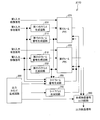
- FIG. 2 is a block diagram for illustrating a schematic configuration of the video output apparatus 1 according to the present embodiment.
- the video output apparatus 1 includes a signal synthesizer 10 that synthesizes an input video signal as a main component, and in addition to the signal synthesizer 10, a video input terminal, a video output terminal, and a power source (not shown).
- the signal synthesis unit 10 includes a first write address generation circuit 101 and a second write address generation circuit 102, a write frame number generation unit 110, a first frame memory 121 and a second frame memory 122, and an output timing signal generation circuit 130.
- the first write address generation circuit 101, the second write address generation circuit 102, and the write frame number generation unit 110 function as a writing unit that writes the input video signal to the frame memory.
- the output timing signal generation circuit 130, the read address generation circuit 140, the lead frame number generation unit 150, and the composite video signal output circuit 160 function as a reading unit that reads the input video signal written in the frame memory.
- the first and second assigned to each circuit name correspond to the first input video signal and the second input video signal, respectively, in which the video signal is divided into two.
- Each write address generation circuit counts two input valid signals and generates a write address for each.
- the input valid signal is a signal corresponding to an input video signal that is a video signal input to the video output device, and is a signal that validates a period in which the video signal exists in the input video signal.
- the input video signal is a signal that validates the period excluding the horizontal blanking period.
- the input video signal is divided into two input video signals, for example, an input video signal corresponding to the upper stage and an input video signal corresponding to the lower stage on the display screen.
- the input valid signal includes a first input valid signal and a second input valid signal corresponding to each.
- the first write address generation circuit 101 to which the first input valid signal is input and the second input valid signal are provided.
- An input second write address generation circuit 102 is provided.
- the light frame number generation unit 110 takes the AND of the input valid signals, which are signals indicating the valid range of the input video signals, for two input video signals and counts the valid periods of the signals.
- the light frame number is generated in the input video signal so that the input video signal of the longest period can be stored in the same frame. Therefore, the light frame number generation unit 110 receives the first input video signal and the second dominant video signal.
- the AND of the valid signal is to obtain a period during which the two input valid signals are on.
- the frame memory is a memory for writing an input video signal at a position specified by the write address and the write frame number.
- the input video signal includes the first input video signal and the second input video signal
- two frame memories are provided corresponding to the respective input video signals. Specifically, a first frame memory 121 to which a first input video signal is input and a second frame memory 122 to which a second input video signal is input are provided.
- the first frame memory 121 receives the write address from the first write address generation circuit 101 and the write frame number from the write frame number generation unit 110.
- the write address from the second write address generation circuit 102 and the write frame number from the write frame number generation unit 110 are input to the second frame memory 122.
- the output timing signal generation circuit 130 generates an output timing signal so that each input video signal is output in a preset order in synchronization with the timing signal.
- the read address generation circuit 140 counts the generated output timing signal and generates a read address.
- the lead frame number generation unit 150 generates a frame number when reading a video signal from the first frame memory 121 and the second frame memory 122.
- the read address and the lead frame number generated as described above are input and stored in each frame memory (first frame memory 121 and second frame memory 122).
- the synthesized video signal output circuit 160 reads the input video signals from the position (frame memory area) designated by the read address and the lead frame number from the first frame memory 121 and the second frame memory 122, And outputs a video signal according to the output timing.
- each frame memory is provided with a plurality of frame memory areas.
- This frame memory area corresponds to the capacity for one frame.
- Each frame memory area is numbered as an index for specifying each frame memory area.
- Designating the position by the read address and the lead frame number means, for example, designating the frame memory area by the index.
- the circuits other than the light frame number generation unit 110 have the same operations and operations as the corresponding circuits of a normal video output device, and thus description thereof is omitted. That is, in this embodiment, the operation and action of only the light frame number generation unit 110 will be described in detail.
- FIG. 1 is a block diagram showing a schematic configuration of the light frame number generation unit 110 in FIG.
- the light frame number generation unit 110 includes an extension circuit (111, 112) for extending an input valid signal (first and second input valid signals), an extended input valid signal ( An AND circuit 113 for ANDing the extended input valid signal), a counter 114 for counting a period during which the ANDed input valid signal is at a high level, and when the ANDed valid signal is changed from a high level to a low level.
- the maximum value detection circuit 115 for comparing the previous maximum value by the counter 114 with the current maximum value and outputting the input number according to the comparison result, and the input video based on the input number output from the maximum value detection circuit 115
- a frame number counter 116 for determining the light frame number for the signal and outputting the light frame number is provided.
- the video output apparatus 1 (see FIG. 2) of the present embodiment has two input valid signals, the first input valid signal and the second input valid signal.
- the extension circuit is also provided with two extension circuits, a first extension circuit 111 to which the first input valid signal is input and a second extension circuit 112 to which the second input valid signal is input. .
- the first extended circuit 111 outputs a first extended input valid signal, which is a valid signal obtained by extending the first input valid signal.
- the second extended circuit 112 outputs the second extended valid signal.
- a second extended input valid signal that is a valid signal obtained by extending the input valid signal is output.
- the first extension input valid signal and the second extension input valid signal are input to the AND circuit 113, and the AND circuit 113 performs an AND operation on the first extension input valid signal and the second extension input valid signal. Is done.
- the ANDed result is output to the counter 114 and the maximum value detection circuit 115.
- first vertical synchronization signal and the second vertical synchronization signal which are vertical synchronization signals respectively corresponding to the first input video signal and the second input video signal, are the maximum value detection circuit 115 and the frame number. Input to the counter 116 is possible.
- the first light frame number and the second light frame number are output to the first frame memory 121 and the second frame memory 122 shown in FIG.
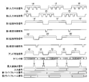
- the second input valid signal is input earlier than the first input valid signal within a predetermined range. That is, a case where the second input video signal is input earlier than the first input video signal for the corresponding input video signal will be described.
- valid signals..., 14, 15, 16... are input as the first input valid signals, and valid signals..., 24, 25, 26. .
- the valid signals 14 and 24, the valid signals 15 and 25, the valid signals 16 and 26,... It is assumed that the output is suppressed for tearing.
- the first input valid signal and the second input valid signal are respectively expanded by the first.
- the circuit 111 and the first extension circuit 112 are connected. Specifically, the first extension circuit 121 shown in FIG. 1 is used to extend the first input valid signal, and first extension signals including extension valid signals..., 14 ′, 15 ′, 16 ′. An input valid signal is generated, and the second input valid signal is expanded by the second expansion circuit 112 shown in FIG. 1 to include extended valid signals..., 24 ′, 25 ′, 26 ′, etc. as shown in FIG. A second extension input valid signal is generated.
- the vertical blanking period is detected, and vertical synchronizing signals respectively corresponding to the input numbers are generated.
- the vertical synchronization signal can be generated by a general technique in the art, a detailed description thereof will be omitted.
- a separately input signal may be used as the vertical synchronization signal.
- the first vertical synchronization signal and the second input valid signal correspond to the first input valid signal and the second input valid signal, respectively (corresponding to the first input video signal and the second input video signal, respectively).
- a second vertical synchronizing signal is generated.
- both the first extension input valid signal and the second extension input valid signal are input to the AND circuit 113 (see FIG. 1), and the AND circuit 113 takes the AND of the first and second extension valid signals.
- An AND valid signal is output.
- FIG. 3 when the extended input valid signal 14 ′ and the second extended input valid signal are ANDed, AND valid signals 41 and 42 are generated, and the extended input valid signal 15 ′ and the second extended input valid signal are generated.
- AND valid signals 51 and 52 are generated.
- an AND valid signal 61 is generated.
- an AND valid signal is input to the counter 114 (see FIG. 1), and the counter 114 counts a valid period during which each AND valid signal is at a high level (AND is “1”). That is, when the AND valid signal is at a low level (AND is “0”), it is not counted, and when it is at a high level, the counter is counted up by one unit.
- the maximum value of the counter value obtained by counting the AND valid signals 41, 51, 52 by the counter is 3
- the maximum value of the counter value obtained by counting the AND valid signals 42, 52, 62 is 6.
- the maximum value detection circuit 115 (see FIG. 1) caused the AND valid signal to change from a high level to a low level (that is, AND is “1” ⁇ “0”). At this point, the maximum value of the current counter that has counted the valid period of the AND valid signal is compared with the maximum value of the counter that has counted the valid period of the previous high AND valid signal.
- the counter stores the input number of the effective signal whose extended effective signal has changed.
- the counter outputs the stored input number to the frame number counter, and resets after storing the maximum value.
- the AND valid signals 41 and 42 will be described as an example.
- the comparison is the maximum value 3 of the counter value before counting the AND valid signal 41 and the maximum value of the current counter value after counting the AND valid signal 42. 6 is compared.
- the counter value of the AND valid signal 42 is the maximum, the extended valid signal at the time point when the AND “1” of the AND valid signal 42 becomes “0” (right terminal of the AND valid signal 42).
- Check for changes As a result of the confirmation, since it is confirmed that the extended input valid signal 24 has changed, the counter stores the input number 2 of the corresponding extended valid signal.
- the counter stores the first vertical synchronization signal. After the input number 2 is output to the frame number counter, the numerical value is reset, and the valid period of the next high-level AND valid signal 51 is counted.
- the signal currently counted is the AND valid signal 51
- the maximum value 3 of the counter value obtained by counting the AND valid signal 51, and the maximum value 6 of the counter value before the AND valid signal 42 is counted.
- the current counter value is not the maximum
- the current counter maximum value is stored, the numerical value is reset, and the next AND valid signal 52 is counted.
- the method for comparing the AND valid signal 52 and the AND valid signal 51 is also as described above.
- the input number of the upper and lower stage signals is determined by counting and comparing the valid period of the AND valid signal by the counter.
- the input number is a number assigned to each input video signal (or corresponding input valid signal) divided and input.
- the input number 1 and the input number 2 are described, but the present invention is not limited to this example. That is, any character may be used as long as it can be clearly described so as to distinguish a plurality of video signals.
- the frame number counter 116 (see FIG. 1) counts up the write frame number of the input video signal corresponding to the input number with reference to the vertical synchronization signal corresponding to the input number. Subsequently, based on the vertical synchronization signal (the other vertical synchronization signal) different from the vertical synchronization signal corresponding to the input number, the light frame number of the other input video signal is the same as the counted up number.
- the frame number counter 116 is a frame memory (shown in FIG. 1) corresponding to two write frame numbers (first write frame number and second write frame number) corresponding to each input number determined as described above. The data is output to the first frame memory 121 and the second frame memory 122).
- the second light frame from the time when the second vertical synchronization signal is input (the time when the signal level changes from “0” to “1”). Count up the number. That is, the light frame number assigned to the previous video signal is further counted up by one unit. Then, when the first vertical synchronization signal is input (when the signal level changes from “0” to “1”), the first light frame number is set to the same light frame number as the second light frame number.
- the light frame number is a frame memory that is attached to each of a plurality of input video signals so that one video is output by synthesizing video signals of the same frame number at the time of synthesis output. It is the number in.
- the light frame number generation unit assigns frame numbers to a plurality of video signals that are input asynchronously, synthesizes the video signals having the same frame number, and outputs them as one video.
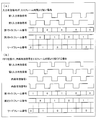
- the present embodiment is a case where a signal having the same shape as the video signal of the above embodiment is input, but the second input valid signal is within the predetermined range when the first input valid signal (first input video signal) is within a predetermined range.
- first input video signal first input video signal
- second input video signal A case where the input is made earlier than (second input video signal) will be described. That is, a case where the first input video signal is input earlier than the second input video signal for the corresponding input video signal will be described.
- the first input valid signal and the second input valid signal in the upper and lower stages are expanded, and an AND valid signal is generated by an AND circuit. Since the process up to counting the valid period of the AND valid signal by the counter is the same as that in the above embodiment, further explanation is omitted.
- the input order of the upper and lower video signals is different (reverse) from that in the above embodiment, so that the AND result of the first extended input valid signal and the second extended input valid signal, and the counter The value obtained by counting the valid period of the AND valid signal is different from that in the above embodiment.
- the counter 114 (see FIG. 1) counts the AND valid signals 41, 51, and 52 and the maximum counter value is 6, and the AND valid signals 42, 52, and 62 are counted.
- the maximum counter value is 3.
- the AND valid signals 41 and 42 will be described as an example.
- the maximum value 6 of the counter value before the AND valid signal 41 is counted is compared with the maximum value 3 of the current counter value after the AND valid signal 42 is counted. As a comparison result, since the current counter value is not the maximum, the next AND valid signal 51 is counted after resetting the numerical value.
- the maximum value detection circuit 115 (see FIG. 1) counts the AND valid signal 42 and stores the maximum value 3 of the previous counter value, and the maximum value 6 of the current counter value when the AND valid signal 51 is counted. And compare. In this comparison result, since the counter value of the AND valid signal 51 is the maximum, the extended input valid signal at the time point when the AND “1” of the AND valid signal 51 becomes “0” (the right terminal of the AND valid signal 51). 14 is confirmed to have changed, and the input number 1 of the corresponding valid signal is stored.
- the stored input number 1 When the first vertical synchronization signal, which is the vertical synchronization signal corresponding to the stored input number 1, is input, the stored input number 1 is output, and the valid period of the AND valid signal 51 by the counter Is reset, and the valid period of the next high level AND valid signal is counted.
- the frame number counter 116 determines the write frame number for each input video signal based on the first vertical synchronization signal corresponding to the input number 1, and uses the other vertical synchronization signal for the other vertical synchronization signal. The same frame number is output for the input video signal.
- the frame number counter 116 is a frame memory (shown in FIG. 1) corresponding to two write frame numbers (first write frame number and second write frame number) corresponding to each input number determined as described above.
- the data is output to the first frame memory 121 and the second frame memory 122).
- the light frame number generation unit 110 assigns frame numbers to a plurality of video signals that are input asynchronously, synthesizes the input video signals having the same frame number, and outputs them as one video. .
- FIG. 5 is a block diagram showing a schematic configuration of a video output device 1 ′ according to another embodiment of the present invention. As shown in FIG. 5, the video output device 1 ′ in the present embodiment is controlled by the video output device 1 in the first embodiment shown in FIG. 2, more specifically in the writing unit of the signal synthesis unit 10. And an arbitration circuit 170 as a unit.
- the video output device includes a first write address generation circuit 101 and a second write address generation circuit 102, a write frame number generation unit 110, an arbitration circuit 170, a frame memory 120, an output timing signal generation circuit 130, A read address generation circuit 140, a lead frame number generation unit 150, a composite video signal output circuit 160, and the like are provided.
- the parts other than the arbitration circuit 170 are substantially the same as those in the first embodiment, so the description will be outlined.
- the write address generation circuit (first write address generation circuit 101 and second write address generation circuit 102) counts two input valid signals (first input video signal and second input video signal), respectively.
- the write frame number generation unit 110 takes the AND of the input valid signal, which is a signal indicating the valid range of the input video signal, for the two input video signals, and validates the signal. The period is counted, and a light frame number is generated for the input video signal so that the video signal having the longest effective period can be stored in the same frame.
- the frame memory 120 is a memory for writing an input video signal at a position specified by the write address and the write frame number.
- two frame memories 121 and 122 are provided in accordance with the divided and input signals.
- the arbitration circuit 170 since the arbitration circuit 170 is installed in the preceding stage, even with one frame memory 120, the same effect as in the first embodiment can be obtained.
- the arbitration circuit 170 is installed in the preceding stage of the frame memory 120.
- the arbitration circuit 170 receives the input timing of each input video signal, the input timing of the write address, and the input video signal to the frame memory 120.
- control is performed so that each input video signal is sequentially written at the position specified by the write address and the write frame number.
- the output timing signal generation circuit 130 generates an output timing signal so that the input video signal is output in a preset order in synchronization with the timing signal, and the read address generation circuit 140 generates the generated output timing.
- the lead frame number generation unit 150 generates a frame number for reading a video signal from the frame memory, and the composite video signal output circuit 160 reads the read signal from the frame memory.
- the input video signal is read from the position specified by the address and the lead frame number, synthesized, and the video signal is output according to the output timing.
- the video output device 1 is configured by one frame memory by using an arbitration circuit. Therefore, the number of terminals and the number of parts of the entire apparatus can be reduced, and power consumption and cost can be reduced.
- each input video signal is written before writing (writing) each input video signal into which the single video is divided and input to the frame memory by the write frame number generation unit. Assign the same light frame number to the corresponding frame.
- reading (reading) from the frame memory a case has been described in which one video is output by reading and synthesizing input video signals with the same write frame number.
- each input video signal is not read at the stage of writing the input video signal to the frame memory but at the stage of reading each input video signal written to the frame memory from the frame memory.
- the video signal is divided into two will be described as an example.
- the lead frame number generation unit performs the same operation as that performed by the write frame number generation unit in the first and second embodiments.
- each input video signal into which one video is divided and input is not assigned the same light frame number, that is, a frame
- writing is performed without any special processing, and in the stage of reading out from the frame memory, synthesis and output as an appropriate video are realized.
- FIG. 6 is a block diagram showing a schematic configuration of the video output device 2 according to the present embodiment, more specifically, the signal synthesis unit 10.
- the video output device 2 includes a first write address generation circuit 201, a second write address generation circuit 202, a first write frame number generation unit 211, a second write frame number generation unit 212, and a first frame.
- a memory 221 and a second frame memory 222, an output timing signal generation circuit 230, a read address generation circuit 240, a lead frame number generation unit 250, a composite video signal output circuit 260, and the like are provided.
- the first write address generation circuit 201, the second write address generation circuit 202, the first write frame number generation unit 211, and the second write frame number generation unit 212 serve as a writing unit that writes the input video signal to the frame memory. Function.
- the output timing signal generation circuit 230, the read address generation circuit 240, the lead frame number generation unit 250, and the composite video signal output circuit 260 function as a reading unit that reads the input video signal written in the frame memory.
- the first write address generation circuit 201 and the second write address generation circuit 202 count the first input video signal and the second input video signal, respectively, and generate a write address for each.
- the first light frame number generation unit 211 and the second light frame number generation unit 212 write the first input video signal and the second input video signal to the first frame memory 221 and the second frame memory 222, respectively.
- a light frame number is generated in the video signal.
- the first frame memory 221 writes the first input video signal at the position specified by the write address and the write frame number
- the second frame memory 222 is written at the position specified by the write address and the write frame number. Write the second input video signal.
- the output timing signal generation circuit 230 generates an output timing signal so that each input video signal is output in a preset order in synchronization with the timing signal, and the read address generation circuit 240 generates the generated output.
- the timing signal is counted and a read address is generated.
- the lead frame number generator 250 counts the valid period of the first and second input video signals by taking the AND of the first and second input valid signals, which are signals indicating the valid range of the input video signals. Then, the lead frame number of each input video signal is determined so that the input video signals having the longest valid period can be simultaneously read from the corresponding frame memories.
- the read address and the lead frame number generated as described above are input to each frame memory (the first frame memory 221 and the second frame memory 222).
- the synthesized video signal output circuit 260 reads the input video signal from the position specified by the read address and the lead frame number from the first frame memory 221 and the second frame memory 222, synthesizes them, A video signal is output according to the output timing.
- FIG. 7 is a block diagram for illustrating a schematic configuration of the lead frame number generation unit 250.
- the lead frame number generation unit 250 includes first and second extension circuits 251 and 252 for extending the input first and second input valid signals, and an extended input valid signal ( An AND circuit 253 for ANDing the extended input valid signal), a first counter 254 for counting a period during which the ANDed input valid signal is at a high level, and the ANDed valid signal is changed from a high level to a low level.
- a maximum value detection circuit 255 for comparing the previous maximum value by the first counter 254 with the current maximum value and outputting the input number according to the comparison result is provided. These are the same as the light frame number generation unit in the first embodiment.
- the upper and lower first and second input valid signals are expanded by the first extension circuit 251 and the second extension circuit 252, respectively, and an AND valid signal is generated by the AND circuit 253, and As in the embodiment shown in FIG. 3, the first counter 254 counts the valid period of the AND valid signal and the count result is compared by the maximum value detection circuit 255.
- the lead frame number generation unit 250 includes a second counter 256a and a third counter 256b that count the valid periods of the first and second vertical synchronization signals respectively corresponding to the first and second input valid signals. Therefore, the first light frame number generation unit 211 (see FIG. 6) determines the first vertical sync signal when the first vertical synchronization signal changes from a low level to a high level (that is, the signal level changes from “0” to “1”). A first light frame number corresponding to the input video signal is generated and stored in the first frame memory 221. Similarly, the second light frame number generation unit 212 (see FIG. 6) determines that the second vertical synchronization signal is changed from the low level to the high level (that is, the signal level changes from “0” to “1”). A second light frame number corresponding to the 2-input video signal is generated and stored in the second frame memory 222.
- the lead frame number generation unit 250 includes a latch circuit for temporarily storing the frame number. The processing of each latch circuit will be described below.
- the lead frame number generation unit 250 uses the other input valid signal having the longest valid period between the write frame number of the input valid signal corresponding to the input number determined based on the processing of the maximum value detection circuit and the input valid signal.
- the signal write frame numbers are stored as one set, and the respective write frame numbers are stored in the first latch circuit 257a and the second latch circuit 257b, respectively.
- the write frame numbers temporarily stored in the first latch circuit 257a and the second latch circuit 257b are transferred to the third latch circuit 258a and the fourth latch circuit 258b, respectively, in accordance with the vertical synchronizing signal for reading. These are used as the first lead frame number and the second lead frame number, respectively.
- the lead frame number generation unit 250 stores the lead frame numbers of video signals of an appropriate combination to be combined as a set for a plurality of video signals input asynchronously. By synthesizing the input video signal having the lead frame number, one video without tearing is output.
- FIG. 9 is a block diagram showing a schematic configuration of a video output device 2 ′ according to another embodiment of the present invention. As shown in FIG. 9, the video output device 2 ′ in the present embodiment is controlled by the video output device 2 in the third embodiment shown in FIG. 6, more specifically in the write unit of the signal synthesis unit 10. And an arbitration circuit 270 as a unit.
- the arbitration circuit 270 has a function similar to that of the arbitration circuit 170 described in the second embodiment.
- the arbitration circuit 270 is installed in the previous stage of the frame memory 220.
- the arbitration circuit 270 adds the input timing of each input video signal, the input timing of the write address, and each input video signal to the frame memory 220. By adjusting the input timing of the write frame number, control is performed so that each input video signal is sequentially written at the position specified by the write address and the write frame number.
- the light frame number generation unit in the first and second embodiments generates first and second light frame numbers for the first and second input video signals, respectively.
- the first and second input video signals are sequentially assigned the light frame numbers consisting of “0” and “1”, respectively. To be assigned.
- the first light frame number and the second frame number are signals indicating effective ranges of two input video signals by the light frame number generation unit.
- An AND of the input valid signal is taken, the valid period of the signal is counted, and the first input video signal and the second input video signal are generated so that the input video signal with the longest valid period can be stored in the same frame.
- the light frame number is a signal indicating effective ranges of two input video signals by the light frame number generation unit.
- the first and second input video signals (input video signals having the same light frame number) having the light frame number “0” with hatched shading are combined, Output as one video.
- the lead frame number at that time is read.
- the first light frame number or the second light frame number may overlap.
- the write frame number corresponding to the lead frame number is not clear, even when the read frame number corresponding to one read frame number is read out, tearing occurs in the output video. There is.
- the lead frame number and the second write frame number are read out. Has an overlapping portion (“0”). Therefore, in the area A ′, the write frame number (“0”) for which writing has not been completed becomes the reading target.
- the present embodiment it is possible to solve the above problem that the read frame number and the write frame number overlap by dividing one frame memory into frame memory areas for three frames. .
- one frame memory is divided into frame memory areas for three frames including frame numbers 0, 1, and 2.
- the first and second light frame numbers are generated by switching in the order of “0” ⁇ “1” ⁇ “2” ⁇ “0”, Lead frame numbers corresponding to the first and second write frame numbers are generated.
- the lead frame number when reading a specific lead frame number, the lead frame number may overlap with the first and second write frame numbers. Does not occur.
- the first and second write frame numbers corresponding to the lead frame number are surely read. be able to.
- FIG. 11 is a signal display diagram for explaining a case where one frame memory is divided into frame memory areas for three frames in the video output devices according to the third and fourth embodiments.
- the first and second write frame numbers are generated in the order of “0” ⁇ “1” ⁇ “2” ⁇ “0”...
- the lead frame number generation unit is the same as in the third and fourth embodiments.
- a series of processing as described above is performed to determine the first and second light frame numbers as one set. Then, first and second lead frame numbers are generated corresponding to the first and second write frame numbers in accordance with the read vertical synchronization signal.
- the problem of the comparative example can be solved by adjusting the effective period of the input video signal.
- the effective period of the input video signal and the effective period of the output signal are less than 2/3 of one frame time, thereby solving the problem of the comparative example with a frame memory having a capacity of 2 frames. can do.
- the frame number is set to “0” even in the frame memory for two frames. By alternately switching from “1” to “0” to “1”..., It is possible to perform control so that the write operation and the read operation do not overlap in the frame memory having the same frame number.
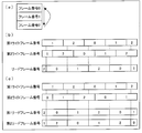
- FIG. 13A is a diagram illustrating the generation result of the write frame number and the read frame number when the effective period of the input video signal is adjusted to two thirds.
- blank portions portions without numerals indicate periods during which no writing or reading is performed.
- the capacity of two frames can be controlled so that the write frame number and the read frame number do not overlap.
- the frame memory cannot be reduced to 2 frames.
- the FIFO First In First Out: memory having first-in first-out characteristics
- FIG. 12 is a diagram showing a schematic configuration of the video display device 3 provided with the FIFO.
- the signal synthesizing unit 10 of the video display device 3 includes a first FIFO 371 (auxiliary memory) at the input unit of the first frame memory 321 and a third FIFO 373 (auxiliary memory) at the output unit. Is provided.
- a second FIFO 372 (auxiliary memory) is provided at the input portion of the second frame memory 322, and a fourth FIFO 374 (auxiliary memory) is provided at the output portion thereof.
- the input video signal corresponding to one third of the frame is temporarily stored in the first and second FIFOs 371 and 372, and the remaining two thirds are written in the frame memory. Therefore, in order to make the effective period of the input video signal less than 2/3, the size of each FIFO may be a maximum one-third frame.
- the input video signal corresponding to the third frame is read while being temporarily stored in the third and fourth FIFOs 373 and 374.
- FIG. 13B is a diagram similar to FIG. 13A, and shows the generation result of the write frame number and the read frame number when the FIFO is provided and the internal valid signal is shorter than 2/3 frame time. It is a figure illustrated.
- a FIFO is provided and the internal valid signal is made shorter than 2/3 frame time, so that the write frame number and the read frame number can be obtained in a frame memory having a capacity of 2 frames. Control that does not overlap can be performed.
- the overall configuration of the video apparatus in which the video output apparatus according to the present embodiment is used is not particularly limited.
- the following configuration is conceivable.
- a TV tuner (for example, connected to an antenna) is connected to the video output device as the first input (corresponding to the first input video signal), and the second input (corresponding to the second input video signal).
- a player such as a BD or DVD is connected.
- a configuration in which a display device such as a CRT, a liquid crystal display, or a PDP is connected as an output (corresponding to an output video signal) can be exemplified.
- the internal valid signal can be made shorter than 2/3 frame time by using the FIFO, the write frame number and the read frame number do not overlap in a frame memory having a capacity of 2 frames. You can control.
- the same effect can be obtained even if there are three or more inputs.
- the signal synthesis unit in the input video signal, when the period in which a signal based on video is input is an effective signal period, the signal synthesis unit includes the reference input video signal and the other input signal.
- the reference input video signal and the other input video signal are combined so that the effective signal periods having a long overlapping of the effective signal periods start at the same time, thereby overlapping the frame periods. Is characterized by synthesizing long frames.
- the reference input video signal and the other input video signal By specifying an effective signal period in which the overlapping of the effective signal periods is long, a frame in which the overlapping of the frame periods is long is specified.
- the frame to be synthesized is determined based on the overlap of the effective signal periods.
- the signal synthesis unit is provided with a frame memory in which the input video signal is written for each of the plurality of input video signals, and the input video signal is stored in the frame memory.
- the frame memory is provided with a plurality of frame memory areas, and the frame memory area is provided with an index for specifying each of the frame memory areas.
- the frame memory stores the input video signal so that frames having a long overlap in the frame period are written to the frame memory area with the same index in the frame memory corresponding to the input video signal. It is characterized by writing in.
- the corresponding frame is written to the frame memory area with the same index.
- the corresponding frames can be synthesized by determining a single read address, for example, without performing any special operation.
- the signal synthesizing unit is provided with a frame memory in which the input video signal is written for each of the plurality of input video signals.
- a readout unit for reading out the input video signal is provided, the frame memory is provided with a plurality of frame memory areas, and the frame memory area is provided with an index for specifying each of the frame memory areas,
- the reading unit determines the index of the frame memory area to be read in the frame memory corresponding to each input video signal so that frames having a long overlap of the frame periods are read simultaneously.
- the writing of the video signal to the frame memory can be simplified, and for example, high-speed writing can be performed.
- a single frame memory in which a plurality of the input video signals can be written in the signal synthesizer, and a plurality of the input videos to the single frame memory.
- a writing control unit that controls writing in order so that signal writing timings do not overlap.
- the write control unit for controlling the write timing of the input video signal.
- a plurality of input video signals can be written in a single frame memory. Therefore, the configuration of the video output device can be simplified, and the manufacturing cost can be reduced.
- the signal synthesis unit includes a frame memory in which the input video signal is written for each of the plurality of input video signals, and a writing unit that writes the input video signal to the frame memory. And a reading unit for reading the input video signal written in the frame memory.
- the frame memory includes three frame memory areas, and each frame memory area includes the above-described frame memory area. An index for identifying each frame memory area is attached, and the writing unit and the reading unit are not simultaneously written to and read from the frame memory area with the same index. As described above, the writing and reading are performed. According to the above configuration, the frame memory is provided with three frame memory areas. For this reason, writing and reading are not performed simultaneously on the frame memory areas assigned the same index. Therefore, occurrence of tearing in the frame can be suppressed.
- One frame memory area has a capacity corresponding to the data amount of one frame of the input video signal.
- the signal synthesis unit includes a frame memory in which the input video signal is written for each of the plurality of input video signals, and a writing unit that writes the input video signal to the frame memory. And a reading unit for reading the input video signal written in the frame memory.
- the frame memory has two frame memory areas, and each frame memory area has the above-mentioned When an index for identifying each frame memory is attached, and the period in which a signal based on video is input in the input video signal is an effective signal period, the effective signal period is 3 of the frame period.
- the write unit and the read unit are less than two parts of the frame memory area with the same index. As not performed and the write and read simultaneously, and performs the above-described writing and reading.
- the signal synthesis unit includes a frame memory in which the input video signal is written for each of the plurality of input video signals, and a writing unit that writes the input video signal to the frame memory.
- Auxiliary memories each having a first-in first-out characteristic are provided, and the auxiliary memory has a capacity for storing an input video signal corresponding to a period of one third or more of the frame period.
- the frame memory has two frame memory areas, and each frame memory area has a An index for specifying is attached, and the writing unit and the reading unit are configured so that the writing and reading are not performed simultaneously on the frame memory area to which the same index is attached. It is characterized by performing writing and reading.
- the auxiliary memory corresponding to the effective signal period of the input video signal is less than 2/3 of the frame period or more than one third of the frame period is provided.
- control program of the present invention causes a computer to function as the signal synthesizer.
- control program is stored in the computer-readable recording medium of the present invention.
- the present invention can be suitably used for a video apparatus that transmits a high-resolution video by dividing it into a plurality of cables.
Landscapes
- Engineering & Computer Science (AREA)
- Multimedia (AREA)
- Theoretical Computer Science (AREA)
- General Physics & Mathematics (AREA)
- Signal Processing (AREA)
- Physics & Mathematics (AREA)
- Human Computer Interaction (AREA)
- General Engineering & Computer Science (AREA)
- Computer Hardware Design (AREA)
- Controls And Circuits For Display Device (AREA)
- Studio Circuits (AREA)
- Television Systems (AREA)
- Image Processing (AREA)
Abstract
Description
図2は、本実施の形態の映像出力装置1の概略構成示すためのブロック図である。同図に示すように、映像出力装置1は、入力映像信号を合成する信号合成部10を主な構成要素とし、上記信号合成部10の他に、図示しない映像入力端子,映像出力端子,電源部等を有している。そして、上記信号合成部10は、第1ライトアドレス生成回路101と第2ライトアドレス生成回路102、ライトフレーム番号生成部110、第1フレームメモリ121と第2フレームメモリ122、出力タイミング信号生成回路130、リードアドレス生成回路140、リードフレーム番号生成部150、及び合成映像信号出力回路160などを備えている。
以下、図1,3に基づいて、ライトフレーム番号生成部110によりライトフレーム番号を決める手順を具体的に説明する。
以下、図1,4に基づいて、ライトフレーム番号を決める手順の他の例を説明する。ここでも、1つの映像を2つのケーブルに分割して伝送する場合、すなわち、入力映像信号が上下段の2部分に分けられた場合を例として説明する。
図5は、本発明の他の実施の形態による映像出力装置1’の概略構成を示すブロック図である。図5に示すように、本実施の形態における映像出力装置1’は、図2に示す上記実施の形態1における映像出力装置1に、より詳しくは上記信号合成部10の書き込み部に、書き込み制御部としての調停回路170をさらに備えた構成を有している。
以下、図6~8に基づいて、本発明の他の実施形態による映像出力装置の構成及び動作を説明する。
〔実施の形態4〕
図9は、本発明の他の実施の形態による映像出力装置2’の概略構成を示すブロック図である。図9に示すように、本実施の形態における映像出力装置2’は、図6に示す上記実施の形態3における映像出力装置2に、より詳しくは上記信号合成部10の書き込み部に、書き込み制御部としての調停回路270をさらに備えた構成を有している。
上記実施の形態1~4では、1つの映像を複数の入力映像信号に分割して送信する場合、各入力映像信号の間に発生するテアリング、すなわちフレーム間のテアリングを抑制することができる。
上記実施の形態5の比較例に説明したように、フレームメモリを2フレーム分のフレームメモリ領域に分割した場合、リードフレーム番号と、ライトフレーム番号とには重なる場合が生じるので、複数に分割された入力映像信号が正確に合成できず、テアリングが発生することがある。そして、上記実施の形態5の実施例として説明したように、フレームメモリを3フレーム分のフレームメモリ領域に分割すると上記問題を解決することが可能である。
1’映像出力装置
2 映像出力装置
2’映像出力装置
3 映像出力装置
10 信号合成部
121 第1フレームメモリ(フレームメモリ)
122 第2フレームメモリ(フレームメモリ)
221 第1フレームメモリ(フレームメモリ)
222 第2フレームメモリ(フレームメモリ)
220 フレームメモリ
321 第1フレームメモリ(フレームメモリ)
322 第2フレームメモリ(フレームメモリ)
371 第1FIFO(補助メモリ)
372 第2FIFO(補助メモリ)
373 第3FIFO(補助メモリ)
374 第4FIFO(補助メモリ)
Claims (12)
- 複数の入力映像信号を合成する信号合成部を有し、上記信号合成部で合成された映像信号に基づいて1つの映像を出力する映像出力装置であって、
上記複数の入力映像信号の内の1つの入力映像信号を基準入力映像信号とした場合、
上記信号合成部は、上記基準入力映像信号と、上記基準入力映像信号と合成される他の入力映像信号とにおいて、互いのフレーム期間の重なり合いが長いフレーム同士が合成されるように、上記基準入力映像信号と上記他の入力映像信号とを合成することを特徴とする映像出力装置。 - 上記入力映像信号において、映像に基づく信号が入力されている期間を有効信号期間とした場合、
上記信号合成部は、上記基準入力映像信号と、上記他の入力映像信号とにおいて、互いの上記有効信号期間の重なり合いが長い有効信号期間同士が同時開始するように上記基準入力映像信号と上記他の入力映像信号とを合成することで、上記フレーム期間の重なり合いが長いフレーム同士を合成することを特徴とする請求項1に記載の映像出力装置。 - 上記信号合成部には、複数の上記入力映像信号ごとに、上記入力映像信号が書き込まれるフレームメモリが設けられているとともに、上記フレームメモリに上記入力映像信号を書き込む書き込み部が設けられており、
上記フレームメモリには、複数のフレームメモリ領域が設けられており、
上記フレームメモリ領域には、それぞれを特定するための指標が付されており、
上記書き込み部は、上記フレーム期間の重なり合いが長いフレーム同士が、それぞれの上記入力映像信号に対応する上記フレームメモリにおける同じ指標が付された上記フレームメモリ領域に書き込まれるように、上記入力映像信号を上記フレームメモリに書き込むことを特徴とする請求項1又は2に記載の映像出力装置。 - 上記信号合成部には、複数の上記入力映像信号ごとに、上記入力映像信号が書き込まれるフレームメモリが設けられているとともに、上記フレームメモリに書き込まれた上記入力映像信号を読み出す読み出し部が設けられており、
上記フレームメモリには、複数のフレームメモリ領域が設けられており、
上記フレームメモリ領域には、それぞれを特定するための指標が付されており、
上記読み出し部は、上記フレーム期間の重なり合いが長いフレーム同士が同時に読み出されるように、それぞれの上記入力映像信号に対応する上記フレームメモリにおいて、読み出し先となるフレームメモリ領域の上記指標を決定することを特徴とする請求項1又は2に記載の映像出力装置。 - 上記信号合成部には、複数の上記入力映像信号を書き込むことが可能な単一のフレームメモリと、
単一の上記フレームメモリへの、複数の上記入力映像信号の書き込みタイミングが重ならないように順番に書き込むように制御する書き込み制御部とが設けられていることを特徴とする請求項1又は2に記載の映像出力装置。 - 上記信号合成部には、複数の上記入力映像信号ごとに、上記入力映像信号が書き込まれるフレームメモリと、
上記フレームメモリに上記入力映像信号を書き込む書き込み部と、
上記フレームメモリに書き込まれた上記入力映像信号を読み出す読み出し部とが設けられており、
上記フレームメモリには、3個のフレームメモリ領域が設けられているとともに、各フレームメモリ領域には、上記各フレームメモリ領域を特定するための指標が付されており、
上記書き込み部と上記読み出し部とは、同じ上記指標が付された上記フレームメモリ領域に対して、同時に書き込みと読み出しとが行われないように、上記書き込みと読み出しとを行うことを特徴とする請求項1から4の何れか1項に記載の映像出力装置。 - 上記信号合成部には、複数の上記入力映像信号ごとに、上記入力映像信号が書き込まれるフレームメモリと、
上記フレームメモリに上記入力映像信号を書き込む書き込み部と、
上記フレームメモリに書き込まれた上記入力映像信号を読み出す読み出し部とが設けられており、
上記フレームメモリには、2個のフレームメモリ領域が設けられているとともに、各フレームメモリ領域には、上記各フレームメモリを特定するための指標が付されており、
上記入力映像信号において、映像に基づく信号が入力されている期間を有効信号期間とした場合、上記有効信号期間は、上記フレーム期間の3分の2未満であり、
上記書き込み部と上記読み出し部とは、同じ上記指標が付された上記フレームメモリ領域に対して、同時に上記書き込みと読み出しとが行われないように、上記書き込みと読み出しとを行うことを特徴とする請求項2から4の何れか1項に記載の映像出力装置。 - 上記信号合成部には、複数の上記入力映像信号ごとに、上記入力映像信号が書き込まれるフレームメモリと、
上記フレームメモリに上記入力映像信号を書き込む書き込み部と、
上記フレームメモリに書き込まれた上記入力映像信号を読み出す読み出し部とが設けられており、
上記フレームメモリの上記入力映像信号の書き込み部分、及び、上記フレームメモリの上記入力映像信号の読み出し部分には、それぞれ先入れ先だし特性を有する補助メモリが設けられており、
上記補助メモリは、上記フレーム期間の3分の1以上の期間に対応する入力映像信号をメモリする容量を有しており、
上記フレームメモリには、2個のフレームメモリ領域が設けられているとともに、各フレームメモリ領域には、それぞれを特定するための指標が付されており、
上記書き込み部と上記読み出し部とは、同じ上記指標が付された上記フレームメモリ領域に対して、同時に上記書き込みと読み出しとが行われないように、上記書き込みと読み出しとを行うことを特徴とする請求項1から4の何れか1項に記載の映像出力装置。 - 請求項1に記載の信号合成部としてコンピュータを機能させることを特徴とする制御プログラム。
- 請求項9に記載の制御プログラムを格納したコンピュータ読取可能な記録媒体。
- 複数の入力映像信号を合成して1つの映像を出力する映像の合成方法であって、
上記複数の入力映像信号の内の1つの入力映像信号を基準入力映像信号とした場合、
上記基準入力映像信号と、上記基準入力映像信号と合成される他の入力映像信号とにおいて、互いのフレーム期間の重なり合いが長いフレームを特定するステップと、
上記ステップで特定されたフレーム同士を合成するステップとを有することを特徴とする映像の合成方法。 - 上記入力映像信号において、映像に基づく信号が入力されている期間を有効信号期間とした場合、
上記基準入力映像信号と、上記他の入力映像信号とにおいて、互いの上記有効信号期間の重なり合いが長い有効信号期間を特定することで、互いのフレーム期間の重なり合いが長いフレームを特定することを特徴とする請求項11に記載の映像の合成方法。
Priority Applications (6)
| Application Number | Priority Date | Filing Date | Title |
|---|---|---|---|
| US13/390,440 US20120140118A1 (en) | 2009-09-29 | 2010-04-28 | Image output device and image synthesizing method |
| JP2011534105A JP5280546B2 (ja) | 2009-09-29 | 2010-04-28 | 映像出力装置及び映像の合成方法 |
| EP10820197A EP2485475A1 (en) | 2009-09-29 | 2010-04-28 | Image output device and image synthesizing method |
| BR112012007573A BR112012007573A2 (pt) | 2009-09-29 | 2010-04-28 | dispositivo de saída de imagem e método de sintetização de imagem |
| CN2010800363344A CN102484680A (zh) | 2009-09-29 | 2010-04-28 | 视频输出装置和视频的合成方法 |
| RU2012108637/07A RU2012108637A (ru) | 2009-09-29 | 2010-04-28 | Устройство вывода изображения и способ синтеза изображения |
Applications Claiming Priority (2)
| Application Number | Priority Date | Filing Date | Title |
|---|---|---|---|
| JP2009-224091 | 2009-09-29 | ||
| JP2009224091 | 2009-09-29 |
Publications (1)
| Publication Number | Publication Date |
|---|---|
| WO2011040077A1 true WO2011040077A1 (ja) | 2011-04-07 |
Family
ID=43825912
Family Applications (1)
| Application Number | Title | Priority Date | Filing Date |
|---|---|---|---|
| PCT/JP2010/057590 Ceased WO2011040077A1 (ja) | 2009-09-29 | 2010-04-28 | 映像出力装置及び映像の合成方法 |
Country Status (7)
| Country | Link |
|---|---|
| US (1) | US20120140118A1 (ja) |
| EP (1) | EP2485475A1 (ja) |
| JP (1) | JP5280546B2 (ja) |
| CN (1) | CN102484680A (ja) |
| BR (1) | BR112012007573A2 (ja) |
| RU (1) | RU2012108637A (ja) |
| WO (1) | WO2011040077A1 (ja) |
Families Citing this family (3)
| Publication number | Priority date | Publication date | Assignee | Title |
|---|---|---|---|---|
| TWI743115B (zh) * | 2016-05-17 | 2021-10-21 | 日商半導體能源硏究所股份有限公司 | 顯示裝置及其工作方法 |
| KR102797035B1 (ko) | 2020-08-07 | 2025-04-18 | 삼성전자주식회사 | 디스플레이장치 및 그 제어방법 |
| CN114495855B (zh) * | 2022-01-24 | 2023-08-04 | 海宁奕斯伟集成电路设计有限公司 | 视频数据转换电路、方法及显示设备 |
Citations (6)
| Publication number | Priority date | Publication date | Assignee | Title |
|---|---|---|---|---|
| JPH02166495A (ja) | 1988-12-20 | 1990-06-27 | Fujitsu Ltd | 映像合成装置 |
| JPH05103260A (ja) | 1991-10-04 | 1993-04-23 | Sony Corp | 映像信号合成装置 |
| JPH05176229A (ja) | 1991-12-24 | 1993-07-13 | Fujitsu General Ltd | 多入力映像信号表示装置 |
| JPH0775014A (ja) | 1993-07-06 | 1995-03-17 | Hitachi Ltd | 映像表示装置、マルチ画面表示システム及び拡大処理回路 |
| JPH07154680A (ja) | 1993-11-29 | 1995-06-16 | Hitachi Ltd | 映像表示装置、それを用いた画面表示システムおよびマルチ画面表示システム、ならびに映像表示装置本体に挿入される拡大回路基板 |
| JP2007271848A (ja) | 2006-03-31 | 2007-10-18 | Casio Comput Co Ltd | 映像出力装置、及び映像出力方法 |
Family Cites Families (20)
| Publication number | Priority date | Publication date | Assignee | Title |
|---|---|---|---|---|
| US5857109A (en) * | 1992-11-05 | 1999-01-05 | Giga Operations Corporation | Programmable logic device for real time video processing |
| US6177922B1 (en) * | 1997-04-15 | 2001-01-23 | Genesis Microship, Inc. | Multi-scan video timing generator for format conversion |
| US5914757A (en) * | 1997-04-21 | 1999-06-22 | Philips Electronics North America Corporation | Synchronization of multiple video and graphic sources with a display using a slow PLL approach |
| US6329998B1 (en) * | 1997-08-28 | 2001-12-11 | Lg Electronics Inc. | Multiple screen processor for processing video image data formats |
| US6657667B1 (en) * | 1997-11-25 | 2003-12-02 | Flashpoint Technology, Inc. | Method and apparatus for capturing a multidimensional array of overlapping images for composite image generation |
| US6486922B1 (en) * | 1998-02-20 | 2002-11-26 | Matsushita Electric Industrial Co., Ltd. | Synchronization method of image decoder |
| JP3595745B2 (ja) * | 1999-01-29 | 2004-12-02 | キヤノン株式会社 | 画像処理装置 |
| JP3556150B2 (ja) * | 1999-06-15 | 2004-08-18 | シャープ株式会社 | 液晶表示方法および液晶表示装置 |
| JP3720268B2 (ja) * | 2001-02-26 | 2005-11-24 | 株式会社メガチップス | 画像処理装置 |
| US6990150B2 (en) * | 2002-05-14 | 2006-01-24 | Enseo, Inc. | System and method for using a High-Definition MPEG decoder to extract multiple Standard Definition frames from a High-Definition frame |
| US7053956B2 (en) * | 2003-03-27 | 2006-05-30 | Sony Corporation | Method of and apparatus for maintaining smooth video transition between distinct applications |
| JP2005142680A (ja) * | 2003-11-04 | 2005-06-02 | Olympus Corp | 画像処理装置 |
| KR100700016B1 (ko) * | 2004-11-27 | 2007-03-26 | 삼성에스디아이 주식회사 | 액정 표시 장치 및 그 구동방법 |
| US7394465B2 (en) * | 2005-04-20 | 2008-07-01 | Nokia Corporation | Displaying an image using memory control unit |
| JP4408845B2 (ja) * | 2005-07-27 | 2010-02-03 | シャープ株式会社 | 映像合成装置及びプログラム |
| US8284322B2 (en) * | 2006-04-18 | 2012-10-09 | Marvell World Trade Ltd. | Shared memory multi video channel display apparatus and methods |
| JP2008076433A (ja) * | 2006-09-19 | 2008-04-03 | Hitachi Displays Ltd | 表示装置 |
| JP4341662B2 (ja) * | 2006-10-06 | 2009-10-07 | ソニー株式会社 | 映像合成装置 |
| US7768516B1 (en) * | 2006-10-16 | 2010-08-03 | Adobe Systems Incorporated | Image splitting to use multiple execution channels of a graphics processor to perform an operation on single-channel input |
| US8094234B2 (en) * | 2008-10-14 | 2012-01-10 | Texas Instruments Incorporated | System and method for multistage frame rate conversion |
-
2010
- 2010-04-28 RU RU2012108637/07A patent/RU2012108637A/ru not_active Application Discontinuation
- 2010-04-28 JP JP2011534105A patent/JP5280546B2/ja not_active Expired - Fee Related
- 2010-04-28 CN CN2010800363344A patent/CN102484680A/zh active Pending
- 2010-04-28 US US13/390,440 patent/US20120140118A1/en not_active Abandoned
- 2010-04-28 EP EP10820197A patent/EP2485475A1/en not_active Withdrawn
- 2010-04-28 BR BR112012007573A patent/BR112012007573A2/pt not_active IP Right Cessation
- 2010-04-28 WO PCT/JP2010/057590 patent/WO2011040077A1/ja not_active Ceased
Patent Citations (6)
| Publication number | Priority date | Publication date | Assignee | Title |
|---|---|---|---|---|
| JPH02166495A (ja) | 1988-12-20 | 1990-06-27 | Fujitsu Ltd | 映像合成装置 |
| JPH05103260A (ja) | 1991-10-04 | 1993-04-23 | Sony Corp | 映像信号合成装置 |
| JPH05176229A (ja) | 1991-12-24 | 1993-07-13 | Fujitsu General Ltd | 多入力映像信号表示装置 |
| JPH0775014A (ja) | 1993-07-06 | 1995-03-17 | Hitachi Ltd | 映像表示装置、マルチ画面表示システム及び拡大処理回路 |
| JPH07154680A (ja) | 1993-11-29 | 1995-06-16 | Hitachi Ltd | 映像表示装置、それを用いた画面表示システムおよびマルチ画面表示システム、ならびに映像表示装置本体に挿入される拡大回路基板 |
| JP2007271848A (ja) | 2006-03-31 | 2007-10-18 | Casio Comput Co Ltd | 映像出力装置、及び映像出力方法 |
Also Published As
| Publication number | Publication date |
|---|---|
| JP5280546B2 (ja) | 2013-09-04 |
| BR112012007573A2 (pt) | 2016-08-16 |
| RU2012108637A (ru) | 2013-09-20 |
| CN102484680A (zh) | 2012-05-30 |
| JPWO2011040077A1 (ja) | 2013-02-21 |
| EP2485475A1 (en) | 2012-08-08 |
| US20120140118A1 (en) | 2012-06-07 |
Similar Documents
| Publication | Publication Date | Title |
|---|---|---|
| CN102117595A (zh) | 用于对齐帧数据的技术 | |
| JP4687725B2 (ja) | 画像処理装置及び画像処理方法、並びにコンピュータ・プログラム | |
| CN103730103A (zh) | 用于对齐帧数据的技术 | |
| JP2005124167A (ja) | フレームレート変換装置、それに用いられる追い越し予測方法、表示制御装置及び映像受信表示装置 | |
| JP3863035B2 (ja) | ピクチャインピクチャ機能とフレーム速度変換とを同時に行うための映像処理装置及び映像処理方法 | |
| JP2014179818A (ja) | 画像処理装置および画像処理方法 | |
| JPWO2009147795A1 (ja) | 映像処理システム | |
| JP5280546B2 (ja) | 映像出力装置及び映像の合成方法 | |
| US11244647B2 (en) | Image processing device, image processing method, and image display system | |
| US5963221A (en) | Device for writing and reading of size reduced video on a video screen by fixing read and write of alternating field memories during resize operation | |
| JP2013218002A (ja) | 表示装置 | |
| US6008854A (en) | Reduced video signal processing circuit | |
| CN100464368C (zh) | 允许重叠显示的显示控制器 | |
| US20030218692A1 (en) | Video signal processing device | |
| US8730398B2 (en) | Video output apparatus and control method therefor, and non-transitory recording (storing) medium that records program | |
| JP2017083482A (ja) | 表示装置及びテレビジョン受像機 | |
| JP2005275242A (ja) | 映像キャプチャ回路及び映像キャプチャ方法 | |
| JP4825929B2 (ja) | 映像信号変換装置 | |
| JP2017062429A (ja) | 表示装置のタイミング制御装置、表示装置、およびテレビジョン受像機 | |
| US20070103456A1 (en) | Video signal processing circuit, control method of video signal processing circuit, and integrated circuit | |
| JP2002229554A (ja) | 画像処理装置 | |
| JPH1127599A (ja) | 2画面表示テレビジョン及び2画面表示の為の追い越し制御回路 | |
| JP6289559B2 (ja) | 画像表示装置 | |
| JPH066835A (ja) | 水平周波数測定回路 | |
| CN109785880B (zh) | 半导体器件、数据处理系统、数据读取方法以及数据读取程序 |
Legal Events
| Date | Code | Title | Description |
|---|---|---|---|
| WWE | Wipo information: entry into national phase |
Ref document number: 201080036334.4 Country of ref document: CN |
|
| 121 | Ep: the epo has been informed by wipo that ep was designated in this application |
Ref document number: 10820197 Country of ref document: EP Kind code of ref document: A1 |
|
| ENP | Entry into the national phase |
Ref document number: 2011534105 Country of ref document: JP Kind code of ref document: A |
|
| WWE | Wipo information: entry into national phase |
Ref document number: 2010820197 Country of ref document: EP |
|
| WWE | Wipo information: entry into national phase |
Ref document number: 13390440 Country of ref document: US Ref document number: 1396/CHENP/2012 Country of ref document: IN |
|
| WWE | Wipo information: entry into national phase |
Ref document number: 2012108637 Country of ref document: RU |
|
| NENP | Non-entry into the national phase |
Ref country code: DE |
|
| REG | Reference to national code |
Ref country code: BR Ref legal event code: B01A Ref document number: 112012007573 Country of ref document: BR |
|
| ENP | Entry into the national phase |
Ref document number: 112012007573 Country of ref document: BR Kind code of ref document: A2 Effective date: 20120327 |