WO2011040482A1 - 光ポインティング装置およびそれを備える電子機器、並びに、導光体および導光方法 - Google Patents
光ポインティング装置およびそれを備える電子機器、並びに、導光体および導光方法 Download PDFInfo
- Publication number
- WO2011040482A1 WO2011040482A1 PCT/JP2010/066974 JP2010066974W WO2011040482A1 WO 2011040482 A1 WO2011040482 A1 WO 2011040482A1 JP 2010066974 W JP2010066974 W JP 2010066974W WO 2011040482 A1 WO2011040482 A1 WO 2011040482A1
- Authority
- WO
- WIPO (PCT)
- Prior art keywords
- light
- light guide
- incident
- pointing device
- reflected
- Prior art date
- Legal status (The legal status is an assumption and is not a legal conclusion. Google has not performed a legal analysis and makes no representation as to the accuracy of the status listed.)
- Ceased
Links
Images


Classifications
-
- G—PHYSICS
- G02—OPTICS
- G02B—OPTICAL ELEMENTS, SYSTEMS OR APPARATUS
- G02B6/00—Light guides; Structural details of arrangements comprising light guides and other optical elements, e.g. couplings
- G02B6/24—Coupling light guides
- G02B6/42—Coupling light guides with opto-electronic elements
- G02B6/43—Arrangements comprising a plurality of opto-electronic elements and associated optical interconnections
-
- G—PHYSICS
- G02—OPTICS
- G02B—OPTICAL ELEMENTS, SYSTEMS OR APPARATUS
- G02B6/00—Light guides; Structural details of arrangements comprising light guides and other optical elements, e.g. couplings
- G02B6/24—Coupling light guides
- G02B6/42—Coupling light guides with opto-electronic elements
- G02B6/4201—Packages, e.g. shape, construction, internal or external details
- G02B6/4204—Packages, e.g. shape, construction, internal or external details the coupling comprising intermediate optical elements, e.g. lenses, holograms
- G02B6/4214—Packages, e.g. shape, construction, internal or external details the coupling comprising intermediate optical elements, e.g. lenses, holograms the intermediate optical element having redirecting reflective means, e.g. mirrors, prisms for deflecting the radiation from horizontal to down- or upward direction toward a device
-
- G—PHYSICS
- G06—COMPUTING OR CALCULATING; COUNTING
- G06F—ELECTRIC DIGITAL DATA PROCESSING
- G06F3/00—Input arrangements for transferring data to be processed into a form capable of being handled by the computer; Output arrangements for transferring data from processing unit to output unit, e.g. interface arrangements
- G06F3/01—Input arrangements or combined input and output arrangements for interaction between user and computer
- G06F3/03—Arrangements for converting the position or the displacement of a member into a coded form
- G06F3/041—Digitisers, e.g. for touch screens or touch pads, characterised by the transducing means
- G06F3/042—Digitisers, e.g. for touch screens or touch pads, characterised by the transducing means by opto-electronic means
-
- G—PHYSICS
- G06—COMPUTING OR CALCULATING; COUNTING
- G06F—ELECTRIC DIGITAL DATA PROCESSING
- G06F2203/00—Indexing scheme relating to G06F3/00 - G06F3/048
- G06F2203/041—Indexing scheme relating to G06F3/041 - G06F3/045
- G06F2203/04109—FTIR in optical digitiser, i.e. touch detection by frustrating the total internal reflection within an optical waveguide due to changes of optical properties or deformation at the touch location
Definitions
- the present invention relates to an input device, and more particularly to an optical pointing device that can be mounted on a portable information terminal such as a mobile phone.
- a keypad is generally employed as a user interface for inputting information.
- the keypad is usually composed of a plurality of buttons and direction buttons for inputting numbers and characters.
- a GUI Graphic User Interface
- the portable information terminal is highly functional and has a display function equivalent to that of a computer, so that the input means of the conventional portable information terminal that uses the menu key and other function keys as direction keys are expressed in GUI. It was inconvenient because it was not suitable for selecting icons. For this reason, a pointing device having the same operability as a mouse or a touch pad used in a computer has been demanded for portable information terminals.
- the movement of the subject is detected by observing the pattern of a subject such as a fingertip that contacts the device with an imaging device and extracting a change in the pattern of the subject on the contact surface.
- An optical pointing device has been proposed. Specifically, in the optical pointing device, the subject on the contact surface is irradiated with light, the pattern of the subject is imaged on the image sensor by the lens, and the movement of the subject is detected by detecting the change in the pattern.
- the optical pointing device requires a certain distance from the contact surface to the image sensor (the optical path length of the reflected light from the object) in order to image the light reflected from the object on the contact surface on the image sensor. For this reason, in an optical pointing device in which a lens and an image sensor are arranged below the contact surface, the length in the direction perpendicular to the contact surface cannot be designed to be short.
- the vertical length of the optical pointing device is the thickness of the device. In other words, it is difficult to reduce the thickness of the optical pointing device described above. However, since the portable information terminal is required to be thin, the optical pointing device is also required to shorten the vertical length, which is the thickness.
- Patent Document 1 discloses an optical pointing device in which a prism that converts light from a vertical path to a horizontal path, a condenser lens, and a holder that includes a light emitting unit are assembled.
- Patent Document 2 discloses an optical pointing device that includes a reflecting mirror that reflects light reflected from a subject in a horizontal direction, and a condensing lens and an image sensor that are vertically disposed facing a horizontal light path. Is disclosed. Further, Patent Document 3 discloses the following.
- the optical pointing devices described in Patent Documents 1 to 3 have the optical path bent in the horizontal direction, the length (thickness) of the device in the vertical direction is not affected even if the optical path becomes longer. Therefore, it is possible to realize an optical pointing device having a short vertical length while taking a long optical path. That is, the optical pointing device can be thinned.
- Japanese Patent Publication Japanese Patent Laid-Open No. 2008-226224 (Publication Date: September 25, 2008)” Japanese Patent Publication “Special Table 2008-507787 (Publication Date: March 13, 2008)” Japanese Patent Publication “Special Table 2008-510248 Publication (Publication Date: April 3, 2008)”
- the above-described conventional technologies which constitute an optical pointing device, cover a portion that protects from external impacts, a prism that reflects light from a subject in a horizontal direction (reflecting mirror), and forms an image of light on an image sensor.
- the image forming (condensing) lens portion or the like (condensing) is composed of a plurality of parts, a process of assembling or pasting the plurality of parts is required in the manufacturing process of the optical pointing device. In the process of assembling or pasting, there may be an assembly tolerance due to the positional deviation of each part. Therefore, if the number of processes such as assembling or pasting increases, the detection accuracy of the optical pointing device can be kept high. It becomes difficult.
- the present invention has been made in view of the above problems, and an object of the present invention is to realize a thin optical pointing device with a small number of parts and a small number of processes such as assembly or attachment of each part. is there.
- the light guide according to the present invention reflects the light incident from the incident portion to guide the light incident in the light guide direction, and further reflects the reflected light with respect to the light guide direction. And an imaging reflection part that forms an image while reflecting in the opposite direction, and the light imaged by the imaging reflection part is emitted from the emission part.
- the light guide method according to the present invention reflects the light incident from the incident portion to guide the light in the light guide direction, further reflects the reflected light in the opposite direction to the light guide direction, and forms an image. Then, the reflected and imaged light is emitted from the emission part.
- the light guide since the light guide includes the reflection portion and the imaging reflection portion, the light guide, the reflection portion, and the imaging reflection portion can be configured by one component. Therefore, it is possible to reduce the number of parts constituting the optical pointing device including the light guide. Therefore, the number of assembling steps can be reduced in the manufacturing process of the optical pointing device. Therefore, it is possible to suppress an assembly error that occurs when assembling each component.
- the reflecting portion and the imaging reflecting portion can be manufactured with high accuracy, and the positions of the incident portion, the reflecting portion, and the imaging reflecting portion can be manufactured. The relationship can be arranged with high accuracy without variation. Therefore, it is possible to reduce the manufacturing cost of the optical pointing device including the light guide and to realize an optical pointing device with high subject detection accuracy.
- an optical pointing device receives a light source that irradiates a subject and reflected light from the subject from an incident portion, guides the incident light, and exits from an exit portion.
- An optical pointing device that includes a light guide that performs an operation and an image sensor that receives light emitted from the light guide, and the light guide guides light incident from the incident portion in a light guide direction. The reflected light is reflected as much as possible, and the reflected light is further reflected and imaged in the opposite direction to the light guide direction, and the reflected and imaged light is emitted from the emitting portion.
- the said light guide reflects in order to guide the light which injected from the said incident part to the light guide direction, and further reflects this reflected light in the opposite direction with respect to the said light guide direction. Then, the light is imaged together, and the reflected and imaged light is emitted from the emission part. That is, apart from the light guide, there is no need to provide a component that reflects to guide light in the light guide direction or a component that reflects in the opposite direction to the light guide direction and forms an image. For this reason, the number of parts constituting the optical pointing device can be reduced. Therefore, the number of assembling steps can be reduced in the manufacturing process of the optical pointing device. Therefore, it is possible to suppress an assembly error that occurs when assembling each component. Therefore, it is possible to reduce the manufacturing cost of the optical pointing device and to realize an optical pointing device with high subject detection accuracy.
- the light guide according to the present invention includes a reflection unit that reflects light incident from the incident unit in the light guide direction, and further reflects the reflected light in a direction opposite to the light guide direction. And an imaging reflection part that forms an image while reflecting the light, and the light imaged by the imaging reflection part is emitted from the emission part.
- FIG. 1 is a schematic diagram illustrating a cross-sectional structure of an optical pointing device according to a first embodiment of the present invention. It is a figure which shows the transmittance
- FIG. 9 is a schematic diagram illustrating a cross-sectional structure of an optical pointing device according to a second embodiment of the present invention. It is a figure which shows the specific shape of the diffraction element in 2nd Embodiment, and the groove pattern of a diffraction element.
- FIG. 9 is a schematic diagram illustrating a cross-sectional structure of an optical pointing device according to a third embodiment of the present invention.
- FIG. 10 is a schematic diagram illustrating a cross-sectional structure of an optical pointing device according to a fourth embodiment of the present invention.
- FIG. 10 is a schematic diagram illustrating an external appearance of a mobile phone in which an optical pointing device is mounted according to a fifth embodiment of the present invention.
- Each embodiment of the present invention will be described by taking an optical pointing device using an LED as a light source module as an example.
- the optical pointing device of the present invention detects the movement of a subject by irradiating a subject such as a fingertip with light and receiving light reflected from the subject.
- a subject such as a fingertip
- the configuration of the optical pointing device of each embodiment will be specifically described.
- symbol is attached
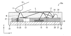
- FIG. 1 is a schematic sectional view of an optical pointing device 30 according to the first embodiment.
- the optical pointing device 30 includes a substrate portion 26 and a cover portion (light guide) 24.
- the board portion 26 includes a circuit board 21, a light source 16, an image sensor 15, and transparent resins 20 and 20 ′.
- the transparent resin 20 includes a lens portion 27.
- the cover portion 24 includes a contact surface (incident portion) 11, a bending element (reflecting portion) 12 that forms an inclined surface (inclined surface) 13, an imaging element (imaging reflecting portion) 14, and reflecting surfaces (reflecting films) 17 and 18. including.
- the subject 10 that is in contact with the contact surface 11 of the cover unit 24 is a subject such as a fingertip, and is an object for which the optical pointing device 30 detects movement.
- the optical pointing device 30 is described in a small size for convenience.
- the thickness direction (vertical direction in FIG. 1) of the optical pointing device 30 is defined as the Z axis
- the width direction (horizontal direction in FIG. 1) of the optical pointing device 30 is defined as the Y axis.
- the direction from the lower part to the upper part of the optical pointing device 30 is the positive direction of the Z axis
- the direction from the light source 16 to the image sensor 15 is the positive direction of the Y axis (light guide direction).
- the negative direction of the Z axis is also referred to as the vertical direction
- the positive direction of the Y axis is also referred to as the horizontal direction.
- the depth direction of the optical pointing device 30 is the X axis
- the direction from the back side to the near side of the optical pointing device 30 shown in FIG. 1 is the positive direction of the X axis.
- the light source 16 and the image sensor 15 are mounted on one circuit board 21.
- the light source 16 and the image sensor 15 are electrically connected to the circuit board 21 by wire bonding or flip chip mounting.
- a circuit is formed on the circuit board 21.
- the circuit controls the light emission timing of the light source 16 or receives an electrical signal output from the image sensor 15 to detect the movement of the subject.
- the circuit board 21 has a planar shape made of the same material, and is made of, for example, a printed board or a lead frame.
- the light source 16 emits light toward the contact surface 11 of the cover portion 24.
- the light M emitted from the light source 16 is refracted by the bending element 12 of the cover portion 24 via the lens portion 27 of the transparent resin 20 and the traveling direction is changed to reach the contact surface 11. That is, the light M enters the contact surface from an oblique direction (at a certain incident angle with respect to the contact surface).
- the cover portion 24 is made of a material having a refractive index larger than that of air, the light M that has reached the contact surface 11 partly touches the contact surface 11 when the subject 10 does not exist on the contact surface 11. The light is transmitted and the remaining part is reflected by the contact surface 11.
- the light source 16 is realized by a light source such as an LED, for example, and is preferably realized by an infrared light emitting diode with high brightness.
- the image sensor 15 emits the light reflected by the subject 10 irradiated by the light source 16 (L1 to L3 (hereinafter collectively referred to as the light L1 to L3).
- the image on the contact surface 11 is formed based on the received light and converted into image data.
- the image sensor 15 is an image sensor such as a CMOS or a CCD.
- the image sensor 15 includes a DSP (Digital Signal Processor: calculation unit) (not shown), and captures received light as image data in the DSP.
- the image sensor 15 continues to capture images on the contact surface 11 at regular intervals in accordance with instructions from the circuit board 21.
- the image captured by the image sensor 15 is different from the image captured immediately before.
- the image sensor 15 compares the values of the same portion of the captured image data with the immediately preceding image data, and calculates the movement amount and movement direction of the subject 10. That is, when the subject 10 on the contact surface 11 moves, the captured image data is image data indicating a value deviated from the image data captured immediately before by a predetermined amount.
- the image sensor 15 calculates the movement amount and movement direction of the subject 10 based on the predetermined amount.
- the image sensor 15 outputs the calculated movement amount and movement direction to the circuit board 21 as electric signals.
- the DSP may be included in the circuit board 21 instead of in the image sensor 15. In that case, the image sensor 15 transmits the captured image data to the circuit board 21 in order.
- the image sensor 15 captures an image of the contact surface 11 when the subject 10 is not present on the contact surface 11.
- the image sensor 15 captures an image of the surface of the subject 10 in contact with the contact surface 11.
- the image sensor 15 captures an image of a fingertip fingerprint.
- the DSP of the image sensor 15 since the image data captured by the image sensor 15 is different from the image data when the subject 10 is not on the contact surface 11, the DSP of the image sensor 15 has the subject 10 on the contact surface 11. A signal indicating that is touching is transmitted to the circuit board 21.
- the movement amount and movement direction of the subject 10 are calculated compared with the image data captured immediately before by the DSP, and a signal indicating the calculated movement amount and movement direction is transmitted to the circuit board 21. .
- the light source 16 and the image sensor 15 are sealed with a translucent resin, and transparent resins 20 and 20 'are formed around them.
- the shape of the transparent resins 20 and 20 ' is a substantially rectangular parallelepiped.
- a hemispherical lens portion 27 is formed on the upper surface (top surface) of the transparent resin 20 in the transparent resin 20.
- the lens unit 27 is located above the light source 16 and condenses the light M emitted from the light source 16.
- the bottom surfaces of the transparent resins 20 and 20 ′ are in close contact with and in contact with the upper surface of the circuit board 21, and concave portions that are in close contact with the light source 16 and the image sensor 15 are formed.
- the side surface on the negative side of the Y axis of the transparent resin 20 and the side surface on the positive side of the Y axis of the transparent resin 20 ′ are flush with the side surface of the circuit board 21.
- a thermosetting resin such as silicone resin or epoxy resin or a thermoplastic resin such as ABS (Acrylonitrile Butadiene Styrene) is used.
- the light source 16 and the image sensor 15 mounted on the circuit board 21 are respectively sealed with the light-transmitting resin, the circuit board 21, the light source 16, the image sensor 15, and the transparent resins 20 and 20 ′. Is formed as a single unit. Therefore, the number of parts of the optical pointing device 30 can be reduced, and the number of assembly processes can also be reduced. Accordingly, the manufacturing cost of the optical pointing device 30 can be reduced, and the optical pointing device 30 with high subject detection accuracy can be realized.
- the light source 16 and the image sensor 15 are individually sealed with transparent resins 20 and 20 '. Therefore, it is possible to prevent the light M emitted from the light source 16 from propagating through the transparent resin and leaking into the image sensor 15. In other words, since stray light is prevented from entering the image sensor 15, it is possible to prevent malfunction of the optical pointing device 30 due to stray light and to detect the subject 10 with high accuracy.
- the cover part 24 protects each part and each element constituting the optical pointing device 30 such as the light source 16 and the imaging element 15.
- the cover part 24 is located on the upper side of the substrate part 26 and is in close contact with the side surface and the upper surface of the substrate part 26.
- the surface of the cover 24 that is on the negative side of the Z-axis and that is not exposed to the outside when mounted on the substrate 26 and formed as the optical pointing device 30 is referred to as the back of the cover 24.
- the surface of the cover 18 that faces the substrate portion 26 is the back surface. That is, a part of the back surface of the cover portion 24 is in close contact with and in contact with the side surface and the upper surface of the substrate portion 26.
- the bottom surface 25 of the cover part 24 forms the same plane as the bottom surface of the substrate part 26.
- the upper surface of the cover portion 24 is parallel to the bottom surface 25 of the cover portion 24 and the bottom surface of the substrate portion 26, and both side surfaces of the cover portion 24 are the upper surface of the cover portion 24, and the bottom surface 25 of the cover portion 24 and the substrate portion.
- a surface perpendicular to the bottom surface of 26 is formed. That is, the optical pointing device 30 has a substantially rectangular parallelepiped shape. However, the shape is not limited to this, and it is sufficient that the upper surface of the cover portion 24 is parallel to the bottom surface 25 of the cover portion 24 and the bottom surface of the substrate portion 26, and both side surfaces of the cover portion 24 are the upper surface of the cover portion 24.
- a surface perpendicular to the bottom surface 25 of the cover portion 24 and the bottom surface of the substrate portion 26 may not be formed.
- the shape of the optical pointing device 30 may be trapezoidal. That is, if the side surface of the cover unit 24 is flat, the total length of the upper surface of the cover unit 24 (the top surface of the optical pointing device 30) and the bottom surface 25 of the cover unit 24 and the bottom surface of the substrate unit 26 ( (The length of the bottom surface of the optical pointing device 30) may be different.
- the contact surface 11 is a surface where the subject 10 is in contact with the optical pointing device 30.
- the contact surface 11 is an upper surface of the cover portion 24 and is located above the light source 16.
- the bending element (prism) 12 constitutes a part of the cover portion 24, is located above the light source 16 and below the contact surface 11, and is on a portion that does not contact the substrate portion 26 on the back surface of the cover portion 24. It is formed in a recessed portion on the back surface of the cover portion 24 located.
- the bending element 12 is formed with an inclined surface 13, and a narrow angle formed by the inclined surface 13 and the upper surface of the cover portion 24 is defined as an inclination angle ⁇ .
- the bending element 12 refracts the light M emitted from the light source 16 on the inclined surface 13 and converts the path of the light M so as to go to the subject 10.
- the bending element 12 totally reflects the light L reflected from the subject 10 by the inclined surface 13, and converts the path of the light L in the positive direction of the Y axis inside the cover portion 24. .
- the bending element 12 reflects the light reflected from the subject 10 and incident on the inside of the cover portion 24 from the contact surface 11 so as to guide the light in the horizontal direction.
- the light L reflected from the subject 10 that has been totally reflected by the inclined surface 13 is directed to a reflection surface 17 described later.
- the inclined surface 13 of the bending element 12 transmits the light M and totally reflects the light L.
- the cover portion 24 may be made of an air layer using a visible light absorption type polycarbonate resin or acrylic resin having a refractive index of about 1.5. That is, an aluminum reflective film or the like is not deposited on the inclined surface 13 of the bending element 12 in order to totally reflect the light L.
- the imaging element (lens) 14 reflects the reflected light L from the subject 10 and forms an image of the subject 10 on the imaging element 15. Specifically, the light reflected in the horizontal direction by the bending element 12 is reflected in the opposite direction to the horizontal direction (the negative direction of the Y axis) and imaged. The light imaged by the imaging element 14 exits the cover portion 24 and enters the imaging element 15.
- a portion where the light imaged by the imaging element 14 is emitted toward the imaging element 15 is referred to as an emission portion.
- the emission part is a part of the back surface of the cover part 24.
- the imaging element 14 constitutes a part of the cover part 24, is located above the image sensor 15 and on the positive side of the Y axis from the image sensor 15, and the substrate part 26 on the back surface of the cover part 24 It is formed in a recess on the back surface of the cover portion 24 located at a portion that does not contact.
- the imaging element 14 is formed with a toroidal surface having different curvatures in two orthogonal directions.
- the imaging element 14 reflects the reflected light L so as to form an image on the imaging element 15 by the toroidal surface.
- a reflective film of metal for example, aluminum, nickel, gold, silver, dielectric dichroic film, etc.
- the reflecting surface 17 reflects the light L so that the light L totally reflected by the inclined surface 13 is incident on the imaging element 14 and the light L reflected from the imaging element 14 is incident on the imaging element 15. It is.
- the reflection surface 17 is located above the image sensor 15 and on the upper surface of the cover portion 24.
- the reflection surface 17 is formed by depositing a reflection film on the upper surface of the cover portion 24. Since the reflective film forming the reflective surface 17 is exposed to the outside and can be seen well by the user, it is desirable to make the film as inconspicuous as possible in appearance.
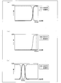
- FIG. 2A is a diagram showing the transmittance and reflectance at each wavelength, where the horizontal axis represents wavelength (nm) and the vertical axis represents transmittance and reflectance (%).
- the dotted line in the figure indicates the transmittance, and the solid line indicates the reflectance (hereinafter, the same applies to (b) and (c) in FIG. 2).
- the reflecting film forming the reflecting surface 17 reflects infrared light having a wavelength band of 800 nm or more irradiated from the light source 16 and transmits light having a visible wavelength band of 800 nm or less. That's fine.
- the reflected light L from the subject 10 is efficiently reflected by appropriately setting the wavelength of the light emitted from the light source 16 and the reflectance and transmittance characteristics of the reflecting film forming the reflecting surface 17.
- the reflective surface 17 which is not conspicuous in appearance can be formed.
- the cover portion 24 may be formed of a material having the characteristics shown in FIG. preferable. Specifically, the material of the cover portion 24 may be a visible light absorption type polycarbonate resin or acrylic resin that transmits only infrared light.
- the cover part 24 By forming the cover part 24 with such a material, visible light components can be blocked by the cover part 24 from unnecessary light entering from the outside of the cover part 24.
- the reflection surface 17 that reflects infrared light
- the infrared light component of the unnecessary light can be blocked by the reflection surface 17. By blocking unnecessary light incident on the optical pointing device 30, malfunction due to the unnecessary light can be prevented.
- the surface of the cover unit 24, which is the surface of the optical pointing device 30, for example, a predetermined surface as shown in FIG. It is only necessary to coat with a material that reflects only the wavelength band of green (green in the illustrated example) and transmits other wavelengths.
- a material having such characteristics By coating the upper surface of the cover portion 24 and the upper surface of the reflecting surface 17 with a material having such characteristics, a desired color is applied to the surface of the optical pointing device 30 without impairing the optical characteristics of the optical pointing device 30. Can be attached.
- the reflection surface 18 reflects the light L reflected from the imaging element 14 and reflected by the reflection surface 17 toward the reflection surface 17 again.
- the reflection surface 18 is located above the image sensor 15 and on the positive side of the Y axis from the image sensor 15, and is located on the back surface of the cover portion 24.
- the reflection surface 18 is formed by depositing a reflection film on the back surface of the cover portion 24.
- the reflective film forming the reflective surface 18 is preferably one that efficiently reflects light.
- the reflecting surface 18 is formed by vapor-depositing a metal such as aluminum, nickel, gold, silver, or a dielectric dichroic film.
- the path through which the light emitted from the light source 16 reflects the subject 10 and enters the image sensor 15 will be described again.
- the light M emitted from the light source 16 is refracted and transmitted by the inclined surface 13 of the bending element 12 and reaches the contact surface 11.
- the light M emitted from the light source 16 is scattered and reflected on the surface of the subject 10 in contact with the contact surface 11.
- the light L reflected by the surface of the subject 10 is totally reflected by the inclined surface 13 of the bending element 12, and the path changes in the positive direction of the Y axis.
- the light L totally reflected by the inclined surface 13 is reflected by the reflecting surface 17 and reaches the imaging element 14.
- the light L is reflected back by the imaging element 14, is reflected one after another by the reflecting surface 17, the reflecting surface 18, and the reflecting surface 17 and enters the imaging device 15.
- the light incident on the center of the image sensor 15 (reflected by the subject 10 located at the center of the contact surface 11).
- Light is L2
- light incident on the positive end of the Y axis of the image sensor 15 (light reflected by the subject 10 located at the negative end of the Y axis of the contact surface 11) is L1.
- the light incident on the negative end of the Y axis of the image sensor 15 (the light reflected by the subject 10 located at the positive end of the Y axis of the contact surface 11) is L3.
- the imaging element 14 that reflects the light L and forms an image on the imaging element 15
- a difference in optical path lengths until the lights L 1, L 2, and L 3 reach the imaging element 15 is reduced. be able to.
- FIG. 3 is a diagram schematically showing the positional relationship among the contact surface 11, the imaging element 14 (or the imaging element 14 a), and the imaging element 15.
- FIG. 3 shows the optical paths of the lights L1, L2, and L3 when the center axis of the contact surface 11 is shifted from the center axis of the imaging element 14 (or imaging element 14a).
- 3A shows a case where the imaging element 14 which is a reflective lens that reflects the light L is used as in the present embodiment
- FIG. 3B shows a transmission that transmits the light L. It is a figure which shows the case where the imaging element 14a which is a mold lens is used.
- the imaging element 14 is tilted with respect to the central axis of the contact surface 11 (perpendicular line passing through the center of the contact surface 11) and not inclined in parallel. Even in the case of arrangement, the difference in the optical path length from the contact surface 11 to the surface of the image sensor 15 in each light L1, L2, and L3 is reduced while setting the surface of the image sensor 15 parallel to the contact surface 11. be able to.
- a transmissive lens as shown in FIG. 3B, when the lens central axis of the imaging element 14a is tilted with respect to the central axis of the contact surface 11, the light L1, L2, and L3 contact each other.
- the contact surface 11 and the surface of the image sensor 15 need to be arranged not in parallel but crossing each other. Therefore, in the case of a transmissive lens, it is difficult to reduce the thickness of the optical pointing device 30. That is, when the imaging element 14 is arranged with the lens central axis inclined from the central axis of the contact surface 11, the reflection type lens is used as the imaging element 14 rather than the transmission type lens while reducing the optical path length difference. It is easy to make the optical pointing device 30 thinner.
- the contact surface 11, the bending element 12, and the imaging element 14 are formed integrally with the cover portion 24. Therefore, the number of parts of the optical pointing device 30 can be reduced, and the number of assembly processes can also be reduced. Further, by forming a mold for forming the cover portion 24 with high accuracy, the inclined surface 13 and the imaging element 14 of the bending element 12 can be manufactured with high accuracy, and the contact surface 11 and the bending element 12 are manufactured. Further, the positional relationship of the imaging element 14 can be arranged with high accuracy without variation. Accordingly, the manufacturing cost of the optical pointing device 30 can be reduced, and the optical pointing device 30 with high subject detection accuracy can be realized.
- the contact surface, bending element, imaging element, etc. are separate parts.When these parts are assembled, shapes such as the assembly surface and fitting shape are formed at the joints between the parts. There was a need to form. In addition, it is necessary to secure a spatial margin for adjusting the relative positional relationship between the components. However, when the contact surface 11, the bending element 12, and the imaging element 14 are formed integrally with the cover portion 24 as in the present application, it is not necessary to form the above shape, and if there is a minimum optical surface. It is not necessary to secure a spatial margin for adjusting the position.
- the thickness of the cover part 24 including the contact surface 11, the bending element 12 and the imaging element 14 can be reduced. it can. Therefore, the thickness of the optical pointing device 30 can be reduced.
- the cover portion 24 is assembled above the substrate portion 26 using the side surface and the upper surface of the substrate portion 26 as a reference for positioning the cover portion 24. Therefore, the positional relationship between the substrate part 26 and the cover part 24 can be arranged with high accuracy. Therefore, since each part and each element constituting the optical pointing device 30 can be arranged with high accuracy, the optical pointing device 30 with high detection accuracy of the subject 10 can be realized.
- the path of the light L (until it enters the transparent resin 20 ′ that is reflected by the subject 10 and covers the image sensor 15) is contained in the cover portion 24 that is one member. That is, the light L propagates through one medium (light guide). Specifically, there is one process from the incident of the reflected light L from the subject 10 to the cover 24 until total reflection in the horizontal direction by the bending element 12, reflection by the imaging element 14, and emission to the imaging element 15. This is performed in the cover 24 that is a medium. Therefore, since scattering reflection and attenuation occurring at the boundary between different media can be prevented, the imaging element 15 can capture a clear image. Therefore, the optical pointing device 30 can stably detect the subject 10 with high accuracy.
- a light shielding resin may be resin-sealed on the side surface of the transparent resin 20 and the upper surface excluding the lens portion. Further, a light-shielding resin may be resin-sealed on the side surface of the transparent resin 20 ′ and on the upper surface of the transparent resin 20 ′ excluding a portion where the reflected light L from the subject is transmitted.
- a thermosetting resin such as a silicone resin or an epoxy resin or a thermoplastic resin such as ABS is used in the same manner as the light-transmitting resin.
- the light-blocking resin includes carbon black.
- the light emitted from the light source 16 is reflected directly or at a place other than the subject 10 and is reflected on the image sensor 15.
- the incident can be prevented. It is possible to prevent so-called stray light that is not reflected light L from the subject 10 from entering the image sensor 15. Therefore, malfunction of the optical pointing device 30 due to stray light can be prevented, and the subject 10 can be detected with high accuracy.
- the upper surface of the transparent resin 20 ′ excluding the portion through which the reflected light L is transmitted may be blackened or roughened into a ground glass shape.
- the cover portion 24 is assembled above the substrate portion 26 with reference to the surface formed of the light-shielding resin and both side surfaces of the circuit board 21.
- the inclination angle ⁇ formed by the inclined surface of the bending element was set to 24 degrees. Further, the length z2 on the Z axis from the back surface of the cover portion in contact with the upper surface of the substrate portion to the upper surface of the cover portion was set to 0.5 mm. This length z2 is referred to as the thickness of the cover portion.
- the length y2 on the Y axis from the center of the contact surface to the center of the toroidal surface of the imaging element 14 is 2.8 mm, and the length y1 on the Y axis from the center of the contact surface to the center of the image sensor is 1. It was 4 mm.
- the length z1 on the Z axis from the upper surface of the cover part to the center of the toroidal surface of the imaging element is 0.38 mm, and the length on the Z axis from the upper surface of the cover part to the upper surface of the image sensor z3 was 0.62 mm.
- the XY cross section of the toroidal surface of the imaging element is a spherical surface having a radius of curvature of -2.5644773 mm, the YZ cross section is an aspherical shape, and the aspherical shape is designed by the following aspherical expression (Formula 1).
- K is a conic constant
- R is a radius of curvature
- A, B, C, and D are second-order, fourth-order, sixth-order, and eighth-order aspheric coefficients
- Z is a height Y from the optical axis. The length of a perpendicular line drawn from a point on the aspheric surface at the position to the tangent plane (plane perpendicular to the optical axis) of the apex of the aspheric surface is shown.
- FIG. 4 is a schematic sectional view of an optical pointing device 30a according to the second embodiment.
- a diffractive element 12 ′ is arranged instead of the bending element 12 that totally reflects the reflected light L in the horizontal direction in the first embodiment.
- differences from the first embodiment due to the arrangement of the diffraction element 12 ′ in the second embodiment will be described.
- the description of the same configuration as in the first embodiment is omitted.
- the transparent resin 20 is such that the negative side surface of the Y axis is not flush with the side surface of the circuit board 21, and the negative side surface of the Y axis is from the side surface of the circuit board 21. Located on the positive side of the Y-axis.
- the light M emitted from the light source 16 is transmitted and refracted on the back surface of the cover portion 24 via the lens portion 27 of the transparent resin 20 and reaches the contact surface 11.
- the cover part 24 includes the contact surface 11, the diffraction element 12 ′, the imaging element 14, and the reflection surfaces 17 and 18.
- the cover part 24 is located above the board part 26, and both side surfaces of the circuit board 21, the negative side surface of the transparent resin 20 on the Y axis side, and the positive side surface and upper surface of the transparent resin 20 'on the Y axis side. Is in close contact with.
- the diffractive element 12 ′ is located above the light source 16 and below the contact surface 11 and in a portion that does not contact the substrate portion 26 on the back surface of the cover portion 24.
- the diffractive element 12 ′ reflects the light L reflected from the subject 10, and converts the path of the light L in the positive direction of the Y axis inside the cover portion 24.
- the light L reflected from the subject 10 and reflected by the diffraction element 12 ′ travels toward the reflecting surface 17.
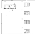
- FIG. 5A is a schematic configuration diagram showing a cross-sectional shape of the diffraction element 12 ′.
- the diffractive element 12 ' is a reflective diffractive element that uses + 1st order reflected diffracted light.
- the cross-sectional shape as shown in FIG. 5A is preferably a blaze shape so that + 1st order light is strongly generated.
- the light use efficiency can be improved, and the 0th order light, the ⁇ 1st order light and the higher order diffracted light that become stray light can be suppressed. Therefore, in the optical pointing device 30a, it is possible to prevent the imaging performance of the optical system from deteriorating.
- a reflective film al for example, aluminum, silver, gold, dielectric dichroic film, etc.
- a reflective film al is vapor-deposited on the outer surface (surface on the negative side of the Z axis) of the diffraction element 12 ′. It is desirable.
- the depth of the blazed groove (the length in the Z direction) of the diffractive element 12 ' is t.
- the groove depth t is desirably a depth that maximizes the + 1st order diffraction efficiency.
- the blazed groove pattern of the diffractive element 12 ' has a straight equal pitch as shown in FIG. 5B, and it is desirable to make it as fine as possible in order to maximize the diffraction angle.
- the groove pattern of the diffractive element 12 ′ is curved as shown in FIG. Can be corrected.
- the groove pitch of the diffractive element 12 ′ is not an equal pitch but a pattern in which the pitch gradually changes, and the diffractive element 12 ′ is provided so as to have a lens effect in a certain direction. You may design. In this case, it is possible to correct aberration that occurs due to the difference in focal length between the X-axis direction and the Y-axis direction on the image sensor 15.
- both the distortion of the image and astigmatism can be corrected by making the groove pattern of the diffractive element 12 ′ into a curved and unequal pitch pattern. it can.
- a reflective Fresnel lens may be used for the diffractive element 12'.
- a specific shape of the Fresnel lens is shown in FIG.
- FIG. 6 is a schematic configuration diagram showing a cross-sectional shape of a diffraction element 12 ′ that is a Fresnel lens, as in FIG.
- the cross-sectional shape of the Fresnel lens is a blaze shape.
- a reflective film al for example, aluminum, silver, gold, dielectric dichroic film, etc.
- the thickness of the cover portion 24 can be made uniform compared to the case where a prism or a bulk lens is formed on a part of the cover portion 24. Therefore, it is possible to reduce the thickness of the optical pointing device 30a while increasing the strength of the cover portion 24.
- a hologram lens is used for the diffraction element 12 ′, aberrations that cannot be corrected by a normal lens can be corrected, so that the imaging performance is improved, and the image of the subject 10 is projected clearly on the imaging element 15. Can do.
- the diffractive element 12 ′ when used to reflect the light L reflected from the subject 10 in the horizontal direction, compared with the case where the bending element (prism) 12 is formed in the cover part 24, The thickness can be made uniform. Therefore, it is possible to reduce the thickness while increasing the strength of the cover portion 24.
- the light irradiated from the light source 16 can be irradiated to the contact surface 11 with uniform light intensity.
- the size of the bending element 12, particularly the length in the Z-axis direction is optical pointing. This greatly affects the thickness of the device. That is, in order to design the optical pointing device thin, it is important to reduce the length of the bending element 12 in the Z-axis direction.
- the size of the bending element 12 cannot be designed freely, and the size of the bending element 12 depends on the size of the contact surface 11.
- the contact surface 11 in order to detect the pattern on the contact surface 11, the contact surface 11 must have a certain amount of area. Therefore, if the area of the contact surface 11 is to be secured, the bending element 12 inevitably increases, and the thickness of the optical pointing device 30 (size in the Z-axis direction) cannot be reduced.
- the optical pointing device 30a is made thinner than the first embodiment by using a diffractive element 12 'that can be smaller in length in the Z-axis direction than the bending element 12 instead of the bending element 12. Can be achieved.
- the circuit board 21, the side surface on the negative side of the Y axis of the transparent resin 20, and the side surface on the positive side of the Y axis of the transparent resin 20 ′ and the upper surface are used as a reference.
- the cover part 24 is assembled above the part 26. Therefore, the positional relationship between the substrate part 26 and the cover part 24 can be arranged with high accuracy. Therefore, since each part and each element constituting the optical pointing device 30a can be arranged with high accuracy, the optical pointing device 30a with high detection accuracy of the subject 10 can be realized.
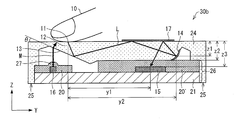
- FIG. 7 is a schematic sectional view of an optical pointing device 30b according to the third embodiment.
- the reflective surface 18 with which the cover part 24 is provided in 1st Embodiment is removed. That is, in the third embodiment, the cover portion 24 includes the contact surface 11, the bending element 12, the imaging element 14, and the reflection surface 17.
- the description of the same configuration as that of the first embodiment is omitted.
- the path of the light L in the first embodiment differs due to the absence of the reflecting surface 18. That is, in the third embodiment, the reflected light L from the subject 10 is totally reflected in the horizontal direction by the inclined surface 13 of the bending element 12 and travels toward the reflecting surface 17. Then, the light L is reflected by the reflecting surface 17 and reaches the imaging element 14. The light L is folded back and reflected by the imaging element 14, further reflected by the reflecting surface 17, and incident on the imaging element 15.
- the light L reflected by the imaging element 14 is reflected by the reflecting surface 17 only once before entering the imaging element 15. Therefore, until the reflected light L from the subject 10 enters the image sensor 15, the chance of reflectance loss when reflected by each element is reduced, and the light utilization efficiency is increased. Further, since the optical path length of the light L can be designed to be relatively short, there is an effect that a bright optical system with a small F number can be realized.
- the reflecting surface 18 is removed from the first embodiment.
- the reflecting surface 18 is similarly applied to the second embodiment. It is also possible to remove it. In this case, it can be realized by appropriately designing the shape and position of the diffraction element 12 ′ and the positions of the imaging element 14 and the imaging element 15.
- the optical pointing device according to the third embodiment Next, an example of the optical pointing device according to the third embodiment will be described together with specific settings and numerical values.
- a visible light absorption type polycarbonate resin having a refractive index of 1.59 was used as the material of the cover portion.
- the inclination angle ⁇ formed by the inclined surface of the bending element was set to 25 degrees.
- the length z2 on the Z axis from the back surface of the cover portion in contact with the upper surface of the substrate portion to the upper surface of the cover portion was set to 0.54 mm.
- the length y2 on the Y axis from the center of the contact surface to the center of the toroidal surface of the imaging element 14 is 2.75 mm, and the length y1 on the Y axis from the center of the contact surface to the center of the image sensor is 2. It was 1 mm.
- the length z1 on the Z axis from the upper surface of the cover part to the center of the toroidal surface of the imaging element is 0.43 mm, and the length on the Z axis from the upper surface of the cover part to the upper surface of the image sensor z3 was 0.60 mm.
- the XY cross section of the toroidal surface of the imaging element is a spherical surface with a radius of curvature of -0.4193264 mm
- the YZ cross section is an aspherical shape
- the aspherical shape is designed by the following aspherical formula (Formula 2).
- K is a conic constant
- R is a radius of curvature
- A, B, C, D, E, F, and G are second order, fourth order, sixth order, eighth order, tenth order, and twelfth order, respectively.
- the 14th aspheric coefficient, Z is the length of a perpendicular drawn from a point on the aspheric surface at a height Y from the optical axis to the tangential plane (plane perpendicular to the optical axis) of the apex of the aspheric surface Indicates.
- FIG. 8 is a schematic sectional view of an optical pointing device 30c according to the fourth embodiment.
- the imaging element 14 ′ is formed by changing the shape and arrangement of the imaging element 14 of the cover portion 24 in the first embodiment.
- differences from the first embodiment by changing the imaging element 14 to the imaging element 14 ′ in the fourth embodiment will be described.
- the description of the same configuration as that of the first embodiment is omitted.
- the cover portion 24 includes a contact surface 11, a bending element 12, an imaging element 14 ', and reflecting surfaces 17 and 18'. Unlike the first embodiment, the entire upper surface of the transparent resin 20 ′ and the back surface of the cover part 24 are in close contact with each other, and the cover part 24 is located above the transparent resin 20 ′ (the image pickup device 15). No recess is formed on the back surface of the plate.
- the imaging element 14 ′ reflects the reflected light L from the subject 10 and forms an image of the subject 10 on the imaging element 15.
- the imaging element 14 ′ is located above the image sensor 15 and on the positive side of the Y axis from the image sensor 15, and is located at the corner between the upper surface and the side surface of the cover portion 24.
- the imaging element 14 ' forms a curved surface. That is, the corner between the upper surface and the side surface of the cover portion 24 on the positive direction side of the Y axis is R-processed.
- a reflective film of metal for example, aluminum, nickel, gold, silver, dielectric dichroic film, etc.
- Evaporate for example, aluminum, nickel, gold, silver, dielectric dichroic film, etc.
- the reflection surface 17 reflects the light L totally reflected by the inclined surface 13 toward the reflection surface 18 ′, and images the light L reflected from the imaging element 14 ′ and reflected by the reflection surface 18 ′.
- the light L is reflected so as to enter the element 15.
- the reflection surface 17 is located above the image sensor 15 and on the upper surface of the cover portion 24.
- the reflection surface 17 is formed by depositing a reflection film on the upper surface of the cover portion 24. Since the reflective film forming the reflective surface 17 is exposed to the outside and can be seen well by the user, it is desirable to make the film as inconspicuous as possible in appearance.
- the reflecting surface 18 ′ reflects the reflected light L from the subject 10 reflected by the reflecting surface 17 toward the imaging element 14 ′, and reflects the light L reflected from the imaging element 14 ′. It reflects toward the 17.
- the reflective surface 18 ′ is located above the image sensor 15 and on the positive side of the Y axis from the image sensor 15, and is located on the back surface of the cover portion 24.
- the negative end of the reflecting surface 18 ′ on the Y axis may be above the positive end of the Y axis of the image sensor 15.
- the reflection surface 18 ′ is formed by depositing a reflection film on the back surface of the cover portion 24.
- the reflective film forming the reflective surface 18 ' is preferably one that reflects light efficiently.
- the reflective surface 18 ′ is formed by depositing a metal such as aluminum, nickel, gold, silver, or a dielectric dichroic film.
- the light L reflected by the surface of the subject 10 is totally reflected by the inclined surface 13 of the bending element 12, and the path changes in the positive direction of the Y axis.
- the light L totally reflected by the inclined surface 13 is reflected by the reflecting surface 17 and the reflecting surface 18 ′ and reaches the imaging element 14 ′. Then, the light L is reflected back by the imaging element 14 ′, reflected one after another by the reflecting surface 18 ′ and the reflecting surface 17, and enters the image sensor 15.
- the imaging element 14 ′ is not formed on the back surface of the cover portion 24, but the upper surface and side surfaces of the cover portion 24 on the positive side of the Y axis. And formed at the corner. Therefore, it is not necessary to make a shape in which the back surface of the cover portion 24 is greatly dug, and the cover portion 24 can be easily manufactured by molding. Furthermore, since it is not necessary to form a recess in the back surface of the cover part 24 located above the image sensor 15, the thickness of the cover part 24 can be made uniform. Therefore, it is possible to reduce the thickness of the optical pointing device 30c while increasing the strength of the cover portion 24.
- the cover portion 24 is assembled above the substrate portion 26 with reference to the side surface and the upper surface of the substrate portion 26. Therefore, the positional relationship between the substrate part 26 and the cover part 24 can be arranged with high accuracy. Therefore, since each part and each element constituting the optical pointing device 30c can be arranged with high accuracy, the optical pointing device 30c with high detection accuracy of the subject 10 can be realized.
- FIG. 9 is a diagram illustrating an appearance of the mobile phone 100 on which the optical pointing device 107 is mounted.
- 9A is a front view of the mobile phone 100
- FIG. 9B is a rear view of the mobile phone 100
- FIG. 9C is a side view of the mobile phone 100.
- FIG. 9 shows an example in which the electronic device is a mobile phone, the present invention is not limited to this.
- the electronic device may be, for example, a PC (particularly a mobile PC), a PDA, a game machine, a remote controller such as a television, or the like.
- the mobile phone 100 includes a monitor-side casing 101 and an operation-side casing 102.
- the monitor-side casing 101 includes a monitor unit 105 and a speaker unit 106
- the operation-side casing 102 includes a microphone unit 103, a numeric keypad 104, and an optical pointing device 107.
- Any of the optical pointing devices 30, 30a, 30b, and 30c described in the first to fourth embodiments can be applied to the optical pointing device 107 mounted on the mobile phone 100.
- the optical pointing device 107 is arranged on the upper part of the numeric keypad 104.
- the arrangement method and the direction of the optical pointing device 107 are described here. It is not limited.
- the speaker unit 106 outputs audio information to the outside, and the microphone unit 103 inputs audio information to the mobile phone 100.
- the monitor unit 105 outputs video information. In the present embodiment, the monitor unit 105 displays input information from the optical pointing device 107.
- the cellular phone 100 of this embodiment includes an upper casing (monitor-side casing 101) and a lower casing (operation-side casing 102).
- a so-called foldable mobile phone 100 is connected through a hinge. Since the folding type is the mainstream of the cellular phone 100, the folding type cellular phone is given as an example in the present embodiment, and the cellular phone 100 on which the optical pointing device 107 can be mounted is foldable. It is not limited.
- the optical pointing device of the present invention that can be thinned as described above is a preferred invention for an electronic device that needs to be thinned, such as the cellular phone 100.
- the light guide according to the present invention reflects the light incident from the incident portion to guide the light incident in the light guide direction, and further reflects the reflected light with respect to the light guide direction. And an imaging reflection part that forms an image while reflecting in the opposite direction, and the light imaged by the imaging reflection part is emitted from the emission part.
- the light guide method according to the present invention reflects the light incident from the incident portion to guide the light in the light guide direction, further reflects the reflected light in the opposite direction to the light guide direction, and forms an image. Then, the reflected and imaged light is emitted from the emission part.
- the light guide since the light guide includes the reflection portion and the imaging reflection portion, the light guide, the reflection portion, and the imaging reflection portion can be configured by one component. Therefore, it is possible to reduce the number of parts constituting the optical pointing device including the light guide. Therefore, the number of assembling steps can be reduced in the manufacturing process of the optical pointing device. Therefore, it is possible to suppress an assembly error that occurs when assembling each component.
- the reflecting portion and the imaging reflecting portion can be manufactured with high accuracy, and the positions of the incident portion, the reflecting portion, and the imaging reflecting portion can be manufactured. The relationship can be arranged with high accuracy without variation. Therefore, it is possible to reduce the manufacturing cost of the optical pointing device including the light guide and to realize an optical pointing device with high subject detection accuracy.
- an optical pointing device receives a light source that irradiates a subject and reflected light from the subject from an incident portion, guides the incident light, and exits from an exit portion.
- An optical pointing device that includes a light guide that performs an operation and an image sensor that receives light emitted from the light guide, and the light guide guides light incident from the incident portion in a light guide direction. The reflected light is reflected as much as possible, and the reflected light is further reflected and imaged in the opposite direction to the light guide direction, and the reflected and imaged light is emitted from the emitting portion.
- the said light guide reflects in order to guide the light which injected from the said incident part to the light guide direction, and further reflects this reflected light in the opposite direction with respect to the said light guide direction. Then, the light is imaged together, and the reflected and imaged light is emitted from the emission part. That is, apart from the light guide, there is no need to provide a component that reflects to guide light in the light guide direction or a component that reflects in the opposite direction to the light guide direction and forms an image. For this reason, the number of parts constituting the optical pointing device can be reduced. Therefore, the number of assembling steps can be reduced in the manufacturing process of the optical pointing device. Therefore, it is possible to suppress an assembly error that occurs when assembling each component. Therefore, it is possible to reduce the manufacturing cost of the optical pointing device and to realize an optical pointing device with high subject detection accuracy.
- the light guide is preferably formed integrally with a cover portion for protecting the imaging element.
- the cover portion and the light guide are integrally formed, the number of components constituting the optical pointing device can be reduced. Therefore, the number of assembling steps can be reduced in the manufacturing process of the optical pointing device. Therefore, it is possible to suppress an assembly error that occurs when assembling each component.
- the light guide can be manufactured with high accuracy by forming the mold for forming the cover portion with high accuracy. Therefore, the manufacturing cost of the optical pointing device can be reduced, and an optical pointing device with high object detection accuracy can be realized.
- the light source and the imaging device are arranged on a substrate and each is sealed with a transparent resin.
- the light source, the imaging element, and the substrate are integrally formed. For this reason, the number of parts constituting the optical pointing device can be reduced. Therefore, the number of assembling steps can be reduced in the manufacturing process of the optical pointing device. Therefore, it is possible to suppress an assembly error that occurs when assembling each component. Therefore, the manufacturing cost of the optical pointing device can be reduced, and an optical pointing device with high object detection accuracy can be realized.
- the transparent resin in which the light source and the imaging element are respectively resin-sealed has a substantially rectangular parallelepiped shape
- one side surface of the transparent resin in which the light source is resin-sealed is:
- One side surface of the other transparent resin disposed on the same plane as the one side surface of the substrate and resin-sealing the imaging element is disposed on the same plane as the other side surface of the substrate,
- Using the upper surface, both side surfaces of the substrate, and one side surface of the transparent resin in which the light source and the imaging element that are coplanar with the resin are sealed as a reference for positioning the light guide, It is preferable to arrange on the upper side of the substrate.
- a concave portion is formed on the back surface of the light guide with the emitting portion, and the reflecting portion has a slope formed in the concave portion. Is preferred.
- the reflecting portion is a concave portion having an inclined surface located on the back surface where the emitting portion of the light guide is located. Therefore, since the shape of the mold for forming the light guide becomes simple, the light guide can be easily manufactured, and the manufacturing cost of the light guide can be easily reduced.
- the reflection part is formed on a back surface of the light guide with the emission part, and the reflection part is a reflective diffraction element.
- the reflecting portion is a reflective diffractive element located on the back surface of the light guide with the emitting portion. That is, the light guide including the function of the reflection portion can be formed without forming a recess for forming the reflection portion in the light guide. Therefore, the thickness of the light guide can be made more uniform than that of the light guide including the reflective portion of the concave portion, and the light guide can be thinned while increasing the strength of the light guide.
- a concave portion is formed on the back surface of the light guide with the emitting portion, and the imaging reflection portion is formed in the concave portion in the light guide direction. It is preferable to have a toroidal surface in which the curvature of the surface and the curvature of the surface orthogonal to the light guide direction are different.
- the imaging reflection portion has a toroidal surface formed in a concave portion on the back surface where the emission portion of the light guide is located. Therefore, it is possible to satisfactorily correct astigmatism (astigmatism) generated due to a difference in focal length between the light guide direction and the direction orthogonal to the light guide direction. Therefore, the imaging performance of the imaging reflection unit is improved, and the image sensor can clearly capture the image of the subject.
- the reflection part is formed on a back surface of the light guide with the emission part, and the reflection part is a reflection type Fresnel lens.
- the reflection portion is a reflection-type Fresnel lens located on the back surface of the light guide with the emission portion. That is, the light guide including the function of the reflection portion can be formed without forming a recess for forming the reflection portion in the light guide. Therefore, the thickness of the light guide can be made more uniform than that of the light guide including the reflective portion of the concave portion, and the light guide can be thinned while increasing the strength of the light guide.
- the reflection part is formed on a back surface of the light guide with the emission part, and the reflection part is a reflective hologram lens.
- the reflecting portion is a reflective hologram lens. Therefore, it is possible to correct aberrations that cannot be corrected with a normal lens. Accordingly, the imaging performance of the imaging reflection unit that reflects the reflected light of the reflection unit is improved, and the imaging element can clearly capture the image of the subject.
- the light guide according to the present invention further includes a reflection film that totally reflects the light reflected by the reflection portion and emits the light to the imaging reflection portion, and the reflection film includes the light guide having the incident portion. It is preferable that it is a part of the surface of the light body and is located at a place other than the incident part.
- the said reflecting film is a part of surface of the said light guide with the said incident part, is located in places other than the said incident part, and totally reflects the light reflected by the said reflection part Is.
- the surface of the light guide having the incident portion may be in contact with a subject, the subject is in contact with a portion other than the incident portion, and the light reflected by the reflection portion at the location where the subject is in contact
- the light reflected by the reflecting portion is not reflected by the surface of the light guide but by the surface of the subject. Reflecting on the surface of the subject at a place other than the incident portion causes a shift in the path of light reflected by the reflecting portion.
- the imaging performance of the imaging reflection unit is improved, and the image sensor can clearly capture the image of the subject.
- the wavelength of light incident from the incident portion is a non-visible wavelength
- the reflective film transmits light having a visible wavelength
- the reflective film transmits light having a visible wavelength
- the reflective film formed on the surface of the light guide cannot be visually recognized. Therefore, even when a reflective film is formed on the surface of the light guide, the appearance of the light guide is not affected.
- the path of the light incident from the incident part passes through the light guide until the light incident from the incident part is emitted from the output part. It is preferable.
- the path of the light incident from the incident part passes through the light guide until the light incident from the incident part is emitted from the emitting part. That is, the reflected light from the subject passes through the incident part and enters the light guide, then reflects off the reflecting part, reflects off the imaging reflecting part, and exits from the emitting part. In the meantime, the light incident from the incident part propagates in one medium. Therefore, scattering reflection and attenuation occurring at the boundary between different media can be prevented.
- light incident from the incident portion is reflected between a surface of the light guide having the incident portion and a back surface of the light guide having the emitting portion.
- the light is preferably emitted from the emission part.
- the light which injected from the said incident part reflects between the surface of the said light guide with the said incident part, and the back surface of the said light guide with the said output part, and is from the said output part. Exit. For this reason, it is possible to design a long light path from the incidence from the incidence part to the emission from the emission part.
- an electronic apparatus includes the optical pointing device.
- the electronic apparatus includes the optical pointing device that can be easily reduced in thickness.
- the thickness of the optical pointing device greatly affects the thickness of the electronic device. Therefore, even if the optical pointing device is provided, the electronic device can be thinned.
- the present invention can be used for an input device such as a PC or a mobile phone, and can be suitably used for a portable device that is particularly required to be small and thin.
Landscapes
- Physics & Mathematics (AREA)
- Engineering & Computer Science (AREA)
- General Physics & Mathematics (AREA)
- Optics & Photonics (AREA)
- General Engineering & Computer Science (AREA)
- Theoretical Computer Science (AREA)
- Human Computer Interaction (AREA)
- Position Input By Displaying (AREA)
- Image Input (AREA)
- Studio Devices (AREA)
Abstract
光ポインティング装置の部品点数、および、各部品の組み立てまたは貼り付け等の工程数を少なくすることを目的とし、本発明に係る光ポインティング装置(30)に含まれる導光体(24)は、接触面(11)より入射した光を水平方向へ導光すべく反射する折り曲げ素子(12)と、該反射した光をさらに水平方向に対して反対方向に反射するとともに結像する結像素子(14)とを備え、結像素子(14)にて結像した光を出射部より出射する。
Description
本発明は入力装置に関し、より詳細には、携帯電話等の携帯情報端末に搭載可能な光ポインティング装置に関する。
携帯電話やPDA(Personal Digital Assistants)などの携帯情報端末では、一般的に、情報を入力するユーザーインターフェースとしてキーパッドが採用されている。キーパッドは、通常、数字及び文字を入力するための複数個のボタンと方向ボタンとで構成されている。また、近年では携帯情報端末のディスプレイ部にグラフィックなどの表現が可能となることに伴い、ユーザに対する情報の表示方式として、ディスプレイ部を2次元で用いるGUI(Graphical User Interface)が採用されるようになった。
このように携帯情報端末が高機能化し、コンピューターと同等の表示機能を備えることにより、メニューキーおよびその他の機能キーを方向キーとして用いる、従来の携帯情報端末の入力手段では、GUIで表現されたアイコン等の選択には適しておらず、不便であった。そのため、携帯情報端末においても、コンピューターに用いられているマウスやタッチパッドと同様の操作性を有するポインティング装置が求められるようになった。
そこで、携帯情報端末に搭載可能なポインティング装置として、装置に接触する指先等の被写体の模様を撮像素子で観察し、接触面における被写体の模様の変化を抽出することによって、被写体の動きを検知する光ポインティング装置が提案されている。具体的に、光ポインティング装置では、接触面上の被写体に光を照射し、被写体の模様をレンズで撮像素子に結像させ、模様の変化を検出することで被写体の動きを検知している。
光ポインティング装置は、接触面上の被写体から反射された光を撮像素子に結像させるために、接触面から撮像素子までの距離(被写体からの反射光の光路長)をある程度必要とする。そのため、接触面の下部にレンズおよび撮像素子を配置する光ポインティング装置では、接触面に対して垂直方向の長さを短く設計することができなかった。光ポインティング装置の垂直方向の長さは、装置の厚みである。つまり、上述の光ポインティング装置では、装置の薄型化が困難であった。しかしながら、携帯情報端末では、装置の厚みが薄いことが求められるため、光ポインティング装置においてもその厚みである垂直方向の長さを短くすることが求められる。
このような要求を満たすため、接触面の直下にプリズム等の折り曲げ光学素子を配置し、被写体からの反射光を水平方向に折り曲げて撮像素子に結像する光ポインティング装置が提案されている。例えば、特許文献1には、光を垂直経路から水平経路に変換するプリズムと集光レンズと発光手段を備えるホルダーとが組み立てて構成されている光ポインティング装置が開示されている。また、特許文献2には、被写体から反射された光を水平方向に反射する反射鏡と、水平の光経路上に対向して垂直に設置された集光レンズおよびイメージセンサとを備える光ポインティング装置が開示されている。さらに、特許文献3には、が開示されている。
このように、特許文献1~3に記載の光ポインティング装置は、光路を水平方向に折り曲げているため、光路が長くなっても装置の垂直方向の長さ(厚み)には影響しない。このため、光路を長く取りながら垂直方向の長さが短い光ポインティング装置を実現できる。つまり、光ポインティング装置の薄型化が可能となる。
しかしながら、上述のような従来技術は、光ポインティング装置を構成する、外部の衝撃等から保護するカバー部、被写体からの光を水平方向に反射するプリズム(反射鏡)、光を撮像素子に結像(集光)する結像(集光)レンズ部などが複数の部品で構成されているため、光ポインティング装置の製造工程において上記複数の部品の組み立てまたは貼り付け等の工程を要する。組み立てまたは貼り付け等の工程において、各部品の位置ずれによる組立公差が発生する可能性があるため、組み立てまたは貼り付け等の工程数が増加すると、光ポインティング装置の検知精度を高く維持することが困難になる。
また、光ポインティング装置の部品点数が増加すると、光ポインティング装置のコストが高くなるという問題がある。さらに、部品点数が増加することや、各部材において組み立てのための構造が形成されることにより、光ポインティング装置を薄型化することが困難となる。
本発明は、上記の問題点に鑑みてなされたものであり、その目的は、部品点数、および、各部品の組み立てまたは貼り付け等の工程数が少ない、薄型の光ポインティング装置を実現することにある。
本発明に係る導光体は、前記課題を解決するために、入射部より入射した光を導光方向へ導光すべく反射する反射部と、該反射した光をさらに前記導光方向に対して反対方向に反射するとともに結像する結像反射部とを備え、該結像反射部にて結像した光を出射部より出射することを特徴としている。
また、本発明に係る導光方法は、入射部より入射した光を導光方向へ導光すべく反射し、該反射した光をさらに前記導光方向に対して反対方向に反射するとともに結像し、該反射するとともに結像した光を出射部より出射することを特徴としている。
上記の構成によれば、導光体が反射部と結像反射部とを備えているため、導光体と反射部と結像反射部とが1つの部品で構成することができる。よって、導光体を備える光ポインティング装置を構成する部品点数を削減することができる。よって、光ポインティング装置の製造工程において、組立工数を削減することができる。それゆえ、各部品の組み立て時に発生する組立誤差を抑えることができる。また、導光体を成形する金型を高精度で作成することにより、反射部および結像反射部を高精度に製造することができ、且つ、入射部、反射部および結像反射部の位置関係もばらつき無く高精度に配置することができる。従って、前記導光体を備える光ポインティング装置の製造コストを削減することができると共に、被写体の検知精度の高い光ポインティング装置を実現することができるという効果を奏する。
本発明に係る光ポインティング装置は、前記課題を解決するために、被写体を照射する光源と、該被写体からの反射光を入射部より入射し、該入射した光を導光して出射部より出射する導光体と、該導光体から出射した光を受光する撮像素子とからなる光ポインティング装置であって、前記導光体は、前記入射部より入射した光を導光方向へ導光すべく反射し、該反射した光をさらに前記導光方向に対して反対方向に反射するとともに結像し、該反射するとともに結像した光を前記出射部より出射することを特徴としている。
上記の構成によれば、前記導光体は、前記入射部より入射した光を導光方向へ導光すべく反射し、該反射した光をさらに前記導光方向に対して反対方向に反射するとともに結像し、該反射するとともに結像した光を前記出射部より出射する。すなわち、導光体とは別に、導光方向へ導光すべく反射する部品や前記導光方向に対して反対方向に反射するとともに結像する部品を設ける必要がない。そのため、光ポインティング装置を構成する部品点数を削減することができる。よって、光ポインティング装置の製造工程において、組立工数を削減することができる。それゆえ、各部品の組み立て時に発生する組立誤差を抑えることができる。従って、光ポインティング装置の製造コストを削減することができると共に、被写体の検知精度の高い光ポインティング装置を実現することができるという効果を奏する。
以上のように、本発明に係る導光体は、入射部より入射した光を導光方向へ導光すべく反射する反射部と、該反射した光をさらに前記導光方向に対して反対方向に反射するとともに結像する結像反射部とを備え、該結像反射部にて結像した光を出射部より出射することを特徴としている。
従って、前記導光体を備える光ポインティング装置の製造コストを削減することができると共に、被写体の検知精度の高い光ポインティング装置を実現することができるという効果を奏する。
本発明のさらに他の目的、特徴、及び優れた点は、以下に示す記載によって十分わかるであろう。また、本発明の利益は、添付図面を参照した次の説明で明白になるであろう。
本発明の各実施形態について、光源モジュールとしてLEDを用いた光ポインティング装置を例として説明する。本発明の光ポインティング装置は、指先等の被写体に対して光を照射し、該被写体から反射された光を受光することによって、被写体の動きを検知するものである。以下、各実施形態の光ポインティング装置の構成について具体的に説明する。また、同一の機能および作用を示す部材については、同一の符号を付し、説明を省略する。
〔第1の実施形態〕
本発明の第1の実施形態について図1に基づいて説明する。図1は、第1の実施形態の光ポインティング装置30の概略断面構造図である。図示のように、光ポインティング装置30は、基板部26およびカバー部(導光体)24を備える。基板部26は、回路基板21、光源16、撮像素子15および透明樹脂20・20’から成る。また、透明樹脂20は、レンズ部27を備える。カバー部24は、接触面(入射部)11、傾斜面(斜面)13を形成する折り曲げ素子(反射部)12、結像素子(結像反射部)14および反射面(反射膜)17・18を含む。カバー部24の接触面11に接触している被写体10は、指先等の被写体であり、光ポインティング装置30が動きを検知する対象物である。なお、ここでは光ポインティング装置30に対する被写体10の状態をわかりやすくするために、光ポインティング装置30に対して便宜的に小さく記載している。
本発明の第1の実施形態について図1に基づいて説明する。図1は、第1の実施形態の光ポインティング装置30の概略断面構造図である。図示のように、光ポインティング装置30は、基板部26およびカバー部(導光体)24を備える。基板部26は、回路基板21、光源16、撮像素子15および透明樹脂20・20’から成る。また、透明樹脂20は、レンズ部27を備える。カバー部24は、接触面(入射部)11、傾斜面(斜面)13を形成する折り曲げ素子(反射部)12、結像素子(結像反射部)14および反射面(反射膜)17・18を含む。カバー部24の接触面11に接触している被写体10は、指先等の被写体であり、光ポインティング装置30が動きを検知する対象物である。なお、ここでは光ポインティング装置30に対する被写体10の状態をわかりやすくするために、光ポインティング装置30に対して便宜的に小さく記載している。
ここで、光ポインティング装置30の厚み方向(図1の縦方向)をZ軸とし、光ポインティング装置30の幅方向(図1の横方向)をY軸とする。光ポインティング装置30の下部から上部に向かう方向をZ軸の正方向とし、光源16から撮像素子15に向かう方向をY軸の正方向(導光方向)とする。また、Z軸の負方向を垂直方向、Y軸の正方向を水平方向とも称する。なお、図示していないが、光ポインティング装置30の奥行き方向をX軸とし、図1に示す光ポインティング装置30の奥側から手前側に向く方向をX軸の正方向とする。
まず、基板部26の構成について説明する。本実施形態では、1つの回路基板21上に光源16および撮像素子15を搭載している。光源16および撮像素子15は、ワイヤボンドまたはフリップチップ実装にて回路基板21と電気的に接続されている。回路基板21には、回路が形成されている。当該回路は、光源16の発光タイミングを制御したり、撮像素子15から出力された電気信号を受けて、被写体の動きを検知したりするものである。回路基板21は、同一材料からなる平面状のものであり、例えば、プリント基板やリードフレーム等から成る。
光源16は、カバー部24の接触面11に向けて光を照射するものである。光源16から照射された光Mは、透明樹脂20のレンズ部27を介してカバー部24の折り曲げ素子12により屈折されて進行方向が変換されて接触面11に到達する。つまり、光Mは、接触面に対して斜め方向から(接触面に対して或る入射角で)入射する。後述のようにカバー部24は、空気よりも屈折率が大きい材質であるため、接触面11に到達した光Mは、接触面11上に被写体10が無い場合、その一部が接触面11を透過し、残りの一部が接触面11で反射する。このとき、光Mの接触面11に対する入射角が全反射の条件を満たす場合、光Mは、接触面11を透過せず、全て接触面11で反射しカバー部24内に向かう。一方、接触面11上に被写体10がある場合、光Mは、接触面11と接している被写体10の表面で反射し、カバー部24に入射される。光源16は、例えばLED等の光源で実現され、特に高輝度の赤外発光ダイオードで実現されることが好ましい。
撮像素子15は、光源16が照射した、被写体10で反射された光(L1~L3(以下、光L1~L3を総称して、光源16が照射した、被写体10で反射された光を光Lと称する))を受光し、受光した光に基づいて接触面11上の像を結像し、画像データに変換するものである。具体的に、撮像素子15は、CMOSやCCD等のイメージセンサである。撮像素子15は、不図示のDSP(Digital Signal Processor:算出部)を含み、受光した光をDSPに画像データとして取り込む。撮像素子15は、回路基板21の指示に従って、接触面11上の像を一定の間隔で撮影し続ける。
接触面11上に接している被写体10が移動した場合、撮像素子15が撮影する画像は、その直前に撮影した画像とは異なる画像となる。撮像素子15は、DSPにおいて、撮影した画像データとその直前の画像データとの同一箇所の値をそれぞれ比較し、被写体10の移動量および移動方向を算出する。すなわち、接触面11上の被写体10が移動した場合、撮影した画像データは、その直前に撮影した画像データに対して所定量ずれた値を示す画像データである。撮像素子15は、DSPにおいて、該所定量に基づいて被写体10の移動量および移動方向を算出する。撮像素子15は、算出した移動量および移動方向を電気信号として回路基板21に出力する。なお、DSPは、撮像素子15内ではなく、回路基板21に含まれるものであってもよい。その場合、撮像素子15は、撮像した画像データを順番に回路基板21に送信する。
撮像素子15の処理をまとめると、撮像素子15は、接触面11上に被写体10が無い場合、接触面11の像を撮像する。次に、接触面11上に被写体10が接触すると、撮像素子15は、接触面11と接している被写体10の表面の像を撮像する。例えば、被写体10が指先の場合、撮像素子15は、指先の指紋の像を撮像する。ここで、撮像素子15が撮像した画像データは、接触面11上に被写体10が無いときの画像データと異なる画像データとなっているため、撮像素子15のDSPは、接触面11上に被写体10が接触していることを示す信号を回路基板21に送信する。そして、被写体10が移動すると、DSPが直前に撮像した画像データと比較して、被写体10の移動量および移動方向を算出し、算出した移動量および移動方向を示す信号を回路基板21に送信する。
光源16および撮像素子15は、透光性樹脂によって樹脂封止されており、周囲に透明樹脂20・20’が形成されている。透明樹脂20・20’の形状は、略直方体である。ただし、透明樹脂20には、透明樹脂20の上表面(天面)に半球状のレンズ部27が形成されている。レンズ部27は、光源16の上方に位置し、光源16から照射された光Mを集光するものである。透明樹脂20・20’の底面は、回路基板21の上表面と密着して接しており、光源16および撮像素子15にそれぞれ密着する凹部が形成されている。透明樹脂20のY軸の負側の側面および透明樹脂20’のY軸の正側の側面は、それぞれ回路基板21の側面と同一平面を形成している。透光性樹脂として、例えば、シリコーン樹脂もしくはエポキシ樹脂等の熱硬化性樹脂またはABS(Acrylonitrile Butadiene Styrene)等の熱可塑性樹脂が用いられる。
このように、回路基板21上に搭載された光源16および撮像素子15がそれぞれ透光性樹脂によって樹脂封止されているため、回路基板21、光源16、撮像素子15および透明樹脂20・20’が一体となっている基板部26が形成されている。そのため、光ポインティング装置30の部品点数を減らすことができ、組み立て工程数も減らすことができる。よって、光ポインティング装置30の製造コストを削減することができると共に、被写体の検知精度の高い光ポインティング装置30を実現することができる。また、光源16および撮像素子15は、それぞれ別々に透明樹脂20および20’で封止されている。そのため、光源16から照射された光Mが透明樹脂内部を伝播して撮像素子15に漏れこむことを防ぐことができる。つまり、迷光が撮像素子15に入射することを防ぐため、光ポインティング装置30の迷光による誤動作を防ぐことができ、被写体10を高精度に検知することができる。
次に、カバー部24の構成について説明する。カバー部24は、光源16および撮像素子15などの光ポインティング装置30を構成する各部・各素子を保護するものである。カバー部24は、基板部26の上側に位置し、基板部26の側面および上表面に密着して接している。カバー部24のZ軸の負側の表面であって、基板部26上に搭載され光ポインティング装置30として形成されているときに外部に露出していない表面部分を、カバー部24の裏面と称する。換言すると、カバー18の表面であって、基板部26に対向する面を裏面とする。すなわち、カバー部24の裏面の一部は、基板部26の側面および上表面と密着して接している。カバー部24の底面25は、基板部26の底面と同一平面を形成している。カバー部24の上表面とカバー部24の底面25および基板部26の底面とが平行であり、カバー部24の両側面がカバー部24の上表面、並びに、カバー部24の底面25および基板部26の底面に対して垂直な面を形成している。すなわち、光ポインティング装置30が略直方体の形状である。ただし、この形状に限るものではなく、カバー部24の上表面とカバー部24の底面25および基板部26の底面とが平行であればよく、カバー部24の両側面がカバー部24の上表面、並びに、カバー部24の底面25および基板部26の底面に対して垂直な面を形成していなくてもよい。例えば、図1に示すような光ポインティング装置30の断面図において、光ポインティング装置30の形状が台形状であってもよい。つまり、カバー部24の側面が平面であれば、カバー部24の上表面(光ポインティング装置30の天面)の長さと、カバー部24の底面25および基板部26の底面の合計の長さ(光ポインティング装置30の底面の長さ)とが異なっていてもよい。
接触面11は、被写体10が光ポインティング装置30と接する面である。接触面11は、カバー部24の上表面であって、光源16の上方に位置する。
折り曲げ素子(プリズム)12は、カバー部24の一部を構成しており、光源16の上方、且つ、接触面11の下方に位置し、カバー部24の裏面の基板部26と接しない部分に位置する、カバー部24の裏面の凹部に形成される。折り曲げ素子12には、傾斜面13が形成されており、該傾斜面13とカバー部24の上表面とがなす狭角を傾斜角度θとする。折り曲げ素子12は、光源16から照射された光Mを傾斜面13で屈折させて、被写体10に向かうように光Mの経路を変換するものである。また、折り曲げ素子12は、被写体10から反射された光Lを傾斜面13で全反射させて、カバー部24の内部であって、Y軸の正方向に光Lの経路を変換するものである。換言すると、折り曲げ素子12は、被写体10から反射されて接触面11よりカバー部24内部に入射した光を水平方向へ導光すべく反射するものである。傾斜面13で全反射された、被写体10から反射された光Lは、後述の反射面17に向かう。このように、折り曲げ素子12の傾斜面13は、光Mを透過し、光Lを全反射するものである。そのため、カバー部24には、光源16の上方であって、カバー部24と基板部26との間の空間の屈折率より大きい屈折率である材質が用いられる。例えば、カバー部24には、屈折率が1.5程度の可視光吸収タイプのポリカーボネート樹脂やアクリル樹脂を用いて、上記空間は空気層とすればよい。つまり、折り曲げ素子12の傾斜面13には、光Lを全反射するために、アルミ反射膜などを蒸着していない。
結像素子(レンズ)14は、被写体10からの反射光Lを反射して、撮像素子15上に被写体10の像を結像するものである。具体的には、折り曲げ素子12によって水平方向に反射された光を水平方向に対して反対方向(Y軸の負方向)に反射するとともに結像するものである。結像素子14にて結像した光は、カバー部24を出射して撮像素子15に入射する。ここで、結像素子14にて結像した光が撮像素子15に向かって出射する箇所を出射部と称する。出射部は、カバー部24の裏面の一部である。結像素子14は、カバー部24の一部を構成しており、撮像素子15の上方、且つ、撮像素子15よりY軸の正方向側に位置し、カバー部24の裏面の基板部26と接しない部分に位置する、カバー部24の裏面の凹部に形成される。結像素子14には、直交する2方向の曲率が異なるトロイダル面が形成されている。結像素子14は、このトロイダル面で反射光Lを撮像素子15に結像するように反射している。結像素子14において効率的に光Lを反射させるために、結像素子14のトロイダル面には、金属(例えば、アルミ、ニッケル、金、銀、誘電体ダイクロ膜など)の反射膜を蒸着させる。
反射面17は、傾斜面13で全反射された光Lを結像素子14に入射させ、結像素子14から反射された光Lを撮像素子15に入射させるために、光Lを反射するものである。反射面17は、撮像素子15の上方であって、カバー部24の上表面に位置する。反射面17は、カバー部24の上表面に反射膜を蒸着させて形成される。反射面17を形成する反射膜は、外部に露出しており使用者によく見えるため、外観上、できるだけ目立たない膜とすることが望ましい。例えば、光源16が照射する光の波長が可視波長外の赤外波長(例えば、800nm以上)の場合、反射面17を形成する反射膜は、図2の(a)に示す特性を有する赤外線反射膜であればよい。図2の(a)は、各波長における透過率および反射率を示す図であり、横軸に波長(nm)、縦軸に透過率および反射率(%)が示されている。図示の点線が透過率を示し、実線が反射率を示す(以下、図2の(b)および(c)も同様である)。反射膜の具体例として、反射面17を形成する反射膜は、光源16から照射された800nm以上の波長帯の赤外光を反射し、800nm以下の可視波長帯の光を透過するものであればよい。このように、光源16が照射する光の波長と、反射面17を形成する反射膜の反射率および透過率の特性を適宜設定することによって、被写体10からの反射光Lを効率的に反射し、且つ、外観上は目立たない反射面17を形成することができる。
また、光源16が照射する光の波長が可視波長外の赤外波長(例えば、800nm以上)の場合、カバー部24は、図2の(b)に示す特性を有する材質で形成されることが好ましい。具体的には、カバー部24の材質を赤外光のみを透過する可視光吸収型のポリカーボネート樹脂またはアクリル樹脂にすればよい。このような材質でカバー部24を形成することによって、カバー部24の外部から進入してくる不要光のうち、可視光成分をカバー部24で遮断することができる。そして、上述のように、赤外光を反射する反射面17を形成することによって、上記不要光のうち、赤外光成分を反射面17で遮断することができる。光ポインティング装置30に入射する不要光を遮断することによって、該不要光による誤動作を防ぐことができる。
さらに、光ポインティング装置30の表面である、カバー部24の表面に色目を付ける場合、例えば、カバー部24の上表面および反射面17の上表面に、図2の(c)に示すような所定の色(図示の例では、緑色)の波長帯のみを反射し、それ以外の波長を透過する特性を有する材料でコートすればよい。このような特性を有する材料でカバー部24の上表面および反射面17の上表面をコートすることによって、光ポインティング装置30の光学特性を損ねることなく、光ポインティング装置30の表面に所望の色を付けることができる。
反射面18は、結像素子14から反射されて反射面17で反射された光Lを再度反射面17に向けて反射するものである。反射面18は、撮像素子15の上方、且つ、撮像素子15よりY軸の正方向側に位置し、カバー部24の裏面に位置する。反射面18は、カバー部24の裏面に反射膜を蒸着させて形成される。反射面18を形成する反射膜は、効率的に光を反射するものが好ましい。例えば、反射面18は、アルミ、ニッケル、金、銀、誘電体ダイクロ膜などの金属を蒸着して形成される。
ここで、再度、光源16から照射された光が被写体10を反射して撮像素子15に入射する経路を説明する。まず、光源16から照射された光Mが、折り曲げ素子12の傾斜面13で屈折透過されて、接触面11に到達する。接触面11上に被写体10がある場合、被写体10の接触面11に接している表面上で、光源16から照射された光Mが散乱反射する。被写体10の表面で反射された光Lは、折り曲げ素子12の傾斜面13で全反射されて、進路がY軸の正方向に変わる。傾斜面13で全反射された光Lは、反射面17で反射し、結像素子14に到達する。そして、光Lは、結像素子14で折り返し反射されて、反射面17、反射面18、反射面17で次々と反射されて撮像素子15に入射する。
このとき、光源16から照射されて、被写体10を反射して撮像素子15に入射する光Lのうち、撮像素子15の中央に入射する光(接触面11の中央に位置する被写体10で反射する光)をL2とし、撮像素子15のY軸の正方向側の端部に入射する光(接触面11のY軸の負方向側の端部に位置する被写体10で反射する光)をL1とし、撮像素子15のY軸の負方向側の端部に入射する光(接触面11のY軸の正方向側の端部に位置する被写体10で反射する光)をL3とする。上述のように、光Lを反射して撮像素子15に結像する結像素子14を用いることによって、光L1、L2およびL3が撮像素子15に到達するまでの各光路長の差を小さく抑えることができる。そのため、撮像素子15におけるY軸方向の各光L1、L2およびL3の焦点ずれが発生しにくくすることができる。よって、撮像素子15における結像性能が向上し、被写体10の像を鮮明に取得することができる。
本実施形態において、接触面11と撮像素子15の表面を平行に配置しながら、各光L1、L2およびL3の光路長の差を小さく抑えることができる理由について、図3に基づいて説明する。図3は、接触面11、結像素子14(または結像素子14a)および撮像素子15の位置関係を模式的に示す図である。図3は、接触面11の中心軸と結像素子14(または結像素子14a)の中心軸とがずれている場合の各光L1、L2およびL3の光路を示している。図3の(a)は、本実施形態のように、光Lを反射する反射型レンズである結像素子14を用いた場合を示し、図3の(b)は、光Lを透過する透過型レンズである結像素子14aを用いた場合を示す図である。
図3の(a)に示すように反射型レンズの場合、接触面11の中心軸(接触面11の中心を通る垂線)に対してレンズ中心軸を平行ではなく、傾けて結像素子14を配置する場合であっても、撮像素子15の表面を接触面11と平行に設定しながら、各光L1、L2およびL3における接触面11から撮像素子15の表面までの光路長の差を小さくすることができる。一方、図3の(b)に示すように透過型レンズの場合、接触面11の中心軸に対して結像素子14aのレンズ中心軸を傾けて配置すると、各光L1、L2およびL3の接触面11から撮像素子15の表面までの光路長の差を小さくするためには、接触面11と撮像素子15の表面とを平行ではなく、交差して配置する必要がある。そのため、透過型レンズの場合、光ポインティング装置30の薄型化が困難となる。すなわち、接触面11の中心軸からレンズ中心軸を傾けて結像素子14を配置する場合、結像素子14として透過型レンズより反射型レンズを用いる方が、上記光路長の差を小さくしながら、光ポインティング装置30の薄型化を図ることが容易である。
上述のように、本実施形態では、接触面11、折り曲げ素子12および結像素子14がカバー部24と一体で成形されている。そのため、光ポインティング装置30の部品点数を減らすことができ、組み立て工程数も減らすことができる。また、カバー部24を成形する金型を高精度で作成することにより、折り曲げ素子12の傾斜面13および結像素子14を高精度に製造することができ、且つ、接触面11、折り曲げ素子12および結像素子14の位置関係もばらつき無く高精度に配置することができる。よって、光ポインティング装置30の製造コストを削減することができると共に、被写体の検知精度の高い光ポインティング装置30を実現することができる。
従来のように、接触面、折り曲げ素子、結像素子などが別部品であって、これらの部品を組み立てる場合、各部品間の接合箇所に、組み立て用のアタリ面や嵌合形状等の形状を形成する必要があった。また、各部品の相対的な位置関係を調整するための空間的なマージンを確保しておく必要があった。しかしながら、本願のように、接触面11、折り曲げ素子12および結像素子14をカバー部24と一体で成形する場合、上記形状を形成する必要がなく、また、必要最小限の光学面があれば、位置を調整する空間的なマージンも確保する必要がない。よって、接触面11、折り曲げ素子12および結像素子14をカバー部24と一体で成形することにより、接触面11、折り曲げ素子12および結像素子14を含むカバー部24の厚みを小さくすることができる。それゆえ、光ポインティング装置30の厚みを小さくすることができる。
また、本実施形態では、基板部26の側面および上表面をカバー部24の位置決めの基準として、基板部26の上方にカバー部24を組み立てている。そのため、基板部26とカバー部24との位置関係を高精度に配置することができる。よって、光ポインティング装置30を構成する各部・各素子を精度良く配置することができるため、被写体10の検知精度の高い光ポインティング装置30を実現することができる。
また、本実施形態では、光Lの経路(被写体10に反射されて撮像素子15を覆う透明樹脂20’に入射するまで)が1つの部材であるカバー部24内に収まっている。つまり、光Lが1つの媒質(導光体)内を伝播している。具体的には、被写体10からの反射光Lがカバー部24に入射してから、折り曲げ素子12による水平方向への全反射、結像素子14による反射、撮像素子15への出射までが1つの媒質であるカバー部24内で行われている。よって、異なる媒質の境界で発生する散乱反射および減衰を防ぐことができるため、撮像素子15が鮮明な像を撮像することができる。それゆえ、光ポインティング装置30が安定的に被写体10を高精度に検知することができる。
また、透明樹脂20の側面上およびレンズ部を除く上表面上に遮光性樹脂を樹脂封止してもよい。また、透明樹脂20’の側面上、および被写体からの反射光Lが透過する箇所を除く透明樹脂20’の上表面上に遮光性樹脂を樹脂封止してもよい。遮光性樹脂として、透光性樹脂と同様に、例えば、シリコーン樹脂もしくはエポキシ樹脂等の熱硬化性樹脂またはABS等の熱可塑性樹脂が用いられる。ただし、遮光性樹脂は、透光性樹脂と異なり、カーボンブラックを含む。このように、透明樹脂20および20’の周囲に遮光性樹脂を樹脂封止することによって、光源16から照射された光が直接、または、被写体10ではない箇所で反射して、撮像素子15に入射することを防ぐことができる。いわゆる、被写体10からの反射光Lではない迷光が撮像素子15に入射することを防ぐことができる。よって、迷光による光ポインティング装置30の誤動作を防ぐことができ、高精度に被写体10を検知することができる。また、遮光性樹脂を透明樹脂20および20’の周囲に樹脂封止する代わりに、透明樹脂20の側面上およびレンズ部を除く上表面上、並びに、透明樹脂20’の側面上、および被写体からの反射光Lが透過する箇所を除く透明樹脂20’の上表面上を黒塗りにしたり、スリガラス状に荒らしたりしてもよい。
なお、遮光性樹脂を透明樹脂20、20’の周囲に形成した場合、回路基板21の側面と遮光性樹脂で形成される面とが同一平面になるようにする。また、カバー部24の裏面と遮光性樹脂で形成される面とが密着して接している。そのため、遮光性樹脂で形成される面および回路基板21の両側面を基準として、基板部26の上方にカバー部24を組み立てる。
〔第1の実施形態の実施例〕
次に、上記の第1の実施形態に係る光ポインティング装置における或る1つの実施例について、具体的な設定・数値と共に説明する。カバー部の材質は、屈折率1.59の可視光吸収タイプのポリカーボネート樹脂を用いた。折り曲げ素子の傾斜面がなす傾斜角度θを24度にした。また、基板部の上表面と接しているカバー部の裏面からカバー部の上表面までのZ軸上の長さz2を0.5mmとした。この長さz2をカバー部の厚みと称する。接触面の中心から結像素子14のトロイダル面の中心までのY軸上の長さy2を2.8mmとし、接触面の中心から撮像素子の中心までのY軸上の長さy1を1.4mmとした。また、カバー部の上表面から結像素子のトロイダル面の中心までのZ軸上の長さz1を0.38mmとし、カバー部の上表面から撮像素子の上表面までのZ軸上の長さz3を0.62mmとした。結像素子のトロイダル面のX-Y断面を曲率半径:-2.5644773mmの球面とし、Y-Z断面を非球面形状とし、該非球面形状を下記の非球面式(式1)で設計した。

ただし、Kは円錐定数、Rは曲率半径、A、B、C、Dはそれぞれ第2次、第4次、第6次、第8次の非球面係数、Zは光軸から高さYの位置にある非球面上の点から、非球面の頂点の接平面(光軸に垂直な平面)に下ろした垂線の長さを示す。
K=0
R=-2.75963
A=0.0041215677
B=0.0042418757
C=0.0066844763
D=-0.084438065
また、K、R、A、B、C、Dには、それぞれ上記の数値を用いた。
K=0
R=-2.75963
A=0.0041215677
B=0.0042418757
C=0.0066844763
D=-0.084438065
また、K、R、A、B、C、Dには、それぞれ上記の数値を用いた。
〔第2の実施形態〕
本発明の第2の実施形態について、図4に基づいて説明する。図4は、第2の実施形態の光ポインティング装置30aの概略断面構造図である。第2の実施形態では、第1の実施形態における、反射光Lを水平方向に全反射させる折り曲げ素子12に換えて、回折素子12’を配置している。以下では、第2の実施形態において、回折素子12’を配置したことにより、第1の実施形態と異なる点について説明する。第2の実施形態において、第1の実施形態と同じ構成については説明を省略する。
本発明の第2の実施形態について、図4に基づいて説明する。図4は、第2の実施形態の光ポインティング装置30aの概略断面構造図である。第2の実施形態では、第1の実施形態における、反射光Lを水平方向に全反射させる折り曲げ素子12に換えて、回折素子12’を配置している。以下では、第2の実施形態において、回折素子12’を配置したことにより、第1の実施形態と異なる点について説明する。第2の実施形態において、第1の実施形態と同じ構成については説明を省略する。
図4に示すように、基板部26において、透明樹脂20は、Y軸の負側の側面が回路基板21の側面と同一平面ではなく、Y軸の負側の側面が回路基板21の側面よりY軸の正側に位置している。光源16から照射された光Mは、透明樹脂20のレンズ部27を介して、カバー部24の裏面で透過屈折され接触面11に到達する。
また、カバー部24は、接触面11、回折素子12’、結像素子14、および反射面17、18を含む。カバー部24は、基板部26の上方に位置し、回路基板21の両側面、透明樹脂20のY軸の負側の側面、並びに、透明樹脂20’のY軸の正側の側面および上表面に密着して接している。
回折素子12’は、光源16の上方、且つ、接触面11の下方であって、カバー部24の裏面の基板部26と接しない部分に位置する。回折素子12’は、被写体10から反射された光Lを反射させて、カバー部24の内部であって、Y軸の正方向に光Lの経路を変換するものである。回折素子12’で反射された、被写体10から反射された光Lは、反射面17に向かう。
回折素子12’の具体的な形状を図5に基づいて説明する。図5の(a)は、回折素子12’の断面形状を示す概略構成図である。回折素子12’は、+1次の反射回折光を利用する反射型回折素子である。回折素子12’の形状は、+1次光が強く発生するように、例えば、図5の(a)に示すような断面形状がブレーズ形状であることが望ましい。図5の(a)に示すブレーズ形状の回折素子12’を用いることにより、光利用効率が上がるとともに、迷光となる0次光、-1次光および高次の回折光を抑えることができる。よって、光ポインティング装置30aにおいて、光学系の結像性能の劣化を防ぐことが可能となる。
また、反射率を向上させるために、回折素子12’の外側表面(Z軸の負側の表面)に反射膜al(例えば、アルミ、銀、金、誘電体ダイクロ膜など)を蒸着していることが望ましい。ここで、図5の(a)に示すように、回折素子12’のブレーズ形状の溝深さ(Z方向の長さ)をtとする。溝深さtは、+1次回折効率が最大となる深さが望ましい。例えば、カバー部24の屈折率n、光源16が照射する光の波長をλとした場合、t=λ/(2n)とすることが望ましい。
また、回折素子12’のブレーズ形状の溝パターンは、図5の(b)のように直線の等ピッチであり、回折角をできるだけ大きくするためにできるだけ細かくすることが望ましい。ただし、製造上、金型に対してバイトを用いて溝を切削加工で作製し、成形することが最もコスト的に有利である。そのため、溝を切削加工で精度よく作製できる範囲を考慮した場合、回折素子12’の溝ピッチは0.8~3.0μmの間で設計することが望ましい。
さらに、撮像素子15上に投影する被写体10の像を写す結像性能を向上させるために、回折素子12’の溝パターンを、図5の(c)に示すように曲線とすることで、像の歪みを補正することができる。また、図5の(d)に示すように回折素子12’の溝ピッチを等ピッチでなく、徐々にピッチが変化するパターンとし、或る一方向にレンズ効果を持たすように回折素子12’を設計しても良い。この場合、撮像素子15上において、X軸方向およびY軸方向で焦点距離が異なることで発生する収差を補正することができる。また、図5の(e)に示すように、回折素子12’の溝パターンを曲線かつ不等ピッチのパターンとすることで、像の歪みおよび非点収差(アス)の両方を補正することができる。
また、回折素子12’の別の具体例として、回折素子12’に反射型のフレネルレンズを用いてもよい。フレネルレンズの具体的な形状を図6に示す。図6は、図5の(a)と同様に、フレネルレンズである回折素子12’の断面形状を示す概略構成図である。図示のように、フレネルレンズの断面形状がブレーズ形状である。また、反射率を向上させるために、回折素子12’の外側表面に反射膜al(例えば、アルミ、銀、金、誘電体ダイクロ膜など)が蒸着されていることが望ましい。回折素子12’にフレネルレンズを用いる場合、カバー部24の一部にプリズムやバルク型レンズを形成するのに比べて、カバー部24の厚みの均一化を図ることができる。そのため、カバー部24の強度を上げながら、光ポインティング装置30aの薄型化が実現できる。
また、回折素子12’にホログラムレンズを用いれば、通常のレンズで補正しきれない収差を補正することができるため、結像性能があがり、撮像素子15上に被写体10の像を鮮明に映すことができる。
このように、被写体10から反射された光Lを水平方向に反射するために回折素子12’を用いると、カバー部24に折り曲げ素子(プリズム)12を形成するのに比べて、カバー部24の厚みの均一化を図ることができる。そのため、カバー部24の強度を上げながら、薄型化が実現できる。それに加えて、光源16から照射された光を接触面11に対して均一な光強度で照射することができる。
また、被写体10からの反射光Lを水平方向に折り曲げる光ポインティング装置(例えば、上記特許文献1、2、3の構成)において、折り曲げ素子12の大きさ、特にZ軸方向の長さが光ポインティング装置の厚みに大きく影響する。つまり、光ポインティング装置を薄型に設計するためには、折り曲げ素子12のZ軸方向の長さを小さくすることが重要である。しかしながら、折り曲げ素子12の大きさは自由に設計できるものではなく、折り曲げ素子12の大きさは接触面11の大きさに依存する。そして、接触面11上の模様を検出するためには、接触面11がある程度の面積を有していなければならない。よって、接触面11の面積を確保しようとすると、必然的に折り曲げ素子12が大きくなり、光ポインティング装置30の厚み(Z軸方向の大きさ)を小さくすることができなかった。
第2の実施形態では、折り曲げ素子12の代わりに、折り曲げ素子12よりもZ軸方向の長さを小さくできる回折素子12’を用いることによって、第1の実施形態より光ポインティング装置30aの薄型化を図ることができる。
また、第2の実施形態では、回路基板21の両側面、透明樹脂20のY軸の負側の側面、並びに、透明樹脂20’のY軸の正側の側面および上表面を基準として、基板部26の上方にカバー部24を組み立てている。そのため、基板部26とカバー部24との位置関係を高精度に配置することができる。よって、光ポインティング装置30aを構成する各部・各素子を精度良く配置することができるため、被写体10の検知精度の高い光ポインティング装置30aを実現することができる。
〔第3の実施形態〕
本発明の第3の実施形態について、図7に基づいて説明する。図7は、第3の実施形態の光ポインティング装置30bの概略断面構造図である。第3の実施形態では、第1の実施形態においてカバー部24が備えている反射面18を除去している。つまり、第3の実施形態では、カバー部24は、接触面11、折り曲げ素子12、結像素子14、および反射面17を含む。以下では、第3の実施形態において、反射面18を除去したことにより、第1の実施形態と異なる点について説明する。第3の実施形態において、第1の実施形態と同じ構成については説明を省略する。
本発明の第3の実施形態について、図7に基づいて説明する。図7は、第3の実施形態の光ポインティング装置30bの概略断面構造図である。第3の実施形態では、第1の実施形態においてカバー部24が備えている反射面18を除去している。つまり、第3の実施形態では、カバー部24は、接触面11、折り曲げ素子12、結像素子14、および反射面17を含む。以下では、第3の実施形態において、反射面18を除去したことにより、第1の実施形態と異なる点について説明する。第3の実施形態において、第1の実施形態と同じ構成については説明を省略する。
第3の実施形態では、反射面18が無いことによって、第1の実施形態における光Lの経路が異なっている。すなわち、第3の実施形態では、被写体10からの反射光Lは、折り曲げ素子12の傾斜面13で水平方向に全反射されて、反射面17に向かう。そして、光Lは、反射面17で反射されて結像素子14に到達する。光Lは、結像素子14で折り返して反射されて、さらに、反射面17で反射し、撮像素子15に入射する。
このように、第3の実施形態では、第1の実施形態に比べて、結像素子14で反射された光Lが撮像素子15に入射するまでにおいて、1回だけ反射面17で反射する。そのため、被写体10からの反射光Lが撮像素子15に入射するまでにおいて、各素子で反射する際の反射率ロスの機会が少なくなり、光利用効率が高くなる。さらに、光Lの光路長を比較的短く設計できることにより、Fナンバーが小さい明るい光学系を実現できる効果がある。
なお、第3の実施形態では、上述のように、第1の実施形態から反射面18を除去する場合を説明したが、第2の実施形態に対して適用して、同様に反射面18を除去することも可能である。この場合、回折素子12’の形状および位置、並びに、結像素子14および撮像素子15の位置などを適宜設計することで実現可能である。
〔第3の実施形態の実施例〕
次に、上記の第3の実施形態に係る光ポインティング装置における或る1つの実施例について、具体的な設定・数値と共に説明する。カバー部の材質は、屈折率1.59の可視光吸収タイプのポリカーボネート樹脂を用いた。折り曲げ素子の傾斜面がなす傾斜角度θを25度にした。また、基板部の上表面と接しているカバー部の裏面からカバー部の上表面までのZ軸上の長さz2を0.54mmとした。接触面の中心から結像素子14のトロイダル面の中心までのY軸上の長さy2を2.75mmとし、接触面の中心から撮像素子の中心までのY軸上の長さy1を2.1mmとした。また、カバー部の上表面から結像素子のトロイダル面の中心までのZ軸上の長さz1を0.43mmとし、カバー部の上表面から撮像素子の上表面までのZ軸上の長さz3を0.60mmとした。結像素子のトロイダル面のX-Y断面を曲率半径:-0.4193264mmの球面とし、Y-Z断面を非球面形状とし、該非球面形状を下記の非球面式(式2)で設計した。
次に、上記の第3の実施形態に係る光ポインティング装置における或る1つの実施例について、具体的な設定・数値と共に説明する。カバー部の材質は、屈折率1.59の可視光吸収タイプのポリカーボネート樹脂を用いた。折り曲げ素子の傾斜面がなす傾斜角度θを25度にした。また、基板部の上表面と接しているカバー部の裏面からカバー部の上表面までのZ軸上の長さz2を0.54mmとした。接触面の中心から結像素子14のトロイダル面の中心までのY軸上の長さy2を2.75mmとし、接触面の中心から撮像素子の中心までのY軸上の長さy1を2.1mmとした。また、カバー部の上表面から結像素子のトロイダル面の中心までのZ軸上の長さz1を0.43mmとし、カバー部の上表面から撮像素子の上表面までのZ軸上の長さz3を0.60mmとした。結像素子のトロイダル面のX-Y断面を曲率半径:-0.4193264mmの球面とし、Y-Z断面を非球面形状とし、該非球面形状を下記の非球面式(式2)で設計した。

ただし、Kは円錐定数、Rは曲率半径、A、B、C、D、E、F、Gはそれぞれ第2次、第4次、第6次、第8次、第10次、第12次、第14次の非球面係数、Zは光軸から高さYの位置にある非球面上の点から、非球面の頂点の接平面(光軸に垂直な平面)に下ろした垂線の長さを示す。
K=0
R=-1.2404177
A=-3.6788233
B=40.005615
C=-227.22235
D=-452.94592
E=13006.864
F=-39732.885
G=-35775.58
また、K、R、A、B、C、D、E、F、Gには、それぞれ上記の数値を用いた。
K=0
R=-1.2404177
A=-3.6788233
B=40.005615
C=-227.22235
D=-452.94592
E=13006.864
F=-39732.885
G=-35775.58
また、K、R、A、B、C、D、E、F、Gには、それぞれ上記の数値を用いた。
〔第4の実施形態〕
本発明の第4の実施形態について、図8に基づいて説明する。図8は、第4の実施形態の光ポインティング装置30cの概略断面構造図である。第4の実施形態では、第1の実施形態におけるカバー部24の結像素子14の形状および配置を変えて、結像素子14’としている。以下では、第4の実施形態において、結像素子14から結像素子14’に変更したことにより、第1の実施形態とは異なる点について説明する。第4の実施形態において、第1の実施形態と同じ構成については説明を省略する。
本発明の第4の実施形態について、図8に基づいて説明する。図8は、第4の実施形態の光ポインティング装置30cの概略断面構造図である。第4の実施形態では、第1の実施形態におけるカバー部24の結像素子14の形状および配置を変えて、結像素子14’としている。以下では、第4の実施形態において、結像素子14から結像素子14’に変更したことにより、第1の実施形態とは異なる点について説明する。第4の実施形態において、第1の実施形態と同じ構成については説明を省略する。
カバー部24は、接触面11、折り曲げ素子12、結像素子14’および反射面17、18’を含む。なお、第1の実施形態と異なり、透明樹脂20’の上表面の全面とカバー部24の裏面が密着して接しており、透明樹脂20’(撮像素子15)の上方には、カバー部24の裏面に凹部が形成されていない。
結像素子14’は、被写体10からの反射光Lを反射して、撮像素子15上に被写体10の像を結像するものである。結像素子14’は、撮像素子15の上方、且つ、撮像素子15よりY軸の正方向側に位置し、カバー部24の上表面と側面との角に位置する。結像素子14’は、曲面を形成している。つまり、Y軸の正方向側のカバー部24の上表面と側面との角は、R加工されている。結像素子14’において効率的に光Lを反射させるために、結像素子14’のトロイダル面には、金属(例えば、アルミ、ニッケル、金、銀、誘電体ダイクロ膜など)の反射膜を蒸着させる。
反射面17は、傾斜面13で全反射された光Lを反射面18’へ向けて反射させるものであり、結像素子14’から反射されて反射面18’で反射された光Lを撮像素子15に入射させるために、光Lを反射するものである。反射面17は、撮像素子15の上方であって、カバー部24の上表面に位置する。反射面17は、カバー部24の上表面に反射膜を蒸着させて形成される。反射面17を形成する反射膜は、外部に露出しており使用者によく見えるため、外観上、できるだけ目立たない膜とすることが望ましい。
反射面18’は、反射面17で反射された、被写体10からの反射光Lを結像素子14’に向けて反射するものであり、結像素子14’から反射された光Lを反射面17に向けて反射するものである。反射面18’は、撮像素子15の上方、且つ、撮像素子15よりY軸の正方向側に位置し、カバー部24の裏面に位置する。なお、反射面18’のY軸の負側の端部が撮像素子15のY軸の正側の端部の上方にあってもよい。反射面18’は、カバー部24の裏面に反射膜を蒸着させて形成される。反射面18’を形成する反射膜は、効率的に光を反射するものが好ましい。例えば、反射面18’は、アルミ、ニッケル、金、銀、誘電体ダイクロ膜などの金属を蒸着して形成される。
ここで、光源16から照射された光が被写体10を反射して撮像素子15に入射する経路を説明する。被写体10の表面で反射された光Lは、折り曲げ素子12の傾斜面13で全反射されて、進路がY軸の正方向に変わる。傾斜面13で全反射された光Lは、反射面17、反射面18’と反射して、結像素子14’に到達する。そして、光Lは、結像素子14’で折り返し反射されて、反射面18’、反射面17で次々と反射されて撮像素子15に入射する。
第4の実施形態では、第1の実施形態と比較して、結像素子14’をカバー部24の裏面に形成するのではなく、Y軸の正方向側のカバー部24の上表面と側面との角に形成している。そのため、カバー部24の裏面を大きく掘り込む形状にする必要がなくなり、成形によるカバー部24の作製が容易になる。さらに、撮像素子15の上方に位置する、カバー部24の裏面に凹部を形成する必要がないため、カバー部24の厚みの均一化を図ることができる。そのため、カバー部24の強度を上げながら、光ポインティング装置30cの薄型化が実現できる。
また、本実施形態では、基板部26の側面および上表面を基準として、基板部26の上方にカバー部24を組み立てている。そのため、基板部26とカバー部24との位置関係を高精度に配置することができる。よって、光ポインティング装置30cを構成する各部・各素子を精度良く配置することができるため、被写体10の検知精度の高い光ポインティング装置30cを実現することができる。
なお、第4の実施形態は、第1の実施形態を変形した例として説明したが、同様に、第2の実施形態にも適用可能である。つまり、第2の実施形態の結像素子14を結像素子14’に、反射面18を反射面18’に換えて、各部・各素子の大きさおよび配置を適宜設計することで同様の効果を奏することができる。さらに、第2の実施形態に適用することにより、カバー部24の裏面に凹部が形成されず、カバー部24の裏面を平面で形成することができる。そのため、カバー部24の強度をさらに上げること、カバー部24と基板部26との組み立てをより高精度に行うこと、および、光ポインティング装置30cのさらなる薄型化を実現することができる。
〔第5の実施形態〕
最後に、光ポインティング装置を搭載した電子機器について、図9を用いて説明する。図9は、光ポインティング装置107を搭載した携帯電話機100の外観を示す図である。図9の(a)は携帯電話機100の正面図であり、図9の(b)は携帯電話機100の背面図であり、図9の(c)は携帯電話機100の側面図である。図9では、電子機器として携帯電話機である例を示しているがこれに限定されるものではない。電子機器として、例えば、PC(特にモバイルPC)、PDA、ゲーム機、テレビ等のリモコンなどであってもよい。
最後に、光ポインティング装置を搭載した電子機器について、図9を用いて説明する。図9は、光ポインティング装置107を搭載した携帯電話機100の外観を示す図である。図9の(a)は携帯電話機100の正面図であり、図9の(b)は携帯電話機100の背面図であり、図9の(c)は携帯電話機100の側面図である。図9では、電子機器として携帯電話機である例を示しているがこれに限定されるものではない。電子機器として、例えば、PC(特にモバイルPC)、PDA、ゲーム機、テレビ等のリモコンなどであってもよい。
図9に示すように、携帯電話機100は、モニター側筐体101および操作側筐体102を備える。モニター側筐体101は、モニター部105およびスピーカー部106を含み、操作側筐体102は、マイク部103、テンキー104および光ポインティング装置107を含む。携帯電話機100に搭載される光ポインティング装置107は、上述の第1~4の実施形態で説明した光ポインティング装置30、30a、30b、30cの何れも適用可能である。
なお、本実施形態において、光ポインティング装置107は、図9の(a)に示すように、テンキー104の上部に配置されているが、光ポインティング装置107の配置方法およびその向きについては、これに限定されるわけではない。
スピーカー部106は、音声情報を外部に出力するものであり、マイク部103は音声情報を携帯電話機100に入力するものである。モニター部105は、映像情報を出力するものであり、本実施形態においては、光ポインティング装置107からの入力情報を表示するものである。
なお、本実施形態の携帯電話機100は、図9の(a)~(c)に示すように、上部の筐体(モニター側筐体101)と下部の筐体(操作側筐体102)とがヒンジを介して接続されている、いわゆる折りたたみ式の携帯電話機100を例として挙げている。携帯電話機100として、折りたたみ式が主流であるため、本実施形態では折りたたみ式の携帯電話機を一例として挙げているのであって、光ポインティング装置107を搭載することができる携帯電話機100は、折りたたみ式に限るものではない。
近年、折りたたみ式の携帯電話機100において、折りたたんだ状態で厚みが10mm以下のものも登場してきている。携帯電話機100の携帯性を考慮するならば、その厚みは極めて重要な要素となっている。図9に示す操作側筐体102において、図示されない内部の回路基板等を除いて、その厚みを決定する部品は、マイク部103、テンキー104、光ポインティング装置107である。この中で、光ポインティング装置107の厚さが最も厚く、光ポインティング装置107の薄型化は、携帯電話機100の薄型化に直接繋がる。よって、上述のように薄型化可能な本発明の光ポインティング装置は、携帯電話機100のような薄型化を必要とする電子機器に対して好適な発明である。
本発明は上述した各実施形態に限定されるものではなく、請求項に示した範囲で種々の変更が可能であり、異なる実施形態にそれぞれ開示された技術的手段を適宜組み合わせて得られる実施形態についても本発明の技術的範囲に含まれる。
〔課題を解決するための手段〕
本発明に係る導光体は、前記課題を解決するために、入射部より入射した光を導光方向へ導光すべく反射する反射部と、該反射した光をさらに前記導光方向に対して反対方向に反射するとともに結像する結像反射部とを備え、該結像反射部にて結像した光を出射部より出射することを特徴としている。
本発明に係る導光体は、前記課題を解決するために、入射部より入射した光を導光方向へ導光すべく反射する反射部と、該反射した光をさらに前記導光方向に対して反対方向に反射するとともに結像する結像反射部とを備え、該結像反射部にて結像した光を出射部より出射することを特徴としている。
また、本発明に係る導光方法は、入射部より入射した光を導光方向へ導光すべく反射し、該反射した光をさらに前記導光方向に対して反対方向に反射するとともに結像し、該反射するとともに結像した光を出射部より出射することを特徴としている。
上記の構成によれば、導光体が反射部と結像反射部とを備えているため、導光体と反射部と結像反射部とが1つの部品で構成することができる。よって、導光体を備える光ポインティング装置を構成する部品点数を削減することができる。よって、光ポインティング装置の製造工程において、組立工数を削減することができる。それゆえ、各部品の組み立て時に発生する組立誤差を抑えることができる。また、導光体を成形する金型を高精度で作成することにより、反射部および結像反射部を高精度に製造することができ、且つ、入射部、反射部および結像反射部の位置関係もばらつき無く高精度に配置することができる。従って、前記導光体を備える光ポインティング装置の製造コストを削減することができると共に、被写体の検知精度の高い光ポインティング装置を実現することができるという効果を奏する。
本発明に係る光ポインティング装置は、前記課題を解決するために、被写体を照射する光源と、該被写体からの反射光を入射部より入射し、該入射した光を導光して出射部より出射する導光体と、該導光体から出射した光を受光する撮像素子とからなる光ポインティング装置であって、前記導光体は、前記入射部より入射した光を導光方向へ導光すべく反射し、該反射した光をさらに前記導光方向に対して反対方向に反射するとともに結像し、該反射するとともに結像した光を前記出射部より出射することを特徴としている。
上記の構成によれば、前記導光体は、前記入射部より入射した光を導光方向へ導光すべく反射し、該反射した光をさらに前記導光方向に対して反対方向に反射するとともに結像し、該反射するとともに結像した光を前記出射部より出射する。すなわち、導光体とは別に、導光方向へ導光すべく反射する部品や前記導光方向に対して反対方向に反射するとともに結像する部品を設ける必要がない。そのため、光ポインティング装置を構成する部品点数を削減することができる。よって、光ポインティング装置の製造工程において、組立工数を削減することができる。それゆえ、各部品の組み立て時に発生する組立誤差を抑えることができる。従って、光ポインティング装置の製造コストを削減することができると共に、被写体の検知精度の高い光ポインティング装置を実現することができるという効果を奏する。
本発明に係る光ポインティング装置は、前記導光体は前記撮像素子を保護するためのカバー部と一体で形成されていることが好ましい。
上記の構成によれば、カバー部と、導光体とが一体で成形されているため、光ポインティング装置を構成する部品点数を削減することができる。よって、光ポインティング装置の製造工程において、組立工数を削減することができる。それゆえ、各部品の組み立て時に発生する組立誤差を抑えることができる。また、カバー部を成形する金型を高精度で作成することにより、導光体を高精度に製造することができる。従って、光ポインティング装置の製造コストを削減することができると共に、被写体の検知精度の高い光ポインティング装置を実現することができる。
また、本発明に係る光ポインティング装置は、前記光源および前記撮像素子は、基板上に配置されて、それぞれ透明樹脂で樹脂封止されているものであることが好ましい。
上記の構成によれば、前記光源、前記撮像素子および前記基板が一体で形成されている。そのため、光ポインティング装置を構成する部品点数を削減することができる。よって、光ポインティング装置の製造工程において、組立工数を削減することができる。それゆえ、各部品の組み立て時に発生する組立誤差を抑えることができる。従って、光ポインティング装置の製造コストを削減することができると共に、被写体の検知精度の高い光ポインティング装置を実現することができる。
また、本発明に係る光ポインティング装置は、前記光源および前記撮像素子をそれぞれ樹脂封止した透明樹脂は、それぞれ略直方体の形状であり、前記光源を樹脂封止した透明樹脂の一方の側面は、前記基板の一方の側面と同一平面上に配置され、前記撮像素子を樹脂封止した他の透明樹脂の一方の側面は、前記基板の他方の側面と同一平面上に配置され、前記透明樹脂の上表面と、前記基板の両側面と、それと同一平面の前記光源および前記撮像素子を樹脂封止した透明樹脂の一方の側面と、を前記導光体の位置決めの基準として、前記カバー部を前記基板の上側に配置することが好ましい。
上記の構成によれば、前記透明樹脂の上表面と、前記基板の両側面と、それと同一平面上に配置されている、前記光源および前記撮像素子を樹脂風刺した透明樹脂の一方の側面と、を導光体の位置決めの基準として、前記導光体を前記基板の上側に配置している。そのため、光源、撮像素子、基板および導光体のそれぞれの位置関係を高精度に配置することができる。従って、被写体の検知精度の高い光ポインティング装置を実現することができる。
また、本発明に係る導光体は、前記出射部がある前記導光体の裏面には凹部が形成されており、前記反射部は、前記凹部に形成されている斜面を有していることが好ましい。
上記の構成によれば、反射部は、前記導光体の出射部がある裏面に位置する、斜面を有する凹部である。そのため、前記導光体を成形する金型の形状がシンプルになるため、前記導光体の製造が容易であり、また、導光体の製造コストを削減することが容易である。
また、本発明に係る導光体は、前記反射部は、前記出射部がある前記導光体の裏面に形成されており、前記反射部は、反射型回折素子であることが好ましい。
上記の構成によれば、前記反射部は、前記導光体の前記出射部がある裏面に位置する、反射型回折素子である。すなわち、前記導光体に前記反射部を成形するための凹部を形成することなく、前記反射部の機能を含む前記導光体を成形することができる。よって、凹部の前記反射部を含む前記導光体より、前記導光体の厚みを均一にすることができ、前記導光体の強度を上げながら、前記導光体の薄型化が実現できる。
また、本発明に係る導光体は、前記出射部がある前記導光体の裏面には凹部が形成されており、前記結像反射部は、前記凹部に形成されている、導光方向の面の曲率と導光方向と直交する面の曲率とが異なるトロイダル面を有していることが好ましい。
上記の構成によれば、前記結像反射部が、前記導光体の前記出射部がある裏面の凹部に形成されているトロイダル面を有している。そのため、導光方向と、導光方向と直交する方向との焦点距離の違いで発生する非点収差(アス)を良好に補正することができる。よって、前記結像反射部の結像性能があがり、前記撮像素子が被写体の像を鮮明に撮像することができる。
また、本発明に係る導光体は、前記反射部は、前記出射部がある前記導光体の裏面に形成されており、前記反射部は、反射型のフレネルレンズであることが好ましい。
上記の構成によれば、前記反射部は、前記導光体の前記出射部がある裏面に位置する、反射型のフレネルレンズである。すなわち、前記導光体に前記反射部を成形するための凹部を形成することなく、前記反射部の機能を含む前記導光体を成形することができる。よって、凹部の前記反射部を含む前記導光体より、前記導光体の厚みを均一にすることができ、前記導光体の強度を上げながら、前記導光体の薄型化が実現できる。
また、本発明に係る導光体は、前記反射部は、前記出射部がある前記導光体の裏面に形成されており、前記反射部は、反射型のホログラムレンズであることが好ましい。
上記の構成によれば、前記反射部は、反射型のホログラムレンズである。そのため、通常のレンズで補正しきれない収差を補正することができる。よって、前記反射部の反射光を反射する前記結像反射部の結像性能があがり、前記撮像素子が被写体の像を鮮明に撮像することができる。
また、本発明に係る導光体は、さらに、前記反射部で反射した光を全反射して前記結像反射部に出射する反射膜を備え、前記反射膜は、前記入射部がある前記導光体の表面の一部であり、前記入射部以外の箇所に位置するものであることが好ましい。
上記の構成によれば、前記反射膜は、前記入射部がある前記導光体の表面の一部であり、前記入射部以外の箇所に位置し、前記反射部で反射した光を全反射するものである。前記入射部がある前記導光体の表面は、被写体が接触する可能性があり、前記入射部以外の箇所に被写体が接しており、その被写体が接している箇所で前記反射部で反射した光を反射させると、前記反射部で反射した光が前記導光体の表面で反射するのではなく、被写体の表面で反射することになる。前記入射部以外の箇所において、被写体の表面で反射することにより、前記反射部で反射した光の経路にずれが生じる。よって、前記反射部で反射した光を全反射する反射膜を配置することによって、前記反射部で反射した光の経路のずれが発生することを抑えることができる。従って、前記結像反射部の結像性能があがり、前記撮像素子が被写体の像を鮮明に撮像することができる。
また、本発明に係る導光体は、前記入射部より入射した光の波長は、非可視波長であり、前記反射膜は、可視波長の光を透過するものであることが好ましい。
上記の構成によれば、前記反射膜は、可視波長の光を透過するため、導光体の表面に形成された反射膜を肉眼では視認することができない。よって、導光体の表面に反射膜を形成する場合であっても、導光体の外観に影響がない。
また、本発明に係る導光体は、前記入射部より入射した光が前記出射部より出射するまでの間、前記入射部より入射した光の経路は、前記導光体の中を通っていることが好ましい。
上記の構成によれば、前記入射部より入射した光が前記出射部より出射するまでの間、前記入射部より入射した光の経路は、前記導光体の中を通っている。つまり、前記被写体からの反射光が前記入射部を透過して前記導光体の内部に入射してから、前記反射部で反射し、前記結像反射部で反射して、前記出射部より出射するまでの間、前記入射部より入射した光は、1つの媒質内を伝播している。よって、異なる媒質の境界で発生する散乱反射および減衰を防ぐことができる。
また、本発明に係る導光体は、前記入射部より入射した光は、前記入射部がある前記導光体の表面と前記出射部がある前記導光体の裏面との間で反射して、前記出射部より出射することが好ましい。
上記構成によれば、前記入射部より入射した光は、前記入射部がある前記導光体の表面と前記出射部がある前記導光体の裏面との間で反射して、前記出射部より出射する。そのため、前記入射部より入射してから、前記出射部より出射するまでの光の経路を長く設計することができる。
また、本発明に係る電子機器は、前記光ポインティング装置を備えることが好ましい。
上記の構成によれば、前記電子機器は、薄型化が容易な前記光ポインティング装置を備えている。光ポインティング装置を搭載する場合、光ポインティング装置の厚みが電子機器の厚みに大きく影響するため、前記光ポインティング装置を備えていても、電子機器の薄型化が実現できる。
なお、発明を実施するための形態の項においてなした具体的な実施態様または実施例は、あくまでも、本発明の技術内容を明らかにするものであって、そのような具体例にのみ限定して狭義に解釈されるべきものではなく、本発明の精神と次に記載する特許請求の範囲内で、いろいろと変更して実施することができるものである。
本発明は、PCや携帯電話機などの入力装置に利用することができ、特に小型、薄型を要求される携帯機器に好適に利用することができる。
10 被写体
11 接触面(入射部)
12 折り曲げ素子(反射部)
12’ 回折素子(反射部)
13 傾斜面(斜面)
14、14’ 結像素子(結像反射部)
15 撮像素子
16 光源
17、18、18’ 反射面(反射膜)
20、20’ 透明樹脂
21 回路基板(基板)
24 カバー部(導光体)
25 底面
26 基板部
27 レンズ部
30、30a、30b、30c 光ポインティング装置
100 携帯電話機
101 モニター側筐体
102 操作側筐体
103 マイク部
104 テンキー
105 モニター部
106 スピーカー部
107 光ポインティング装置
L、L1、L2、L3 被写体からの反射光
M 光源から照射された光
y1 接触面中心と撮像素子中心のY軸方向長さ
y2 接触面中心と結像素子中心のY軸方向長さ
z1 接触面中心と結像素子中心のZ軸方向長さ
z2 カバー部の厚み
z3 接触面と撮像素子面のZ軸方向長さ
θ 傾斜角度
Claims (16)
- 入射部より入射した光を導光方向へ導光すべく反射する反射部と、
該反射した光をさらに前記導光方向に対して反対方向に反射するとともに結像する結像反射部とを備え、
該結像反射部にて結像した光を出射部より出射することを特徴とする導光体。 - 被写体を照射する光源と、該被写体からの反射光を入射部より入射し、該入射した光を導光して出射部より出射する導光体と、該導光体から出射した光を受光する撮像素子とからなる光ポインティング装置であって、
前記導光体は、前記入射部より入射した光を導光方向へ導光すべく反射し、該反射した光をさらに前記導光方向に対して反対方向に反射するとともに結像し、該反射するとともに結像した光を前記出射部より出射することを特徴とする光ポインティング装置。 - 前記導光体は前記撮像素子を保護するためのカバー部と一体で形成されていることを特徴とする請求項2記載の光ポインティング装置。
- 前記光源および前記撮像素子は、基板上に配置されて、それぞれ透明樹脂で樹脂封止されているものであることを特徴とする請求項2または3に記載の光ポインティング装置。
- 前記光源および前記撮像素子をそれぞれ樹脂封止した透明樹脂は、それぞれ略直方体の形状であり、
前記光源を樹脂封止した透明樹脂の一方の側面は、前記基板の一方の側面と同一平面上に配置され、
前記撮像素子を樹脂封止した他の透明樹脂の一方の側面は、前記基板の他方の側面と同一平面上に配置され、
前記透明樹脂の上表面と、前記基板の両側面と、それと同一平面の前記光源および前記撮像素子を樹脂封止した透明樹脂の一方の側面と、を前記導光体の位置決めの基準として、前記導光体を前記基板の上側に配置することを特徴とする請求項4に記載の光ポインティング装置。 - 前記出射部がある前記導光体の裏面には凹部が形成されており、
前記反射部は、前記凹部に形成されている斜面を有していることを特徴とする請求項1に記載の導光体。 - 前記反射部は、前記出射部がある前記導光体の裏面に形成されており、
前記反射部は、反射型回折素子であることを特徴とする請求項1に記載の導光体。 - 前記出射部がある前記導光体の裏面には凹部が形成されており、
前記結像反射部は、前記凹部に形成されている、導光方向の面の曲率と導光方向と直交する面の曲率とが異なるトロイダル面を有していることを特徴とする請求項1、6または7の何れか1項に記載の導光体。 - 前記反射部は、前記出射部がある前記導光体の裏面に形成されており、
前記反射部は、反射型のフレネルレンズであることを特徴とする請求項1または8に記載の導光体。 - 前記反射部は、前記出射部がある前記導光体の裏面に形成されており、
前記反射部は、反射型のホログラムレンズであることを特徴とする請求項1、7~9の何れか1項に記載の導光体。 - 前記導光体は、さらに、前記反射部で反射した光を全反射して前記結像反射部に出射する反射膜を備え、
前記反射膜は、前記入射部がある前記導光体の表面の一部であり、前記入射部以外の箇所に位置するものであることを特徴とする請求項1、6~10の何れか1項に記載の導光体。 - 前記入射部より入射した光の波長は、非可視波長であり、
前記反射膜は、可視波長の光を透過するものであることを特徴とする請求項11に記載の導光体。 - 前記入射部より入射した光が前記出射部より出射するまでの間、前記入射部より入射した光の経路は、前記導光体の中を通っていることを特徴とする請求項1、6~12の何れか1項に記載の導光体。
- 前記入射部より入射した光は、前記入射部がある前記導光体の表面と前記出射部がある前記導光体の裏面との間で反射して、前記出射部より出射することを特徴とする請求項1、6~13の何れか1項に記載の導光体。
- 請求項2~5の何れか1項に記載の光ポインティング装置を備えることを特徴とする電子機器。
- 入射部より入射した光を導光方向へ導光すべく反射し、該反射した光をさらに前記導光方向に対して反対方向に反射するとともに結像し、該反射するとともに結像した光を出射部より出射することを特徴とする導光方法。
Priority Applications (3)
| Application Number | Priority Date | Filing Date | Title |
|---|---|---|---|
| US13/499,186 US20120188385A1 (en) | 2009-09-30 | 2010-09-29 | Optical pointing device and electronic equipment provided with the same, and light-guide and light-guiding method |
| CN2010800535622A CN102667675A (zh) | 2009-09-30 | 2010-09-29 | 光学指向装置和具备该光学指向装置的电子设备、以及导光体和导光方法 |
| EP10820597.2A EP2485122A4 (en) | 2009-09-30 | 2010-09-29 | OPTICAL POINTING DEVICE AND ELECTRONIC EQUIPMENT HAVING THE SAME, LIGHT GUIDE, AND LIGHT GUIDING METHOD |
Applications Claiming Priority (2)
| Application Number | Priority Date | Filing Date | Title |
|---|---|---|---|
| JP2009-227526 | 2009-09-30 | ||
| JP2009227526A JP4902714B2 (ja) | 2009-09-30 | 2009-09-30 | 光ポインティング装置およびそれを備える電子機器、並びに、導光体および導光方法。 |
Publications (1)
| Publication Number | Publication Date |
|---|---|
| WO2011040482A1 true WO2011040482A1 (ja) | 2011-04-07 |
Family
ID=43826296
Family Applications (1)
| Application Number | Title | Priority Date | Filing Date |
|---|---|---|---|
| PCT/JP2010/066974 Ceased WO2011040482A1 (ja) | 2009-09-30 | 2010-09-29 | 光ポインティング装置およびそれを備える電子機器、並びに、導光体および導光方法 |
Country Status (6)
| Country | Link |
|---|---|
| US (1) | US20120188385A1 (ja) |
| EP (1) | EP2485122A4 (ja) |
| JP (1) | JP4902714B2 (ja) |
| CN (1) | CN102667675A (ja) |
| TW (1) | TW201120691A (ja) |
| WO (1) | WO2011040482A1 (ja) |
Cited By (1)
| Publication number | Priority date | Publication date | Assignee | Title |
|---|---|---|---|---|
| WO2013191638A1 (en) * | 2012-06-21 | 2013-12-27 | Flatfrog Laboratories Ab | Optical coupling in touch-sensing systems using diffusively reflecting element |
Families Citing this family (22)
| Publication number | Priority date | Publication date | Assignee | Title |
|---|---|---|---|---|
| JP4902768B2 (ja) * | 2010-05-11 | 2012-03-21 | シャープ株式会社 | 光ポインティング装置およびそれを備えた電子機器 |
| JP5220885B2 (ja) * | 2011-04-27 | 2013-06-26 | シャープ株式会社 | 光ポインティング装置及びそれを備えた電子機器 |
| TWI504026B (zh) * | 2011-07-12 | 2015-10-11 | True Light Corp | 光學指向模組及其光源單元 |
| CN102880313B (zh) * | 2011-07-15 | 2016-03-02 | 光环科技股份有限公司 | 光学指向模块及其光源单元 |
| JP5646557B2 (ja) * | 2011-11-16 | 2014-12-24 | シャープ株式会社 | 光ポインティング装置および該装置を備える電子機器 |
| JP2013156862A (ja) * | 2012-01-30 | 2013-08-15 | Sharp Corp | 入力装置、および、当該入力装置を具備する入力システム |
| US9857916B2 (en) | 2012-07-24 | 2018-01-02 | Flatfrog Laboratories Ab | Optical coupling in touch-sensing systems using diffusively transmitting element |
| TWI470513B (zh) * | 2012-09-03 | 2015-01-21 | 原相科技股份有限公司 | 光學觸控裝置以及亮度校正裝置 |
| KR101347225B1 (ko) * | 2012-09-05 | 2014-01-06 | (주)파트론 | 하우징 커버의 경사도를 이용하여 입사각 조정이 가능한 광학 센싱 장치 |
| US20150324028A1 (en) | 2012-12-17 | 2015-11-12 | Flatfrog Laboratories Ab | Optical coupling of light into touch-sensing systems |
| CN103268488B (zh) * | 2013-05-21 | 2016-05-18 | 东莞市中控电子技术有限公司 | 一种湿手指指纹采集装置 |
| TWI486845B (zh) * | 2013-07-01 | 2015-06-01 | Infilm Optoelectronic Inc | The use of diffracted light within the total reflection of the light guide plate touch device |
| JP5792348B1 (ja) * | 2014-04-16 | 2015-10-07 | シャープ株式会社 | 位置入力装置およびタッチパネル |
| TWI554953B (zh) * | 2015-10-30 | 2016-10-21 | 培新科技股份有限公司 | 指紋影像擷取裝置及其指紋影像擷取模組 |
| JP6741437B2 (ja) * | 2016-02-16 | 2020-08-19 | 株式会社デンソーテン | スイッチ装置 |
| TWI584201B (zh) * | 2016-07-17 | 2017-05-21 | 金佶科技股份有限公司 | 辨識裝置及辨識方法 |
| CN106055178B (zh) * | 2016-07-22 | 2019-06-07 | Oppo广东移动通信有限公司 | 移动终端和接近传感器 |
| EP3709211A1 (en) * | 2019-01-22 | 2020-09-16 | Shenzhen Goodix Technology Co., Ltd. | Under-screen fingerprint recognition system, liquid crystal display screen fingerprint recognition apparatus and electronic device |
| CN113986028A (zh) * | 2021-10-26 | 2022-01-28 | 上海耕岩智能科技有限公司 | 触摸板、电子设备及其用户身份认证方法 |
| GB2628779A (en) * | 2023-04-03 | 2024-10-09 | Uniphy Ltd | Optical system |
| GB2628775A (en) * | 2023-04-03 | 2024-10-09 | Uniphy Ltd | Optical system |
| GB2628774A (en) * | 2023-04-03 | 2024-10-09 | Uniphy Ltd | Optical system |
Citations (6)
| Publication number | Priority date | Publication date | Assignee | Title |
|---|---|---|---|---|
| JPH1131216A (ja) * | 1997-07-14 | 1999-02-02 | Olympus Optical Co Ltd | 指紋読取光学系 |
| JPH11509639A (ja) * | 1994-10-28 | 1999-08-24 | ザ ナショナル レジストリ インコーポレーテッド | 粗面画像転送装置 |
| JP2007050032A (ja) * | 2005-08-15 | 2007-03-01 | Chuan-Liang Industrial Co Ltd | 指紋パターンの識別のために全反射を用いる指紋識別組立体 |
| JP2008507787A (ja) | 2004-07-29 | 2008-03-13 | クルシアルテック シーオー.,エルティーディー | 光ポインティング装置および個人携帯端末機 |
| JP2008510248A (ja) | 2004-08-20 | 2008-04-03 | クルシアルテック シーオー.,エルティーディー | 超薄型の光学式ジョイスティックおよび超薄型の光学式ジョイスティックを含んだ個人用携帯端末機 |
| JP2008226224A (ja) | 2007-03-08 | 2008-09-25 | Crucialtec Co Ltd | 携帯端末機の光ポインティング装置 |
Family Cites Families (27)
| Publication number | Priority date | Publication date | Assignee | Title |
|---|---|---|---|---|
| US4728186A (en) * | 1985-03-03 | 1988-03-01 | Fujitsu Limited | Uneven-surface data detection apparatus |
| US5311359A (en) * | 1992-12-24 | 1994-05-10 | Litton Systems, Inc. | Reflective optical correlator with a folded asymmetrical optical axis |
| DE4421243A1 (de) * | 1993-06-21 | 1994-12-22 | Asahi Optical Co Ltd | Einrichtung zur Eingabe eines Fingerabdrucks |
| US5986746A (en) * | 1994-02-18 | 1999-11-16 | Imedge Technology Inc. | Topographical object detection system |
| US5552597A (en) * | 1994-07-06 | 1996-09-03 | Hewlett-Packard Company | Hand-held scanner having adjustable light path |
| US5748377A (en) * | 1995-10-26 | 1998-05-05 | Fujitsu Limited | Headup display |
| JPH1183459A (ja) * | 1997-09-01 | 1999-03-26 | Fujitsu Ltd | 凹凸面情報検出装置 |
| US6080994A (en) * | 1998-07-30 | 2000-06-27 | Litton Systems, Inc. | High output reflective optical correlator having a folded optical axis using ferro-electric liquid crystal spatial light modulators |
| JP3830121B2 (ja) * | 1999-06-10 | 2006-10-04 | 株式会社 ニューコム | 物体検出用光学ユニット及びそれを用いた位置座標入力装置 |
| US7859519B2 (en) * | 2000-05-01 | 2010-12-28 | Tulbert David J | Human-machine interface |
| JP4093706B2 (ja) * | 2000-07-26 | 2008-06-04 | 株式会社日立製作所 | 携帯電話機 |
| US6956608B1 (en) * | 2000-08-11 | 2005-10-18 | Identix Incorporated | Fingerprint imaging device including an optical plate having microreflectors |
| KR100432490B1 (ko) * | 2001-09-17 | 2004-05-22 | (주)니트 젠 | 광학식 지문취득 장치 |
| US20050122308A1 (en) * | 2002-05-28 | 2005-06-09 | Matthew Bell | Self-contained interactive video display system |
| US7050158B2 (en) * | 2002-12-24 | 2006-05-23 | Guolin Ma | Compact image pickup module |
| US7042444B2 (en) * | 2003-01-17 | 2006-05-09 | Eastman Kodak Company | OLED display and touch screen |
| JP3857694B2 (ja) * | 2004-02-05 | 2006-12-13 | ローム株式会社 | 光通信モジュール |
| US7688309B2 (en) * | 2004-07-06 | 2010-03-30 | Logitech Europe S.A. | Optical displacement module and method to reduce the size of an optical pointing device thereof |
| WO2006038759A1 (en) * | 2004-10-05 | 2006-04-13 | Crucialtec Co., Ltd. | Method for inputting letter using pointer for portable device and the portable device |
| JP4716754B2 (ja) * | 2005-02-25 | 2011-07-06 | 三菱レイヨン株式会社 | 面光源装置及びそれに用いる導光体及びその製造方法 |
| KR100616744B1 (ko) * | 2005-02-25 | 2006-08-28 | (주)모비솔 | 홀로그래픽 광학 소자를 이용한 포인팅 장치 |
| JP4890800B2 (ja) * | 2005-06-29 | 2012-03-07 | スリーエム イノベイティブ プロパティズ カンパニー | 透明波長選択性再帰反射体 |
| KR100766554B1 (ko) * | 2005-07-14 | 2007-10-17 | 크루셜텍 (주) | 초슬림 광 포인팅 장치 및 이를 구비한 개인휴대단말기 |
| FR2890208A1 (fr) * | 2005-08-30 | 2007-03-02 | Chuan Liang Ind Co Ltd | Ensemble d'identification d'empreintes digitales utilisant la reflexion totale pour identifier un motif de l'empreinte digitale |
| US7737959B2 (en) * | 2005-09-08 | 2010-06-15 | Avago Technologies Ecbu Ip (Singapore) Pte. Ltd. | Position detection system using laser speckle |
| JP2007156648A (ja) * | 2005-12-01 | 2007-06-21 | Sharp Corp | 表示装置 |
| US20080239285A1 (en) * | 2007-03-30 | 2008-10-02 | Chuan Liang Industrial Co., Ltd. | Fingerprint identification system |
-
2009
- 2009-09-30 JP JP2009227526A patent/JP4902714B2/ja not_active Expired - Fee Related
-
2010
- 2010-09-28 TW TW099132846A patent/TW201120691A/zh unknown
- 2010-09-29 EP EP10820597.2A patent/EP2485122A4/en not_active Withdrawn
- 2010-09-29 WO PCT/JP2010/066974 patent/WO2011040482A1/ja not_active Ceased
- 2010-09-29 CN CN2010800535622A patent/CN102667675A/zh active Pending
- 2010-09-29 US US13/499,186 patent/US20120188385A1/en not_active Abandoned
Patent Citations (6)
| Publication number | Priority date | Publication date | Assignee | Title |
|---|---|---|---|---|
| JPH11509639A (ja) * | 1994-10-28 | 1999-08-24 | ザ ナショナル レジストリ インコーポレーテッド | 粗面画像転送装置 |
| JPH1131216A (ja) * | 1997-07-14 | 1999-02-02 | Olympus Optical Co Ltd | 指紋読取光学系 |
| JP2008507787A (ja) | 2004-07-29 | 2008-03-13 | クルシアルテック シーオー.,エルティーディー | 光ポインティング装置および個人携帯端末機 |
| JP2008510248A (ja) | 2004-08-20 | 2008-04-03 | クルシアルテック シーオー.,エルティーディー | 超薄型の光学式ジョイスティックおよび超薄型の光学式ジョイスティックを含んだ個人用携帯端末機 |
| JP2007050032A (ja) * | 2005-08-15 | 2007-03-01 | Chuan-Liang Industrial Co Ltd | 指紋パターンの識別のために全反射を用いる指紋識別組立体 |
| JP2008226224A (ja) | 2007-03-08 | 2008-09-25 | Crucialtec Co Ltd | 携帯端末機の光ポインティング装置 |
Non-Patent Citations (1)
| Title |
|---|
| See also references of EP2485122A4 |
Cited By (1)
| Publication number | Priority date | Publication date | Assignee | Title |
|---|---|---|---|---|
| WO2013191638A1 (en) * | 2012-06-21 | 2013-12-27 | Flatfrog Laboratories Ab | Optical coupling in touch-sensing systems using diffusively reflecting element |
Also Published As
| Publication number | Publication date |
|---|---|
| US20120188385A1 (en) | 2012-07-26 |
| JP2011076392A (ja) | 2011-04-14 |
| CN102667675A (zh) | 2012-09-12 |
| EP2485122A1 (en) | 2012-08-08 |
| EP2485122A4 (en) | 2014-07-23 |
| TW201120691A (en) | 2011-06-16 |
| JP4902714B2 (ja) | 2012-03-21 |
Similar Documents
| Publication | Publication Date | Title |
|---|---|---|
| JP4902714B2 (ja) | 光ポインティング装置およびそれを備える電子機器、並びに、導光体および導光方法。 | |
| JP4842363B2 (ja) | ポインティング装置および電子機器 | |
| JP4902768B2 (ja) | 光ポインティング装置およびそれを備えた電子機器 | |
| CN102033661A (zh) | 光学指示装置以及电子设备 | |
| JP4699551B2 (ja) | 光ポインティング装置およびそれを備える電子機器 | |
| WO2020243934A1 (zh) | 光学图像采集装置和电子设备 | |
| JP2011198083A (ja) | 光学式ポインティング装置およびそれを備える電子機器 | |
| JP4746118B2 (ja) | 光ポインティング装置およびそれを備える電子機器 | |
| JP4695704B2 (ja) | 光ポインティング装置及びそれを備えた電子機器 | |
| WO2011052788A1 (ja) | 光ポインティング装置およびそれを備えた電子機器 | |
| WO2011052790A1 (ja) | 光ポインティング装置およびそれを備える電子機器 | |
| JP4758509B2 (ja) | 光ポインティング装置及びそれを備えた電子機器 | |
| JP4758511B1 (ja) | 光ポインティング装置及びそれを備えた電子機器 | |
| JP5122494B2 (ja) | 光学式ポインティング装置および該装置を搭載した電子機器 | |
| JP5220885B2 (ja) | 光ポインティング装置及びそれを備えた電子機器 | |
| JP2011095851A (ja) | 光ポインティング装置および該装置を搭載した電子機器 | |
| JP2012048569A (ja) | 光ポインティング装置およびそれを備える電子機器 | |
| WO2011155237A1 (ja) | 光ポインティング装置およびそれを備えた電子機器 | |
| JP2011253441A (ja) | 光ポインティング装置およびそれを備えた電子機器 | |
| JP2012203545A (ja) | 光ポインティング装置および電子機器 |
Legal Events
| Date | Code | Title | Description |
|---|---|---|---|
| WWE | Wipo information: entry into national phase |
Ref document number: 201080053562.2 Country of ref document: CN |
|
| 121 | Ep: the epo has been informed by wipo that ep was designated in this application |
Ref document number: 10820597 Country of ref document: EP Kind code of ref document: A1 |
|
| WWE | Wipo information: entry into national phase |
Ref document number: 13499186 Country of ref document: US |
|
| NENP | Non-entry into the national phase |
Ref country code: DE |
|
| WWE | Wipo information: entry into national phase |
Ref document number: 2010820597 Country of ref document: EP |