WO2011055543A1 - Iii族窒化物エピタキシャル積層基板 - Google Patents
Iii族窒化物エピタキシャル積層基板 Download PDFInfo
- Publication number
- WO2011055543A1 WO2011055543A1 PCT/JP2010/006504 JP2010006504W WO2011055543A1 WO 2011055543 A1 WO2011055543 A1 WO 2011055543A1 JP 2010006504 W JP2010006504 W JP 2010006504W WO 2011055543 A1 WO2011055543 A1 WO 2011055543A1
- Authority
- WO
- WIPO (PCT)
- Prior art keywords
- layer
- aln
- substrate
- group iii
- superlattice
- Prior art date
- Legal status (The legal status is an assumption and is not a legal conclusion. Google has not performed a legal analysis and makes no representation as to the accuracy of the status listed.)
- Ceased
Links
Images



Classifications
-
- H—ELECTRICITY
- H10—SEMICONDUCTOR DEVICES; ELECTRIC SOLID-STATE DEVICES NOT OTHERWISE PROVIDED FOR
- H10P—GENERIC PROCESSES OR APPARATUS FOR THE MANUFACTURE OR TREATMENT OF DEVICES COVERED BY CLASS H10
- H10P14/00—Formation of materials, e.g. in the shape of layers or pillars
- H10P14/20—Formation of materials, e.g. in the shape of layers or pillars of semiconductor materials
- H10P14/29—Formation of materials, e.g. in the shape of layers or pillars of semiconductor materials characterised by the substrates
- H10P14/2901—Materials
- H10P14/2902—Materials being Group IVA materials
- H10P14/2905—Silicon, silicon germanium or germanium
-
- H—ELECTRICITY
- H10—SEMICONDUCTOR DEVICES; ELECTRIC SOLID-STATE DEVICES NOT OTHERWISE PROVIDED FOR
- H10P—GENERIC PROCESSES OR APPARATUS FOR THE MANUFACTURE OR TREATMENT OF DEVICES COVERED BY CLASS H10
- H10P14/00—Formation of materials, e.g. in the shape of layers or pillars
- H10P14/20—Formation of materials, e.g. in the shape of layers or pillars of semiconductor materials
-
- H—ELECTRICITY
- H10—SEMICONDUCTOR DEVICES; ELECTRIC SOLID-STATE DEVICES NOT OTHERWISE PROVIDED FOR
- H10D—INORGANIC ELECTRIC SEMICONDUCTOR DEVICES
- H10D62/00—Semiconductor bodies, or regions thereof, of devices having potential barriers
- H10D62/80—Semiconductor bodies, or regions thereof, of devices having potential barriers characterised by the materials
- H10D62/81—Semiconductor bodies, or regions thereof, of devices having potential barriers characterised by the materials of structures exhibiting quantum-confinement effects, e.g. single quantum wells; of structures having periodic or quasi-periodic potential variation
- H10D62/815—Semiconductor bodies, or regions thereof, of devices having potential barriers characterised by the materials of structures exhibiting quantum-confinement effects, e.g. single quantum wells; of structures having periodic or quasi-periodic potential variation of structures having periodic or quasi-periodic potential variation, e.g. superlattices or multiple quantum wells [MQW]
- H10D62/8161—Semiconductor bodies, or regions thereof, of devices having potential barriers characterised by the materials of structures exhibiting quantum-confinement effects, e.g. single quantum wells; of structures having periodic or quasi-periodic potential variation of structures having periodic or quasi-periodic potential variation, e.g. superlattices or multiple quantum wells [MQW] potential variation due to variations in composition or crystallinity, e.g. heterojunction superlattices
- H10D62/8162—Semiconductor bodies, or regions thereof, of devices having potential barriers characterised by the materials of structures exhibiting quantum-confinement effects, e.g. single quantum wells; of structures having periodic or quasi-periodic potential variation of structures having periodic or quasi-periodic potential variation, e.g. superlattices or multiple quantum wells [MQW] potential variation due to variations in composition or crystallinity, e.g. heterojunction superlattices having quantum effects only in the vertical direction, i.e. layered structures having quantum effects solely resulting from vertical potential variation
- H10D62/8164—Semiconductor bodies, or regions thereof, of devices having potential barriers characterised by the materials of structures exhibiting quantum-confinement effects, e.g. single quantum wells; of structures having periodic or quasi-periodic potential variation of structures having periodic or quasi-periodic potential variation, e.g. superlattices or multiple quantum wells [MQW] potential variation due to variations in composition or crystallinity, e.g. heterojunction superlattices having quantum effects only in the vertical direction, i.e. layered structures having quantum effects solely resulting from vertical potential variation comprising only semiconductor materials
-
- H—ELECTRICITY
- H10—SEMICONDUCTOR DEVICES; ELECTRIC SOLID-STATE DEVICES NOT OTHERWISE PROVIDED FOR
- H10D—INORGANIC ELECTRIC SEMICONDUCTOR DEVICES
- H10D62/00—Semiconductor bodies, or regions thereof, of devices having potential barriers
- H10D62/80—Semiconductor bodies, or regions thereof, of devices having potential barriers characterised by the materials
- H10D62/82—Heterojunctions
- H10D62/824—Heterojunctions comprising only Group III-V materials heterojunctions, e.g. GaN/AlGaN heterojunctions
-
- H—ELECTRICITY
- H10—SEMICONDUCTOR DEVICES; ELECTRIC SOLID-STATE DEVICES NOT OTHERWISE PROVIDED FOR
- H10P—GENERIC PROCESSES OR APPARATUS FOR THE MANUFACTURE OR TREATMENT OF DEVICES COVERED BY CLASS H10
- H10P10/00—Bonding of wafers, substrates or parts of devices
-
- H—ELECTRICITY
- H10—SEMICONDUCTOR DEVICES; ELECTRIC SOLID-STATE DEVICES NOT OTHERWISE PROVIDED FOR
- H10P—GENERIC PROCESSES OR APPARATUS FOR THE MANUFACTURE OR TREATMENT OF DEVICES COVERED BY CLASS H10
- H10P14/00—Formation of materials, e.g. in the shape of layers or pillars
- H10P14/20—Formation of materials, e.g. in the shape of layers or pillars of semiconductor materials
- H10P14/32—Formation of materials, e.g. in the shape of layers or pillars of semiconductor materials characterised by intermediate layers between substrates and deposited layers
- H10P14/3202—Materials thereof
- H10P14/3214—Materials thereof being Group IIIA-VA semiconductors
- H10P14/3216—Nitrides
-
- H—ELECTRICITY
- H10—SEMICONDUCTOR DEVICES; ELECTRIC SOLID-STATE DEVICES NOT OTHERWISE PROVIDED FOR
- H10P—GENERIC PROCESSES OR APPARATUS FOR THE MANUFACTURE OR TREATMENT OF DEVICES COVERED BY CLASS H10
- H10P14/00—Formation of materials, e.g. in the shape of layers or pillars
- H10P14/20—Formation of materials, e.g. in the shape of layers or pillars of semiconductor materials
- H10P14/32—Formation of materials, e.g. in the shape of layers or pillars of semiconductor materials characterised by intermediate layers between substrates and deposited layers
- H10P14/3242—Structure
- H10P14/3244—Layer structure
- H10P14/3251—Layer structure consisting of three or more layers
- H10P14/3252—Alternating layers, e.g. superlattice
-
- H—ELECTRICITY
- H10—SEMICONDUCTOR DEVICES; ELECTRIC SOLID-STATE DEVICES NOT OTHERWISE PROVIDED FOR
- H10P—GENERIC PROCESSES OR APPARATUS FOR THE MANUFACTURE OR TREATMENT OF DEVICES COVERED BY CLASS H10
- H10P14/00—Formation of materials, e.g. in the shape of layers or pillars
- H10P14/20—Formation of materials, e.g. in the shape of layers or pillars of semiconductor materials
- H10P14/34—Deposited materials, e.g. layers
- H10P14/3402—Deposited materials, e.g. layers characterised by the chemical composition
- H10P14/3414—Deposited materials, e.g. layers characterised by the chemical composition being group IIIA-VIA materials
- H10P14/3416—Nitrides
-
- H—ELECTRICITY
- H10—SEMICONDUCTOR DEVICES; ELECTRIC SOLID-STATE DEVICES NOT OTHERWISE PROVIDED FOR
- H10D—INORGANIC ELECTRIC SEMICONDUCTOR DEVICES
- H10D62/00—Semiconductor bodies, or regions thereof, of devices having potential barriers
- H10D62/80—Semiconductor bodies, or regions thereof, of devices having potential barriers characterised by the materials
- H10D62/85—Semiconductor bodies, or regions thereof, of devices having potential barriers characterised by the materials being Group III-V materials, e.g. GaAs
- H10D62/8503—Nitride Group III-V materials, e.g. AlN or GaN
Definitions
- the present invention relates to a group III nitride epitaxial multilayer substrate, and more particularly to a group III nitride epitaxial multilayer substrate having good crystal quality and a small amount of substrate warpage.
- group III nitride semiconductors composed of a compound of N, Al, Ga, In and the like have been widely used for light emitting elements, electronic device elements, and the like. Since the characteristics of such a device are greatly influenced by the crystallinity of a group III nitride semiconductor, a technique for growing a group III nitride semiconductor having high crystallinity is required.
- the group III nitride semiconductor has been conventionally formed by epitaxial growth on a sapphire substrate.
- the sapphire substrate has a low thermal conductivity, heat dissipation is poor, and there is a problem that it is not suitable for making a high-power device.
- a silicon substrate has a heat dissipation property better than that of the sapphire substrate and is suitable for the production of a high-power device, and has a merit that a manufacturing cost can be reduced because a large substrate is inexpensive.
- a silicon substrate has a lattice constant different from that of a group III nitride semiconductor. Even when a group III nitride semiconductor is grown directly on the silicon substrate, a group III nitride semiconductor with high crystallinity is obtained. I could't expect to get it.
- the thermal expansion coefficient of this group III nitride semiconductor is much larger than that of silicon, so that it is cooled from a high-temperature crystal growth process to room temperature.
- a large tensile strain is generated in the group III nitride semiconductor, which causes a problem that the silicon substrate side is warped with a convex shape and at the same time, a high-density crack is generated.
- Patent Document 1 discloses a group III nitride semiconductor having high crystallinity and preventing generation of cracks by providing an AlN-based superlattice buffer layer between a silicon substrate and a group III nitride semiconductor. Techniques for manufacturing are disclosed.
- Patent Document 1 mentions that the surface of the nitride semiconductor layer is smoothed at the atomic layer level, thereby improving crystallinity and preventing the occurrence of cracks. Does not mention anything.
- the thickness of such a buffer layer the thicker it is, the more the crystallinity of the group III nitride semiconductor formed thereon can be improved, but the difference in thermal expansion coefficient from silicon. There was a tendency for warpage due to. That is, although it is considered that the crystallinity can be improved by increasing the thickness of the buffer layer, in this case, there is a contradictory relationship that the warpage of the substrate is more greatly generated.
- the present invention can improve the crystallinity of the group III nitride semiconductor without increasing the amount of warpage of the substrate, that is, the improvement of crystallinity and the suppression of the warpage of the substrate.
- An object of the present invention is to provide a group III nitride epitaxial multilayer substrate that balances with the above.
- a group III nitride epitaxial multilayer substrate comprising a substrate, a buffer formed on the substrate, and a main laminate formed by epitaxially growing a group III nitride layer on the buffer.
- the buffer comprises an initial growth layer in contact with the substrate, a first superlattice stack formed on the initial growth layer, and a second superlattice stack formed on the first superlattice stack;
- the first superlattice laminate is formed by alternately stacking 5 to 20 first AlN layers made of AlN material and second GaN layers made of GaN material, and one set of the first AlN layer and the second GaN layer.
- the second superlattice laminate has a first layer made of an AlN material or an AlGaN material, and a second layer made of an AlGaN material having a band gap different from that of the first layer.
- III nitride epitaxial laminate substrate characterized by comprising a plurality of sets stacked alternately.
- the thickness of a pair of the first AlN layer and the second GaN layer of the first superlattice laminate is 24 nm or less, and the thickness of the first AlN layer is 4 nm or less.
- Group III nitride epitaxial multilayer substrate is 24 nm or less, and the thickness of the first AlN layer is 4 nm or less.
- the set thickness of the first AlN layer and the second GaN layer of the first superlattice laminate is less than 10.5 nm, and the thickness of the first AlN layer is less than 4 nm.
- the group III nitride epitaxial multilayer substrate according to any one of (1) to (3) above.
- the buffer is provided with the first superlattice laminate between the initial growth layer and the second superlattice laminate, thereby allowing the group III to grow on the buffer without increasing the amount of warping of the substrate.
- the crystallinity of the nitride layer can be improved.
- FIG. 1 is a schematic cross-sectional view of a group III nitride epitaxial multilayer substrate according to the present invention.
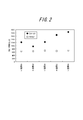
- FIG. 2 is a graph plotting the results of measuring the X-ray rocking curves ( ⁇ scan) of the (0002) plane and the (10-12) plane of the GaN channel layer for Experimental Examples 1-5.
- FIG. 3 shows the amount of warpage of the Si single crystal substrate for Experimental Examples 1-2 and 6-9, the horizontal axis represents the thickness of the second GaN layer of the first superlattice laminate, and the measured warpage amount and initial warpage. It is the graph which plotted the measurement result by making the difference with quantity into a vertical axis
- FIG. 4 is a graph showing the change in the half width when the number of sets of the second superlattice laminate is changed in Experimental Examples 1 and 2.
- FIG. 1 schematically shows a cross-sectional structure of a group III nitride epitaxial multilayer substrate for electronic devices according to the present invention.
- FIG. 1 shows the thickness direction exaggerated for convenience of explanation.
- the group III nitride epitaxial multilayer substrate 1 of the present invention epitaxially grows a substrate 2, a buffer 3 formed on the substrate 2, and a group III nitride layer on the buffer 3.
- the buffer 3 includes an initial growth layer 5 in contact with the substrate 2, a first superlattice laminate 6 formed on the initial growth layer 5, and the first superlattice laminate. 6 comprises a second superlattice laminate 7 formed on 6.
- the first superlattice laminate 6 is formed by alternately laminating a plurality of first AlN layers 6a made of an AlN material and second GaN layers 6b made of a GaN material.
- the AlN material and the GaN material mentioned in this specification are preferably AlN and GaN, but other group III elements in total of 5% or less (in the case of AlN material, in the case of B, Ga, In, and GaN materials) May contain B, Al, In).
- trace impurities such as Si, H, O, C, B, Mg, As, and P can be included.
- the second superlattice laminate 7 is formed by alternately laminating a plurality of first layers 7a made of an AlN material or an AlGaN material and a plurality of second layers 7b made of an AlGaN material having a band gap different from that of the first layer 7a.
- the “AlGaN material” in this specification is preferably AlGaN, but may contain other group III elements (B, In) in total of 5% or less. Further, for example, trace impurities such as Si, H, O, C, Mg, As, and P can be included.
- the group III nitride epitaxial multilayer substrate of the present invention is one of the characteristic configurations in that the first superlattice laminate is provided below the second superlattice laminate.
- the crystallinity of the group III nitride layer grown on the buffer can be improved without increasing the amount of warpage of the substrate.
- the warpage of the substrate can be suppressed more than the conventional one. Can do.
- the first superlattice laminate is configured as described above.
- the GaN material constituting the second GaN layer has a high lateral growth rate and a high effect of bending and extinguishing dislocations, and the AlN layer constituting the first AlN layer can further strengthen the strain in GaN. This is because the effect of the GaN material can be maximized.
- combining the second superlattice laminate with an AlN material having a larger band gap and a higher resistivity or an AlGaN material and an AlGaN material is preferable from the viewpoint of increasing the longitudinal breakdown voltage.
- the crystallinity in the present invention is evaluated by the full width at half maximum (FMHW) of the X-ray rocking curve ( ⁇ scan) of the (10-12) plane of the GaN channel layer as described in the experimental examples described later. Further, the warpage of the substrate is evaluated by the difference between the warpage amount of the Si single crystal substrate after the entire layer growth and the initial warpage amount, as described in an experimental example described later.
- FMHW full width at half maximum
- ⁇ scan X-ray rocking curve
- the substrate 2 is preferably a Si single crystal substrate.
- the plane orientation of the Si single crystal substrate is not particularly specified, and (111), (100), (110) planes, etc. can be used, but in order to grow the (0001) plane of group III nitride
- the (110) (111) plane is desirable for the surface, and it is desirable to use the (111) plane for growth with good surface flatness.
- the off angle is appropriately set at 1 ° or less so as not to impair the single crystal growth.
- any of the p-type and n-type conductivity types may be used, and it is applicable to various resistivities from 0.001 ⁇ cm to 100000 ⁇ cm. Further, the resistivity does not necessarily have to be uniform over the entire Si single crystal substrate.
- the Si single crystal substrate is a generic term for the case where the growth layer side is a single crystal substrate, and another substrate is bonded to the opposite side of the growth layer, or other materials such as an oxide film and a nitride film are used. The thing in which the film
- a typical material constituting the initial growth layer 5 is Al x Ga 1-x N (0.9 ⁇ x ⁇ 1.0).
- the substrate proximity portion of the initial growth layer 5 with an AlN material, reaction with the Si single crystal substrate can be suppressed, and the vertical breakdown voltage can be improved. It is possible to insert a thin film such as a Si nitride film, an oxide film, or a carbide film at the interface between the AlN and Si single crystal substrate, or insert a thin film obtained by reacting such a film with AlN.
- the initial growth layer 5 can be formed in an amorphous layer or a polycrystalline layer, such as a low-temperature buffer layer, with a thickness that does not impair the crystal quality. However, the initial growth layer 5 does not necessarily have a uniform composition in the film thickness direction. If the substrate proximity portion is made of an AlN material, a plurality of layers having different compositions can be laminated or the composition can be inclined.
- the MOCVD method As the growth method of each layer in the present invention, it is preferable to use the MOCVD method or the MBE method, which can easily ensure the interface steepness.
- the MOCVD method can be expected to improve the crystal quality of the present invention. This is because the MOCVD method has a higher lateral growth rate than the MBE method, so that the dislocation coalescence disappearance probability in the first superlattice laminate is high, and the crystal quality can be further improved.
- the pair of thicknesses of the first AlN layer 6a and the second GaN layer 6b (the thickness of the first AlN layer 6a + the thickness of the second GaN layer 6b) of the first superlattice laminate 6 is less than 44 nm, more preferably 24 nm or less. Preferably it is less than 10.5 nm.
- the thickness of the first AlN layer 6a is preferably 4 nm or less, and more preferably less than 4 nm. This is because if the set thickness of the first AlN layer 6a and the second GaN layer 6b or the thickness of the first AlN layer 6a is greater than or equal to the above thickness, the absolute value of the warp amount may increase.
- the film thickness of a 1st superlattice laminated body is restrict
- the number of pairs of the first AlN layer 6a and the second GaN layer 6b of the first superlattice laminate 6 is in the range of 5-20. If the number of sets exceeds 20, warping may increase, whereas if the number of sets is less than 5, even if inserted, the crystal quality improvement effect cannot be sufficiently expected.
- the first layer 7a of the second superlattice laminate 7 is made of an AlN material
- a compositional difference is required between the first layer 7a and the second layer 7b, so 0.1 ⁇ x ⁇ 0.5. Is more preferable. More preferably, 0.1 ⁇ x ⁇ 0.2.
- the number of sets of the first layer 7a and the second layer 7b of the second superlattice laminate 7 is preferably in the range of 40 to 300. If the number of sets exceeds 300, cracks may occur. On the other hand, if the number of sets is less than 40, there is a possibility that sufficient insulation cannot be ensured.
- each layer (first AlN layer 6a, second GaN layer 6b, first layer 7a, second layer 7b) constituting the first and second superlattice laminates 6 and 7 of the buffer 3 is 0.5 nm or more. It is preferable that This is because when the thickness is less than 0.5 nm, the thickness is less than one atomic layer.
- the buffer 3 is insulative and the lateral direction is the current conduction direction.
- the horizontal direction is the current conduction direction” means that a current flows mainly in the width direction of the stacked body.
- a structure in which a semiconductor is sandwiched between a pair of electrodes is mainly used in the vertical direction. That is, it means that the current flows differently from the thickness direction of the laminate.
- the average C concentration of the second superlattice laminate 7 is preferably 1 ⁇ 10 18 / cm 3 or more.
- the vertical breakdown voltage can be improved.
- the Al composition ratio x of the second layer 7b preferably exceeds 0.1 in order to efficiently mix C in order to ensure insulation.
- the average C concentration of the first superlattice is not particularly specified, but in order to further improve the vertical breakdown voltage, the average C concentration of the first superlattice is also set. It is preferable to be 1 ⁇ 10 18 / cm 3 or more.
- the “average C concentration” means a weighted average with respect to the thickness of the carbon concentration inside the laminate in which the first layers 7a and the second layers 7b are alternately laminated. It is assumed that a carbon concentration profile in the depth direction is measured while etching the film and is calculated based on the measurement result.
- the group III nitride epitaxial multilayer substrate 1 of the present invention can be used for any electronic device, and is particularly preferably used for HEMT.
- the electron supply layer 4b made of a material can be provided.
- both layers can be composed of a single composition or a plurality of compositions.
- at least a portion of the channel layer 4a in contact with the electron supply layer 4b is made of a GaN material.
- the portion of the channel layer 4a opposite to the buffer layer preferably has a low C concentration, and is preferably set to 3 ⁇ 10 16 / cm 3 or less. This is because this portion corresponds to a current conducting portion of the electronic device, and therefore it is desirable that no impurity that impedes conductivity or causes current collapse is included.
- FIG. 1 shows an example of a typical embodiment, and the present invention is not limited to this embodiment.
- an intermediate layer or other superlattice layer that does not adversely affect the effect of the present invention can be inserted between the layers, or the composition can be inclined.
- a nitride film, a carbonized film, an Al layer, or the like can be formed on the surface of the substrate.
- Example 1 An initial growth layer (AlN layer) in which AlN and Al 0.25 Ga 0.75 N are sequentially stacked as a buffer layer on a (111) plane 3-inch n-type Si single crystal substrate (Sb-doped specific resistance 0.015 ⁇ cm, thickness: 600 ⁇ m).
- Thickness 100 nm, Al 0.25 Ga 0.75 N thickness 40 nm
- first superlattice stack (20 sets of AlN / GaN, AlN thickness: 2 nm, GaN thickness: 6.5 nm
- second superlattice Lattice stacks 100 sets of AlN / Al 0.15 Ga 0.85 N, AlN thickness: 4 nm, AlGaN thickness: 25 nm
- a GaN channel is formed on the second superlattice stack as a main stack.
- a layer (thickness: 1.5 ⁇ m) and an Al 0.25 Ga 0.75 N electron supply layer (thickness: 30 nm) were epitaxially grown to produce a group III nitride epitaxial multilayer substrate having a HEMT structure.
- As a growth method an MOCVD method using TMA (trimethylaluminum), TMG (trimethylgallium), and ammonia as raw materials is used. Nitrogen / hydrogen was used as the carrier gas.
- the growth conditions (pressure and temperature) of each layer are as shown in Table 1.
- Example 2 A Group III nitride epitaxial multilayer substrate having a HEMT structure was produced in the same manner as in Experimental Example 1 except that the first superlattice laminate was not formed.
- Example 3 On a (111) plane 3 inch n-type Si single crystal substrate (thickness: 600 ⁇ m), as a buffer layer, an initial growth layer (thickness: 100 nm) made of an AlN material and a second superlattice laminate (AlN / Al 0.15 50 sets of Ga 0.85 N, AlN thickness: 4 nm, AlGaN thickness: 25 nm), first superlattice stack (20 sets of AlN / GaN, AlN thickness: 2 nm, GaN thickness: 6.
- the second superlattice laminate 50 sets of AlN / Al 0.15 Ga 0.85 N, AlN thickness: 4 nm, AlGaN thickness: 25 nm
- the main superlattice laminate is formed on the second superlattice laminate.
- a laminate a GaN channel layer (thickness: 1.5 ⁇ m) and an Al 0.25 Ga 0.75 N electron supply layer (thickness: 30 nm) were epitaxially grown to produce a group III nitride epitaxial multilayer substrate having a HEMT structure.
- Example 4 On a (111) plane 3 inch n-type Si single crystal substrate (thickness: 600 ⁇ m), as a buffer layer, an initial growth layer (thickness: 100 nm) made of an AlN material and a second superlattice laminate (AlN / Al 0.15 100 sets of Ga 0.85 N, AlN thickness: 4 nm, AlGaN thickness: 25 nm) and first superlattice stack (20 sets of AlN / GaN, AlN thickness: 2 nm, GaN thickness: 6.
- an initial growth layer made of an AlN material and a first superlattice laminate (AlN / GaN) 10 sets, AlN thickness: 2 nm, GaN thickness: 6.5 nm), second superlattice stack (100 sets of AlN / Al 0.15 Ga 0.85 N, AlN thickness: 4 nm, AlGaN thickness: 25 nm) and the first superlattice laminate (10 sets of AlN / GaN, AlN thickness: 2 nm, GaN thickness: 6.5 nm) are epitaxially grown, and the main laminate is formed on the first superlattice laminate.
- a GaN channel layer (thickness: 1.5 ⁇ m) and an Al 0.25 Ga 0.75 N electron supply layer (thickness: 30 nm) were epitaxially grown to produce a group III nitride epitaxial multilayer substrate having a HEMT structure.
- Example 6 A Group III nitride epitaxial multilayer substrate having a HEMT structure was produced in the same manner as in Experimental Example 1, except that the thickness of AlN of the first superlattice laminate was 4 nm.
- Example 7 A Group III nitride epitaxial multilayer substrate having a HEMT structure was produced in the same manner as in Experimental Example 1, except that the thickness of AlN in the first superlattice laminate was 4 nm and the thickness of GaN was 20 nm. .
- Example 8 A group III nitride epitaxial multilayer substrate having a HEMT structure was fabricated in the same manner as in Experimental Example 1, except that the thickness of AlN in the first superlattice laminate was 4 nm and the thickness of GaN was 40 nm. .
- Example 9 A Group III nitride epitaxial multilayer substrate having a HEMT structure was produced in the same manner as in Experimental Example 1, except that the thickness of AlN in the first superlattice laminate was 6 nm and the thickness of GaN was 40 nm. .
- Example 10 A group III nitride epitaxial multilayer substrate having a HEMT structure was produced in the same manner as in Experimental Example 1, except that the number of AlN / GaN pairs in the first superlattice laminate was five.
- Example 11 A group III nitride epitaxial multilayer substrate having a HEMT structure was produced in the same manner as in Experimental Example 1, except that the number of AlN / GaN pairs in the first superlattice laminate was 40.
- Example 12 A group III nitride epitaxial multilayer substrate having a HEMT structure was produced in the same manner as in Experimental Example 1, except that the number of AlN / GaN pairs in the first superlattice laminate was 100.
- FIG. 2 is a plot of the results of Experimental Examples 1-5.
- FIG. 2 shows that Experimental Example 1 is superior in crystallinity of the (10-12) plane as compared with Experimental Examples 2 to 5. Accordingly, only when the buffer layer has a layer configuration in which the initial growth layer, the first superlattice laminate, and the second superlattice laminate are formed in this order from the substrate side, the group III nitride formed thereon is formed. It can be seen that the effect of improving the crystallinity of the physical layer can be obtained.
- FIG. 3 is a plot of the results of Experimental Examples 1-2 and 6-9. As shown in Table 2, Experimental Examples 6 and 7 have better (10-12) plane crystallinity than Experimental Example 2. Also, from FIG. 3, compared with Experimental Examples 6 and 7, in Experimental Examples 8 and 9, the thickness of the first superlattice laminate is thick and the warpage cannot be sufficiently suppressed. That is, it can be seen that the warp amount of the Si single crystal substrate becomes smaller as the AlN thickness of the first superlattice laminate is smaller.
- Experimental Examples 10 to 12 have better (10-12) plane crystallinity than Experimental Example 2. For this reason, the crystallinity improvement effect of the present invention can be obtained from 5 pairs or more of the first superlattice laminate.
- Experimental Examples 11 and 12 have a large number of first superlattice laminates and cannot sufficiently suppress the warpage of the substrate. That is, it can be seen that the amount of warpage of the Si single crystal substrate is smaller when the number of first superlattice laminates is smaller.
- the first superlattice laminate, the second superlattice laminate, the GaN channel layer on the superlattice laminate side, and the GaN channel layer are analyzed by SIMS (secondary ion mass spectrometer).
- SIMS secondary ion mass spectrometer
- FIG. 4 shows the result of the same evaluation of the crystallinity of the (10-12) plane.
- the number of pairs of the second superlattice laminate regardless of the presence or absence of the first superlattice laminate, when the number of pairs is increased, the half-value width tends to decrease, and the first superlattice laminate is provided. It can be seen that the full width at half maximum is smaller compared to the case where the first superlattice laminate is not provided for any number of pairs.
- the amount of warpage when the number of sets of the second superlattice laminate is changed with respect to Experimental Example 1 (with the first superlattice laminate) (black circle in FIG. 4) is the amount of warpage of Experimental Example 1.
- the range is within ⁇ 5 ⁇ m with respect to (26 ⁇ m) ( The warpage amount of black triangles in FIG. 4 exceeded 5 ⁇ m from the warpage amount (25 ⁇ m) of Experimental Example 2.
- Example 3 Further, with respect to Experimental Example 1, except that the Al composition of the second superlattice laminate was changed, it was performed in the same manner as Experimental Example 1, and the crystallinity of the (10-12) plane was evaluated.
- the half-value width (10-12) which is an evaluation index of warpage and crystallinity
- the half-value width (10-12) which is an evaluation index of warpage and crystallinity
- the buffer is grown on the buffer without increasing the amount of warping of the substrate by providing the first superlattice stack between the initial growth layer and the second superlattice stack.
- the crystallinity of the group III nitride layer can be improved.
- Group III nitride epitaxial multilayer substrate 1 Group III nitride epitaxial multilayer substrate 2 Substrate 3 Buffer 4 Main laminate 4a Channel layer 4b Electron supply layer 5 Initial growth layer 6 First superlattice laminate 6a First AlN layer 6b Second GaN layer 7 Second superlattice laminate 7a 1st layer 7b 2nd layer
Landscapes
- Junction Field-Effect Transistors (AREA)
- Recrystallisation Techniques (AREA)
Abstract
Description
(1)基板と、該基板上に形成されたバッファと、該バッファ上にIII族窒化物層をエピタキシャル成長することにより形成された主積層体とを具えるIII族窒化物エピタキシャル積層基板であって、前記バッファは、前記基板と接する初期成長層ならびに該初期成長層上に形成された第1超格子積層体および該第1超格子積層体上に形成された第2超格子積層体からなり、前記第1超格子積層体は、AlN材料からなる第1AlN層およびGaN材料からなる第2GaN層を交互に5~20組積層してなり、かつ、前記第1AlN層および前記第2GaN層の1組の厚みが44nm未満であり、前記第2超格子積層体は、AlN材料またはAlGaN材料からなる第1層および該第1層とはバンドギャップの異なるAlGaN材料からなる第2層を交互に複数組積層してなることを特徴とするIII族窒化物エピタキシャル積層基板。
(実験例1)
(111)面3インチn型Si単結晶基板(Sbドープ比抵抗0.015Ωcm、厚さ:600μm)上に、バッファ層として、AlNとAl0.25Ga0.75Nを順に積層した初期成長層(AlNの厚さ:100nm、Al0.25Ga0.75Nの厚さ40nm)ならびに第1超格子積層体(AlN/GaNを20組、AlNの厚さ:2nm、GaNの厚さ:6.5nm)および第2超格子積層体(AlN/Al0.15Ga0.85Nを100組、AlNの厚さ:4nm、AlGaNの厚さ:25nm)をエピタキシャル成長させ、この第2超格子積層体上に、主積層体として、GaNチャネル層(厚さ:1.5μm)およびAl0.25Ga0.75N電子供給層(厚さ:30nm)をエピタキシャル成長させてHEMT構造を持つIII族窒化物エピタキシャル積層基板を作製した。成長方法としては、原料として、TMA(トリメチルアルミニウム)、TMG(トリメチルガリウム)、アンモニアを用いたMOCVD法を用いている。キャリアガスとしては、窒素・水素を用いた。各層の成長条件(圧力・温度)は表1に示す通りである。

上記第1超格子積層体を形成しなかったこと以外は、実験例1と同様の方法によりHEMT構造を持つIII族窒化物エピタキシャル積層基板を作製した。
(111)面3インチn型Si単結晶基板(厚さ:600μm)上に、バッファ層として、AlN材料からなる初期成長層(厚さ:100nm)ならびに第2超格子積層体(AlN/Al0.15Ga0.85Nを50組、AlNの厚さ:4nm、AlGaNの厚さ:25nm)、第1超格子積層体(AlN/GaNを20組、AlNの厚さ:2nm、GaNの厚さ:6.5nm)および第2超格子積層体(AlN/Al0.15Ga0.85Nを50組、AlNの厚さ:4nm、AlGaNの厚さ:25nm)をエピタキシャル成長させ、この第2超格子積層体上に、主積層体として、GaNチャネル層(厚さ:1.5μm)およびAl0.25Ga0.75N電子供給層(厚さ:30nm)をエピタキシャル成長させてHEMT構造を持つIII族窒化物エピタキシャル積層基板を作製した。
(111)面3インチn型Si単結晶基板(厚さ:600μm)上に、バッファ層として、AlN材料からなる初期成長層(厚さ:100nm)ならびに第2超格子積層体(AlN/Al0.15Ga0.85Nを100組、AlNの厚さ:4nm、AlGaNの厚さ:25nm)および第1超格子積層体(AlN/GaNを20組、AlNの厚さ:2nm、GaNの厚さ:6.5nm)をエピタキシャル成長させ、この第1超格子積層体上に、主積層体として、GaNチャネル層(厚さ:1.5μm)およびAl0.25Ga0.75N電子供給層(厚さ:30nm)をエピタキシャル成長させてHEMT構造を持つIII族窒化物エピタキシャル積層基板を作製した。
(111)面3インチn型Si単結晶基板(厚さ:600μm)上に、バッファ層として、AlN材料からなる初期成長層(厚さ:100nm)ならびに第1超格子積層体(AlN/GaNを10組、AlNの厚さ:2nm、GaNの厚さ:6.5nm)、第2超格子積層体(AlN/Al0.15Ga0.85Nを100組、AlNの厚さ:4nm、AlGaNの厚さ:25nm)および第1超格子積層体(AlN/GaNを10組、AlNの厚さ:2nm、GaNの厚さ:6.5nm)をエピタキシャル成長させ、この第1超格子積層体上に、主積層体として、GaNチャネル層(厚さ:1.5μm)およびAl0.25Ga0.75N電子供給層(厚さ:30nm)をエピタキシャル成長させてHEMT構造を持つIII族窒化物エピタキシャル積層基板を作製した。
上記第1超格子積層体のAlNの厚さを4nmとしたこと以外は、実験例1と同様の方法によりHEMT構造を持つIII族窒化物エピタキシャル積層基板を作製した。
上記第1超格子積層体のAlNの厚さを4nmとし、GaNの厚さを20nmとしたこと以外は、実験例1と同様の方法によりHEMT構造を持つIII族窒化物エピタキシャル積層基板を作製した。
上記第1超格子積層体のAlNの厚さを4nmとし、GaNの厚さを40nmとしたこと以外は、実験例1と同様の方法によりHEMT構造を持つIII族窒化物エピタキシャル積層基板を作製した。
上記第1超格子積層体のAlNの厚さを6nmとし、GaNの厚さを40nmとしたこと以外は、実験例1と同様の方法によりHEMT構造を持つIII族窒化物エピタキシャル積層基板を作製した。
上記第1の超格子積層体のAlN/GaNの組数を5組としたこと以外は、実験例1と同様の方法によりHEMT構造を持つIII族窒化物エピタキシャル積層基板を作製した。
上記第1の超格子積層体のAlN/GaNの組数を40組としたこと以外は、実験例1と同様の方法によりHEMT構造を持つIII族窒化物エピタキシャル積層基板を作製した。
上記第1の超格子積層体のAlN/GaNの組数を100組としたこと以外は、実験例1と同様の方法によりHEMT構造を持つIII族窒化物エピタキシャル積層基板を作製した。
実験例1~12について、X線回折装置(D8、Bruker社製)を用い、GaNチャネル層の(0002)面と(10-12)面のX線ロッキングカーブ(ωスキャン)を測定した。この(10-12)面のX線ロッキングカーブの半値幅(FMHW)は、III族窒化物層の結晶性を評価する指標となるものである。
結晶性の評価は、以下の通りである。
○:1100以下
△:1200-1100
×:1200以上
また、実験例1~12について、光干渉式の反り測定装置を用い、全層成長後のSi単結晶基板の反り量を測定し、初期反り量との差を計算し、評価した。
これらの結果を表2に示す。
なお、本実験例の範囲では、クラックは見られなかった。

図2は、実験例1~5の結果をプロットしたものである。図2から、実験例1は、実験例2~5と比較して、(10-12)面の結晶性に優れていることがわかる。このことから、バッファ層が、基板側から順に初期成長層、第1超格子積層体、第2超格子積層体の順に形成された層構成からなる場合にのみ、その上に形成したIII族窒化物層の結晶性向上の効果が得られることがわかる。すなわち、第1超格子積層体がない場合(実験例2)はもちろん、第1および第2超格子積層体の順序が逆の場合(実験例4)や、本発明に対して余分な超格子積層体を付加した場合(実験例3,5)においては、十分な結晶性を得ることができない。
図3は、実験例1~2、6~9の結果をプロットしたものである。
表2に示すように、実験例6,7は、実験例2と比較して、(10-12)面の結晶性が良い。また図3から、実験例6,7に比べて、実験例8,9では第1超格子積層体の膜厚が厚く、反りを十分抑制することができていない。すなわち、第1超格子積層体のAlNの厚さは薄い方がSi単結晶基板の反り量が小さくなることが分かる。
表2に示すように、実験例10~12は、実験例2と比較して、(10-12)面の結晶性が良い。このため、本発明の結晶性向上効果は、第1超格子積層体が5ペア以上から得ることができる。一方、実験例11,12は、第1超格子積層体の組数が多く、基板の反りを十分に抑制することができない。すなわち、第1超格子積層体の組数は少ない方がSi単結晶基板の反り量が小さくなることが分かる。
さらに、実験例1,2のIII族窒化物エピタキシャル積層基板について、ホール効果測定法により、チャネル部分の電気特性を評価したところ、ウェーハ中心でのシート抵抗は410Ω/□、移動度は1480cm2/Vsであった。
また、全ての実験例のエピタキシャル積層基板について、SIMS(二次イオン質量分析計)にて、第1超格子積層体、第2超格子積層体、GaNチャネル層の超格子積層体側、GaNチャネル層の電子供給層側のC濃度を評価したところ、それぞれ、8×10¹⁸/cm3、8×1018/cm3、1×1019/cm3、2×1016/cm3であり、縦方向の破壊耐圧は、700V以上であることが確認された。
実験例1,2に対して、第2超格子積層体の組数を変更させた以外は実験例1(第1超格子積層体あり),実験例2(第1超格子積層体なし)と同様に行い、(10-12)面の結晶性の評価を行った結果を、図4に示す。第2超格子積層体のペア数については、第1超格子積層体の有無に関わらず、ペア数を増加させると半値幅が減少するという傾向を示し、第1超格子積層体を設けた場合の方が、どのペア数においても第1超格子積層体を設けない場合に比べて半値幅が小さいことがわかる。また、実験例1(第1超格子積層体あり)に対して第2超格子積層体の組数を変化させた場合(図4中黒塗り丸)の反り量は、実験例1の反り量(26μm)に対して±5μm以内の範囲に抑えられていたのに対し、実験例2(第1超格子積層体なし)に対して第2超格子積層体の組数を変化させた場合(図4中黒塗り三角)の反り量は、実験例2の反り量(25μm)よりも5μmを超えた。
また、実験例1に対して、第2超格子積層体のAl組成を変更させた以外は、実験例1と同様に行い、(10-12)面の結晶性の評価を行った。第2超格子積層体をAlN/Al0.05Ga0.95N(x=0.05)とした場合、反り量と結晶性の評価指標である半値幅(10-12)は実験例1と同等の良好な結果が得られたが、半導体層表面に一部クラックが発生するものがあった。第2超格子積層体をAlN/Al0.2Ga0.8N(x=0.2)とした場合、反り量と結晶性の評価指標である半値幅(10-12)は実験例1と同等の良好な結果が得られ、半導体層表面にクラックが発生するものはなかった。
2 基板
3 バッファ
4 主積層体
4a チャネル層
4b 電子供給層
5 初期成長層
6 第1超格子積層体
6a 第1AlN層
6b 第2GaN層
7 第2超格子積層体
7a 第1層
7b 第2層
Claims (8)
- 基板と、該基板上に形成されたバッファと、該バッファ上にIII族窒化物層をエピタキシャル成長することにより形成された主積層体とを具えるIII族窒化物エピタキシャル積層基板であって、
前記バッファは、前記基板と接する初期成長層ならびに該初期成長層上に形成された第1超格子積層体および該第1超格子積層体上に形成された第2超格子積層体からなり、
前記第1超格子積層体は、AlN材料からなる第1AlN層およびGaN材料からなる第2GaN層を交互に5~20組積層してなり、かつ、前記第1AlN層および前記第2GaN層の1組の厚みが44nm未満であり、
前記第2超格子積層体は、AlN材料またはAlGaN材料からなる第1層および該第1層とはバンドギャップの異なるAlGaN材料からなる第2層を交互に複数組積層してなることを特徴とするIII族窒化物エピタキシャル積層基板。 - 前記第1超格子積層体の前記第1AlN層および前記第2GaN層の一組の厚みが、24nm以下で、かつ前記第1AlN層の厚みが4nm以下である請求項1に記載のIII族窒化物エピタキシャル積層基板。
- 前記第1超格子積層体の前記第1AlN層および前記第2GaN層の一組の厚みが、10.5nm未満で、かつ前記第1AlN層の厚みが4nm未満である請求項2に記載のIII族窒化物エピタキシャル積層基板。
- 前記第2超格子積層体の前記第1層がAlN材料からなり、前記第2層がAlxGayN(0<x<1, 0<y<1, x+y=1)材料からなる請求項1~3のいずれか一項に記載のIII族窒化物エピタキシャル積層基板。
- 前記第2超格子積層体の前記第1層および前記第2層の組数は、40~300の範囲である請求項1~4のいずれか一項に記載のIII族窒化物エピタキシャル積層基板。
- 前記バッファが絶縁性であり、横方向を電流導通方向とする請求項1~5のいずれか一項に記載のIII族窒化物エピタキシャル積層基板。
- 前記第2超格子積層体の平均C濃度が1×10¹⁸/cm3以上である請求項1~6のいずれか一項に記載のIII族窒化物エピタキシャル積層基板。
- 前記基板は、Si単結晶基板である請求項1~7のいずれか一項に記載のIII族窒化物エピタキシャル積層基板。
Priority Applications (4)
| Application Number | Priority Date | Filing Date | Title |
|---|---|---|---|
| EP10828104.9A EP2498282A4 (en) | 2009-11-04 | 2010-11-04 | EPITACTIC COATED GROUP III NITRIDE SUBSTRATE |
| US13/502,847 US8847203B2 (en) | 2009-11-04 | 2010-11-04 | Group III nitride epitaxial laminate substrate |
| CN201080060505.7A CN102714162B (zh) | 2009-11-04 | 2010-11-04 | 第iii族氮化物外延层压基板 |
| KR1020127012387A KR101358633B1 (ko) | 2009-11-04 | 2010-11-04 | Ⅲ족 질화물 에피택셜 적층 기판 |
Applications Claiming Priority (4)
| Application Number | Priority Date | Filing Date | Title |
|---|---|---|---|
| JP2009-253009 | 2009-11-04 | ||
| JP2009253009 | 2009-11-04 | ||
| JP2010-247432 | 2010-11-04 | ||
| JP2010247432A JP5576771B2 (ja) | 2009-11-04 | 2010-11-04 | Iii族窒化物エピタキシャル積層基板 |
Publications (1)
| Publication Number | Publication Date |
|---|---|
| WO2011055543A1 true WO2011055543A1 (ja) | 2011-05-12 |
Family
ID=43969785
Family Applications (1)
| Application Number | Title | Priority Date | Filing Date |
|---|---|---|---|
| PCT/JP2010/006504 Ceased WO2011055543A1 (ja) | 2009-11-04 | 2010-11-04 | Iii族窒化物エピタキシャル積層基板 |
Country Status (6)
| Country | Link |
|---|---|
| US (1) | US8847203B2 (ja) |
| EP (1) | EP2498282A4 (ja) |
| JP (1) | JP5576771B2 (ja) |
| KR (1) | KR101358633B1 (ja) |
| CN (1) | CN102714162B (ja) |
| WO (1) | WO2011055543A1 (ja) |
Cited By (4)
| Publication number | Priority date | Publication date | Assignee | Title |
|---|---|---|---|---|
| JP2013008836A (ja) * | 2011-06-24 | 2013-01-10 | Sharp Corp | 窒化物半導体装置 |
| JP2013128103A (ja) * | 2011-11-17 | 2013-06-27 | Sanken Electric Co Ltd | 窒化物半導体装置及び窒化物半導体装置の製造方法 |
| EP2525417A3 (en) * | 2011-05-16 | 2016-01-13 | Kabushiki Kaisha Toshiba | Nitride semiconductor device, nitride semiconductor wafer and method for manufacturing nitride semiconductor layer |
| CN111146269A (zh) * | 2018-11-06 | 2020-05-12 | 世界先进积体电路股份有限公司 | 高电子迁移率晶体管装置及其制造方法 |
Families Citing this family (44)
| Publication number | Priority date | Publication date | Assignee | Title |
|---|---|---|---|---|
| EP2538435B1 (en) * | 2010-02-16 | 2019-09-11 | NGK Insulators, Ltd. | Epitaxial substrate and method for producing same |
| JP5689245B2 (ja) * | 2010-04-08 | 2015-03-25 | パナソニック株式会社 | 窒化物半導体素子 |
| JPWO2011135963A1 (ja) * | 2010-04-28 | 2013-07-18 | 日本碍子株式会社 | エピタキシャル基板およびエピタキシャル基板の製造方法 |
| JP5891650B2 (ja) | 2011-08-18 | 2016-03-23 | 富士通株式会社 | 化合物半導体装置及びその製造方法 |
| WO2013137476A1 (ja) * | 2012-03-16 | 2013-09-19 | 次世代パワーデバイス技術研究組合 | 半導体積層基板、半導体素子、およびその製造方法 |
| WO2014024310A1 (ja) * | 2012-08-10 | 2014-02-13 | 日本碍子株式会社 | 半導体素子、hemt素子、および半導体素子の製造方法 |
| JP5425284B1 (ja) * | 2012-09-21 | 2014-02-26 | 株式会社東芝 | 半導体ウェーハ、半導体素子及び窒化物半導体層の製造方法 |
| JP2014072429A (ja) * | 2012-09-28 | 2014-04-21 | Fujitsu Ltd | 半導体装置 |
| JP2014072431A (ja) * | 2012-09-28 | 2014-04-21 | Fujitsu Ltd | 半導体装置 |
| KR101901932B1 (ko) | 2012-11-02 | 2018-09-27 | 엘지전자 주식회사 | 이종 기판, 질화물 반도체 발광 소자 및 그 제조 방법 |
| CN105264643B (zh) * | 2012-12-18 | 2019-11-08 | 爱思开矽得荣株式会社 | 半导体衬底及其制造方法 |
| US10256368B2 (en) | 2012-12-18 | 2019-04-09 | Sk Siltron Co., Ltd. | Semiconductor substrate for controlling a strain |
| JP5892971B2 (ja) * | 2013-04-09 | 2016-03-23 | 株式会社東芝 | 窒化物半導体層の製造方法 |
| JP6108609B2 (ja) * | 2013-04-25 | 2017-04-05 | クアーズテック株式会社 | 窒化物半導体基板 |
| CN110323268B (zh) | 2013-06-28 | 2023-01-03 | 英特尔公司 | 基于选择性外延生长的iii-v族材料的器件 |
| DE112014003533T5 (de) * | 2013-07-30 | 2016-04-14 | Sumitomo Chemical Company, Limited | Halbleiterwafer und Verfahren zur Herstellung des Halbleiterwafers |
| JP2015053328A (ja) * | 2013-09-05 | 2015-03-19 | 富士通株式会社 | 半導体装置 |
| JP6214978B2 (ja) * | 2013-09-17 | 2017-10-18 | 株式会社東芝 | 半導体装置 |
| JP2015070064A (ja) | 2013-09-27 | 2015-04-13 | 富士通株式会社 | 半導体装置及び半導体装置の製造方法 |
| JP2015176936A (ja) * | 2014-03-13 | 2015-10-05 | 株式会社東芝 | 半導体装置 |
| FR3028670B1 (fr) | 2014-11-18 | 2017-12-22 | Commissariat Energie Atomique | Structure semi-conductrice a couche de semi-conducteur du groupe iii-v ou ii-vi comprenant une structure cristalline a mailles cubiques ou hexagonales |
| US9337023B1 (en) * | 2014-12-15 | 2016-05-10 | Texas Instruments Incorporated | Buffer stack for group IIIA-N devices |
| US10109736B2 (en) * | 2015-02-12 | 2018-10-23 | Taiwan Semiconductor Manufacturing Co., Ltd. | Superlattice buffer structure for gallium nitride transistors |
| TWI566430B (zh) * | 2015-05-06 | 2017-01-11 | 嘉晶電子股份有限公司 | 氮化物半導體結構 |
| FR3041470B1 (fr) * | 2015-09-17 | 2017-11-17 | Commissariat Energie Atomique | Structure semi-conductrice a tenue en tension amelioree |
| US10529561B2 (en) * | 2015-12-28 | 2020-01-07 | Texas Instruments Incorporated | Method of fabricating non-etch gas cooled epitaxial stack for group IIIA-N devices |
| US20180151714A1 (en) * | 2016-11-30 | 2018-05-31 | Coorstek Kk | Nitride semiconductor substrate |
| TWI670852B (zh) | 2017-01-23 | 2019-09-01 | 比利時商愛美科公司 | 用於功率電子元件的三族氮化物基板及其製作方法 |
| US10535739B2 (en) | 2017-04-24 | 2020-01-14 | Enkris Semiconductor, Inc | Semiconductor structure and method of preparing semiconductor structure |
| TWI683372B (zh) * | 2017-06-29 | 2020-01-21 | 環球晶圓股份有限公司 | 半導體元件及其形成方法 |
| EP3451364B1 (en) * | 2017-08-28 | 2020-02-26 | Siltronic AG | Heteroepitaxial wafer and method for producing a heteroepitaxial wafer |
| US10516076B2 (en) | 2018-02-01 | 2019-12-24 | Silanna UV Technologies Pte Ltd | Dislocation filter for semiconductor devices |
| CN108550518B (zh) * | 2018-05-10 | 2020-03-24 | 南京大学 | 采用分子束外延技术生长用于缓解/消除铝镓氮薄膜表面裂纹的超晶格插入层的方法 |
| WO2020149729A1 (en) * | 2019-01-17 | 2020-07-23 | Collaborative Research In Engineering, Science And Technology Center | A method for growing a non-polar a-plane gallium nitride using aluminum nitride / gallium nitride superlattices |
| WO2020149730A1 (en) * | 2019-01-17 | 2020-07-23 | Collaborative Research In Engineering, Science And Technology Center | A method for growing a semi-polar gallium nitride epitaxial layer using aluminum nitride / gallium nitride superlattices |
| CN110643962A (zh) * | 2019-09-20 | 2020-01-03 | 深圳市晶相技术有限公司 | 一种半导体设备 |
| CN112820773B (zh) * | 2019-11-18 | 2024-05-07 | 联华电子股份有限公司 | 一种高电子迁移率晶体管 |
| FR3107051B1 (fr) * | 2020-02-12 | 2022-10-14 | Centre Nat Rech Scient | Procédé de fabrication de nanostructures de nitrure d’aluminium et de gallium (AlGaN) |
| TWI735212B (zh) * | 2020-04-24 | 2021-08-01 | 環球晶圓股份有限公司 | 具有超晶格疊層體的磊晶結構 |
| CN111902945B (zh) * | 2020-06-04 | 2022-05-20 | 英诺赛科(珠海)科技有限公司 | 半导体装置及其制造方法 |
| CN112928162B (zh) * | 2021-01-14 | 2023-06-09 | 华灿光电(浙江)有限公司 | 高电子迁移率晶体管外延片及其制备方法 |
| CN113161451B (zh) * | 2021-04-20 | 2023-02-28 | 湘能华磊光电股份有限公司 | 一种led外延结构及其生长方法 |
| JP7615947B2 (ja) * | 2021-07-29 | 2025-01-17 | 信越半導体株式会社 | 半導体デバイス用基板及びその製造方法 |
| CN113990940B (zh) * | 2021-08-30 | 2023-06-09 | 华灿光电(浙江)有限公司 | 碳化硅外延结构及其制造方法 |
Citations (5)
| Publication number | Priority date | Publication date | Assignee | Title |
|---|---|---|---|---|
| JP2003258005A (ja) * | 2002-03-07 | 2003-09-12 | National Institute Of Advanced Industrial & Technology | GaN系ヘテロ接合電界効果トランジスタ及びその特性を制御する方法 |
| WO2005015642A1 (ja) * | 2003-08-08 | 2005-02-17 | Sanken Electric Co., Ltd. | 半導体装置及びその製造方法 |
| JP2007067077A (ja) | 2005-08-30 | 2007-03-15 | Nippon Telegr & Teleph Corp <Ntt> | 窒化物半導体素子およびその製造方法 |
| JP2007142397A (ja) * | 2005-11-14 | 2007-06-07 | Palo Alto Research Center Inc | 半導体デバイス用超格子歪緩衝層 |
| JP2010251738A (ja) * | 2009-03-27 | 2010-11-04 | Covalent Materials Corp | 窒化物半導体エピタキシャル基板 |
Family Cites Families (11)
| Publication number | Priority date | Publication date | Assignee | Title |
|---|---|---|---|---|
| US5900071A (en) * | 1993-01-12 | 1999-05-04 | Massachusetts Institute Of Technology | Superlattice structures particularly suitable for use as thermoelectric materials |
| JP3609661B2 (ja) * | 1999-08-19 | 2005-01-12 | 株式会社東芝 | 半導体発光素子 |
| US7115896B2 (en) * | 2002-12-04 | 2006-10-03 | Emcore Corporation | Semiconductor structures for gallium nitride-based devices |
| US7119372B2 (en) * | 2003-10-24 | 2006-10-10 | Gelcore, Llc | Flip-chip light emitting diode |
| JP4826703B2 (ja) * | 2004-09-29 | 2011-11-30 | サンケン電気株式会社 | 半導体素子の形成に使用するための板状基体 |
| JP2007080996A (ja) * | 2005-09-13 | 2007-03-29 | Sony Corp | GaN系半導体発光素子及びその製造方法 |
| US7547925B2 (en) | 2005-11-14 | 2009-06-16 | Palo Alto Research Center Incorporated | Superlattice strain relief layer for semiconductor devices |
| US20090053845A1 (en) | 2005-11-14 | 2009-02-26 | Palo Alto Research Center Incorporated | Method For Controlling The Structure And Surface Qualities Of A Thin Film And Product Produced Thereby |
| US7501299B2 (en) | 2005-11-14 | 2009-03-10 | Palo Alto Research Center Incorporated | Method for controlling the structure and surface qualities of a thin film and product produced thereby |
| JP5309452B2 (ja) * | 2007-02-28 | 2013-10-09 | サンケン電気株式会社 | 半導体ウエーハ及び半導体素子及び製造方法 |
| EP2432005A4 (en) * | 2009-05-11 | 2015-05-27 | Dowa Electronics Materials Co Ltd | EPITACTICAL SUBSTRATE FOR ELECTRONIC EQUIPMENT AND METHOD FOR THE PRODUCTION THEREOF |
-
2010
- 2010-11-04 EP EP10828104.9A patent/EP2498282A4/en not_active Withdrawn
- 2010-11-04 CN CN201080060505.7A patent/CN102714162B/zh not_active Expired - Fee Related
- 2010-11-04 JP JP2010247432A patent/JP5576771B2/ja active Active
- 2010-11-04 US US13/502,847 patent/US8847203B2/en not_active Expired - Fee Related
- 2010-11-04 WO PCT/JP2010/006504 patent/WO2011055543A1/ja not_active Ceased
- 2010-11-04 KR KR1020127012387A patent/KR101358633B1/ko not_active Expired - Fee Related
Patent Citations (5)
| Publication number | Priority date | Publication date | Assignee | Title |
|---|---|---|---|---|
| JP2003258005A (ja) * | 2002-03-07 | 2003-09-12 | National Institute Of Advanced Industrial & Technology | GaN系ヘテロ接合電界効果トランジスタ及びその特性を制御する方法 |
| WO2005015642A1 (ja) * | 2003-08-08 | 2005-02-17 | Sanken Electric Co., Ltd. | 半導体装置及びその製造方法 |
| JP2007067077A (ja) | 2005-08-30 | 2007-03-15 | Nippon Telegr & Teleph Corp <Ntt> | 窒化物半導体素子およびその製造方法 |
| JP2007142397A (ja) * | 2005-11-14 | 2007-06-07 | Palo Alto Research Center Inc | 半導体デバイス用超格子歪緩衝層 |
| JP2010251738A (ja) * | 2009-03-27 | 2010-11-04 | Covalent Materials Corp | 窒化物半導体エピタキシャル基板 |
Non-Patent Citations (1)
| Title |
|---|
| See also references of EP2498282A4 |
Cited By (4)
| Publication number | Priority date | Publication date | Assignee | Title |
|---|---|---|---|---|
| EP2525417A3 (en) * | 2011-05-16 | 2016-01-13 | Kabushiki Kaisha Toshiba | Nitride semiconductor device, nitride semiconductor wafer and method for manufacturing nitride semiconductor layer |
| JP2013008836A (ja) * | 2011-06-24 | 2013-01-10 | Sharp Corp | 窒化物半導体装置 |
| JP2013128103A (ja) * | 2011-11-17 | 2013-06-27 | Sanken Electric Co Ltd | 窒化物半導体装置及び窒化物半導体装置の製造方法 |
| CN111146269A (zh) * | 2018-11-06 | 2020-05-12 | 世界先进积体电路股份有限公司 | 高电子迁移率晶体管装置及其制造方法 |
Also Published As
| Publication number | Publication date |
|---|---|
| JP5576771B2 (ja) | 2014-08-20 |
| EP2498282A4 (en) | 2014-06-25 |
| US20120223328A1 (en) | 2012-09-06 |
| CN102714162A (zh) | 2012-10-03 |
| EP2498282A1 (en) | 2012-09-12 |
| KR101358633B1 (ko) | 2014-02-04 |
| KR20120098689A (ko) | 2012-09-05 |
| US8847203B2 (en) | 2014-09-30 |
| CN102714162B (zh) | 2015-04-29 |
| JP2011119715A (ja) | 2011-06-16 |
Similar Documents
| Publication | Publication Date | Title |
|---|---|---|
| JP5576771B2 (ja) | Iii族窒化物エピタキシャル積層基板 | |
| US10727303B2 (en) | Group III nitride epitaxial substrate and method for manufacturing the same | |
| US8426893B2 (en) | Epitaxial substrate for electronic device and method of producing the same | |
| JP5462377B1 (ja) | Iii族窒化物エピタキシャル基板およびその製造方法 | |
| JP6408344B2 (ja) | Iii族窒化物半導体エピタキシャル基板およびその製造方法、ならびにiii族窒化物半導体発光素子 | |
| JP5818853B2 (ja) | n型窒化アルミニウム単結晶基板を用いた縦型窒化物半導体デバイス | |
| US8946723B2 (en) | Epitaxial substrate and method for manufacturing epitaxial substrate | |
| EP2565906A1 (en) | Epitaxial substrate and process for producing epitaxial substrate | |
| EP2565928A1 (en) | Epitaxial substrate and method for producing epitaxial substrate | |
| US20120126239A1 (en) | Layer structures for controlling stress of heteroepitaxially grown iii-nitride layers | |
| TWI657578B (zh) | 半導體基板及半導體基板的檢查方法 | |
| JP5334057B2 (ja) | Iii族窒化物積層基板 | |
| CN102891174A (zh) | 包括氮化物基半导体层的外延片 | |
| WO2011122322A1 (ja) | エピタキシャル基板およびエピタキシャル基板の製造方法 | |
| JP5662184B2 (ja) | 半導体素子用のエピタキシャル基板、および半導体素子用エピタキシャル基板の製造方法 | |
| JP6595682B2 (ja) | Iii族窒化物半導体発光素子 | |
| KR20140022136A (ko) | 반도체 발광소자 | |
| JP2016184663A (ja) | 半導体ウエハ、半導体装置及び半導体ウエハの製造方法 | |
| JP2008085123A (ja) | 化合物半導体デバイス用基板およびそれを用いた化合物半導体デバイス |
Legal Events
| Date | Code | Title | Description |
|---|---|---|---|
| WWE | Wipo information: entry into national phase |
Ref document number: 201080060505.7 Country of ref document: CN |
|
| 121 | Ep: the epo has been informed by wipo that ep was designated in this application |
Ref document number: 10828104 Country of ref document: EP Kind code of ref document: A1 |
|
| REEP | Request for entry into the european phase |
Ref document number: 2010828104 Country of ref document: EP |
|
| WWE | Wipo information: entry into national phase |
Ref document number: 2010828104 Country of ref document: EP |
|
| NENP | Non-entry into the national phase |
Ref country code: DE |
|
| WWE | Wipo information: entry into national phase |
Ref document number: 13502847 Country of ref document: US |
|
| ENP | Entry into the national phase |
Ref document number: 20127012387 Country of ref document: KR Kind code of ref document: A |