WO2011055845A1 - 磁性部材および電子部品 - Google Patents
磁性部材および電子部品 Download PDFInfo
- Publication number
- WO2011055845A1 WO2011055845A1 PCT/JP2010/069945 JP2010069945W WO2011055845A1 WO 2011055845 A1 WO2011055845 A1 WO 2011055845A1 JP 2010069945 W JP2010069945 W JP 2010069945W WO 2011055845 A1 WO2011055845 A1 WO 2011055845A1
- Authority
- WO
- WIPO (PCT)
- Prior art keywords
- magnetic member
- magnetic
- superparamagnetic particles
- superparamagnetic
- particle
- Prior art date
- Legal status (The legal status is an assumption and is not a legal conclusion. Google has not performed a legal analysis and makes no representation as to the accuracy of the status listed.)
- Ceased
Links
Images



Classifications
-
- H—ELECTRICITY
- H01—ELECTRIC ELEMENTS
- H01F—MAGNETS; INDUCTANCES; TRANSFORMERS; SELECTION OF MATERIALS FOR THEIR MAGNETIC PROPERTIES
- H01F1/00—Magnets or magnetic bodies characterised by the magnetic materials therefor; Selection of materials for their magnetic properties
- H01F1/0018—Diamagnetic or paramagnetic materials, i.e. materials with low susceptibility and no hysteresis
-
- B—PERFORMING OPERATIONS; TRANSPORTING
- B22—CASTING; POWDER METALLURGY
- B22F—WORKING METALLIC POWDER; MANUFACTURE OF ARTICLES FROM METALLIC POWDER; MAKING METALLIC POWDER; APPARATUS OR DEVICES SPECIALLY ADAPTED FOR METALLIC POWDER
- B22F1/00—Metallic powder; Treatment of metallic powder, e.g. to facilitate working or to improve properties
- B22F1/05—Metallic powder characterised by the size or surface area of the particles
- B22F1/054—Nanosized particles
-
- H—ELECTRICITY
- H01—ELECTRIC ELEMENTS
- H01F—MAGNETS; INDUCTANCES; TRANSFORMERS; SELECTION OF MATERIALS FOR THEIR MAGNETIC PROPERTIES
- H01F1/00—Magnets or magnetic bodies characterised by the magnetic materials therefor; Selection of materials for their magnetic properties
- H01F1/0036—Magnets or magnetic bodies characterised by the magnetic materials therefor; Selection of materials for their magnetic properties showing low dimensional magnetism, i.e. spin rearrangements due to a restriction of dimensions, e.g. showing giant magnetoresistivity
- H01F1/0045—Zero dimensional, e.g. nanoparticles, soft nanoparticles for medical/biological use
- H01F1/0054—Coated nanoparticles, e.g. nanoparticles coated with organic surfactant
-
- H—ELECTRICITY
- H01—ELECTRIC ELEMENTS
- H01F—MAGNETS; INDUCTANCES; TRANSFORMERS; SELECTION OF MATERIALS FOR THEIR MAGNETIC PROPERTIES
- H01F1/00—Magnets or magnetic bodies characterised by the magnetic materials therefor; Selection of materials for their magnetic properties
- H01F1/0036—Magnets or magnetic bodies characterised by the magnetic materials therefor; Selection of materials for their magnetic properties showing low dimensional magnetism, i.e. spin rearrangements due to a restriction of dimensions, e.g. showing giant magnetoresistivity
- H01F1/0045—Zero dimensional, e.g. nanoparticles, soft nanoparticles for medical/biological use
- H01F1/0063—Zero dimensional, e.g. nanoparticles, soft nanoparticles for medical/biological use in a non-magnetic matrix, e.g. granular solids
-
- H—ELECTRICITY
- H01—ELECTRIC ELEMENTS
- H01F—MAGNETS; INDUCTANCES; TRANSFORMERS; SELECTION OF MATERIALS FOR THEIR MAGNETIC PROPERTIES
- H01F1/00—Magnets or magnetic bodies characterised by the magnetic materials therefor; Selection of materials for their magnetic properties
- H01F1/01—Magnets or magnetic bodies characterised by the magnetic materials therefor; Selection of materials for their magnetic properties of inorganic materials
- H01F1/03—Magnets or magnetic bodies characterised by the magnetic materials therefor; Selection of materials for their magnetic properties of inorganic materials characterised by their coercivity
- H01F1/12—Magnets or magnetic bodies characterised by the magnetic materials therefor; Selection of materials for their magnetic properties of inorganic materials characterised by their coercivity of soft-magnetic materials
- H01F1/34—Magnets or magnetic bodies characterised by the magnetic materials therefor; Selection of materials for their magnetic properties of inorganic materials characterised by their coercivity of soft-magnetic materials non-metallic substances, e.g. ferrites
- H01F1/36—Magnets or magnetic bodies characterised by the magnetic materials therefor; Selection of materials for their magnetic properties of inorganic materials characterised by their coercivity of soft-magnetic materials non-metallic substances, e.g. ferrites in the form of particles
- H01F1/37—Magnets or magnetic bodies characterised by the magnetic materials therefor; Selection of materials for their magnetic properties of inorganic materials characterised by their coercivity of soft-magnetic materials non-metallic substances, e.g. ferrites in the form of particles in a bonding agent
-
- H—ELECTRICITY
- H01—ELECTRIC ELEMENTS
- H01F—MAGNETS; INDUCTANCES; TRANSFORMERS; SELECTION OF MATERIALS FOR THEIR MAGNETIC PROPERTIES
- H01F27/00—Details of transformers or inductances, in general
- H01F27/24—Magnetic cores
- H01F27/255—Magnetic cores made from particles
-
- H—ELECTRICITY
- H01—ELECTRIC ELEMENTS
- H01F—MAGNETS; INDUCTANCES; TRANSFORMERS; SELECTION OF MATERIALS FOR THEIR MAGNETIC PROPERTIES
- H01F3/00—Cores, Yokes, or armatures
- H01F3/08—Cores, Yokes, or armatures made from powder
-
- H—ELECTRICITY
- H01—ELECTRIC ELEMENTS
- H01F—MAGNETS; INDUCTANCES; TRANSFORMERS; SELECTION OF MATERIALS FOR THEIR MAGNETIC PROPERTIES
- H01F41/00—Apparatus or processes specially adapted for manufacturing or assembling magnets, inductances or transformers; Apparatus or processes specially adapted for manufacturing materials characterised by their magnetic properties
- H01F41/02—Apparatus or processes specially adapted for manufacturing or assembling magnets, inductances or transformers; Apparatus or processes specially adapted for manufacturing materials characterised by their magnetic properties for manufacturing cores, coils, or magnets
-
- B—PERFORMING OPERATIONS; TRANSPORTING
- B82—NANOTECHNOLOGY
- B82Y—SPECIFIC USES OR APPLICATIONS OF NANOSTRUCTURES; MEASUREMENT OR ANALYSIS OF NANOSTRUCTURES; MANUFACTURE OR TREATMENT OF NANOSTRUCTURES
- B82Y25/00—Nanomagnetism, e.g. magnetoimpedance, anisotropic magnetoresistance, giant magnetoresistance or tunneling magnetoresistance
-
- B—PERFORMING OPERATIONS; TRANSPORTING
- B82—NANOTECHNOLOGY
- B82Y—SPECIFIC USES OR APPLICATIONS OF NANOSTRUCTURES; MEASUREMENT OR ANALYSIS OF NANOSTRUCTURES; MANUFACTURE OR TREATMENT OF NANOSTRUCTURES
- B82Y30/00—Nanotechnology for materials or surface science, e.g. nanocomposites
Definitions
- the present invention relates to a magnetic member.
- the position of each superparamagnetic particle is held by the solid, so even when an AC magnetic field is applied from the outside during use, the superparamagnetic particle itself is not displaced, that is, not magnetized or demagnetized by the Brownian mechanism.
- the magnetic response of the superparamagnetic particles depends on the displacement of the magnetic moment inherent in the particles, that is, the magnetization and demagnetization by the Neil mechanism.
- the magnetic member described above when the period P of the alternating magnetic field applied from the outside at the time of use is shorter than the time (relaxation time) ⁇ required for magnetization and demagnetization by the Neil mechanism, the magnetic response of the superparamagnetic particles is It cannot keep up with this period P. As a result, the magnetic member described above may lose superparamagnetic properties and cause magnetic hysteresis.
- an object of the present invention is to provide a magnetic member that does not lose its superparamagnetic characteristics when used and does not cause magnetic hysteresis.
- a first aspect of the present invention for solving the above problem is a magnetic member, comprising a plurality of superparamagnetic particles held by the magnetic member, and each of the plurality of superparamagnetic particles is at least each of the above. Particles determined so that the Neil relaxation time ⁇ n of the superparamagnetic particles is shorter than the period P of the alternating magnetic field applied to the magnetic member when the magnetic member is used as the electronic component ( ⁇ n ⁇ P). It is formed with a diameter.
- each of the plurality of superparamagnetic particles is held, and therefore, when a signal is applied from the outside during use, the superparamagnetic particles themselves are displaced, that is, magnetized and demagnetized by the Brownian mechanism. Limited. Therefore, the magnetic response of superparamagnetic particles depends on the displacement of the magnetic moment inherent in the particles, that is, the magnetization and demagnetization by the Neil mechanism.
- each of the superparamagnetic particles is at least The particle diameter is determined so that the Neal relaxation time ⁇ n in the superparamagnetic particles is shorter than the period P of the signal applied during use ( ⁇ n ⁇ P). For this reason, the period P of the alternating magnetic field applied from the outside at the time of use does not become shorter than the relaxation time ⁇ , and the magnetic response does not catch up with the period P, resulting in magnetic hysteresis. Absent.
- the superparamagnetic particles in order to hold each of the superparamagnetic particles, for example, the superparamagnetic particles may be made non-displaceable by directly or indirectly contacting each other, or using any base material. It may be impossible to displace.
- the magnetic member of the first aspect may be configured as the magnetic member of the second aspect of the present invention described below.
- each of the superparamagnetic particles is in a state in which the displacement by the Brownian mechanism is limited by dispersing the respective superparamagnetic particles in a base material that can suppress the displacement by the Brownian mechanism. Is held by.
- the magnetic member of the second aspect in order to disperse each of the superparamagnetic particles in the solid base material, the magnetic member of the second aspect may be configured as the magnetic member of the third aspect, for example.
- the base material is a non-magnetic member, and the member is solidified after the respective superparamagnetic particles are dispersed in the member in a liquefied state. Each superparamagnetic particle is retained.
- each superparamagnetic particle can be dispersed in a solid substrate by dispersing each superparamagnetic particle in a liquefied member and then solidifying the member.
- each superparamagnetic particle may be formed with a nonmagnetic coating layer on the surface of each superparamagnetic particle, like the magnetic member of the fourth aspect.
- the magnetic member configured as described above, since the non-magnetic coating layer is formed on each superparamagnetic particle, the superparamagnetic particle when each superparamagnetic particle is dispersed in a liquefied base material. Thus, it is possible to reliably hold the superparamagnetic particles in the solidified base material.
- a fifth aspect of the present invention is an electronic component comprising a magnetic core, and any one magnetic member of the first to fourth aspects is used for the magnetic core. If it is this electronic component, the effect
- This electronic component may be used as any one of a magnetic sensor, a chip antenna, a transformer, and an inductor.
- FIG. 2A is a graph showing the change in relaxation time according to the particle size at each of a plurality of temperatures
- FIG. 2B is a graph showing the relaxation time according to the particle size at each of a plurality of anisotropic constants.
- FIGS. 3A and 3B are views showing a first example of a magnetic sensor for current detection to which a magnetic member according to the present invention is applied
- FIG. 3A is a perspective view of the sensor
- FIG. 3B is a cross-sectional view taken along line AA in FIG. FIG.
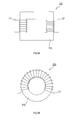
- FIG. 9A is a diagram illustrating an example of a transformer to which the magnetic member according to the present invention is applied
- FIG. 9B is a diagram illustrating an example of an inductor to which the magnetic member according to the present invention is applied.
- the magnetic member is a member that holds each of a plurality of superparamagnetic particles, and constitutes a part of the electronic component.
- the particle diameter of each superparamagnetic particle is determined according to the speed of magnetic response.
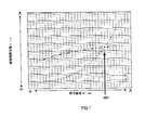
- the magnetic response is due to the Brown mechanism in which the particle itself is inverted and the Neil mechanism in which the magnetic spin in the particle is inverted. As shown in FIG. 1, the speed is inverted in each of the Brown mechanism and the Neil mechanism. Determined by time (relaxation time) ⁇ .
- the relaxation time ⁇ becomes longer depending on the particle diameter d of the superparamagnetic particles.
- the relaxation time ⁇ n based on the Neel mechanism has a larger fluctuation range depending on the particle diameter than the relaxation time ⁇ b based on the Brown mechanism.
- it is smaller than the relaxation time ⁇ b until the diameter dth is exceeded, after the particle diameter dth is exceeded, it becomes longer than the relaxation time ⁇ b. That is, if the particle size dth is not exceeded, the magnetic response in the Neil mechanism is faster than that in the Brownian mechanism, and the magnetic response in the Neil mechanism becomes dominant. The response is slower and the magnetic response by the Brownian mechanism becomes dominant.
- the relaxation time ⁇ n by the Neil mechanism is obtained by the following formula 1, and excluding constants (including those that can be regarded as constants), it depends on the temperature T, the anisotropic constant ITA, and the particle size R. It becomes a determined value.
- FIG. 2A is based on this equation 1 and corresponds to the particle diameter R at each of a plurality of temperatures T (in this embodiment, ⁇ 40 ° C. ( ⁇ 233 K), 25 ° C. ( ⁇ 298 K), 130 ° C. ( ⁇ 403 K)).
- FIG. 2B is a graph showing a change in the relaxation time ⁇ n, and FIG. 2B shows a relaxation time ⁇ n according to the particle size R in each of a plurality of anisotropic constants excellent (30, 41, 50, 60, and 70 in this embodiment). It is a graph showing. In these examples, 10 ⁇ (-9) sec is used as the reference relaxation time ⁇ 0 when an iron oxide-based material is used as the superparamagnetic particles.
- At least the neil relaxation time ⁇ n in the superparamagnetic particles is shorter than the period P of the alternating magnetic field applied to the magnetic member when the magnetic member is used as an electronic component.
- the particle size of the superparamagnetic particles is determined as ( ⁇ n ⁇ P).
- each of the superparamagnetic particles is held so that displacement by the Brownian mechanism is limited (in this embodiment, suppressed). More specifically, the magnetic member of this embodiment should just be the structure hold
- indirect contact refers to contact in a state where a film is formed on the surface of the superparamagnetic particle or some medium is interposed.
- each of the superparamagnetic particles is dispersed in a substrate capable of suppressing the displacement by the Brownian mechanism, so that each of the superparamagnetic particles is restricted so that the displacement by the Brownian mechanism is limited. It is good also as a hold
- the magnetic member is made of a non-magnetic member (for example, resin material, ceramic, etc.) as a base material, and the superparamagnetic particles are dispersed in the member in a liquefied state, and the magnetic member has a fixed positional relationship. Superparamagnetic particles may be retained by solidifying the member.
- a gel-like or highly viscous liquid can be employed as the base material.
- Each superparamagnetic particle only needs to have a positional relationship that does not impair the superparamagnetic characteristics of adjacent superparamagnetic particles by more than a predetermined threshold, and the concentration at which the positional relationship is maintained is limited to an upper limit. As dispersed in the substrate.
- a plurality of magnetic members 1 arranged in parallel with each other and formed in an annular shape, a plurality of excitation coils 12 wound around the entire circumference of each magnetic member 1, and a plurality of A magnetic sensor for current detection provided with a detection coil 14 wound around each of the magnetic members 1 can be considered.
- the current flowing through the conductor 18 that has passed through the annular portion of the plurality of magnetic members 1 is detected.
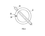
- the magnetic member 2 is formed in an annular shape, and the magnetic member 2 in which a gap 22 is formed in a part of the magnetic member 2, and the Hall element 24 arranged in the gap 22.
- a magnetic sensor for current detection provided with This magnetic sensor detects a current flowing in the conducting wire 28 passed through the annular portion of the magnetic member 2.
- the magnetic member 3 is formed in an annular shape, the magnetic member 3 having a gap 34 formed in a part of the magnetic member 3, and the equilibrium wound around the entire circumference of the magnetic member 3.
- a magnetic sensor for current detection including a coil 32 and a hall element 36 disposed in the gap 34 of the magnetic member 3 can be considered. This magnetic sensor detects a current flowing in the conducting wire 38 that is passed through the annular portion of the magnetic member 3.
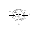
- the magnetic member 4 formed in an annular shape, a coupling magnetic path 42 that connects the annular portion of the magnetic member 4 so as to be divided, and an excitation coil wound around the entire circumference of the magnetic member 4
- a magnetic sensor for current detection including 44 and a detection coil 46 wound over the entire length of the coupling magnetic path 42 can be considered.
- This magnetic sensor detects a current flowing through a conducting wire 48 that passes through an annular portion of the magnetic member 4 from one region divided by the coupling magnetic path 42 to the other region.
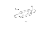
- a ferrite bead configured by a magnetic member 5 formed in a cylindrical shape and having a conductive wire 52 penetrated through the cylindrical portion is conceivable.
- this ferrite bead even if high-frequency noise such as a steep spike is generated in the conductor 52 by using the magnetic member 5 having a high magnetic permeability with respect to a high frequency, the magnetic member 5 Since high impedance resulting from magnetic permeability is exhibited, propagation of such high-frequency noise to the conductor 52 can be suppressed.
- the columnar magnetic member A configuration in which a spiral conductor is embedded inside may be included.
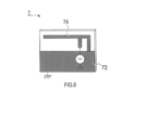
- a magnetic member 7 formed in a rectangular plate shape is provided, and a grounding conductor 72 extending in the left-right direction is provided in a lower region on the plate-shaped surface, and left and right in other regions.
- a chip antenna provided with an antenna conductor 74 extending in the direction is conceivable.
- the antenna conductor 74 is formed in an F shape, but the shape as the antenna conductor is not limited to this shape.
- one end side of the antenna conductor 74 is connected to the ground conductor 72, but this one end side is not necessarily connected to the ground conductor 72.
- the electronic component to which the magnetic member described above is applied may include electronic components other than the magnetic sensor such as a transformer and an inductor in addition to the electronic component described above.
- a winding L1 and a winding L2 are wound around an annular magnetic member 110 having a square planar shape like a transformer 100 shown in FIG. 9A. It may be formed.
- the inductor to which the above-described magnetic member is applied may be formed by winding a winding L3 around an annular magnetic member 210, for example, like an inductor 200 shown in FIG. 9B.
- each superparamagnetic particle is held. Therefore, when a signal is applied from the outside during use, the displacement of the superparamagnetic particle itself, that is, the magnetization by the Brownian mechanism And demagnetization is limited. Therefore, the magnetic response of superparamagnetic particles depends on the displacement of the magnetic moment inherent in the particles, that is, the magnetization and demagnetization by the Neil mechanism.
- each superparamagnetic particle is at least the Neil in the superparamagnetic particle.
- the particle size is determined such that the relaxation time ⁇ n is shorter than the period P of the signal applied during use ( ⁇ n ⁇ P). For this reason, the period P of the alternating magnetic field applied from the outside at the time of use does not become shorter than the relaxation time ⁇ , and the magnetic response does not catch up with the period P, resulting in magnetic hysteresis. Absent.
- each of the superparamagnetic particles when each of the superparamagnetic particles is dispersed in the substrate capable of suppressing the displacement due to the Brownian mechanism, each of the superparamagnetic particles is dispersed in the substrate, and the displacement due to the Brownian mechanism is limited. Each of the superparamagnetic particles can be held in a state.
- the superparamagnetic particles when each of the superparamagnetic particles is dispersed in the member in a state in which the substrate that is a nonmagnetic member is liquefied and then solidified, the superparamagnetic particles are each solid substrate. Can be dispersed in.
- the presence of the nonmagnetic coating layer allows the superparamagnetic particles to be liquefied in the base material.
- the affinity of both the superparamagnetic particles and the base material when dispersed in the base material can be increased, whereby each superparamagnetic particle can be reliably held in the solidified base material.
Landscapes
- Engineering & Computer Science (AREA)
- Chemical & Material Sciences (AREA)
- Nanotechnology (AREA)
- Power Engineering (AREA)
- Molecular Biology (AREA)
- General Health & Medical Sciences (AREA)
- Biomedical Technology (AREA)
- Life Sciences & Earth Sciences (AREA)
- Health & Medical Sciences (AREA)
- Inorganic Chemistry (AREA)
- Crystallography & Structural Chemistry (AREA)
- Physics & Mathematics (AREA)
- Materials Engineering (AREA)
- General Physics & Mathematics (AREA)
- Condensed Matter Physics & Semiconductors (AREA)
- Composite Materials (AREA)
- Dispersion Chemistry (AREA)
- Manufacturing & Machinery (AREA)
- Soft Magnetic Materials (AREA)
- Measuring Magnetic Variables (AREA)
- Coils Or Transformers For Communication (AREA)
- Hall/Mr Elements (AREA)
Abstract
Description
また、この第2局面の磁性部材において、固体の基材中に超常磁性粒子それぞれを分散させるためには、第2局面の磁性部材を例えば、第3局面の磁性部材のように構成するとよい。
(1)磁性部材の特徴
磁性部材は、複数の超常磁性粒子それぞれを保持した部材であり、電子部品の一部を構成するものである。この超常磁性粒子それぞれの粒径は、磁気応答の速度に応じて定められている。

(2)具体的な適用構成
上述した磁性部材を適用する電子部品としては、例えば、以下に示すようなものが考えられる。
(3)作用,効果
このように構成された磁性部材では、超常磁性粒子それぞれが保持されているため、使用時に外部から信号を印加した場合に、超常磁性粒子自体の変位、つまりブラウン機構による磁化および消磁が制限される。そのため、超常磁性粒子の磁気応答は、粒子に内在する磁気モーメントの変位、つまりニール機構による磁化および消磁に依存する。
Claims (6)
- 磁性部材であって、
前記磁性部材に保持された複数の超常磁性粒子を備え、
前記複数の超常磁性粒子のそれぞれは、少なくとも、該それぞれの超常磁性粒子におけるニール緩和時間τnが、前記磁性部材が電子部品として用いられる際に当該磁性部材に印加される交流磁界の周期Pよりも短くなる(τn<P)ように定められた粒径で形成されている
ことを特徴とする磁性部材。 - 前記それぞれの超常磁性粒子は、当該それぞれの超常磁性粒子を、ブラウン機構による変位を抑制可能な基材中に分散させることにより、ブラウン機構による変位が制限された状態で保持されている
ことを特徴とする請求項1に記載の磁性部材。 - 前記基材は、非磁性の部材であり、該部材を液化した状態で該部材に前記それぞれの超常磁性粒子を分散させてから該部材を固化することによって、前記それぞれの超常磁性粒子を保持している
ことを特徴とする請求項2に記載の磁性部材。 - 前記それぞれの超常磁性粒子は、該それぞれの超常磁性粒子の表面に非磁性のコーティング層が形成されている
ことを特徴とする請求項2または請求項3に記載の磁性部材。 - 電子部品であって、
磁心を備え、
前記磁心には、請求項1から4のいずれかに記載の磁性部材が用いられている
ことを特徴とする電子部品。 - 磁気センサと、チップアンテナと、トランスと、インダクタとのうちのいずれか1つとして用いられている
ことを特徴とする請求項5に記載の電子部品。
Priority Applications (5)
| Application Number | Priority Date | Filing Date | Title |
|---|---|---|---|
| KR1020127014736A KR101778319B1 (ko) | 2009-11-09 | 2010-11-09 | 자성 부재 및 전자 부품 |
| US13/508,616 US9627111B2 (en) | 2009-11-09 | 2010-11-09 | Magnetic member and electronic component |
| CN201080050372.5A CN102687214B (zh) | 2009-11-09 | 2010-11-09 | 磁性部件和电子元件 |
| HK13101507.9A HK1174435B (en) | 2009-11-09 | 2010-11-09 | Magnetic member and electronic parts |
| EP10828403.5A EP2500916A4 (en) | 2009-11-09 | 2010-11-09 | Magnetic member and electronic parts |
Applications Claiming Priority (4)
| Application Number | Priority Date | Filing Date | Title |
|---|---|---|---|
| JP2009256451 | 2009-11-09 | ||
| JP2009-256451 | 2009-11-09 | ||
| JP2010-215871 | 2010-09-27 | ||
| JP2010215871A JP5765907B2 (ja) | 2009-11-09 | 2010-09-27 | 磁性部材および電子部品 |
Publications (1)
| Publication Number | Publication Date |
|---|---|
| WO2011055845A1 true WO2011055845A1 (ja) | 2011-05-12 |
Family
ID=43970076
Family Applications (1)
| Application Number | Title | Priority Date | Filing Date |
|---|---|---|---|
| PCT/JP2010/069945 Ceased WO2011055845A1 (ja) | 2009-11-09 | 2010-11-09 | 磁性部材および電子部品 |
Country Status (6)
| Country | Link |
|---|---|
| US (1) | US9627111B2 (ja) |
| EP (1) | EP2500916A4 (ja) |
| JP (1) | JP5765907B2 (ja) |
| KR (1) | KR101778319B1 (ja) |
| CN (1) | CN102687214B (ja) |
| WO (1) | WO2011055845A1 (ja) |
Cited By (2)
| Publication number | Priority date | Publication date | Assignee | Title |
|---|---|---|---|---|
| CN104169727A (zh) * | 2012-03-12 | 2014-11-26 | 磁性流体技术株式会社 | 电流传感器、传感器元件以及控制装置 |
| JP2017525987A (ja) * | 2014-05-30 | 2017-09-07 | 江▲蘇▼多▲維▼科技有限公司Multidimension Technology Co., Ltd. | 磁気的偽造防止ラベル及びそれの識別システム |
Families Citing this family (7)
| Publication number | Priority date | Publication date | Assignee | Title |
|---|---|---|---|---|
| JP5659003B2 (ja) * | 2010-12-24 | 2015-01-28 | 株式会社フェローテック | 接着剤 |
| US9067833B2 (en) * | 2012-06-21 | 2015-06-30 | Toyota Motor Engineering & Manufacturing North America, Inc. | Iron oxide and silica magnetic core |
| US10975457B2 (en) * | 2012-08-02 | 2021-04-13 | Toyota Motor Engineering & Manufacturing North America, Inc. | Iron cobalt ternary alloy and silica magnetic core |
| DE102012222224B4 (de) * | 2012-12-04 | 2016-02-18 | SUMIDA Components & Modules GmbH | Magnetischer Kern und mehrteilige Kernanordnung |
| JP2016184901A (ja) * | 2015-03-26 | 2016-10-20 | 株式会社フェローテック | 磁性粒子含有高分子弾性体、動作機構、および、その構成方法 |
| CN109956321B (zh) * | 2019-03-01 | 2020-09-08 | 北京理工大学 | 基于磁力驱动的微小目标抓取装置及其制备与抓取方法 |
| FR3117260B1 (fr) | 2020-12-08 | 2022-11-04 | Commissariat Energie Atomique | Matériau électromagnétique et inductance pour les basses températures |
Citations (5)
| Publication number | Priority date | Publication date | Assignee | Title |
|---|---|---|---|---|
| JPH03163805A (ja) * | 1989-11-22 | 1991-07-15 | Three Bond Co Ltd | 超常磁性複合材料 |
| JPH0425102A (ja) * | 1990-05-21 | 1992-01-28 | Three Bond Co Ltd | 異方性透磁性複合材料 |
| JPH04188705A (ja) * | 1990-11-22 | 1992-07-07 | Natl Res Inst For Metals | 磁性体微粒子の配列格子構造 |
| JP2006303298A (ja) * | 2005-04-22 | 2006-11-02 | Ken Takahashi | 磁性材料並びに磁気デバイス |
| JP2006310369A (ja) * | 2005-04-26 | 2006-11-09 | Ken Takahashi | 磁性材料並びに磁気デバイス |
Family Cites Families (12)
| Publication number | Priority date | Publication date | Assignee | Title |
|---|---|---|---|---|
| JPH025102A (ja) | 1988-06-23 | 1990-01-10 | Fanuc Ltd | Pcラダー図の入力方式 |
| JPH103568A (ja) | 1996-06-14 | 1998-01-06 | Hitachi Ltd | 電子財布応用システム及びicカードを用いた取引装置 |
| JP4310377B2 (ja) | 1999-05-21 | 2009-08-05 | 日本ポリオレフィン株式会社 | バッグインボックス内袋およびバッグインボックス内袋の製造方法 |
| CN100343670C (zh) * | 2001-12-21 | 2007-10-17 | 皇家飞利浦电子股份有限公司 | 用于测量微阵列上磁性纳米粒子面密度的传感器和方法 |
| JP2003315374A (ja) * | 2002-04-18 | 2003-11-06 | Mitsubishi Electric Corp | 直流漏電検出装置 |
| WO2004042705A1 (en) | 2002-11-04 | 2004-05-21 | Koninklijke Philips Electronics N.V. | Storage system using superparamagnetic particles |
| US7880208B2 (en) * | 2003-06-10 | 2011-02-01 | International Business Machines Corporation | Magnetic materials having superparamagnetic particles |
| US7534489B2 (en) | 2004-09-24 | 2009-05-19 | Agency For Science, Technology And Research | Coated composites of magnetic material and quantum dots |
| US20060142419A1 (en) * | 2004-10-14 | 2006-06-29 | Jingjing Xu | Cured compositions containing fine magnetic particles and a process for preparing same and their use |
| DE102005049136A1 (de) * | 2004-12-01 | 2006-06-08 | Degussa Ag | Zubereitung, enthaltend ein polymerisierbares Monomer und/oder ein Polymer und darin dispergiert ein superparamagnetisches Pulver |
| JP4650073B2 (ja) | 2005-04-15 | 2011-03-16 | 住友電気工業株式会社 | 軟磁性材料の製造方法、軟磁性材料および圧粉磁心 |
| FR2891917B1 (fr) | 2005-10-07 | 2008-01-11 | Billanco | Capteurs de champ magnetique et de courant, procede de commande et noyau magnetique pour ces capteurs |
-
2010
- 2010-09-27 JP JP2010215871A patent/JP5765907B2/ja active Active
- 2010-11-09 CN CN201080050372.5A patent/CN102687214B/zh active Active
- 2010-11-09 EP EP10828403.5A patent/EP2500916A4/en not_active Withdrawn
- 2010-11-09 KR KR1020127014736A patent/KR101778319B1/ko not_active Expired - Fee Related
- 2010-11-09 US US13/508,616 patent/US9627111B2/en active Active
- 2010-11-09 WO PCT/JP2010/069945 patent/WO2011055845A1/ja not_active Ceased
Patent Citations (5)
| Publication number | Priority date | Publication date | Assignee | Title |
|---|---|---|---|---|
| JPH03163805A (ja) * | 1989-11-22 | 1991-07-15 | Three Bond Co Ltd | 超常磁性複合材料 |
| JPH0425102A (ja) * | 1990-05-21 | 1992-01-28 | Three Bond Co Ltd | 異方性透磁性複合材料 |
| JPH04188705A (ja) * | 1990-11-22 | 1992-07-07 | Natl Res Inst For Metals | 磁性体微粒子の配列格子構造 |
| JP2006303298A (ja) * | 2005-04-22 | 2006-11-02 | Ken Takahashi | 磁性材料並びに磁気デバイス |
| JP2006310369A (ja) * | 2005-04-26 | 2006-11-09 | Ken Takahashi | 磁性材料並びに磁気デバイス |
Non-Patent Citations (1)
| Title |
|---|
| See also references of EP2500916A4 * |
Cited By (2)
| Publication number | Priority date | Publication date | Assignee | Title |
|---|---|---|---|---|
| CN104169727A (zh) * | 2012-03-12 | 2014-11-26 | 磁性流体技术株式会社 | 电流传感器、传感器元件以及控制装置 |
| JP2017525987A (ja) * | 2014-05-30 | 2017-09-07 | 江▲蘇▼多▲維▼科技有限公司Multidimension Technology Co., Ltd. | 磁気的偽造防止ラベル及びそれの識別システム |
Also Published As
| Publication number | Publication date |
|---|---|
| JP5765907B2 (ja) | 2015-08-19 |
| EP2500916A4 (en) | 2017-06-14 |
| JP2011119661A (ja) | 2011-06-16 |
| KR101778319B1 (ko) | 2017-09-14 |
| EP2500916A1 (en) | 2012-09-19 |
| US20120229238A1 (en) | 2012-09-13 |
| US9627111B2 (en) | 2017-04-18 |
| CN102687214A (zh) | 2012-09-19 |
| KR20120096501A (ko) | 2012-08-30 |
| CN102687214B (zh) | 2016-08-17 |
| HK1174435A1 (zh) | 2013-06-07 |
Similar Documents
| Publication | Publication Date | Title |
|---|---|---|
| JP5765907B2 (ja) | 磁性部材および電子部品 | |
| JP2011119661A5 (ja) | ||
| JP2009111294A (ja) | 磁気カプラ | |
| WO2015111408A1 (ja) | 電流検出システム | |
| EP1293792A3 (en) | Magnetic detection element utilizing magneto-impedance effect, production method of the element, and portable equipment using the element | |
| JP2019033159A (ja) | 磁気抵抗効果デバイス及び高周波デバイス | |
| US10756257B2 (en) | Magnetoresistance effect device | |
| KR102137510B1 (ko) | 정전척 | |
| JP2015197388A (ja) | フラックスゲート型磁気センサ | |
| JP2002359126A (ja) | インダクタンス部品 | |
| TW200818516A (en) | Magnetic transistor structure | |
| JP5504481B2 (ja) | 磁気平衡式電流センサ | |
| US11719767B2 (en) | Magnetic sensor | |
| WO2012080563A1 (en) | A coil apparatus, a coil device, associated methods, and a computer program | |
| JP7087587B2 (ja) | 磁気抵抗効果デバイス | |
| WO2010032825A1 (ja) | 磁気結合型アイソレータ | |
| US20040060164A1 (en) | High-performance substrate for magnetic isolator | |
| HK1174435B (en) | Magnetic member and electronic parts | |
| JP2021152521A (ja) | 磁気抵抗効果デバイスおよびセンサ | |
| JP6617402B2 (ja) | 検波器 | |
| JP2007336416A (ja) | アンテナ装置 | |
| US10680165B2 (en) | Magnetoresistance effect device having magnetic member with concave portion | |
| CN110034230B (zh) | 磁阻效应器件 | |
| JP2012009795A (ja) | 磁性薄膜及び磁気デバイス | |
| CN109888498A (zh) | 无线通信天线 |
Legal Events
| Date | Code | Title | Description |
|---|---|---|---|
| WWE | Wipo information: entry into national phase |
Ref document number: 201080050372.5 Country of ref document: CN |
|
| 121 | Ep: the epo has been informed by wipo that ep was designated in this application |
Ref document number: 10828403 Country of ref document: EP Kind code of ref document: A1 |
|
| WWE | Wipo information: entry into national phase |
Ref document number: 13508616 Country of ref document: US |
|
| NENP | Non-entry into the national phase |
Ref country code: DE |
|
| ENP | Entry into the national phase |
Ref document number: 20127014736 Country of ref document: KR Kind code of ref document: A |
|
| WWE | Wipo information: entry into national phase |
Ref document number: 2010828403 Country of ref document: EP |