WO2011061966A1 - 液晶表示装置及びその制御方法 - Google Patents
液晶表示装置及びその制御方法 Download PDFInfo
- Publication number
- WO2011061966A1 WO2011061966A1 PCT/JP2010/062452 JP2010062452W WO2011061966A1 WO 2011061966 A1 WO2011061966 A1 WO 2011061966A1 JP 2010062452 W JP2010062452 W JP 2010062452W WO 2011061966 A1 WO2011061966 A1 WO 2011061966A1
- Authority
- WO
- WIPO (PCT)
- Prior art keywords
- backlight
- color
- emission intensity
- liquid crystal
- intensity
- Prior art date
- Legal status (The legal status is an assumption and is not a legal conclusion. Google has not performed a legal analysis and makes no representation as to the accuracy of the status listed.)
- Ceased
Links
Images


Classifications
-
- G—PHYSICS
- G09—EDUCATION; CRYPTOGRAPHY; DISPLAY; ADVERTISING; SEALS
- G09G—ARRANGEMENTS OR CIRCUITS FOR CONTROL OF INDICATING DEVICES USING STATIC MEANS TO PRESENT VARIABLE INFORMATION
- G09G3/00—Control arrangements or circuits, of interest only in connection with visual indicators other than cathode-ray tubes
- G09G3/20—Control arrangements or circuits, of interest only in connection with visual indicators other than cathode-ray tubes for presentation of an assembly of a number of characters, e.g. a page, by composing the assembly by combination of individual elements arranged in a matrix no fixed position being assigned to or needed to be assigned to the individual characters or partial characters
- G09G3/34—Control arrangements or circuits, of interest only in connection with visual indicators other than cathode-ray tubes for presentation of an assembly of a number of characters, e.g. a page, by composing the assembly by combination of individual elements arranged in a matrix no fixed position being assigned to or needed to be assigned to the individual characters or partial characters by control of light from an independent source
- G09G3/3406—Control of illumination source
- G09G3/3413—Details of control of colour illumination sources
-
- G—PHYSICS
- G09—EDUCATION; CRYPTOGRAPHY; DISPLAY; ADVERTISING; SEALS
- G09G—ARRANGEMENTS OR CIRCUITS FOR CONTROL OF INDICATING DEVICES USING STATIC MEANS TO PRESENT VARIABLE INFORMATION
- G09G3/00—Control arrangements or circuits, of interest only in connection with visual indicators other than cathode-ray tubes
- G09G3/20—Control arrangements or circuits, of interest only in connection with visual indicators other than cathode-ray tubes for presentation of an assembly of a number of characters, e.g. a page, by composing the assembly by combination of individual elements arranged in a matrix no fixed position being assigned to or needed to be assigned to the individual characters or partial characters
- G09G3/34—Control arrangements or circuits, of interest only in connection with visual indicators other than cathode-ray tubes for presentation of an assembly of a number of characters, e.g. a page, by composing the assembly by combination of individual elements arranged in a matrix no fixed position being assigned to or needed to be assigned to the individual characters or partial characters by control of light from an independent source
- G09G3/36—Control arrangements or circuits, of interest only in connection with visual indicators other than cathode-ray tubes for presentation of an assembly of a number of characters, e.g. a page, by composing the assembly by combination of individual elements arranged in a matrix no fixed position being assigned to or needed to be assigned to the individual characters or partial characters by control of light from an independent source using liquid crystals
- G09G3/3607—Control arrangements or circuits, of interest only in connection with visual indicators other than cathode-ray tubes for presentation of an assembly of a number of characters, e.g. a page, by composing the assembly by combination of individual elements arranged in a matrix no fixed position being assigned to or needed to be assigned to the individual characters or partial characters by control of light from an independent source using liquid crystals for displaying colours or for displaying grey scales with a specific pixel layout, e.g. using sub-pixels
-
- G—PHYSICS
- G09—EDUCATION; CRYPTOGRAPHY; DISPLAY; ADVERTISING; SEALS
- G09G—ARRANGEMENTS OR CIRCUITS FOR CONTROL OF INDICATING DEVICES USING STATIC MEANS TO PRESENT VARIABLE INFORMATION
- G09G2300/00—Aspects of the constitution of display devices
- G09G2300/04—Structural and physical details of display devices
- G09G2300/0439—Pixel structures
- G09G2300/0452—Details of colour pixel setup, e.g. pixel composed of a red, a blue and two green components
-
- G—PHYSICS
- G09—EDUCATION; CRYPTOGRAPHY; DISPLAY; ADVERTISING; SEALS
- G09G—ARRANGEMENTS OR CIRCUITS FOR CONTROL OF INDICATING DEVICES USING STATIC MEANS TO PRESENT VARIABLE INFORMATION
- G09G2320/00—Control of display operating conditions
- G09G2320/02—Improving the quality of display appearance
- G09G2320/0242—Compensation of deficiencies in the appearance of colours
-
- G—PHYSICS
- G09—EDUCATION; CRYPTOGRAPHY; DISPLAY; ADVERTISING; SEALS
- G09G—ARRANGEMENTS OR CIRCUITS FOR CONTROL OF INDICATING DEVICES USING STATIC MEANS TO PRESENT VARIABLE INFORMATION
- G09G2320/00—Control of display operating conditions
- G09G2320/06—Adjustment of display parameters
- G09G2320/0626—Adjustment of display parameters for control of overall brightness
- G09G2320/0646—Modulation of illumination source brightness and image signal correlated to each other
-
- G—PHYSICS
- G09—EDUCATION; CRYPTOGRAPHY; DISPLAY; ADVERTISING; SEALS
- G09G—ARRANGEMENTS OR CIRCUITS FOR CONTROL OF INDICATING DEVICES USING STATIC MEANS TO PRESENT VARIABLE INFORMATION
- G09G2330/00—Aspects of power supply; Aspects of display protection and defect management
- G09G2330/02—Details of power systems and of start or stop of display operation
- G09G2330/021—Power management, e.g. power saving
-
- G—PHYSICS
- G09—EDUCATION; CRYPTOGRAPHY; DISPLAY; ADVERTISING; SEALS
- G09G—ARRANGEMENTS OR CIRCUITS FOR CONTROL OF INDICATING DEVICES USING STATIC MEANS TO PRESENT VARIABLE INFORMATION
- G09G2340/00—Aspects of display data processing
- G09G2340/06—Colour space transformation
-
- G—PHYSICS
- G09—EDUCATION; CRYPTOGRAPHY; DISPLAY; ADVERTISING; SEALS
- G09G—ARRANGEMENTS OR CIRCUITS FOR CONTROL OF INDICATING DEVICES USING STATIC MEANS TO PRESENT VARIABLE INFORMATION
- G09G2360/00—Aspects of the architecture of display systems
- G09G2360/16—Calculation or use of calculated indices related to luminance levels in display data
Definitions
- the present invention relates to a liquid crystal display device and a control method thereof. More specifically, the present invention relates to a multi-primary color liquid crystal display device and a control method thereof.
- a liquid crystal display device has been known as a display device that can be reduced in thickness and weight.
- the liquid crystal display device includes a liquid crystal display panel having a plurality of pixels arranged in a matrix.
- a pixel having a red color filter, a pixel having a green color filter, and a blue color filter are arranged for each pixel in accordance with a video signal. It is widely known to form a picture element provided.
- the number of colors of input image data is converted to the number of colors used by a display device that displays an image.
- a color conversion device wherein a color conversion value of image data corresponding to white among a plurality of colors of the input image data, or a white color conversion value for calculating a color conversion value for a predetermined point corresponding to white
- an adjustment value is set such that the color conversion value corresponding to the adjusted white in the color space is located inside the displayable color reproduction region of the display device.
- a color conversion device is disclosed that includes adjustment value calculation means for calculating and adjustment means for adjusting the color conversion value of the input image data using the adjustment value (see, for example, Patent Document 1). ).
- tristimulus values XYZ in the XYZ color system can be displayed in a predetermined n primary colors (n ⁇ n) that can be displayed on a multi-primary color display device.
- the step of obtaining the three primary color signal values corresponding to the stimulus values XYZ using a predetermined color conversion matrix, and the three primary color gradation values corresponding to the obtained three primary color signal values are obtained from the halftone reproduction characteristics of the multi-primary color display device.
- a plurality of subpixels are provided, and the first colored layer of the red system and the second of the blue system are provided.
- a display panel provided with one of the coloring layers, the third and fourth coloring layers arbitrarily selected from hues from blue to yellow in the sub-pixel, and a first light emitting blue light Light source, blue light wavelength converting means for converting a part of the blue light into yellow light, and a second light source that emits red light, and the combined light of the blue light, the yellow light, and the red light.
- An electro-optical device including a light source that emits light to the display panel is disclosed (for example, see Patent Document 3).
- a plurality of pixels of three primary colors and white are alternately arranged in a matrix, and are mutually formed.
- a driving method of a liquid crystal display element that displays a color image by a plurality of display elements each including four pixels of each of the adjacent three primary colors and white as one unit, based on the input gradation data of the three primary colors, The ratio of the luminance corresponding to the driving gradation data for driving these pixels to the maximum gradation luminance of the pixels of the three primary colors and the white color is the luminance ratio, and the pixels of the three primary colors for each of the plurality of display elements.
- the luminance ratios of the three primary colors and the four pixels of white for each of the plurality of display elements are images of the three primary colors, respectively.
- a luminance rate of a ratio corresponding to the number of gradations other than the number of gradations corresponding to the maximum luminance rate difference of a set luminance rate of an arbitrary value determined in advance according to the characteristic of the white pixel The value obtained by addition is multiplied by a coefficient determined according to the maximum luminance rate difference of all display elements in one frame for displaying a color image of one screen, and the luminance rate of the white pixel is subtracted.
- the three primary color and white gradation values for each of the plurality of display elements are set so as to obtain the values, and the four color data signals respectively corresponding to the gradation gradation driving gradation data are set to the plurality of display elements.
- a driving method of a liquid crystal display element to be supplied to each of the three primary color and white four-color pixels of the display element is disclosed (for example, see Patent Document 4).
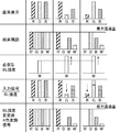
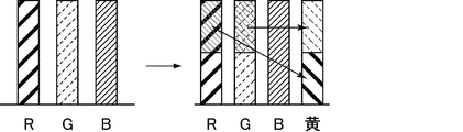
- the conventional liquid crystal display device having a multi-primary color panel has room for improvement in the following points. 40 to 43, for example, red (R) picture element (color filter), green (G) picture element (color filter) and blue (B) picture element (color filter)
- red (R) picture element (color filter) for example, red (R) picture element (color filter), green (G) picture element (color filter) and blue (B) picture element (color filter)
- RGB red
- G green
- B blue
- a normal video signal is a three-color signal of R, G, and B, it is necessary to convert from a three-color signal to a four-color signal.
- a white signal all RGB signals have maximum gradation
- all the picture elements are controlled to have the maximum transmittance (see the left side of FIG. 40). This is for maximizing the light use efficiency during white display where light must be emitted most strongly.
- yellow is added as the fourth picture element. The yellow picture element emits red and green light.
- all pixels are set to maximum transmittance, so red light is emitted from R and Y pixels, and green light is emitted from G and Y pixels (see FIG. 40 right side).
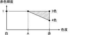
- a red signal (the R signal has the maximum gradation and the GB signal has the minimum gradation) is input. That is, the R picture element is set to the maximum gradation, and the G picture element and the B picture element are set to the minimum gradation.
- a display defect occurs due to a decrease in the luminance of red, and this defect affects a decrease in the maximum luminance at all chromaticity points.
- the picture element related to the amount of red light emitted is the R picture element when the red signal is displayed and when the white signal is displayed. Furthermore, in both cases, the R picture element is set to have the maximum transmittance. Therefore, in both cases, the amount of red light emitted does not change.
- the maximum luminance at the time of monochrome display is lowered.
- the horizontal axis is the chromaticity from the white chromaticity point to the red chromaticity point and the vertical axis is the red luminance (normalized with the maximum luminance at white as 1)
- RGB three-color filters are used.
- the red luminance when the four-color filter of RGBY is used is reduced to the extent that light does not pass through the Y picture element.
- green light is required as it approaches the white point, and therefore the transmittance of the Y picture element can be increased. Therefore, it is possible to emit red light from the Y picture element.
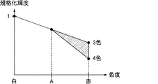
- FIG. 43 shows this as a normalized luminance value obtained by mixing all colors.
- the combination of chromaticity and luminance painted with diagonal lines can be realized with the RGB three-color filter, but cannot be realized with the RGBY four-color filter.
- red and green in the above description are changed to green and blue, and when magenta is used, all the explanations are satisfied by changing red and green to red and blue.
- the range that can be realized by a combination of chromaticity and luminance is reduced around the primary color points of red, green, and blue.
- the maximum luminance may be lowered in a chromaticity range near a single color.
- the present invention has been made in view of the above situation, and an object thereof is to provide a liquid crystal display device including a multi-primary color panel capable of improving the display quality of a single color or a color close to a single color, and a control method thereof. It is.
- the inventors of the present invention have made various studies on a liquid crystal display device including a multi-primary color panel capable of improving the display quality of a single color or a color close to a single color, and focused on a backlight driving method. Then, the backlight emission intensity is controlled according to the input image signal, and the backlight emission intensity when displaying a single color or a color close to a single color in the display area is displayed when white is displayed in the display area. It has been found that the luminance can be improved in a chromaticity range of a single color or a color close to a single color by making the emission intensity higher than the above, and the inventors have conceived that the above problems can be solved brilliantly and have reached the present invention. .
- the present invention is a liquid crystal display device that performs display by inputting image signals of three colors from the outside
- the liquid crystal display device includes a liquid crystal display panel and a backlight
- the display of the liquid crystal display panel A plurality of pixels each including four or more color pixels are formed in the region, and each pixel includes three color pixels each having a color filter corresponding to the color of the image signal, and the image And at least one picture element in which a color filter of a color corresponding to a color other than the signal color is formed, and the light emission intensity of the backlight can be controlled according to an input image signal, and the display
- the light emission intensity of the backlight when displaying a single color or a color close to a single color in the area is larger than the light emission intensity when displaying white in the display area (the light emission intensity of the backlight).
- a color close to a single color includes the single color as a component of transmitted light among at least one color pixel in which a color filter corresponding to a color other than the color of the image signal is formed. It means the color when the picture element is set to a gradation other than the highest gradation and the picture element that transmits the single color is set to the highest gradation.
- the configuration of the liquid crystal display device of the present invention is not particularly limited by other components as long as such components are formed as essential.
- the backlight has a plurality of lighting portions capable of controlling the light emission intensity independently of each other, and a color of the display area corresponding to any of the plurality of lighting portions is a single color or a color close to the single color. It is preferable that the light emission intensity of the lighting portion when displaying is larger than the light emission intensity when white is displayed in the portion (the portion having the display area). As a result, it is possible to further reduce power consumption.
- the present invention is also a liquid crystal display device that performs display by inputting image signals of three colors from the outside, and the liquid crystal display device has a liquid crystal display panel, a backlight, and a light emission intensity of the backlight.
- a backlight intensity determination circuit that determines each frame, and a plurality of pixels each including four or more picture elements are formed in the display area of the liquid crystal display panel, and each pixel is a color of the image signal 3 color picture elements each having a color filter corresponding to the color, and at least one color picture element having a color filter corresponding to a color other than the color of the image signal.
- the light emission intensity can be controlled in accordance with an input image signal, and the backlight intensity determination circuit converts the three color image signals input from the outside into signals of four or more colors corresponding to the colors of the picture elements. Conversion to A backlight light quantity calculation circuit for obtaining the minimum necessary light emission intensity of the backlight for each pixel based on the signals of four colors or more, and a maximum value for obtaining the largest light emission intensity among the minimum light emission intensity
- the backlight is a liquid crystal display device that emits light at the light emission intensity determined by the maximum value determination circuit (the highest light emission intensity).
- the gradation of the image signal output to the source driver becomes more than the maximum gradation due to insufficient light intensity of the backlight. May occur.
- the image signal of 3 colors is temporarily converted into a signal of 4 colors or more, and further, the minimum necessary light emission intensity of the backlight is obtained for each pixel based on these signals. The highest light emission intensity can be obtained from the minimum light emission intensity. Therefore, it is possible to prevent the above-described problem from occurring.
- the entire display screen is dark, the light emission intensity of the backlight can be further reduced, so that further reduction in power consumption is possible.
- the configuration of the second liquid crystal display device of the present invention is not particularly limited by other components as long as such components are essential. A preferred embodiment of the second liquid crystal display device of the present invention will be described in detail below.
- the backlight light amount calculation circuit includes a magnitude of light transmitted through a color filter (reference color filter) corresponding to a color of the image signal and a color filter (additional color filter) corresponding to a color other than the color of the image signal. ),
- the three-color image signal may be converted into a signal of four or more colors based on the magnitude of the component of the light transmitted through the reference color filter included in the light transmitted through).
- Each of the three color image signals is composed of gradation data
- the backlight intensity determination circuit performs inverse gamma conversion on the image signal composed of gradation data (three color image signals composed of the gradation data)
- the backlight has a plurality of lighting portions capable of controlling the emission intensity independently of each other, and in the maximum value determination circuit, for each portion of the display area corresponding to each lighting portion, the necessary minimum
- the backlight intensity determination circuit calculates the highest emission intensity among the emission intensity, and the backlight intensity determination circuit adds the luminance distribution on the illuminated surface of the panel when each lighting unit emits light with the minimum required emission intensity. It is preferable to further include a pattern calculation circuit. As a result, it is possible to further reduce power consumption.
- the backlight light amount calculation circuit is a first backlight light amount calculation circuit
- the maximum value determination circuit is a first maximum value determination circuit
- the backlight intensity determination circuit is the first maximum value.
- the three-color image signal is converted into a signal of four or more colors corresponding to the color of the picture element, and based on the signal of four or more colors
- a second backlight light amount calculation circuit that obtains the minimum necessary light emission intensity of the backlight for each pixel, and the largest light emission among the minimum light emission intensity calculated by the second backlight light amount calculation circuit
- the backlight may further include a second maximum value determination circuit for obtaining an intensity, and the backlight may emit light with the light emission intensity determined by the second maximum value determination circuit (the maximum light emission intensity). That is, the backlight may emit light with the light emission intensity determined by the second maximum value determination circuit instead of the light emission intensity determined by the first maximum value determination circuit. As a result, it is possible to further reduce power consumption.
- the present invention further relates to a method for controlling a liquid crystal display device that performs display by inputting image signals of three colors from the outside.
- the liquid crystal display device includes a liquid crystal display panel and a backlight, and the liquid crystal display panel In the display area, a plurality of pixels each including four or more color pixels are formed, and each pixel has three color pixels each having a color filter of a color corresponding to the color of the image signal, Including at least one color pixel in which a color filter of a color corresponding to a color other than the color of the image signal is formed, and the emission intensity of the backlight can be controlled according to the input image signal,
- the control method includes a backlight intensity determination step for determining the emission intensity of the backlight for each frame, and the backlight intensity determination step includes (1) an image signal of three colors input from the outside as a pixel.
- the backlight is also a method for controlling a liquid crystal display device that emits light with the light emission intensity determined in the step (2) (the largest light emission intensity).
- the image signal of three colors is once converted into a signal of four colors or more, and the minimum necessary light emission intensity of the backlight is obtained for each pixel based on these signals.
- the highest light emission intensity is determined from the minimum light emission intensity. For this reason, it is possible to prevent the occurrence of the problem that the above-described gradation becomes the maximum gradation or more. Further, when the entire display screen is dark, it is possible to further reduce the backlight intensity, so that it is possible to further reduce power consumption.
- the configuration of the control method of the liquid crystal display device of the present invention is not particularly limited by other components and steps as long as such components and steps are essential.
- a preferred embodiment of the liquid crystal display device control method of the present invention will be described in detail below.
- the three-color image signal may be converted into a signal of four or more colors based on the magnitude of the component of the light that passes through the reference color filter included in the light that passes through.
- Each of the three color image signals is composed of gradation data
- the backlight intensity determination step (3) performs inverse gamma conversion on the image signal composed of the gradation data (three color image signals composed of the gradation data).
- the method further includes a step of generating a three-color image signal composed of luminance data, and (4) a step of dividing the three-color image signal composed of the luminance data by the maximum light emission intensity. Thereby, it can prevent that the emitted light intensity of a backlight becomes a negative value.
- the backlight has a plurality of lighting portions capable of controlling the emission intensity independently of each other, and in the step (2), the minimum necessary amount is provided for each portion of the display area corresponding to each lighting portion.
- the backlight intensity determining step calculates the luminance distribution on the illuminated surface of the panel when each lighting section emits light at the minimum required emission intensity. It is preferable to further include the step of adding. As a result, it is possible to further reduce power consumption.
- the backlight intensity determination circuit (6) uses the light emission intensity determined in the step (2) (the largest light emission intensity) to convert the three color image signals into four or more colors corresponding to the color of the pixel. Converting to a signal, and obtaining a required minimum emission intensity of the backlight for each pixel based on the signals of four or more colors; (7) a minimum required emission intensity calculated in the step (6);
- the backlight may emit light at the light emission intensity determined in the step (7) (the highest light emission intensity). That is, the backlight may emit light with the light emission intensity determined in the step (7) instead of the light emission intensity determined in the step (2). As a result, it is possible to further reduce power consumption.
- the display quality of a single color or a color close to a single color can be improved.
- FIG. 1 is a schematic cross-sectional view illustrating a configuration of a liquid crystal display device according to Embodiment 1.
- FIG. 4 is a diagram for explaining a driving method of the liquid crystal display device of Embodiment 1.
- FIG. 6 is a schematic cross-sectional view illustrating a configuration of a liquid crystal display device of Embodiment 2.
- FIG. 6 is a schematic cross-sectional view illustrating a configuration of a liquid crystal display panel of Embodiment 2.
- FIG. 6 is a schematic plan view illustrating a pixel arrangement of a liquid crystal display device of Embodiment 2.
- FIG. 6 is a schematic plan view showing another pixel arrangement of the liquid crystal display device of Embodiment 2.
- FIG. 6 is a diagram for explaining a driving method of the liquid crystal display device of Embodiment 2.
- FIG. 6 is a block diagram showing a circuit of a liquid crystal display device of Embodiment 2.
- FIG. 10 is a diagram for explaining a backlight intensity determination algorithm in Embodiment 2.
- FIG. It is a figure which shows the block configuration of the liquid crystal display device of Embodiment 2. The flow of a process in the backlight intensity determination circuit of Embodiment 2 is shown.
- the block diagram of the backlight intensity determination circuit of Embodiment 2 is shown. 6 shows a flow of processing in a color conversion circuit of Embodiment 2.
- FIG. 3 is a block diagram of a color conversion circuit according to a second embodiment.
- FIG. 10 is a diagram for explaining a driving method of the liquid crystal display device of Embodiment 3.
- FIG. 10 is a diagram for explaining a conversion algorithm from a three-color signal to a four-color signal in the third embodiment.
- FIG. 10 is a diagram for explaining a conversion algorithm from a three-color signal to a four-color signal in the third embodiment.
- 10 is a diagram for explaining a backlight intensity determination algorithm in Embodiment 3.
- FIG. 10 shows a flow of processing in a color conversion circuit of Embodiment 3.
- FIG. 10 is a diagram for explaining a driving method of the liquid crystal display device of Embodiment 3.
- FIG. 10 is a diagram for explaining a backlight intensity determination algorithm in Embodiment 4.
- FIG. FIG. 9 is a block diagram of a backlight intensity determination circuit according to a fourth embodiment.
- 10 is a diagram for explaining a driving method of the liquid crystal display device of Embodiment 5.
- FIG. 10 is a diagram for explaining a backlight intensity determination algorithm in Embodiment 5.
- FIG. 10 is a block diagram illustrating a circuit of a liquid crystal display device according to a sixth embodiment.
- FIG. 10 is a diagram for explaining a backlight intensity determination algorithm in the sixth embodiment.
- FIG. 10 is a block diagram of a backlight intensity determination circuit according to a sixth embodiment.
- FIG. 10 is a block diagram illustrating a circuit of a liquid crystal display device according to a seventh embodiment.
- FIG. 10 is a block diagram illustrating a circuit of a liquid crystal display device according to a seventh embodiment.
- FIG. 10 is a schematic cross-sectional view illustrating a configuration of a liquid crystal display device according to an eighth embodiment.
- FIG. 10 is a schematic plan view illustrating a configuration of a backlight according to an eighth embodiment. 9 shows a processing flow in a backlight intensity determination circuit according to the eighth embodiment.
- FIG. 19 is a block diagram of a backlight intensity determination circuit according to an eighth embodiment.
- FIG. 10 is a diagram for explaining a function of a lighting pattern calculation circuit according to an eighth embodiment.
- FIG. 10 is a diagram for explaining a function of a lighting pattern calculation circuit according to an eighth embodiment.
- FIG. 19 is a block diagram illustrating another configuration of a backlight intensity determination circuit according to the eighth embodiment.
- FIG. 19 is a block diagram illustrating another configuration of a backlight intensity determination circuit according to the eighth embodiment.
- 10 is a schematic plan view illustrating a pixel arrangement of a liquid crystal display device according to Embodiment 9.
- FIG. FIG. 10 is a block diagram of a color conversion circuit according to a ninth embodiment. It is a figure for demonstrating the subject of the conventional liquid crystal display device provided with a multi-primary color panel. It is a figure for demonstrating the subject of the conventional liquid crystal display device provided with a multi-primary color panel. It is a figure for demonstrating the subject of the conventional liquid crystal display device provided with a multi-primary color panel. It is a figure for demonstrating the subject of the conventional liquid crystal display device provided with a multi-primary color panel. It is a figure for demonstrating the subject of the conventional liquid crystal display device provided with a multi-primary color panel.
- red is abbreviated as R or r
- green as G or g
- blue as B or b
- white as W or w
- yellow as Y
- cyan as C
- magenta as M.
- FIG. 1 is a schematic cross-sectional view illustrating the configuration of the liquid crystal display device according to the first embodiment.
- the liquid crystal display device according to the present embodiment includes a backlight unit (backlight 102) that can independently change the emission intensities of red, green, and blue, and a liquid crystal display panel 101 having color filters other than RGB. It is a combined transmission type liquid crystal display device.
- the liquid crystal display panel 101 When the liquid crystal display panel 101 is used, there is a problem of a decrease in luminance when a white color is displayed with a backlight and a single color is displayed. However, this can be compensated by combining the backlight 102 and the liquid crystal display panel 101 and changing the light emission intensity (lighting intensity) of the backlight 102.
- the basic driving method is -Depending on the gradation of the input signal, -Adjust the backlight emission intensity (hereinafter also referred to as backlight intensity) An output signal calculated from the emission intensity and the gradation of the input signal is sent to the liquid crystal display panel. By simply executing this driving method as it is, a decrease in monochromatic luminance occurs. A specific driving method for preventing this decrease in luminance will be described below.
- FIG. 2 is a diagram for explaining a driving method of the liquid crystal display device according to the first embodiment.
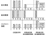
- a color filter using normal RGB and newly added yellow is used. That is, it is assumed that a Y picture element is added to an RGB three color picture element.
- the yellow color filter transmits R light and G light.
- white display when RGB signals of 255 gradations are all input, it is preferable to control all the color picture elements to 255 gradations in consideration of efficiency. At this time, the white balance needs to be balanced, but since the r light and g light are transmitted through the yellow filter, the backlight intensities of r and g are lowered accordingly (see the left column in FIG. 2). ).
- the r light intensity of the backlight is increased by the amount that the R light is insufficient.
- the intensity of the r light that is insufficient for display can be compensated (see the right column in FIG. 2). In this way, it is possible to prevent a decrease in monochromatic luminance.
- This embodiment is characterized in that control is performed so that the highest light emission intensity is not obtained when any color of the RGB backlight has 255 gradations, but the single light display.
- the liquid crystal display panel 101 having color filters of colors other than RGB when used, there is a problem that the luminance decreases when the backlight is turned on white and a single color is displayed. It is possible to prevent the liquid crystal display panel having the color filter from becoming larger than when the liquid crystal display panel is used.
- R intensity of light emitted from R picture element
- G intensity of light emitted from G picture element
- B intensity of light emitted from B picture element
- r BL backlight intensity of r g BL : back of g
- Light intensity b BL Back light intensity of b r
- R Transmittance of R light
- G Transmittance of G light
- b B Transmittance of B light
- r Y r This is the transmittance of light Y picture element, and it passes a light r times as compared with R picture element.
- g Y Transmittance of Y light element of g light, and b light of g light is transmitted as compared with G picture element.
- the light intensity of the red component transmitted through the panel is 1 / (1 + a) for all red compared to all white.
- R total white R total red
- two methods a method of changing the transmittance of the liquid crystal and a method of changing the light emission intensity of the backlight, can be considered.
- the present embodiment proposes a method for increasing the backlight intensity as compared with the case of all white. This will be described in detail in the following embodiments.
- 100% of the backlight intensity is based on the backlight intensity when displaying all white.
- FIG. 3 is a schematic cross-sectional view illustrating the configuration of the liquid crystal display device according to the second embodiment.
- the liquid crystal display device according to the present embodiment includes a white backlight unit (backlight 202) capable of changing emission intensity, a color filter of three primary colors of RGB, and a color filter of primary colors other than RGB. Is a transmissive liquid crystal display device.
- the light emission intensity of the backlight 202 is uniformly controlled (changed) over the entire light emitting surface.
- the white backlight here refers to the display color when the gradation of all color filters (picture elements) is set to the maximum gradation when combined with a liquid crystal display panel having color filters (picture elements) of RGB and other colors. Is the ideal backlight for white. By finely adjusting the white balance, white display may be performed where all the color filters (picture elements) are not at the maximum gradation.
- the light source of the white backlight is not particularly limited, and may be a cold cathode fluorescent lamp (CCFL), a white LED, or RGB three types of light emitting diodes (LED).
- a yellow color filter (Y picture element) is added, but when a cyan color filter (C picture element) is added, R is added to B and a magenta color filter (M picture element) is added.
- Y picture element a yellow color filter
- C picture element cyan color filter
- M picture element a magenta color filter
- FIG. 4 shows the configuration of the liquid crystal display panel of the second embodiment.
- FIG. 5 shows a pixel arrangement of the liquid crystal display device according to the second embodiment.
- FIG. 6 shows another pixel arrangement of the liquid crystal display device according to the second embodiment.
- the liquid crystal display panel 201 includes a pair of transparent substrates 2 and 3, a liquid crystal layer 4 sealed in a gap between the substrates 2 and 3, and one of the substrates 2 and 3, for example, an observation side (upper side in the drawing).
- the liquid crystal display panel 201 is an active matrix liquid crystal display element having TFTs (thin film transistors) as active elements. Although omitted in FIG. 4, a plurality of TFTs disposed on the inner surface of the substrate 2 on which the pixel electrodes 5 are formed are arranged in correspondence with the pixel electrodes 5, respectively connected to the pixel electrodes 5, and each row. A plurality of scanning lines for supplying gate signals to the TFTs and a plurality of data lines for supplying data signals to the TFTs in each column are provided.
- TFTs thin film transistors
- the liquid crystal display panel 201 displays an image by controlling the transmission of light emitted from the backlight 202 disposed on the opposite side to the observation side.
- the liquid crystal display panel 201 has a plurality of pixels 14.
- a data signal is supplied to a region where the pixel electrode 5 and the counter electrode 6 are opposed to each other, that is, a voltage corresponding to the data signal is applied between the electrodes 5 and 6, whereby the liquid crystal layer 4 changes the alignment state of the liquid crystal molecules, and as a result, the transmission of light is controlled.
- each pixel 14 includes an R picture element 13R including a red color filter 7R and a green color filter 7G as illustrated in FIG.
- a G picture element 13G, a B picture element 13B including a blue color filter 7B, and a Y picture element 13Y including a yellow color filter 7Y are included.
- the arrangement of the four color picture elements may be an arrangement of 2 picture elements ⁇ 2 picture elements, a stripe arrangement as shown in FIG. 6, or a mosaic type arrangement (not shown) Alternatively, delta type arrays can also be used.
- the color filters 7 ⁇ / b> R, 7 ⁇ / b> G, 7 ⁇ / b> B, and 7 ⁇ / b> Y are formed on one of the substrates 2 and 3, for example, the inner surface of the observation side substrate 3.
- the counter electrode 6 is formed on the color filters 7R, 7G, 7B, and 7Y, and the inner surfaces of the substrates 2 and 3 cover the pixel electrode 5 and the counter electrode 6, respectively, and the alignment film 9, 10 is provided.
- the substrates 2 and 3 are opposed to each other with a predetermined gap, and the pixels 14 are joined by a frame-shaped sealing material (not shown) surrounding the display region arranged in a matrix.
- a liquid crystal layer 4 is enclosed in a region surrounded by the sealing material between the substrates 2 and 3.
- the liquid crystal display panel 201 is a TN or STN type in which the liquid crystal molecules of the liquid crystal layer 4 are twist aligned, a vertical alignment type in which the liquid crystal molecules are aligned substantially perpendicular to the surfaces of the substrates 2 and 3, and the liquid crystal molecules are twisted. Without any horizontal alignment type that is aligned substantially parallel to the surfaces of the substrates 2 and 3, bend alignment type that bends liquid crystal molecules, or a ferroelectric or antiferroelectric liquid crystal display element.
- the polarizing plates 11 and 12 are arranged such that the direction of each transmission axis is set so that the display when the voltage is not applied between the electrodes 5 and 6 of each pixel 14 is black.
- the liquid crystal display panel 201 shown in FIG. 4 changes the alignment state of liquid crystal molecules by generating an electric field between the electrodes 5 and 6 provided on the inner surfaces of the pair of substrates 2 and 3, respectively.
- the electrodes 5 and 6 provided on the inner surfaces of the pair of substrates 2 and 3, respectively.
- comb-like first and second electrodes for forming a plurality of pixels are provided on the inner surface of one of the pair of substrates, and a horizontal electric field (direction along the substrate surface) is provided between these electrodes.
- a lateral electric field control type in which the alignment state of the liquid crystal molecules is changed by generating an electric field).
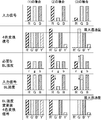
- FIG. 7 is a diagram for explaining a driving method of the liquid crystal display device according to the second embodiment.
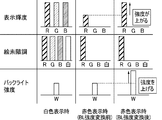
- the relationship between the backlight intensity and the pixel gradation when white is displayed with the maximum gradation is as shown in the left column of FIG. Each color picture element has the maximum gradation.
- red is displayed with the maximum gradation without changing the light emission intensity of the backlight (see the middle column in FIG. 7).
- R has the maximum gradation, and all other picture elements are controlled to 0 gradation.
- the display is displayed in red, but this red luminance is darker than that in white display.
- the red luminance when displaying white is a combination of the red light transmitted through the R filter and the red light transmitted through the yellow filter, whereas the red luminance when displaying red is transmitted through the R filter. It is to become only red light.
- control is performed to increase the light emission intensity of the backlight (see the right column in FIG. 7). Assuming that the amount of red light transmitted from the yellow filter during white display is ⁇ times the amount of red light transmitted from the R filter, the red luminance in the middle column is 1 / ( 1 + ⁇ ) times.
- the light emission intensity of the backlight may be multiplied by (1 + ⁇ ).
- the control procedure is (1) The minimum required backlight intensity is extracted for all pixels, and the largest backlight intensity is calculated from the extracted backlight intensity.
- the gradation to be input to each color picture element is calculated with respect to the calculated backlight intensity. It becomes.
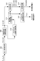
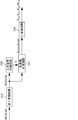
- FIG. 1 A system block diagram for realizing the above system is shown in FIG.
- the input signal is input to the backlight intensity determination circuit. With this circuit, the minimum backlight intensity required for display is determined according to the input signal.
- the obtained backlight intensity is transmitted to the backlight as a backlight intensity signal.
- the input signal is converted into a signal corresponding to the changed backlight intensity, input to a color conversion circuit (three-color four-color conversion circuit), and converted into a four-color signal.
- An image can be output by inputting a backlight intensity signal to a circuit for controlling the backlight (backlight driving circuit) and inputting four-color signals to a circuit for controlling the panel (source driver).
- R ′ (1 + ⁇ ) ⁇ R ⁇ ⁇ MAX (R, G) (c)
- G ′ (1 + ⁇ ) ⁇ G ⁇ ⁇ MAX (R, G) (d) It becomes.
- R ′ and G ′ need to satisfy 0 ⁇ R ′ ⁇ 1 and 0 ⁇ G ′ ⁇ 1, respectively. It is possible to make the value less than 1 by increasing the backlight intensity, but it is impossible to avoid taking a negative value by adjusting the backlight intensity. There is. There are three ways of dividing: (1) (c), (d) both take positive values, (2) (c) take negative values, (3) (d) take negative values. It is.
- FIG. 9 is a diagram for explaining a backlight intensity determination algorithm according to the second embodiment.
- the backlight intensity required for each pixel is obtained, and the maximum value is set to the backlight intensity necessary for display.
- a method for obtaining the required backlight intensity w for each pixel will be described.
- w takes an intensity value of 1 when the values of the input signals RGB are all 1 and R′G′B′Y ′ is converted to 1.
- the value converted into the R′G′B′Y ′ signal is as follows.
- B ' B (common in all cases)
- Conditions (1) to (3) listed here are as follows.
- the maximum value in the case of (1) is MAX (R, G, B)
- the maximum value in the case of (2) is B or (1 + ⁇ ) ⁇ G ⁇ ⁇ (1 + ⁇ ) / ⁇ ⁇ R, (3 ) Is B or (1 + ⁇ ) ⁇ R ⁇ ⁇ (1 + ⁇ ) / ⁇ ⁇ G
- the backlight intensity w required for a pixel of a combination of input signals RGB is R, G, B (1 + ⁇ ) ⁇ G ⁇ ⁇ (1 + ⁇ ) / ⁇ ⁇ R (1 + ⁇ ) ⁇ R ⁇ ⁇ (1 + ⁇ ) / ⁇ ⁇ G
- the backlight intensity required for the entire backlight unit is obtained for all combinations of the input signals RGB described above. It becomes the maximum value among the maximum values of the five values.
- the minimum backlight intensity required for each pixel is determined. Then, the input signal RGB is divided by the necessary backlight intensity w obtained here. (Refer to the fourth stage from the top in FIG. 9) Then, the divided input signal RGB is converted into a four-color signal. (Refer to the fifth stage from the top in FIG. 9) Therefore, even if the output gradation becomes equal to or greater than the maximum gradation when the input signal is converted into four colors as it is (see the second stage from the top in FIG. 9), R The values of 'G'B'Y' are all numbers from 0 to 1.
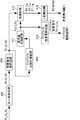
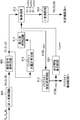
- FIG. 10 illustrates a block configuration of the liquid crystal display device according to the second embodiment.
- a driving circuit for driving the liquid crystal display panel 201 to display an image includes a source driver 206 that supplies a data voltage based on the image signal to each pixel electrode in the liquid crystal display panel 201, The gate driver 207 that drives each pixel electrode in the liquid display panel 201 line-sequentially along the scanning line, the backlight intensity determination circuit 203, the color conversion circuit 204, and the maximum determined by the backlight intensity determination circuit 203 And a backlight driving circuit 205 that controls the lighting operation of the backlight 202 with the luminance L MAX .
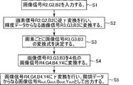
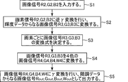
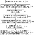
- FIG. 11 shows the flow of processing in the backlight intensity determination circuit of the second embodiment.
- the backlight intensity determination circuit 203 performs the following processing for each frame. First, RGB image (video) signals R in , G in , B in comprising gradation data are input (S1).
- one maximum luminance L MAX is obtained from the backlight light quantity L obtained for each pixel (S4).
- the image signals R1, G1, and B1 are divided by the maximum luminance L MAX for each pixel to calculate image signals R1 / L MAX , G1 / L MAX , and B1 / L MAX (S5).
- FIG. 12 is a block diagram of the backlight intensity determination circuit according to the second embodiment.
- the backlight intensity determination circuit 203 includes an inverse gamma conversion circuit 208, a luminance signal holding circuit 209, a backlight light quantity calculation circuit 210, a maximum value determination circuit 211, a division circuit 212, a backlight circuit, A light intensity holding circuit 213 and a gamma conversion circuit 214 are provided.
- the inverse gamma conversion circuit 208 performs inverse gamma conversion on the image signals R in , G in , and B in to generate image signals R 1, G 1, and B 1 including luminance data.
- the image signals R1, G1, and B1 are output to the luminance signal holding circuit 209 and stored for a certain period (for example, for one frame).
- the backlight light amount calculation circuit 210 calculates the necessary backlight light amount L for each pixel as described above.
- the backlight light quantity L is expressed by five luminances R, G, B, (1 + ⁇ ) ⁇ G ⁇ ⁇ (1 + ⁇ ) / ⁇ ⁇ R and (1 + ⁇ ) ⁇ R ⁇ ⁇ (1 + ⁇ ) / One of ⁇ ⁇ G.
- the maximum value determination circuit 211 determines one of the largest luminances L MAX from the backlight light amount L of each pixel output from the backlight light amount calculation circuit 210.
- the backlight intensity holding circuit 213 stores the maximum luminance L MAX output from the maximum value determination circuit 211 for a certain period (for example, for one frame) and outputs the maximum luminance L MAX to the backlight driving circuit 205.
- the division circuit 212 divides the image signals R1, G1, and B1 output from the luminance signal holding circuit 209 by the maximum luminance L MAX for each pixel, and outputs the image signals R1 / L MAX , G1 / L MAX , and B1 / L MAX . calculate.
- the gamma conversion circuit 214 performs gamma conversion on the image signals R1 / L MAX , G1 / L MAX , and B1 / L MAX output from the division circuit 212, and generates image signals R2, G2, and B2 including gradation data. At the same time, it is output to the color conversion circuit 204.
- FIG. 13 shows the flow of processing in the color conversion circuit of the second embodiment.
- the color conversion circuit 204 performs the following processing for each frame. First, RGB image signals R2, G2, and B2 composed of gradation data are input from the backlight intensity determination circuit 203 (S1).
- the three-color image signals R3, G3, and B3 are converted into four-color image signals R4, G4, B4, and Y4 for each pixel by the determined conversion formula (S4).
- FIG. 14 is a block diagram of the color conversion circuit according to the second embodiment.
- the color conversion circuit 204 includes an inverse gamma conversion circuit 215, an input signal determination circuit 216, a color conversion calculation circuit 217, and a gamma conversion circuit 218.
- the inverse gamma conversion circuit 215 performs inverse gamma conversion on the image signals R2, G2, and B2, and generates image signals R3, G3, and B3 including luminance data.
- the color conversion calculation circuit 217 converts the three-color image signals R3, G3, and B3 into the four-color image signals R4, G4 according to any one of the conversion formulas determined by the control signal D output from the input signal determination circuit 216. , B4, and Y4.
- Gamma conversion circuit 218 performs gamma conversion to the color conversion calculation circuit 217 image signals R4 output from, G4, B4, Y4, image signal consisting of tone data R out, G out, B out , generates a Y out And output to the source driver.
- the emission intensity of the backlight when displaying a single color or a color close to a single color is made larger than the emission intensity when displaying white, the brightness of the screen is reduced when displaying the vicinity of a single color. Can be suppressed.
- the light emission intensity of the backlight is controlled in accordance with the input image signal, so that an increase in power consumption can be suppressed.
- the liquid crystal display device of the present embodiment has the same configuration as that of the second embodiment except that a white picture element not provided with a color filter is provided instead of the yellow color filter (Y picture element).
- the thickness of the liquid crystal layer of each white pixel is approximately the same as the thickness of the liquid crystal layer of the three pixels 13R, 13G, and 13B of red, green, and blue corresponding to the white pixels.
- a colorless transparent film is prepared for adjustment.
- FIG. 15 is a diagram for explaining a driving method of the liquid crystal display device according to the third embodiment.
- the relationship between the backlight intensity and the pixel gradation when white is displayed with the maximum gradation is as shown in the left column of FIG. Each color picture element has the maximum gradation.
- red is displayed with the maximum gradation without changing the light emission intensity of the backlight (see the middle column in FIG. 15).
- R has the maximum gradation, and all other picture elements are controlled to 0 gradation.
- the display is displayed in red, but this red luminance is darker than that in white display.
- the red luminance during white display is a combination of the red light transmitted through the R filter and the red light transmitted through the white filter, whereas the red luminance during red display is transmitted through the R filter. It is to become only red light.
- control is performed to increase the light emission intensity of the backlight (see the right column in FIG. 15). Assuming that the amount of red light transmitted from the white filter during white display is ⁇ times the amount of red light transmitted from the R filter, the red luminance in the middle column is 1 / ( 1 + ⁇ ) times.
- the light emission intensity of the backlight may be multiplied by (1 + ⁇ ).
- the control procedure is (1) The minimum required backlight intensity is extracted for all pixels, and the largest backlight intensity is calculated from the extracted backlight intensity.
- the gradation to be input to each color picture element is calculated with respect to the calculated backlight intensity. It becomes.
- the system block for realizing the above-described system is the same as that shown in FIG. 8 of the second embodiment, and the flow of generating a four-color signal from the input signal is the same.
- the algorithm for determining the backlight intensity is different and will be described below.
- 16 and 17 are diagrams for explaining a conversion algorithm from a three-color signal to a four-color signal in the third embodiment.
- An algorithm for converting RGB input signals to R′G′B′W ′ is shown.
- the transmission amount of red light from the white filter is ⁇ times the transmission amount from the red filter.
- the transmission amount of green light from the white filter is ⁇ times the transmission amount from the green filter.
- the transmission amount of blue light from the white filter is ⁇ times the transmission amount from the blue filter.
- all the numbers of R ′, G ′, and B ′ must be 0 or more, but may take a negative number depending on the value of the input signal. In this case, it is necessary to change the value including W ′.
- the number of all R ′, G ′, and B ′ is 0 or more, it is as shown in the left column of FIG.
- FIG. 18 is a diagram for explaining a backlight intensity determination algorithm according to the third embodiment.
- the backlight intensity required for each pixel is obtained, and the maximum value is set to the backlight intensity necessary for display.
- a method for obtaining the required backlight intensity w for each pixel will be described.
- w takes an intensity value of 1 when all the values of the input signal RGB are 1 and R′G′B′W ′ is converted to 1.
- the following nine values may have the maximum value.
- R, G, B (1 + ⁇ ) ⁇ R ⁇ ⁇ (1 + ⁇ ) / ⁇ ⁇ G (1 + ⁇ ) ⁇ G ⁇ ⁇ (1 + ⁇ ) / ⁇ ⁇ R (1 + ⁇ ) ⁇ R ⁇ ⁇ (1 + ⁇ ) / ⁇ ⁇ B (1 + ⁇ ) ⁇ B ⁇ ⁇ (1 + ⁇ ) / ⁇ ⁇ R (1 + ⁇ ) ⁇ B ⁇ ⁇ (1 + ⁇ ) / ⁇ ⁇ G (1 + ⁇ ) / ⁇ ⁇ B
- the backlight intensity required for a pixel of a combination of certain input signals RGB is the maximum of the above nine values.
- the backlight intensity required for the entire backlight unit is obtained for all combinations of the input signals RGB described above. It becomes the maximum value among the maximum values of the nine values.
- the minimum backlight intensity required for each pixel is determined. Then, the input signal RGB is divided by the necessary backlight intensity w obtained here. (Refer to the fourth stage from the top in FIG. 18.) Then, the divided input signal RGB is converted into a four-color signal. (Refer to the fifth stage from the top in FIG. 18) Therefore, even if the output gradation is equal to or higher than the maximum gradation when the input signal is converted into four colors as it is (see the second stage from the top in FIG. 18), R The values of 'G'B'W' are all numbers of 1 or less. As described above, the value of R'G'B'W 'is 1 or less by controlling the backlight intensity, and the value of R'G'B'W' is 0 or more depending on the case of conversion from 3 colors to 4 colors. become.
- the liquid crystal display device of this embodiment has the same block configuration as that of the second embodiment shown in FIG.
- the backlight intensity determination circuit of the present embodiment performs the same processing as that of the second embodiment shown in FIG.
- the backlight intensity determination circuit of the present embodiment has the same block configuration as that of the second embodiment shown in FIG.
- the backlight light amount L required for each pixel is nine luminances R, G, B, (1 + ⁇ ) ⁇ R ⁇ ⁇ (1 + ⁇ ) / ⁇ ⁇ G, (1 + ⁇ ) ⁇ , as described above.
- FIG. 19 shows the flow of processing in the color conversion circuit of the third embodiment.
- the following processing is performed for each frame.
- RGB image signals R2, G2, and B2 composed of gradation data are input from the backlight intensity determination circuit (S1).
- the three-color image signals R3, G3, and B3 are converted into four-color image signals R4, G4, B4, and W4 for each pixel by the determined conversion formula (S4).
- FIG. 20 is a block diagram of a color conversion circuit according to the third embodiment.
- the color conversion circuit of this embodiment includes an inverse gamma conversion circuit 315, an input signal determination circuit 316, a color conversion calculation circuit 317, and a gamma conversion circuit 318.
- the inverse gamma conversion circuit 315 performs inverse gamma conversion on the image signals R2, G2, and B2, and generates image signals R3, G3, and B3 including luminance data.
- the color conversion calculation circuit 317 converts the three-color image signals R3, G3, and B3 into the four-color image signals R4, G4 according to any one of the conversion formulas determined by the control signal D output from the input signal determination circuit 316. , B4, W4.
- Gamma conversion circuit 318 performs gamma conversion on the image signals R4, G4, B4, W4 outputted from the color conversion calculation circuit 317, the image signals R out consisting of gray level data, G out, B out, generates a W out And output to the source driver.
- the emission intensity of the backlight when displaying a single color or a color close to a single color is made larger than the emission intensity when displaying white, the brightness of the screen is reduced when displaying the vicinity of a single color. Can be suppressed.
- the light emission intensity of the backlight is controlled in accordance with the input image signal, so that an increase in power consumption can be suppressed.
- the liquid crystal display device of the present embodiment has the same configuration as that of the second embodiment except that an RGB backlight unit capable of independently changing the RGB emission intensity is provided instead of the white backlight unit.
- the backlight light source may be three types of RGB LEDs, but any light source may be used as long as it is a unit capable of independently adjusting the emission intensity of each of RGB.
- a yellow color filter (Y picture element) is added, but when a cyan color filter (C picture element) is added, R is added to B and a magenta color filter (M picture element) is added.
- Y picture element a yellow color filter
- C picture element cyan color filter
- M picture element a magenta color filter
- FIG. 21 is a diagram for explaining a driving method of the liquid crystal display device according to the fourth embodiment.
- the relationship between the backlight intensity and the pixel gradation when displaying white at the maximum gradation is as shown in the left column of FIG.
- the light use efficiency is maximized by setting each color picture element to the maximum gradation.
- red is displayed with the maximum gradation without changing the light emission intensity of the backlight (see the middle column in FIG. 21).
- R has the maximum gradation, and all other picture elements are controlled to 0 gradation.
- the display is displayed in red, but this red luminance is darker than that in white display.
- the red luminance when displaying white is a combination of the red light transmitted through the R filter and the red light transmitted through the yellow filter, whereas the red luminance when displaying red is transmitted through the R filter. It is to become only red light.
- control is performed to increase the emission intensity of only the red light source (see the right column in FIG. 21). Assuming that the amount of red light transmitted from the yellow filter during white display is ⁇ times the amount of red light transmitted from the R filter, the red luminance in the middle column is 1 / ( 1 + ⁇ ) times.
- the emission intensity of the red light source may be multiplied by (1 + ⁇ ).
- the control procedure is (1) The minimum required backlight intensity for all pixels is extracted for each of RGB, and the largest backlight intensity is calculated for each of RGB. (2) The gradation to be input to each color picture element is calculated with respect to the calculated backlight intensity. It becomes.
- the system block for realizing the above-described system is the same as that shown in FIG. 8 of the second embodiment, and the flow of generating a four-color signal from the input signal is the same.
- the algorithm for converting the RGB input signal input to the color conversion circuit into the R′G′B′Y ′ signal is the same as that in the second embodiment.
- FIG. 22 is a diagram for explaining a backlight intensity determination algorithm according to the fourth embodiment.
- the backlight intensity is indicated by r, g, and b.
- the original input signal Before being input to the color conversion circuit, the original input signal is converted into one divided by the backlight intensity. Therefore, the signal R′G′B′Y ′ converted into the four colors with respect to the original input signal RGB has the following relationship.
- R′G′B′Y ′ must be 0 or more and 1 or less. Since there is a restriction that does not take a negative number in conversion from three colors to four colors, rgb may be set so as to satisfy the condition that all of R′G′B′Y ′ are 1 or less.
- the minimum required backlight intensity for that pixel is the larger value of r: R and ⁇ ⁇ (1 + ⁇ ) ⁇ R / ( ⁇ + ⁇ ⁇ G).
- g The larger value of G and ⁇ ⁇ (1 + ⁇ ) ⁇ G / ( ⁇ + ⁇ ⁇ R) b: B It becomes.
- the backlight intensity required for the entire backlight unit can be obtained.
- the minimum necessary backlight intensity rgb is determined for each pixel. Then, the input signal RGB is divided by the necessary backlight intensity rgb obtained here. (Refer to the fourth stage from the top in FIG. 22) Then, the divided input signal RGB is converted into a four-color signal. (Refer to the fifth stage from the top in FIG. 22) Therefore, even if the output gradation becomes equal to or greater than the maximum gradation when the input signal is converted into four colors as it is (see the second stage from the top in FIG. 22), R The values of 'G'B'Y' are all numbers from 0 to 1.
- the necessary backlight intensity in a certain pixel is only increased for a pixel that exceeds the maximum transmission amount.
- the case of (2) will be described. This is a change assuming that the intensity of g required for other pixels is 1. If the intensity of g can be lowered even if the influence of other pixels is taken into consideration, the value of G of the input signal / BL intensity will increase, and it is necessary to further increase the intensity of g in other pixels. If there is, the value G of the input signal / BL intensity will decrease.
- the liquid crystal display device of this embodiment has the same block configuration as that of the second embodiment shown in FIG.
- the backlight intensity determination circuit of the present embodiment performs the same processing as that of the second embodiment shown in FIG.
- the required backlight light amounts L (R), L (G), and L (B) are obtained for the light sources of RGB colors.
- one maximum luminance LR of the R light source is obtained from the backlight light amount L (R) obtained for each pixel
- the G light source is obtained from the backlight light amount L (G) obtained for each pixel.
- an image signal R1 image signals R1 / L R is calculated by dividing the maximum brightness L R for each pixel, the image signal by dividing the maximum brightness L G image signal G1 for each pixel G1 / L G, and calculates an image signal B1 / L B by dividing the maximum luminance L B image signals B1 for each pixel.
- the image signal R1 / L R performs gamma conversion on the G1 / L G, B1 / L B, and outputs an image signal R2, G2, B2 consisting tone data, data for controlling the backlight
- the light amounts L R , L G , and L B are output as follows.
- FIG. 23 is a block diagram of a backlight intensity determination circuit according to the fourth embodiment.
- the backlight intensity determination circuit according to the fourth embodiment includes an inverse gamma conversion circuit 408, a luminance signal holding circuit 409, a backlight light quantity calculation circuit 410, a maximum value determination circuit 411, and a division circuit 412. And a backlight intensity holding circuit 413 and a gamma conversion circuit 414.
- the inverse gamma conversion circuit 408 performs inverse gamma conversion on the image signals R in , G in , and B in to generate image signals R 1, G 1, and B 1 including luminance data.
- the image signals R1, G1, and B1 are output to the luminance signal holding circuit 409 and stored for a certain period (for example, for one frame).
- the backlight light quantity calculation circuit 410 is based on the image signals R1, G1, and B1 output from the luminance signal holding circuit 409, and as described above, the backlight light quantity L (R), L (G), L (B) is calculated.
- the backlight light amount L (R) is a larger value of R and ⁇ ⁇ (1 + ⁇ ) ⁇ R / ( ⁇ + ⁇ ⁇ G), and the backlight light amount L (G) is G and The larger value of ⁇ ⁇ (1 + ⁇ ) ⁇ G / ( ⁇ + ⁇ ⁇ R) is obtained, and the backlight light quantity L (B) is B.
- the maximum value determination circuit 411 determines one of the most significant brightness L R from the backlight quantity calculating circuit of each pixel output from 410 backlight quantity L of (R), also from backlight quantity calculating circuit 410 determining one greatest brightness L G from the outputted backlight quantity L of each pixel (G), further, backlight quantity calculating circuit of each pixel output from 410 backlight quantity L of (B) One of the largest luminances L B is determined from the inside.
- the maximum value determination circuit 411 the maximum luminance L R output from, L G, the predetermined period L B (e.g., one frame), as well as storage, the maximum luminance L R, L G, and it outputs the L B to the backlight driving circuit.
- the division circuit 412 divides the image signals R1, G1, and B1 output from the luminance signal holding circuit 409 by the maximum luminances L R , L G , and L B for each pixel, and the image signals R1 / L R , G1 / L G , B1 / L B is calculated.
- Gamma conversion circuit 414 an image signal R1 / L R outputted from the division circuit 412 performs gamma conversion on the G1 / L G, B1 / L B, and generates an image signal R2, G2, B2 consisting gradation data At the same time, it is output to the color conversion circuit.
- the color conversion circuit of the present embodiment has the same block configuration as that of the second embodiment shown in FIG.
- the processing performed by the color conversion circuit of the present embodiment is the same as that of the second embodiment.
- the emission intensity of the backlight when displaying a single color or a color close to a single color is made larger than the emission intensity when displaying white, the brightness of the screen is reduced when displaying the vicinity of a single color. Can be suppressed.
- the light emission intensity of the backlight is controlled in accordance with the input image signal, so that an increase in power consumption can be suppressed.
- the liquid crystal display device of the present embodiment has the same configuration as that of the third embodiment except that an RGB backlight unit capable of changing the RGB emission intensity is provided instead of the white backlight unit.
- the backlight light source may be three types of RGB LEDs, but any light source may be used as long as it is a unit capable of independently adjusting the emission intensity of each of RGB.
- FIG. 24 is a diagram for explaining a driving method of the liquid crystal display device according to the fifth embodiment.
- the relationship between the backlight intensity and the pixel gradation when white is displayed at the maximum gradation is as shown in the left column of FIG.
- the light use efficiency is maximized by setting each color picture element to the maximum gradation.
- red is displayed with the maximum gradation without changing the light emission intensity of the backlight (see the middle column in FIG. 24).
- R has the maximum gradation, and all other picture elements are controlled to 0 gradation.
- the display is displayed in red, but this red luminance is darker than that in white display.
- the red luminance during white display is a combination of the red light transmitted through the R filter and the red light transmitted through the white filter, whereas the red luminance during red display is transmitted through the R filter. It is to become only red light.
- control is performed to increase the emission intensity of only the red light source (see the right column in FIG. 24). Assuming that the amount of red light transmitted from the white filter during white display is ⁇ times the amount of red light transmitted from the R filter, the red luminance in the middle column is 1 / ( 1 + ⁇ ) times.
- the intensity of the red light source may be multiplied by (1 + ⁇ ) in order to make the red luminance equal when displaying white with the maximum gradation and when displaying red with the maximum gradation.
- the entire surface is displayed with the same gradation.
- the backlight irradiation intensity is the same for all pixels. Therefore, the control procedure is (1) The minimum required backlight intensity for all pixels is extracted for each of RGB, and the largest backlight intensity is calculated for each of RGB. (2) The gradation to be input to each color picture element is calculated with respect to the calculated backlight intensity. It becomes.
- the system block for realizing the above-described system is the same as that shown in FIG. 8 of the second embodiment, and the flow of generating a four-color signal from the input signal is the same.
- FIG. 25 is a diagram for explaining a backlight intensity determination algorithm according to the fifth embodiment.
- the backlight intensity is indicated by r, g, and b.
- the original input signal Before being input to the color conversion circuit, the original input signal is converted into one divided by the backlight intensity. For this reason, the signal R′G′B′W ′ converted into four colors with respect to the original input signal RGB has the following relationship.
- R′G′B′W ′ must be 0 or more and 1 or less. Since there is a restriction that does not take a negative number in the conversion from three colors to four colors, rgb may be set so as to satisfy the condition that all of R′G′B′W ′ are 1 or less.
- the backlight intensity rgb required for a certain input signal RGB is r: Maximum value of R, ⁇ ⁇ (1 + ⁇ ) ⁇ R / ( ⁇ + ⁇ ⁇ G) ⁇ , ⁇ ⁇ (1 + ⁇ ) ⁇ R / ( ⁇ + ⁇ ⁇ B) ⁇ g: G, ⁇ ⁇ (1 + ⁇ ) ⁇ G / ( ⁇ + ⁇ ⁇ R) ⁇ , ⁇ ⁇ (1 + ⁇ ) ⁇ G / ( ⁇ + ⁇ ⁇ B) ⁇ , maximum value b: B, ⁇ ⁇ (1 + ⁇ ) ⁇ B / ( ⁇ + ⁇ ⁇ R) ⁇ , ⁇ It becomes the maximum value among x (1 + ⁇ ) ⁇ B / ( ⁇ + ⁇ ⁇ G) ⁇ .
- the backlight intensity required for the entire backlight unit can be obtained.
- the minimum necessary backlight intensity rgb is determined for each pixel. Then, the input signal RGB is divided by the required backlight intensity rgb obtained here. (Refer to the fourth stage from the top in FIG. 25) Then, the divided input signal RGB is converted into a four-color signal. (Refer to the fifth stage from the top in FIG. 25) Therefore, even if the output gradation becomes equal to or higher than the maximum gradation when the input signal is converted into four colors as it is (see the second stage from the top in FIG. 25), R The values of 'G'B'W' are all numbers of 1 or less. As described above, the value of R'G'B'W 'is 1 or less by controlling the backlight intensity, and the value of R'G'B'W' is 0 or more depending on the case of conversion from 3 colors to 4 colors. become.
- the liquid crystal display device of this embodiment has the same block configuration as that of the second embodiment shown in FIG.
- the backlight intensity determination circuit of the present embodiment performs the same processing as that of the second embodiment shown in FIG.
- the required backlight light amounts L (R), L (G), and L (B) are obtained for the light sources of RGB colors.
- one maximum luminance LR of the R light source is obtained from the backlight light amount L (R) obtained for each pixel
- the G light source is obtained from the backlight light amount L (G) obtained for each pixel.
- an image signal R1 image signals R1 / L R is calculated by dividing the maximum brightness L R for each pixel, the image signal by dividing the maximum brightness L G image signal G1 for each pixel G1 / L G, and calculates an image signal B1 / L B by dividing the maximum luminance L B image signals B1 for each pixel.
- the image signal R1 / L R performs gamma conversion on the G1 / L G, B1 / L B, and outputs an image signal R2, G2, B2 consisting tone data, data for controlling the backlight
- the light amounts L R , L G , and L B are output as follows.
- the backlight intensity determination circuit of the present embodiment has the same block configuration as that of the fourth embodiment shown in FIG.
- the backlight light amount L (R) required for each pixel is R, ⁇ ⁇ (1 + ⁇ ) ⁇ R / ( ⁇ + ⁇ ⁇ G) ⁇ , ⁇ ⁇ (1 + ⁇ ) ⁇ R / ( ⁇ + ⁇ ⁇ B) ⁇ is the maximum value
- the backlight light amount L (G) required for each pixel is G, ⁇ ⁇ (1 + ⁇ ) ⁇ G / ( ⁇ + ⁇ ⁇ R) ⁇ , ⁇ ⁇ (1 + ⁇ ) ⁇ G / ( ⁇ + ⁇ ⁇ B) ⁇
- the amount of backlight L (B) required for each pixel is B, ⁇ ⁇ (1 + ⁇ ) ⁇ B / ( ⁇ + ⁇ ⁇ R) ⁇ , ⁇ ⁇ ⁇ (1 + ⁇ ) ⁇ B / ( ⁇ + ⁇ ⁇ G) ⁇ is the maximum value.
- the color conversion circuit of the present embodiment has the same block configuration as that of the third embodiment shown in FIG.
- the processing performed by the color conversion circuit of the present embodiment is the same as that of the third embodiment.
- the emission intensity of the backlight when displaying a single color or a color close to a single color is made larger than the emission intensity when displaying white, the brightness of the screen is reduced when displaying the vicinity of a single color. Can be suppressed.
- the light emission intensity of the backlight is controlled in accordance with the input image signal, so that an increase in power consumption can be suppressed.
- the liquid crystal display device of this embodiment has the same configuration as that of the fourth embodiment. That is, an RGB backlight unit capable of independently changing the RGB emission intensity is provided.
- the backlight light source may be three types of RGB LEDs, but any light source may be used as long as it is a unit capable of independently adjusting the emission intensity of each of RGB.
- a yellow color filter (Y picture element) is added, but when a cyan color filter (C picture element) is added, R is added to B and a magenta color filter (M picture element) is added.
- Y picture element a yellow color filter
- C picture element cyan color filter
- M picture element a magenta color filter
- the intensity of g is the maximum in order to determine the intensity of r
- the intensity of r is the maximum in order to determine the intensity of g.
- the intensity of r is maximized only when there is a pixel in which the R picture element has the maximum gradation and the G picture element has the minimum gradation, which is a very limited condition.
- the intensity of g is maximized only when there is a pixel in which the G picture element has the maximum gradation and the R picture element has the minimum gradation, which is also a very limited condition.
- required in Embodiment 4 is normally higher intensity
- recalculation is performed using the value of the backlight intensity r1 obtained in the fourth embodiment in order to obtain the backlight intensity of g, and the backlight obtained in the fourth embodiment in order to obtain the backlight intensity of r.
- a method of recalculation using the value of the intensity g1 is proposed.
- the light emission intensity of the backlight can be set smaller than that in the fourth embodiment, so that further reduction in power consumption is possible.
- FIG. 26 shows a system block diagram for realizing the above system.
- input signals R, G, and B are input to the first backlight intensity determination unit, and outputs are r1, g1, and b1.
- r1, g1, and b1 are r, g, and b obtained in the fourth embodiment, respectively.
- the second backlight intensity determination unit receives input signals R, G, and B and r1, g1, and b1 output from the first backlight intensity determination unit, and outputs the backlight intensity signals r, g. , B are output to the backlight drive circuit, and signals obtained by dividing the input signals R, G, B by r, g, b are output to the color conversion circuit.
- the signal input to the color conversion circuit is converted into an R′G′B′Y ′ signal and output.
- the algorithm for converting the RGB signal input to the color conversion circuit into the R′G′B′Y ′ signal is the same as in the second and fourth embodiments.
- FIG. 27 is a diagram for explaining a backlight intensity determination algorithm according to the sixth embodiment.
- the backlight intensity is indicated by r, g, and b.
- the original input signal Before being input to the color conversion circuit, the original input signal is converted into one divided by the backlight intensity. Therefore, the signal R′G′B′Y ′ converted into the four colors with respect to the original input signal RGB has the following relationship.
- R′G′B′Y ′ must be 0 or more and 1 or less. Since there is a restriction that does not take a negative number in the conversion from three colors to four colors, rgb may be set so as to satisfy the condition that all of R′G′B′Y ′ are 1 or less.
- the minimum required backlight intensity for that pixel is the larger value of r: R and ⁇ ⁇ (1 + ⁇ ) ⁇ R / ( ⁇ + ⁇ ⁇ G).
- g The larger value of G and ⁇ ⁇ (1 + ⁇ ) ⁇ G / ( ⁇ + ⁇ ⁇ R) b: B It becomes.
- the backlight intensity required for the entire backlight unit can be obtained.
- the backlight intensity obtained here is output as r1, g1, and b1.
- the light intensity determination unit uses the output value r1 of the first backlight intensity determination unit.
- the minimum required backlight intensity for that pixel is r: R and ⁇ ⁇ (1 + ⁇ ) ⁇ g1 ⁇ / ⁇ ( ⁇ ⁇ g1 + ⁇ ⁇ (1 + ⁇ ) G ) ⁇ ⁇ R, the larger value g: G and ⁇ ⁇ (1 + ⁇ ) ⁇ r1 ⁇ / ⁇ ( ⁇ ⁇ r1 + ⁇ ⁇ (1 + ⁇ ) R) ⁇ ⁇ G, the larger value b: B It becomes.
- the backlight intensity required for the entire backlight unit can be obtained.
- the minimum necessary backlight intensity rgb is determined for each pixel. Then, the input signal RGB is divided by the necessary backlight intensity rgb obtained here. (Refer to the fourth stage from the top in FIG. 27) Then, the divided input signal RGB is converted into a four-color signal. (Refer to the fifth stage from the top in FIG. 27) Therefore, even if the output gradation becomes equal to or greater than the maximum gradation when the input signal is converted into four colors as it is (see the second stage from the top in FIG. 27), R The values of “G” B ”Y” are all numbers from 0 to 1.
- the liquid crystal display device of this embodiment has the same block configuration as that of the second embodiment shown in FIG.
- the backlight intensity determination circuit of the present embodiment performs the same processing as that of the second embodiment shown in FIG.
- the required backlight light amounts L (R), L (G), and L (B) are obtained for the light sources of RGB colors.
- one maximum luminance LR of the R light source is obtained from the backlight light amount L (R) obtained for each pixel
- the G light source is obtained from the backlight light amount L (G) obtained for each pixel.
- an image signal R1 image signals R1 / L R is calculated by dividing the maximum brightness L R for each pixel, the image signal by dividing the maximum brightness L G image signal G1 for each pixel G1 / L G, and calculates an image signal B1 / L B by dividing the maximum luminance L B image signals B1 for each pixel.
- the image signal R1 / L R performs gamma conversion on the G1 / L G, B1 / L B, and outputs an image signal R2, G2, B2 consisting tone data, data for controlling the backlight
- the light amounts L R , L G , and L B are output as follows.
- step S3 is performed a plurality of times. That is, the necessary backlight light amounts L (R), L (G), and L (B) are recalculated using the maximum luminance obtained in S4.
- FIG. 28 is a block diagram of a backlight intensity determination circuit according to the sixth embodiment.
- the backlight intensity determination circuit of the sixth embodiment includes an inverse gamma conversion circuit 608, a luminance signal holding circuit 609, backlight light quantity calculation circuits 610 and 619, maximum value determination circuits 611 and 620, and , A division circuit 612, a backlight intensity holding circuit 613, and a gamma conversion circuit 614.
- An inverse gamma conversion circuit 608 performs inverse gamma conversion on the image signals Rin, Gin, and Bin, and generates image signals R1, G1, and B1 including luminance data.
- the image signals R1, G1, and B1 are output to the luminance signal holding circuit 609 and stored for a certain period (for example, for one frame).
- the backlight light amount calculation circuit 610 is based on the image signals R1, G1, and B1 output from the luminance signal holding circuit 609, and as described above, the backlight light amount L (R), L (G), L (B) is calculated.
- the backlight light amount L (R) is a larger value of R and ⁇ ⁇ (1 + ⁇ ) ⁇ R / ( ⁇ + ⁇ ⁇ G), and the backlight light amount L (G) is G and The larger value of ⁇ ⁇ (1 + ⁇ ) ⁇ G / ( ⁇ + ⁇ ⁇ R) is obtained, and the backlight light quantity L (B) is B.
- the maximum value discriminating circuit 611 determines one largest luminance L R ′ (assumed maximum luminance value) from the backlight light amount L (R) of each pixel output from the backlight light amount calculating circuit 610, and , One of the largest luminance L G ′ (assumed maximum luminance value) is determined from the backlight light amount L (G) of each pixel output from the backlight light amount calculation circuit 610, and the backlight light amount calculation circuit One of the largest luminance L B ′ (assumed maximum luminance value) is determined from the backlight light quantity L (B) of each pixel output from 610.
- the backlight light amount calculation circuit 619 is based on the image signals R1, G1, and B1 output from the luminance signal holding circuit 609 and the luminances L R ′, L G ′, and L B ′ output from the maximum value determination circuit 611. As described above, the backlight light amounts L2 (R), L2 (G), and L2 (B) necessary for each pixel are calculated.
- the backlight light amount L2 (R) is the larger value of R and ⁇ ⁇ (1 + ⁇ ) ⁇ g1 ⁇ / ⁇ ( ⁇ ⁇ g1 + ⁇ ⁇ (1 + ⁇ ) G) ⁇ ⁇ R
- the backlight light amount L2 (G) is a larger value of G and ⁇ ⁇ (1 + ⁇ ) ⁇ r1 ⁇ / ⁇ ( ⁇ ⁇ r1 + ⁇ ⁇ (1 + ⁇ ) R) ⁇ ⁇ G
- the backlight light amount L2 (B) Becomes B.
- the maximum value determination circuit 620 determines one of the most significant brightness L R from the backlight quantity calculating circuit 619 backlight quantity of each pixel output from L2 (R), also from backlight quantity calculating circuit 619 one determines the highest brightness L G from the backlight quantity of each pixel output L2 (G), further, backlight quantity calculating circuit 619 backlight quantity of each pixel output from L2 of (B) One of the largest luminances L B is determined from the inside.
- the maximum value determination circuit 620 the maximum luminance L R output from, L G, the predetermined period L B (e.g., one frame), as well as storage, the maximum luminance L R, L G, and it outputs the L B to the backlight driving circuit.
- the division circuit 612 divides the image signals R1, G1, and B1 output from the luminance signal holding circuit 609 by the maximum luminances L R , L G , and L B for each pixel, and the image signals R1 / L R , G1 / L G , B1 / L B is calculated.
- Gamma conversion circuit 614 an image signal R1 / L R outputted from the division circuit 612 performs gamma conversion on the G1 / L G, B1 / L B, and generates an image signal R2, G2, B2 consisting gradation data At the same time, it is output to the color conversion circuit.
- the color conversion circuit of the present embodiment has the same block configuration as that of the second embodiment shown in FIG.
- the processing performed by the color conversion circuit of the present embodiment is the same as that of the second embodiment.
- the emission intensity of the backlight when displaying a single color or a color close to a single color is made larger than the emission intensity when displaying white, the brightness of the screen is reduced when displaying the vicinity of a single color. Can be suppressed.
- the light emission intensity of the backlight is controlled in accordance with the input image signal, so that an increase in power consumption can be suppressed.
- the number of times the backlight intensity is calculated is not particularly limited to two, and may be three or more.
- the number of maximum value determination circuits is not necessarily the same as the number of backlight light quantity calculation circuits, and may be smaller than the number of backlight light quantity calculation circuits, for example, one. Specifically, for example, without providing the maximum value determination circuit 620, the maximum luminance L R at the maximum value determination circuit 611, L G, it may determine the L B.
- the liquid crystal display device of this embodiment has the same configuration as that of the fifth embodiment. That is, an RGB backlight unit capable of independently changing the RGB emission intensity is provided.
- the intensity of g is the maximum in order to determine the intensity of r, or the intensity of b is the maximum, and the intensity of r is determined to determine the intensity of g.
- the case where the intensity is the maximum or the case where the intensity of b is the maximum is assumed, and the case where the intensity of r is the maximum or the intensity of g is assumed to determine the intensity of b.
- the intensity of r is maximized only when there is a pixel in which the R picture element has the maximum gradation and the G or B picture element has the minimum gradation, which is a very limited condition.
- required in Embodiment 5 is normally higher intensity
- recalculation was performed using the values of the backlight intensities r1 and b1 obtained in Embodiment 5 in order to obtain the backlight intensity of g, and the light intensity obtained in Embodiment 5 was obtained in order to obtain the backlight intensity of r.
- a method is proposed in which recalculation is performed using the values of the backlight intensities g1 and b1, and recalculation is performed using the values of the backlight intensities g1 and r1 obtained in the fifth embodiment in order to obtain the backlight intensity of b. .
- the light emission intensity of the backlight can be set smaller than that of the fifth embodiment, so that further reduction in power consumption is possible.
- FIG. 29 A system block diagram for realizing the above system is as shown in FIG. First, in FIG. 29, input signals R, G, and B are input to the first backlight intensity determining unit, and outputs are r1, g1, and b1. r1, g1, and b1 are r, g, and b obtained in the fifth embodiment, respectively.
- the second backlight intensity determination unit receives input signals R, G, and B and r1, g1, and b1 output from the first backlight intensity determination unit, and outputs the backlight intensity signals r, g. , B are output to the backlight drive circuit, and signals obtained by dividing the input signals R, G, B by r, g, b are output to the color conversion circuit.
- the signal input to the color conversion circuit is converted into an R′G′B′W ′ signal and output.
- R′G′B′W ′ An algorithm for converting RGB signals input to the color conversion circuit into R′G′B′W ′ is shown.
- the backlight intensity determination algorithm in the present embodiment will be shown below. First, a determination algorithm of the first backlight intensity determination unit is shown. The backlight intensity is indicated by r, g, and b.
- the original input signal Before being input to the color conversion circuit, the original input signal is converted into one divided by the backlight intensity. For this reason, the signal R′G′B′W ′ converted into four colors with respect to the original input signal RGB has the following relationship.
- R′G′B′W ′ must be 0 or more and 1 or less. Since there is a restriction that does not take a negative number in the conversion from three colors to four colors, rgb may be set so as to satisfy the condition that all of R′G′B′W ′ are 1 or less.
- the backlight intensity rgb required for a certain input signal RGB is r: R, ⁇ ⁇ (1 + ⁇ ) ⁇ R / ( ⁇ + ⁇ ⁇ G) ⁇ , ⁇ ⁇ (1 + ⁇ ) ⁇ R / ( ⁇ + ⁇ ⁇ B) ⁇ Maximum value g: G, ⁇ ⁇ (1 + ⁇ ) ⁇ G / ( ⁇ + ⁇ ⁇ B) ⁇ , ⁇ ⁇ (1 + ⁇ ) ⁇ G / ( ⁇ + ⁇ ⁇ R) ⁇ , maximum value b: B, ⁇ ⁇ (1 + ⁇ ) ⁇ B / ( ⁇ + ⁇ ⁇ R) ⁇ , ⁇ It becomes the maximum value among x (1 + ⁇ ) ⁇ B / ( ⁇ + ⁇ ⁇ G) ⁇ .
- the backlight intensity required for the entire backlight unit can be obtained.
- the backlight intensity obtained here is output as r1, g1, and b1.
- the backlight intensity rgb required for a certain input signal RGB is r: R, ⁇ ⁇ (1 + ⁇ ) ⁇ g1 ⁇ / ⁇ ( ⁇ ⁇ g1 + ⁇ ⁇ (1 + ⁇ ) G) ⁇ ⁇ R, ⁇ ⁇ ( 1 + ⁇ ) ⁇ b1 ⁇ / ⁇ ( ⁇ ⁇ b1 + ⁇ ⁇ (1 + ⁇ ) B) ⁇ ⁇ R, maximum value g: G, ⁇ ⁇ (1 + ⁇ ) ⁇ b1 ⁇ / ⁇ ( ⁇ ⁇ b1 + ⁇ ⁇ (1 + ⁇ ) B) ⁇ XG, ⁇ ⁇ (1 + ⁇ ) ⁇ r1 ⁇ / ⁇ ( ⁇ ⁇ r1 + ⁇ ⁇ (1 + ⁇ ) R) ⁇ ⁇ G, maximum value b: B, ⁇ ⁇ (1 + ⁇ ) ⁇ r1 ⁇ / ⁇ ( ⁇ ⁇ r1 + ⁇ ⁇ (1 + ⁇ ) R) ⁇ ⁇ B,
- the backlight intensity required for the entire backlight unit can be obtained.
- the minimum backlight intensity rgb is determined for each pixel.
- the input signal RGB is divided by the necessary backlight intensity rgb obtained here.
- the divided input signal RGB is converted into a four-color signal. Therefore, if the input signal is converted into four colors as they are, the values of R′G′B′W ′ are all equal to or less than 1, even when the output gradation becomes equal to or greater than the maximum gradation.
- the value of R'G'B'W ' is 1 or less by controlling the backlight intensity, and the value of R'G'B'W' is 0 or more depending on the case of conversion from 3 colors to 4 colors. become.
- the liquid crystal display device of this embodiment has the same block configuration as that of the second embodiment shown in FIG.
- the backlight intensity determination circuit of the present embodiment performs the same processing as that of the second embodiment shown in FIG.
- the required backlight light amounts L (R), L (G), and L (B) are obtained for the light sources of RGB colors.
- one maximum luminance LR of the R light source is obtained from the backlight light amount L (R) obtained for each pixel
- the G light source is obtained from the backlight light amount L (G) obtained for each pixel.
- an image signal R1 image signals R1 / L R is calculated by dividing the maximum brightness L R for each pixel, the image signal by dividing the maximum brightness L G image signal G1 for each pixel G1 / L G, and calculates an image signal B1 / L B by dividing the maximum luminance L B image signals B1 for each pixel.
- the image signal R1 / L R performs gamma conversion on the G1 / L G, B1 / L B, and outputs an image signal R2, G2, B2 consisting tone data, data for controlling the backlight
- the light amounts L R , L G , and L B are output as follows.
- step S3 is performed a plurality of times. That is, the necessary backlight light amounts L (R), L (G), and L (B) are recalculated using the maximum luminance obtained in S4.
- the backlight intensity determination circuit of the present embodiment has the same block configuration as that of the sixth embodiment shown in FIG.
- the backlight light amount L (R) required for each pixel is R, ⁇ ⁇ (1 + ⁇ ) ⁇ R / ( ⁇ + ⁇ ⁇ G) ⁇ , ⁇ ⁇ (1 + ⁇ ) ⁇ R / ( ⁇ + ⁇ ⁇ B) ⁇ is the maximum value
- the backlight light quantity L (G) required for each pixel is G, ⁇ ⁇ (1 + ⁇ ) ⁇ G / ( ⁇ + ⁇ ⁇ B) ⁇ , ⁇ ⁇ (1 + ⁇ ) ⁇ G / ( ⁇ + ⁇ ⁇ R) ⁇
- the backlight light amount L (B) required for each pixel is B, ⁇ ⁇ (1 + ⁇ ) ⁇ B / ( ⁇ + ⁇ ⁇ R) ⁇ , ⁇ ⁇ ⁇ (1 + ⁇ ) ⁇ B / ( ⁇ + ⁇ ⁇ G) ⁇ is the maximum value.
- the backlight light amount L2 (R) required for each pixel is R, ⁇ ⁇ (1 + ⁇ ) ⁇ g1 ⁇ / ⁇ ( ⁇ ⁇ g1 + ⁇ ⁇ (1 + ⁇ ) G) ⁇ ⁇ R, ⁇ ⁇ (1 + ⁇ ) ⁇ b1 ⁇ / ⁇ ( ⁇ ⁇ b1 + ⁇ ⁇ (1 + ⁇ ) B) ⁇ ⁇ R, and the backlight light quantity L2 (G) required for each pixel is G, ⁇ ⁇ (1 + ⁇ ) ⁇ b1 ⁇ / ⁇ ( ⁇ ⁇ b1 + ⁇ ⁇ (1 + ⁇ ) B) ⁇ ⁇ G, ⁇ ⁇ (1 + ⁇ ) ⁇ r1 ⁇ / ⁇ ( ⁇ ⁇ r1 + ⁇ ⁇ (1 + ⁇ ) R) ⁇ ⁇ G, which is necessary for each pixel
- the backlight light quantity L2 (B) is B, ⁇ ⁇ (1 + ⁇ ) ⁇ r1 ⁇ / ⁇ ( ⁇ ⁇
- the color conversion circuit of the present embodiment has the same block configuration as that of the third embodiment shown in FIG.
- the processing performed by the color conversion circuit of the present embodiment is the same as that of the third embodiment.
- the emission intensity of the backlight when displaying a single color or a color close to a single color is made larger than the emission intensity when displaying white, the brightness of the screen is reduced when displaying the vicinity of a single color. Can be suppressed.
- the light emission intensity of the backlight is controlled in accordance with the input image signal, so that an increase in power consumption can be suppressed.
- the number of times the backlight intensity is calculated is not particularly limited to two, and may be three or more.
- the number of maximum value determination circuits is not necessarily the same as the number of backlight light quantity calculation circuits, and may be smaller than the number of backlight light quantity calculation circuits, for example, one.
- FIG. 30 is a schematic cross-sectional view illustrating the configuration of the liquid crystal display device according to the eighth embodiment.
- the liquid crystal display device of the present embodiment has a backlight unit (area active backlight) that can change the light emission intensity for each specific light emitting area, instead of the backlight unit whose light emission intensity is uniformly controlled over the entire light emitting surface. Except for the provision of a light unit and a backlight 802), the configuration is the same as in the second to seventh embodiments.
- FIG. 31 is a schematic plan view illustrating the configuration of the backlight according to the eighth embodiment.
- the backlight 802 has a light emitting surface divided into a plurality of light emitting regions 850.
- FIG. 31 shows a case where the light emitting surface is divided into 6 vertical areas and 10 horizontal areas as an example.
- Each light emitting area 850 is provided with a lighting portion 851 that can control the light emission intensity independently of each other. Therefore, the light emission intensity of each lighting unit 851 needs to consider only the image signal input to the pixels in the area irradiated by each lighting unit 851. That is, the liquid crystal display device of this embodiment may be considered to have a plurality of small displays in the screen.
- each lighting unit 851 includes an r light source, a g light source, and a b light source that can be controlled independently of each other. Thereby, as shown in FIG. 30, in each light emission area 850, it is possible to change not only the light emission intensity but also the color.
- the backlight 802 may be driven with only a white color.
- all of the r light source, the g light source, and the b light source may be replaced with the w light source.
- the input signal RGB is input to the backlight intensity determination circuit, and the backlight intensity signal rgb for each light emitting area 850 is output.
- the method for obtaining the backlight intensity for each light emitting region 850 is almost the same as the method described in the second to seventh embodiments. The difference is that when the backlight intensity is obtained, the maximum value for all the pixels is obtained, but the condition “all pixels” may be replaced with the condition “all pixels in the light emitting region”.
- an algorithm corresponding to each of the second to seventh embodiments may be used as it is.
- FIG. 32 shows the flow of processing in the backlight intensity determination circuit of the eighth embodiment.
- the following processing is performed for each frame.
- RGB image (video) signals R in , G in , B in comprising gradation data are input (S1).
- the maximum luminance L MAX is obtained for each light emitting area from the backlight light quantity L obtained for each pixel (S4).
- the image signals R1, G1, and B1 are divided by the light amount L P for each pixel to calculate the image signals R1 / L P , G1 / L P , and B1 / L P (S6).
- the light quantity at each step may be calculated for each color.
- FIG. 33 is a block diagram of the backlight intensity determination circuit according to the eighth embodiment.
- the backlight intensity determination circuit according to the eighth embodiment includes an inverse gamma conversion circuit 808, a luminance signal holding circuit 809, a backlight light quantity calculation circuit 810, a maximum value determination circuit 811, and a division circuit 812.
- An inverse gamma conversion circuit 808 performs inverse gamma conversion on the image signals R in , G in , and B in to generate image signals R 1, G 1, and B 1 including luminance data.
- the image signals R1, G1, and B1 are output to the luminance signal holding circuit 809 and stored for a certain period (for example, for one frame).
- the backlight light amount calculation circuit 810 calculates the necessary backlight light amount L for each pixel as described above.
- the maximum value discriminating circuit 811 determines the highest luminance one by one in each light emitting area from the backlight light amount L of each pixel output from the backlight light amount calculating circuit 810, and matrix L MAX composed of the luminance values. Is generated.
- the backlight intensity holding circuit 813 stores the matrix L MAX output from the maximum value determination circuit 811 for a certain period (for example, for one frame), and stores the matrix L MAX in the backlight drive circuit and lighting pattern calculation circuit 821. Output.
- the lighting pattern calculation circuit 821 holds a luminance distribution on a panel surface (an illuminated surface of the panel) generated when a certain light emitting area 850 is turned on. As shown in FIG. 35, this is a circuit for calculating the luminance distribution (lighting pattern) on the panel surface in the entire display area based on the input matrix L MAX . That is, the lighting pattern calculation circuit 821 calculates the lighting pattern by adding the luminance distribution on the panel surface in the entire display area of all the luminance values included in the matrix L MAX . Then, the amount of light incident on each pixel is determined based on this lighting pattern, and a matrix L p, MAX composed of the amount of light is generated.
- the division circuit 812 divides the image signals R1, G1, and B1 output from the luminance signal holding circuit 809 by the luminance values corresponding to the matrices L p and MAX for each pixel, and outputs the image signals R1 / L p, MAX and G1 /. L p, MAX and B1 / L p, MAX are calculated.
- Gamma conversion circuit 814 output from the division circuit 812 the image signal R1 / L p, MAX, G1 / L p, MAX, B1 / L p, performs gamma conversion to MAX, the image signal R2 consisting of tone data, G2 and B2 are generated and output to the color conversion circuit.
- FIG. 36 is a block diagram illustrating another configuration of the backlight intensity determination circuit according to the eighth embodiment.
- the backlight light amount calculation circuit 810 is based on the image signals R1, G1, and B1 output from the luminance signal holding circuit 809 and the backlight light amount L (L ( R), L (G), L (B)) are calculated.
- the maximum value discriminating circuit 811 determines the highest luminance one by one in each light emitting area from the backlight light amount L (R) of each pixel output from the backlight light amount calculating circuit 810, and consists of the luminance value.
- a matrix LR is generated. Further, to determine the most significant luminance from the backlight quantity calculating circuit of each pixel output from 810 backlight quantity L (G), one for each light-emitting region, generating a matrix L G consisting of luminance values To do. Furthermore, to determine the most significant luminance from the backlight quantity calculating circuit of each pixel output from 810 backlight quantity L (B), one for each light-emitting region, generating a matrix L B consisting of luminance values To do.
- the backlight intensity holding circuit 813 stores the matrices L R , L G , and L B output from the maximum value determination circuit 811 for a certain period (for example, for one frame) and also stores the matrices L R , L G , and L B. Is output to the backlight drive circuit and lighting pattern calculation circuit 821.
- Lighting pattern calculation circuit 821 adds the luminance distribution on the panel luminance values included in the matrix L R, and calculates the lighting pattern of R. Then, the amount of light incident on each R picture element is determined based on the lighting pattern of R, and a matrix L p, R composed of the amount of light is generated. Further, by adding the luminance distribution on the panel luminance values included in the matrix L G, and calculates the lighting pattern G. Then, the amount of light incident on each G picture element is determined based on the G lighting pattern, and matrices L p and G composed of the amount of light are generated. Furthermore, by adding the luminance distribution on the panel luminance values contained in the matrix L B, and calculates the lighting pattern B. Then, the amount of light incident on each B picture element is determined based on the B lighting pattern, and a matrix L p, B composed of the amount of light is generated.
- Divider circuit 812 divides the image signal R1, G1, B1 output from the luminance signal holding circuit 809 matrix for each pixel L p, R, L p, G, L p, at the corresponding luminance value of B, the image
- the signals R1 / Lp, R , G1 / Lp, G , B1 / Lp, B are calculated.
- the gamma conversion circuit 814 performs gamma conversion on the image signals R1 / L p, R , G1 / L p, G , B1 / L p, B output from the division circuit 812, and generates an image signal R2 composed of gradation data, G2 and B2 are generated and output to the color conversion circuit.
- FIG. 37 is a block diagram illustrating another configuration of the backlight intensity determination circuit according to the eighth embodiment.
- the backlight light amount calculation circuit 810 is based on the image signals R1, G1, and B1 output from the luminance signal holding circuit 809, and the backlight light amount L (L ( R), L (G), L (B)) are calculated.
- the maximum value discriminating circuit 811 determines the highest luminance one by one in each light emitting area from the backlight light amount L (R) of each pixel output from the backlight light amount calculating circuit 810, and consists of the luminance value.
- a matrix L R ′ (a hypothetical matrix) is generated.
- the largest luminance among the backlight light amounts L (G) of each pixel output from the backlight light amount calculation circuit 810 is determined one by one in each light emitting region, and a matrix L G ′ ( Hypothetical matrix).
- the highest luminance is determined one by one in each light emitting region from the backlight light amount L (B) of each pixel output from the backlight light amount calculation circuit 810, and a matrix L B ′ ( Hypothetical matrix).
- the backlight light quantity calculation circuit 819 is based on the image signals R1, G1, and B1 output from the luminance signal holding circuit 809 and the matrices L R ′, L G ′, and L B ′ output from the maximum value determination circuit 811. For each color light source of RGB, the backlight light amounts L2 (R), L2 (G), and L2 (B) required for each picture element are recalculated.
- the maximum value discriminating circuit 820 determines the highest luminance one by one in each light emitting area from the backlight light amount L2 (R) of each pixel output from the backlight light amount calculating circuit 819, and consists of the luminance value.
- a matrix LR is generated. Further, to determine the most significant luminance from the backlight quantity calculating circuit 819 backlight quantity of each pixel output from the L2 (G), one for each light-emitting region, generating a matrix L G consisting of luminance values To do. Furthermore, to determine the most significant luminance from the backlight quantity calculating circuit 819 backlight quantity of each pixel output from the L2 (B), one for each light-emitting region, generating a matrix L B consisting of luminance values To do.
- the number of times the backlight intensity is calculated is not particularly limited to two, and may be three or more.
- the number of maximum value determination circuits is not necessarily the same as the number of backlight light quantity calculation circuits, and may be smaller than the number of backlight light quantity calculation circuits, for example, one. Good.
- the maximum value determination circuit 820 may not be provided, and the matrix L R , L G , and L B may be determined by the maximum value determination circuit 811.
- the light emission intensity of the backlight when displaying a single color or a color close to a single color can be made larger than the light emission intensity when displaying white, the brightness of the screen is reduced when displaying near the single color. Can be suppressed.
- the light emission intensity of the backlight is controlled in accordance with the input image signal, so that an increase in power consumption can be suppressed.
- the backlight In the case where the backlight is not divided into a plurality of light emitting areas, it is necessary to determine the light emission intensity of the backlight in accordance with the portion that requires the most light in the entire display image.
- Advantages of a four-color panel that includes non-RGB picture elements include an increase in light use efficiency by adding a picture element with a larger transmission amount than RGB in addition to expanding the color reproduction range on the chromaticity diagram. .
- the backlight emission intensity is uniformly controlled over the entire light-emitting surface (in the case of uniform control over the entire surface), it is necessary in the chromaticity range near a single color unless the backlight emission intensity is increased compared to white display. Increase in the inability to ensure sufficient brightness.
- the light emission intensity of the backlight must be increased, and the light utilization efficiency cannot be effectively improved, and as a result, the power consumption cannot be effectively reduced.
- the area active backlight system and the four-color panel it is possible to reduce the case where the light emission intensity of the backlight has to be made stronger than in the white display compared with the entire surface uniform control. As a result, lower power consumption can be realized.
- the liquid crystal display device of this embodiment has the same configuration as that of Embodiments 2 to 8, except that a liquid crystal display panel having five color filters is provided instead of a liquid crystal display panel having four color filters. .
- the color filter of yellow and cyan (C) is added, but as two colors other than RGB, for example, two colors of yellow, cyan (C) and magenta, of the above three colors are included. One color and white are included.
- FIG. 38 is a schematic plan view illustrating the pixel arrangement of the liquid crystal display device according to the ninth embodiment.
- the plurality of pixels arranged in a matrix form 5 pixels of R picture element 13R, G picture element 13G, B picture element 13B, Y picture element 13Y, and C picture element 13C.
- Each color pixel (dot) is provided.
- FIG. 39 is a block diagram of the color conversion circuit of the ninth embodiment.
- the color conversion circuit (three-color five-color conversion circuit) according to the ninth embodiment includes an inverse gamma conversion circuit 915, an input signal determination circuit 916, a color conversion calculation circuit 917, and a gamma conversion circuit 918. Is provided.
- the inverse gamma conversion circuit 915 performs inverse gamma conversion on the image signals R2, G2, and B2, and generates image signals R3, G3, and B3 including luminance data.
- the input signal determination circuit 916 determines an algorithm for conversion to the five-color image signals R4, G4, B4, and Y4 based on the three-color image signals R3, G3, and B3 output from the inverse gamma conversion circuit 915. .
- the algorithm for conversion from three colors to five colors is different from the algorithm for conversion from three colors to four colors described in Embodiments 2 to 8 only in the number of variables.
- the color conversion calculation circuit 917 converts the three color image signals R3, G3, and B3 into the five color image signals R4, G4, B4, and Y4 according to the conversion formula determined by the control signal D output from the input signal determination circuit 916. , Convert to C4.
- Gamma conversion circuit 918 performs gamma conversion on the color converted image signals R4 outputted from the calculation circuit 917, G4, B4, Y4, C4, an image signal composed of the gradation data R out, G out, B out , Y out , C out are generated and output to the source driver.
- the algorithm for determining the backlight intensity in this embodiment also differs from the algorithm described in Embodiments 2 to 8 in the number of variables.
- block configuration of the liquid crystal display device of the present embodiment and the block configuration of the backlight intensity determination circuit of the present embodiment are the same as those described in the second to eighth embodiments.
- the light emission intensity of the backlight when displaying a single color or a color close to a single color can be made larger than the light emission intensity when displaying white, the brightness of the screen is reduced when displaying near the single color. Can be suppressed.
- the light emission intensity of the backlight is controlled in accordance with the input image signal, so that an increase in power consumption can be suppressed.
- the color reproduction range can be further widened by the above-described embodiment.
Landscapes
- Engineering & Computer Science (AREA)
- Physics & Mathematics (AREA)
- Computer Hardware Design (AREA)
- General Physics & Mathematics (AREA)
- Theoretical Computer Science (AREA)
- Chemical & Material Sciences (AREA)
- Crystallography & Structural Chemistry (AREA)
- Control Of Indicators Other Than Cathode Ray Tubes (AREA)
- Liquid Crystal Display Device Control (AREA)
- Liquid Crystal (AREA)
Abstract
Description
図41のように横軸を白色色度点から赤色色度点までの色度、縦軸を赤色輝度(白色時の最大輝度を1として規格化)とすると、RGBの3色カラーフィルタを使用した時の赤色輝度は1であるのに対し、RGBYの4色カラーフィルタを使用した時の赤色輝度は、Y絵素を光が透過しない分だけ低下する。白色点と赤色点の間の範囲では、白色点に近づくほど緑色の光が必要となるため、Y絵素の透過率を上げることが可能となる。よって、Y絵素から赤色の光を放射することが可能となる。ある程度白色点に近づくと、Y絵素の透過率を最大にすると緑の光の放射量が必要量と一致するA点が存在する。このA点と赤色点の間の領域では放射可能となる赤色輝度が白色点に比べて小さくなり、図42の斜線で塗られた領域は4色カラーフィルタでは再現不可能となる。
斜線で塗られた色度と輝度の組み合わせが、RGBの3色カラーフィルタで実現できていたが、RGBYの4色カラーフィルタにすることで実現できなくなった領域である。
本発明の第二の液晶表示装置における好ましい形態について以下に詳しく説明する。
本発明の液晶表示装置の制御方法における好ましい形態について以下に詳しく説明する。
図1は、実施形態1の液晶表示装置の構成を示す断面模式図である。
本実施形態の液晶表示装置は、赤、緑及び青の発光強度を独立で変化することができるバックライトユニット(バックライト102)と、RGB以外の色のカラーフィルタを持つ液晶表示パネル101とを組み合わせた透過型液晶表示装置である。
基本的な駆動方法は、
・入力信号の階調に応じて、
・バックライトの発光強度(以下、バックライト強度とも言う。)を調整し、
・発光強度と入力信号の階調から計算した出力信号を液晶表示パネルに送る
というものである。この駆動方法をそのまま実行するだけでは、単色輝度の低下は発生する。この輝度低下を防ぐための具体的な駆動方法を以下に示す。
例えば、カラーフィルタを通常のRGBと、新たに黄色を加えたものを利用するとする。すなわち、RGBの3色の絵素に、Y絵素を加えるとする。また、黄色のカラーフィルタはRの光とGの光を通すものとする。白色表示を行う場合(全て255階調のRGB信号を入力する場合)は、効率を考慮すると各色絵素は全て255階調に制御するのがよい。この時に白色バランスが取れている必要があるが、r光とg光は黄色フィルタからも透過するため、その分だけrとgのバックライト強度は下げられることになる(図2の左列参照)。これに対し、赤色表示(R信号を255階調、GB信号は0階調)を行う場合、R絵素は255階調、GB絵素とY絵素は0階調となる。バックライトはRのみ点灯することとなる。この場合、r光は、黄色フィルタから透過せず、Rフィルタからのみ放射するため、r光の透過量は白色表示の時よりも少なくなる(図2の中列参照)。これはr光の放射量を黄フィルタで補うことができないことに原因がある。仮にY絵素の透過率を上げると不必要なg光が黄フィルタから放射されるため、表示に不具合が発生する。そこで、R光で足りなくなった分だけバックライトのr光強度を強くする。これにより、表示に足りなかったr光の強度を補うことができる(図2の右列参照)。このようにして、単色輝度の低下を防ぐことができる。本実施形態は、RGBバックライトのいずれの色も、255階調の時に最高の発光強度となるのではなく、単色表示の時に最高の発光強度となる制御を行うことを特徴としている。
R:R絵素から放射される光の強度
G:G絵素から放射される光の強度
B:B絵素から放射される光の強度
rBL:rのバックライト強度
gBL:gのバックライト強度
bBL:bのバックライト強度
rR:r光のR絵素の透過率
gG:g光のG絵素の透過率
bB:b光のB絵素の透過率
rY:r光のY絵素の透過率であり、R絵素に比べてa倍のr光を通す。
gY:g光のY絵素の透過率であり、G絵素に比べてb倍のg光を通す。
RGB信号の全てが255階調である場合(全白と呼ぶ。)、従来では通常、最も明るく点灯させるためにバックライトは全色100%点灯、最も光を透過させる状態にさせるために全色の絵素が255階調、という制御を行う。RGBYに変換した場合に同様の考えを用いると、バックライトは全色100%点灯、全色の絵素が255階調となるため、rBL=1、rR=1、rY=aとなる。
R全白=rBL×(rR+rY)=1+a
R全赤=rBL×(rR+rY)=1
R全白=R全赤とするために、液晶の透過率を変える方法と、バックライトの発光強度を変える方法との2通りが考えられる。全白、全赤どちらの場合についてもバックライトの光の利用効率を下げないようにするため、本実施形態では、液晶の透過率を固定し、バックライトの発光強度で調整する方法を選択する。この場合、
rBL全赤=rBL全白×(1+a)
となる。同様に、
G全白=gBL×(gG+gY)=1+b
G全緑=gBL×(gG+gY)=1
gBL全緑=gBL全白×(1+b)
となる。
図3は、実施形態2の液晶表示装置の構成を示す断面模式図である。
本実施形態の液晶表示装置は、発光強度を変化することができる白色バックライトユニット(バックライト202)と、RGBの3原色のカラーフィルタと、RGB以外の原色のカラーフィルタを持つ液晶表示パネル201とを組み合わせた透過型液晶表示装置である。バックライト202の発光強度は、発光面の全面で一律に制御(変化)される。
液晶表示パネル201は、一対の透明基板2、3と、これらの基板2、3間の間隙に封入された液晶層4と、基板2、3の一方、例えば観察側(図において上側)とは反対側の基板2の内面に、行方向(画面の左右方向)及び列方向(画面の上下方向)にマトリクス状に配列させて形成された複数の透明な画素電極5と、他方の基板、つまり観察側の基板3の内面に、複数の画素電極5の配列領域に対応させて形成された一枚膜状の透明な対向電極6と、基板2、3の外面にそれぞれ配置された一対の偏光板11、12とを備える。
白色を最大階調で表示する時のバックライト強度と絵素の階調との関係は、図7の左列の通りである。各色絵素は最大階調となる。次にバックライトの発光強度を変えずに赤色を最大階調で表示する場合を考える(図7の中列参照)。この場合、絵素はRのみ最大階調となり、その他の絵素は全て0階調に制御される。この時、表示は赤色表示となるが、この赤色輝度は白色表示の時と比べて暗くなる。この原因は、白色表示時の赤色輝度はRフィルタを透過した赤色の光と黄フィルタを透過した赤色の光とを合わせたものであるのに対し、赤色表示時の赤色輝度はRフィルタを透過した赤色の光のみになることにある。この赤色輝度が低下する原因を取り除くために、バックライトの発光強度を上げるという制御を行う(図7の右列参照)。仮に、白色表示時に黄色フィルタから透過する赤色の光の量がRフィルタから透過する赤色の光の量のα倍であると仮定すると、中列の赤色輝度は左列の赤色輝度の1/(1+α)倍となる。したがって、白色を最大階調で表示する場合と赤色を最大階調で表示する場合とで赤色輝度を等しくするためには、バックライトの発光強度を(1+α)倍すればよい。上記説明は全画面に同一階調を表示する場合についての説明であったが、実際に表示を行う場合、バックライトの発光強度は全ての画素に対して同一となる。このため制御手順は、
(1)全ての画素に対して最低限必要のバックライト強度を抽出し、その中から最も大きなバックライト強度を算出する。
(2)算出したバックライト強度に対して、各色絵素に入力する階調を算出する。
となる。
入力信号はバックライト強度決定回路へ入力される。この回路で、入力信号に応じて表示に最低限必要のバックライト強度を求める。求められたバックライト強度はバックライト強度信号としてバックライトに送信される。入力信号は、変更されたバックライト強度に応じた信号に変換され、色変換回路(3色4色変換回路)へ入力され、4色信号に変換される。バックライトをコントロールする回路(バックライト駆動回路)にバックライト強度信号を入力し、パネルをコントロールする回路(ソースドライバ)に4色信号を入力することにより、映像を出力することができる。このシステムを用いると、入力信号をそのまま色変換回路に入力した場合に発生しうる、バックライト強度の不足が原因の出力階調が最大階調以上になるという不具合が解消される。また同時に、表示画面全体が暗い場合にバックライト強度を落とすことが可能であるというメリットがある。必要なバックライト強度は、3色信号を4色信号に変換する方式によって異なる。このため、以下では先に3色から4色への信号変換のためのアルゴリズムを説明し、その後、バックライト強度決定のためのアルゴリズムを説明する。
ここで、本説明の前提として、入力信号は最大階調を1とした光の透過量で示されているとする。赤色の光の黄フィルタからの透過量がRフィルタからの透過量のα倍であるとする。緑色の光の黄フィルタからの透過量がGフィルタからの透過量のβ倍であるとする。
B’=B
R=1/(1+α)×R’+α/(1+α)×Y’・・・(a)
G=1/(1+β)×G’+β/(1+β)×Y’・・・(b)
R’=(1+α)×R-α×MAX(R,G)・・・(c)
G’=(1+β)×G-β×MAX(R,G)・・・(d)
となる。R’、G’はそれぞれ0≦R’≦1、0≦G’≦1である必要がある。バックライト強度を強くすることにより1を超えない値にすることは可能であるが、バックライト強度の調整により負の値をとらないようにすることは不可能であるため、条件わけを行う必要がある。分け方は、(1)(c)、(d)ともに正の値を取る、(2)(c)が負の値を取る、(3)(d)が負の値を取る、という3通りである。
変換式は上述の通りである。
(c)で2項目が大きくなる場合であるが、R>Gの場合はMAX(R,G)=Rとなるため、常にR’>0であるため、R<G=MAX(R,G)である必要がある。よって、(c)が負の値を取る時の条件は、
G>(1+α)/α×R
となる。この時、RがGに比べて値が非常に小さい。このため、Y’=Gとすると黄フィルタから赤色の光が必要以上に外部へ放射されている状態である。このため、R’<0という条件が必要になる。この場合、赤光は黄フィルタから全て放射するという制御を行えばよく、R’=0とすればよい。この時、
Y’=(1+α)/α×R
G’=(1+β)×G-{β×(1+α)/α}×R
が成立する。
(2)のRとG、R’とG’、αとβを入れ替えればよい。R>(1+β)/β×Gの時、
G’=0
Y’=(1+β)/β×G
R’=(1+α)×R-{α×(1+β)/β}×G
図9は、実施形態2におけるバックライト強度の決定アルゴリズムを説明するための図である。
手順としては、まず、画素ごとに必要なバックライト強度を求め、そして、その最大値を表示に必要なバックライト強度に設定する。画素ごとに必要なバックライト強度wの求め方を示す。wは入力信号RGBの値が全て1で、R’G’B’Y’が1と変換された時に1という強度値を取る。
B’=B(全ての場合で共通)
R’=(1+α)×R-α×MAX(R,G)((1)の時)
=0((2)の時)
=(1+α)×R-{α×(1+β)/β}×G((3)の時)
G’=(1+β)×G-β×MAX(R,G)((1)の時)
=(1+β)×G-{β×(1+α)/α}×R((2)の時)
=0((3)の時)
Y’=MAX(R,G)((1)の時)
=(1+α)/α×R((2)の時)
=(1+β)/β×G((3)の時)
ここで列挙した条件(1)~(3)は以下の通りである。
(1)R<(1+β)/β×GかつG<(1+α)/α×R
(2)G>(1+α)/α×R
(3)R>(1+β)/β×G
このため、ある入力信号RGBの組み合わせの画素に必要なバックライト強度は上の値の最大値となる。
R、G、B
(1+β)×G-β×(1+α)/α×R
(1+α)×R-α×(1+β)/β×G
という5つの値の最大値である。
図10は、実施形態2の液晶表示装置のブロック構成を表したものである。
図10に示したように、液晶表示パネル201を駆動して映像を表示するための駆動回路は、液晶表示パネル201内の各画素電極へ映像信号に基づくデータ電圧を供給するソースドライバ206と、液用表示パネル201内の各画素電極を走査線に沿って線順次駆動するゲートドライバ207と、バックライト強度決定回路203と、色変換回路204と、バックライト強度決定回路203において決定された最大輝度LMAXでバックライト202の点灯動作を制御するバックライト駆動回路205とを含んで構成されている。
まず、階調データからなるRGBの画像(映像)信号Rin、Gin、Binが入力される(S1)。
図12に示すように、バックライト強度決定回路203は、逆ガンマ変換回路208と、輝度信号保持回路209と、バックライト光量計算回路210と、最大値判別回路211と、除算回路212と、バックライト強度保持回路213と、ガンマ変換回路214とを備える。
まず、バックライト強度決定回路203から、階調データからなるRGBの画像信号R2、G2、B2が入力される(S1)。
図14に示すように、色変換回路204は、逆ガンマ変換回路215と、入力信号判別回路216と、色変換計算回路217と、ガンマ変換回路218とを備える。
R4=(1+α)×R3-α×MAX(R3,G3)・・・(c)’
G4=(1+β)×G3-β×MAX(R3,G3)・・・(d)’
の式からR4、G4を算出する。そして、(1)(c)’、(d)’ともに正の値を取る場合、(2)(c)’が負の値を取る場合、(3)(d)’が負の値を取る場合のいずれかを判断し、以下のいずれの変換式を用いるか示す制御信号Dを色変換計算回路217に出力する。
B4=B3(全ての場合で共通)
R4=(1+α)×R3-α×MAX(R3,G3)((1)の時)
=0((2)の時)
=(1+α)×R3-{α×(1+β)/β}×G3((3)の時)
G4=(1+β)×G3-β×MAX(R3,G3)((1)の時)
=(1+β)×G3-{β×(1+α)/α}×R3((2)の時)
=0((3)の時)
Y4=MAX(R3,G3)((1)の時)
=(1+α)/α×R3((2)の時)
=(1+β)/β×G3((3)の時)
ここで列挙した条件(1)~(3)は以下の通りである。
(1)R3<(1+β)/β×G3かつG3<(1+α)/α×R3
(2)G3>(1+α)/α×R3
(3)R3>(1+β)/β×G3
本実施形態の液晶表示装置は、黄色のカラーフィルタ(Y絵素)の代わりに、カラーフィルタを備えない白色絵素を設けたこと以外は、実施形態2と同様の構成を有する。
図15は、実施形態3の液晶表示装置の駆動方法を説明するための図である。
白色を最大階調で表示する時のバックライト強度と絵素の階調との関係は、図15の左列の通りである。各色絵素は最大階調となる。次にバックライトの発光強度を変えずに赤色を最大階調で表示する場合を考える(図15の中列参照)。この場合、絵素はRのみ最大階調となり、その他の絵素は全て0階調に制御される。この時、表示は赤色表示となるが、この赤色輝度は白色表示の時と比べて暗くなる。この原因は、白色表示時の赤色輝度はRフィルタを透過した赤色の光と白フィルタを透過した赤色の光とを合わせたものであるのに対し、赤色表示時の赤色輝度はRフィルタを透過した赤色の光のみになることにある。この赤色輝度が低下する原因を取り除くために、バックライトの発光強度を上げるという制御を行う(図15の右列参照)。仮に、白色表示時に白色フィルタから透過する赤色の光の量がRフィルタから透過する赤色の光の量のα倍であると仮定すると、中列の赤色輝度は左列の赤色輝度の1/(1+α)倍となる。したがって、白色を最大階調で表示する場合と赤色を最大階調で表示する場合とで赤色輝度を等しくするためには、バックライトの発光強度を(1+α)倍すればよい。上記説明は全画面に同一階調を表示する場合についての説明であったが、実際に表示を行う場合、バックライトの発光強度は全ての画素に対して同一となる。このため制御手順は、
(1)全ての画素に対して最低限必要のバックライト強度を抽出し、その中から最も大きなバックライト強度を算出する。
(2)算出したバックライト強度に対して、各色絵素に入力する階調を算出する。
となる。
RGB入力信号をR’G’B’W’に変換するためのアルゴリズムを示す。ここで、赤色の光の白フィルタからの透過量が赤フィルタからの透過量のα倍であるとする。緑色の光の白フィルタからの透過量が緑フィルタからの透過量のβ倍であるとする。青色の光の白フィルタからの透過量が青フィルタからの透過量のγ倍であるとする。
R=R’×1/(1+α)+W’×α/(1+α)
G=G’×1/(1+β)+W’×β/(1+β)
B=B’×1/(1+γ)+W’×γ/(1+γ)
であるので、
R’=(1+α)×R-α×MAX(R,G,B)
G’=(1+β)×G-β×MAX(R,G,B)
B’=(1+γ)×B-γ×MAX(R,G,B)
となる。
R’=0として、G’、B’、W’を再計算する。
W’=(1+α)/α×R
G’=(1+β)×G-β×(1+α)/α×R
B’=(1+γ)×B-γ×(1+α)/α×R
G’=0
W’=(1+β)/β×G
R’=(1+α)×R-α×(1+β)/β×G
B’=(1+γ)×B-γ×(1+β)/β×G
B’=0
W’=(1+γ)/γ×B
R’=(1+α)×R-α×(1+γ)/γ×B
G’=(1+β)×G-β×(1+γ)/γ×B
R’=0もしくはG’=0として計算を行うが、これはRとGの大小関係により異なる。
I)でG’>0であればI)の式を、II)でR’>0であればII)の式を用いることができるが、その境界は
(1+β)/β×G=(1+α)/α×R
である。
(1+β)/β×G<(1+α)/α×Rの時、I)でG’<0となるためII)を
(1+β)/β×G>(1+α)/α×の時、II)でR’<0となるためI)を
用いる。
(1+γ)/γ×B<(1+β)/β×Gの時、II)でB’<0となるためIII)を
(1+γ)/γ×B>(1+β)/β×Gの時、III)でG’<0となるためII)を
用いる。
(1+α)/α×R<(1+γ)/γ×Bの時、III)でR’<0となるためI)を
(1+α)/α×R>(1+γ)/γ×Bの時、I)でB’<0となるためIII)を
用いる。
(1)R>α/(1+α)×MAX(R,G,B)かつ
G>β/(1+β)×MAX(R,G,B)かつ
B>γ/(1+γ)×MAX(R,G,B)の時、
W’=MAX(R,G,B)
R’=(1+α)×R-α×MAX(R,G,B)
G’=(1+β)×G-β×MAX(R,G,B)
B’=(1+γ)×B-γ×MAX(R,G,B)
(2)R<α/(1+α)×MAX(R,G,B)かつ
(1+β)/β×G>(1+α)/α×Rかつ
(1+α)/α×R<(1+γ)/γ×Bの時、
W’=(1+α)/α×R
R’=0
G’=(1+β)×G-β×(1+α)/α×R
B’=(1+γ)×B-γ×(1+α)/α×R
(3)G<β/(1+β)×MAX(R,G,B)かつ
(1+β)/β×G<(1+α)/α×Rかつ
(1+γ)/γ×B>(1+β)/β×Gの時、
W’=(1+β)/β×G
R’=(1+α)×R-α×(1+β)/β×G
G’=0
B’=(1+γ)×B-γ×(1+β)/β×G
(4)B<γ/(1+γ)×MAX(R,G,B)かつ
(1+α)/α×R>(1+γ)/γ×Bかつ
(1+γ)/γ×B<(1+β)/β×Gの時、
B’=0
W’=(1+γ)/γ×B
R’=(1+α)×R-α×(1+γ)/γ×B
G’=(1+β)×G-β×(1+γ)/γ×B
のいずれかとなる。
図18は、実施形態3におけるバックライト強度の決定アルゴリズムを説明するための図である。
手順としては、まず、画素ごとに必要なバックライト強度を求め、そして、その最大値を表示に必要なバックライト強度に設定する。画素ごとに必要なバックライト強度wの求め方を示す。wは入力信号RGBの値が全て1で、R’G’B’W’が1と変換された時に1という強度値を取る。
R、G、B
(1+α)×R-{α(1+β)/β}×G
(1+β)×G-{β(1+α)/α}×R
(1+α)×R-{α(1+γ)/γ}×B
(1+γ)×B-{γ(1+α)/α}×R
(1+γ)×B-{γ(1+β)/β}×G
(1+β)×G-{β(1+γ)/γ}×B
このため、ある入力信号RGBの組み合わせの画素に必要なバックライト強度は上の9つの値の最大値となる。
まず、バックライト強度決定回路から、階調データからなるRGBの画像信号R2、G2、B2が入力される(S1)。
図20に示すように、本実施形態の色変換回路は、逆ガンマ変換回路315と、入力信号判別回路316と、色変換計算回路317と、ガンマ変換回路318とを備える。
R4=(1+α)×R3-α×MAX(R3,G3,B3)
G4=(1+β)×G3-β×MAX(R3,G3,B3)
B4=(1+γ)×B3-γ×MAX(R3,G3,B3)
の式からR4、G4、B4を算出する。そして、下記(1)~(4)のいずれの場合であるかを計算する。そして、下記変換式のいずれを用いるかを示す制御信号Dを色変換計算回路317に出力する。
色変換計算回路へ次の式で計算するよう制御信号Dが出力される。
W4=MAX(R,G,B)
R4=(1+α)×R3-α×MAX(R3,G3,B3)
G4=(1+β)×G3-β×MAX(R3,G3,B3)
B4=(1+γ)×B3-γ×MAX(R3,G3,B3)
色変換計算回路へ次の式で計算するよう制御信号Dが出力される。
W4=(1+α)/α×R3
R4=0
G4=(1+β)×G3-β×(1+α)/α×R3
B4=(1+γ)×B3-γ×(1+α)/α×R3
色変換計算回路へ次の式で計算するよう制御信号Dが出力される。
W4=(1+β)/β×G3
R4=(1+α)×R3-α×(1+β)/β×G3
G4=0
B4=(1+γ)×B3-γ×(1+β)/β×G3
色変換計算回路へ次の式で計算するよう制御信号Dが出力される。
W4=(1+γ)/γ×B3
R4=(1+α)×R3-α×(1+γ)/γ×B3
G4=(1+β)×G3-β×(1+γ)/γ×B3
B4=0
本実施形態の液晶表示装置は、白色バックライトユニットの代わりに、RGBの発光強度を独立で変化させることのできるRGBバックライトユニットを備えること以外は、実施形態2と同様の構成を有する。
図21は、実施形態4の液晶表示装置の駆動方法を説明するための図である。
白色を最大階調で表示する時のバックライト強度と絵素の階調との関係は、図21の左列の通りである。各色絵素を最大階調とすることで、光の利用効率を最大にする。次にバックライトの発光強度を変えずに赤色を最大階調で表示する場合を考える(図21の中列参照)。この場合、絵素はRのみ最大階調となり、その他の絵素は全て0階調に制御される。この時、表示は赤色表示となるが、この赤色輝度は白色表示の時と比べて暗くなる。この原因は、白色表示時の赤色輝度はRフィルタを透過した赤色の光と黄フィルタを透過した赤色の光とを合わせたものであるのに対し、赤色表示時の赤色輝度はRフィルタを透過した赤色の光のみになることにある。この赤色輝度が低下する原因を取り除くために、赤色光源のみ発光強度を上げるという制御を行う(図21の右列参照)。仮に、白色表示時に黄色フィルタから透過する赤色の光の量がRフィルタから透過する赤色の光の量のα倍であると仮定すると、中列の赤色輝度は左列の赤色輝度の1/(1+α)倍となる。したがって、白色を最大階調で表示する場合と赤色を最大階調で表示する場合とで赤色輝度を等しくするためには、赤色光源の発光強度を(1+α)倍すればよい。上記説明は全画面に同一階調を表示する場合についての説明であったが、実際に表示を行う場合、バックライトの発光強度は全ての画素に対して同一となる。このため制御手順は、
(1)全ての画素に対して最低限必要のバックライト強度をRGBそれぞれについて抽出し、そのうち最も大きなバックライト強度をRGBそれぞれについて算出する。
(2)算出したバックライト強度に対して、各色絵素に入力する階調を算出する。
となる。
図22は、実施形態4におけるバックライト強度の決定アルゴリズムを説明するための図である。バックライト強度はr、g、bで示す。
R’=(1+α)×R/r-α×MAX(R/r,G/g)・・・(b)
G’=(1+β)×G/g-β×MAX(R/r,G/g)・・・(c)
Y’=MAX(R/r,G/g)・・・(d)
R’=0
G’=(1+β)×G/g-{β×(1+α)/α}×R/r・・・(e)
Y’=(1+α)/α×R/r・・・(f)
R’=(1+α)×R/r-{α×(1+β)/β}×G/g・・・(g)
G’=0
Y’=(1+β)/β×G/g・・・(h)
G’=(1+β)×G/g-{β×(1+α)/α}×R/r≦(1+β)/g≦1
であることより、R=0、G=1の時で1+βとなる。同様に(g)を用いて、rの取りうる最も大きな値は1+αとなる。
(e)にr=1+αを代入し、当該画素が必要とするgの値を求めると、
G’=(1+β)×G/g-{β×(1+α)/α}×R/(1+α)≦1より、g=α×(1+β)×G/(α+β×R)
となる。同様に、(g)にg=1+βを代入すると、r=β×(1+α)×R/(β+α×G)となる。
r:Rとβ×(1+α)×R/(β+α×G)のうち大きいほうの値
g:Gとα×(1+β)×G/(α+β×R)のうち大きいほうの値
b:B
となる。
図23に示すように、実施形態4のバックライト強度決定回路は、逆ガンマ変換回路408と、輝度信号保持回路409と、バックライト光量計算回路410と、最大値判別回路411と、除算回路412と、バックライト強度保持回路413と、ガンマ変換回路414とを備える。
本実施形態の液晶表示装置は、白色バックライトユニットの代わりに、RGBの発光強度を変化させることのできるRGBバックライトユニットを備えること以外は、実施形態3と同様の構成を有する。
図24は、実施形態5の液晶表示装置の駆動方法を説明するための図である。
白色を最大階調で表示する時のバックライト強度と絵素の階調との関係は、図24の左列の通りである。各色絵素を最大階調とすることで、光の利用効率を最大にする。次にバックライトの発光強度を変えずに赤色を最大階調で表示する場合を考える(図24の中列参照)。この場合、絵素はRのみ最大階調となり、その他の絵素は全て0階調に制御される。この時、表示は赤色表示となるが、この赤色輝度は白色表示の時と比べて暗くなる。この原因は、白色表示時の赤色輝度はRフィルタを透過した赤色の光と白フィルタを透過した赤色の光とを合わせたものであるのに対し、赤色表示時の赤色輝度はRフィルタを透過した赤色の光のみになることにある。この赤色輝度が低下する原因を取り除くために、赤色光源のみ発光強度を上げるという制御を行う(図24の右列参照)。仮に、白色表示時に白色フィルタから透過する赤色の光の量がRフィルタから透過する赤色の光の量のα倍であると仮定すると、中列の赤色輝度は左列の赤色輝度の1/(1+α)倍となる。したがって、白色を最大階調で表示する場合と赤色を最大階調で表示する場合とで赤色輝度を等しくするためには、赤色光源の強度を(1+α)倍すればよい。上記説明では全面同一階調で表示する場合についての説明であったが、実際に表示を行う場合、バックライトの照射強度は全ての画素に対して同一となる。このため制御手順は、
(1)全ての画素に対して最低限必要のバックライト強度をRGBそれぞれについて抽出し、そのうち最も大きなバックライト強度をRGBそれぞれについて算出する。
(2)算出したバックライト強度に対して、各色絵素に入力する階調を算出する。
となる。
すなわち、RGBからR’G’B’W’への変換は
(1)R>α/(1+α)×MAX(R,G,B)かつ
G>β/(1+β)×MAX(R,G,B)かつ
B>γ/(1+γ)×MAX(R,G,B)の時、
W’=MAX(R,G,B)
R’=(1+α)×R-α×MAX(R,G,B)
G’=(1+β)×G-β×MAX(R,G,B)
B’=(1+γ)×B-γ×MAX(R,G,B)
(2)R<α/(1+α)×MAX(R,G,B)かつ
(1+β)/β×G>(1+α)/α×Rかつ
(1+α)/α×R<(1+γ)/γ×Bの時、
W’=(1+α)/α×R
R’=0
G’=(1+β)×G-β×(1+α)/α×R
B’=(1+γ)×B-γ×(1+α)/α×R
(3)G<β/(1+β)×MAX(R,G,B)かつ
(1+β)/β×G<(1+α)/α×Rかつ
(1+γ)/γ×B>(1+β)/β×Gの時、
W’=(1+β)/β×G
R’=(1+α)×R-α×(1+β)/β×G
G’=0
B’=(1+γ)×B-γ×(1+β)/β×G
(4)B<γ/(1+γ)×MAX(R,G,B)かつ
(1+α)/α×R>(1+γ)/γ×Bかつ
(1+γ)/γ×B<(1+β)/β×Gの時、
B’=0
W’=(1+γ)/γ×B
R’=(1+α)×R-α×(1+γ)/γ×B
G’=(1+β)×G-β×(1+γ)/γ×B
のいずれかとなる。
図25は、実施形態5におけるバックライト強度の決定アルゴリズムを説明するための図である。バックライト強度はr、g、bで示す。
W’=MAX(R/r,G/g,B/b)・・・(a)
R’=(1+α)×R/r-α×MAX(R/r,G/g,B/b)・・・(b)
G’=(1+β)×G/g-β×MAX(R/r,G/g,B/b)・・・(c)
B’=(1+γ)×B/b-γ×MAX(R/r,G/g,B/b)・・・(d)
W’=(1+α)/α×R/r・・・(e)
R’=0
G’=(1+β)×G/g-β×(1+α)/α×R/r・・・(f)
B’=(1+γ)×B/b-γ×(1+α)/α×R/r・・・(g)
W’=(1+β)/β×G/g・・・(h)
R’=(1+α)×R/r-α×(1+β)/β×G/g・・・(i)
G’=0
B’=(1+γ)×B/b-γ×(1+β)/β×G/g・・・(j)
W’=(1+γ)/γ×B/b・・・(k)
R’=(1+α)×R/r-α×(1+γ)/γ×B/b・・・(l)
G’=(1+β)×G/g-β×(1+γ)/γ×B/b・・・(m)
B’=0
g=α×(1+β)×G/(α+β×R)
となる。
b=α×(1+γ)×B/(α+γ×R)
r=β×(1+α)×R/(β+α×G)
b=β×(1+γ)×B/(β+γ×G)
r=γ×(1+α)×R/(γ+α×B)
g=γ×(1+β)×G/(γ+β×B)
となる。(e)式は、(2)の条件分岐に入る場合に用いる条件(b)式のR’<0を満たしている場合である。よって、
(1+α)×R/r-α×MAX(R/r,G/g,B/b)<0
(a)より、MAX(R/r,G/g,B/b)≦1であるため、
(1+α)×R/r<α×MAX(R/r,G/g,B/b)≦α
(1+α)/α×R/r<1
となるため、(e)式を用いる場合は常に条件を満たす。同様に、(h)、(k)も常に条件を満たす。
r:R、{β×(1+α)×R/(β+α×G)}、{γ×(1+α)×R/(γ+α×B)}のうち最大値
g:G、{α×(1+β)×G/(α+β×R)}、{γ×(1+β)×G/(γ+β×B)}のうち最大値
b:B、{α×(1+γ)×B/(α+γ×R)}、{β×(1+γ)×B/(β+γ×G)}のうち最大値
となる。
本実施形態の液晶表示装置は、実施形態4と同様の構成を有する。すなわち、RGBの発光強度を独立で変化させることのできるRGBバックライトユニットを備える。
実施形態4でバックライト強度を決定する時、rの強度を決めるためにgの強度が最大である場合を仮定し、gの強度を決めるためにrの強度が最大である場合を仮定した。しかし、rの強度が最大になる場合はR絵素が最大階調、かつG絵素が最小階調という画素が存在する場合のみであり、非常に限定された条件である。同様にgの強度が最大になる場合はG絵素が最大階調、かつR絵素が最小階調という画素が存在する場合のみであり、こちらも非常に限定された条件である。このため、実施形態4で求めたバックライト強度は、通常、必要最低限のバックライト強度よりも高い強度である。本実施形態では、gのバックライト強度を求めるために実施形態4で求めたバックライト強度r1の値を用いて再計算し、rのバックライト強度を求めるために実施形態4で求めたバックライト強度g1の値を用いて再計算をするという方法を提案する。これより、バックライトの発光強度を実施形態4に比べてより小さく設定できるので、更なる低消費電力化が可能である。
まず、図26において、入力信号R、G、Bは第1のバックライト強度決定部に入力され、出力はr1、g1、b1となる。r1、g1、b1はそれぞれ実施形態4で求めたr、g、bである。第2のバックライト強度決定部には、入力信号R、G、Bと第1のバックライト強度決定部から出力されたr1、g1、b1が入力され、出力は、バックライト強度信号r、g、bがバックライト駆動回路へ、入力信号R、G、Bをそれぞれr、g、bで割った信号が色変換回路へ出力される。色変換回路に入力された信号はR’G’B’Y’信号に変換され、そして出力される。
まず、第1のバックライト強度決定部のアルゴリズムを説明する。
図27は、実施形態6におけるバックライト強度の決定アルゴリズムを説明するための図である。バックライト強度はr、g、bで示す。
R’=(1+α)×R/r-α×MAX(R/r,G/g)・・・(b)
G’=(1+β)×G/g-β×MAX(R/r,G/g)・・・(c)
Y’=MAX(R/r,G/g)・・・(d)
R’=0
G’=(1+β)×G/g-{β×(1+α)/α}×R/r・・・(e)
Y’=(1+α)/α×R/r・・・(f)
R’=(1+α)×R/r-{α×(1+β)/β}×G/g・・・(g)
G’=0
Y’=(1+β)/β×G/g・・・(h)
G’=(1+β)×G/g-{β×(1+α)/α}×R/r≦(1+β)/g≦1
であることより、R=0、G=1の時で1+βとなる。同様に(g)を用いて、rの取りうる最も大きな値は1+αとなる。
(e)にr=1+αを代入し、当該画素が必要とするgの値を求めると、
G’=(1+β)×G/g-{β×(1+α)/α}×R/(1+α)≦1より、g=α×(1+β)×G/(α+β×R)・・・(i)
となる。同様に、(g)にg=1+βを代入すると、r=β×(1+α)×R/(β+α×G)・・・(j)となる。
r:Rとβ×(1+α)×R/(β+α×G)のうち大きいほうの値
g:Gとα×(1+β)×G/(α+β×R)のうち大きいほうの値
b:B
となる。
ほぼ第1のバックライト決定部と同じアルゴリズムであるが、第1のバックライト強度決定部では(i)を求める際にrの最大強度をr=1+αとしたが、この値が第2のバックライト強度決定部では第1のバックライト強度決定部の出力値r1を用いる。同様に、(j)を求める際にg=1+βとしたところを第1のバックライト強度決定部の出力値g1を用いる。よって(i)のg、(j)のrはそれぞれ次のように変更される。
g={α×(1+β)×r1}/{(α×r1+β×(1+α)R)}×G
r={β×(1+α)×g1}/{(β×g1+α×(1+β)G)}×R
となる。
r:Rと{β×(1+α)×g1}/{(β×g1+α×(1+β)G)}×Rのうち大きいほうの値
g:Gと{α×(1+β)×r1}/{(α×r1+β×(1+α)R)}×Gのうち大きいほうの値
b:B
となる。
図28に示すように、実施形態6のバックライト強度決定回路は、逆ガンマ変換回路608と、輝度信号保持回路609と、バックライト光量計算回路610、619と、最大値判別回路611、620と、除算回路612と、バックライト強度保持回路613と、ガンマ変換回路614とを備える。
本実施形態の液晶表示装置は、実施形態5と同様の構成を有する。すなわち、RGBの発光強度を独立で変化させることのできるRGBバックライトユニットを備える。
実施形態5でバックライト強度を決定する時、rの強度を決めるためにgの強度が最大である場合、もしくはbの強度が最大である場合を仮定し、gの強度を決めるためにrの強度が最大である場合、もしくはbの強度が最大である場合を仮定し、bの強度を決めるためにrの強度が最大である場合、もしくはgの強度が最大である場合を仮定した。しかし、rの強度が最大になる場合はR絵素が最大階調、かつGもしくはB絵素が最小階調という画素が存在する場合のみであり、非常に限定された条件である。同様にgの強度が最大になる場合はG絵素が最大階調、かつRもしくはB絵素が最小階調という画素が存在する場合のみ、bの強度が最大になる場合はB絵素が最大階調、かつRもしくはG絵素が最小階調という画素が存在する場合のみであり、これらも非常に限定された条件である。このため、実施形態5で求めたバックライト強度は、通常、必要最低限のバックライト強度よりも高い強度である。本実施形態では、gのバックライト強度を求めるために実施形態5で求めたバックライト強度r1、b1の値を用いて再計算し、rのバックライト強度を求めるために実施形態5で求めたバックライト強度g1、b1の値を用いて再計算し、bのバックライト強度を求めるために実施形態5で求めたバックライト強度g1、r1の値を用いて再計算をするという方法を提案する。これより、バックライトの発光強度を実施形態5に比べてより小さく設定できるので、更なる低消費電力化が可能である。
まず、図29において、入力信号R、G、Bは第1のバックライト強度決定部に入力され、出力はr1、g1、b1となる。r1、g1、b1はそれぞれ実施形態5で求めたr、g、bである。第2のバックライト強度決定部には、入力信号R、G、Bと第1のバックライト強度決定部から出力されたr1、g1、b1が入力され、出力は、バックライト強度信号r、g、bがバックライト駆動回路へ、入力信号R、G、Bをそれぞれr、g、bで割った信号が色変換回路へ出力される。色変換回路に入力された信号はR’G’B’W’ 信号に変換され、そして出力される。
すなわち、RGBからR’G’B’W’への変換は
(1)R>α/(1+α)×MAX(R,G,B)かつ
G>β/(1+β)×MAX(R,G,B)かつ
B>γ/(1+γ)×MAX(R,G,B)の時、
W’=MAX(R,G,B)
R’=(1+α)×R-α×MAX(R,G,B)
G’=(1+β)×G-β×MAX(R,G,B)
B’=(1+γ)×B-γ×MAX(R,G,B)
(2)R<α/(1+α)×MAX(R,G,B)かつ
(1+β)/β×G>(1+α)/α×Rかつ
(1+α)/α×R<(1+γ)/γ×Bの時、
W’=(1+α)/α×R
R’=0
G’=(1+β)×G-β×(1+α)/α×R
B’=(1+γ)×B-γ×(1+α)/α×R
(3)G<β/(1+β)×MAX(R,G,B)かつ
(1+β)/β×G<(1+α)/α×Rかつ
(1+γ)/γ×B>(1+β)/β×Gの時、
W’=(1+β)/β×G
R’=(1+α)×R-α×(1+β)/β×G
G’=0
B’=(1+γ)×B-γ×(1+β)/β×G
(4)B<γ/(1+γ)×MAX(R,G,B)かつ
(1+α)/α×R>(1+γ)/γ×Bかつ
(1+γ)/γ×B<(1+β)/β×Gの時、
B’=0
W’=(1+γ)/γ×B
R’=(1+α)×R-α×(1+γ)/γ×B
G’=(1+β)×G-β×(1+γ)/γ×B
のいずれかとなる。
まず、第1のバックライト強度決定部の決定アルゴリズムを示す。バックライト強度はr、g、bで示す。
W’=MAX(R/r,G/g,B/b)・・・(a)
R’=(1+α)×R/r-α×MAX(R/r,G/g,B/b)・・・(b)
G’=(1+β)×G/g-β×MAX(R/r,G/g,B/b)・・・(c)
B’=(1+γ)×B/b-γ×MAX(R/r,G/g,B/b)・・・(d)
W’=(1+α)/α×R/r・・・(e)
R’=0
G’=(1+β)×G/g-β×(1+α)/α×R/r・・・(f)
B’=(1+γ)×B/b-γ×(1+α)/α×R/r・・・(g)
W’=(1+β)/β×G/g・・・(h)
R’=(1+α)×R/r-α×(1+β)/β×G/g・・・(i)
G’=0
B’=(1+γ)×B/b-γ×(1+β)/β×G/g・・・(j)
W’=(1+γ)/γ×B/b・・・(k)
R’=(1+α)×R/r-α×(1+γ)/γ×B/b・・・(l)
G’=(1+β)×G/g-β×(1+γ)/γ×B/b・・・(m)
B’=0
g=α×(1+β)×G/(α+β×R)
となる。
b=α×(1+γ)×B/(α+γ×R)
r=β×(1+α)×R/(β+α×G)
b=β×(1+γ)×B/(β+γ×G)
r=γ×(1+α)×R/(γ+α×B)
g=γ×(1+β)×G/(γ+β×B)
となる。(e)式は、(2)の条件分岐に入る場合に用いる条件(b)式のR’<0を満たしている場合である。よって、
(1+α)×R/r-α×MAX(R/r,G/g,B/b)<0
(a)より、MAX(R/r,G/g,B/b)≦1であるため、
(1+α)×R/r<α×MAX(R/r,G/g,B/b)≦α
(1+α)/α×R/r<1
となるため、(e)式を用いる場合は常に条件を満たす。同様に、(h)、(k)も常に条件を満たす。
r:R、{β×(1+α)×R/(β+α×G)}、{γ×(1+α)×R/(γ+α×B)}のうち最大値
g:G、{γ×(1+β)×G/(γ+β×B)}、{α×(1+β)×G/(α+β×R)}のうち最大値
b:B、{α×(1+γ)×B/(α+γ×R)}、{β×(1+γ)×B/(β+γ×G)}のうち最大値
となる。
第2のバックライト強度決定部では、実施形態6の時と同様に、最大値条件を求める際に用いたr、g、bの最大値をr=r1、g=g1、b=b1として再計算する。これより、ある入力信号RGBに対して必要なバックライト強度rgbは
r:R、{β×(1+α)×g1}/{(β×g1+α×(1+β)G)}×R、{γ×(1+α)×b1}/{(γ×b1+α×(1+γ)B)}×Rのうち最大値
g:G、{γ×(1+β)×b1}/{(γ×b1+β×(1+γ)B)}×G、{α×(1+β)×r1}/{(α×r1+β×(1+α)R)}×Gのうち最大値
b:B、{α×(1+γ)×r1}/{(α×r1+γ×(1+α)R)}×B、{β×(1+γ)×g1}/{(β×g1+γ×(1+β)G)}×Bのうち最大値
図30は、実施形態8の液晶表示装置の構成を示す断面模式図である。
本実施形態の液晶表示装置は、発光強度が発光面の全面で一律に制御されるバックライトユニットの代わりに、特定の発光領域ごとに発光強度を変化させることのできるバックライトユニット(エリアアクティブバックライトユニット、バックライト802)を備えること以外は、実施形態2~7と同様の構成を有する。
バックライト802は、図31に示すように、発光面が複数の発光領域850に分割されている。図31では、例として、縦6エリア、横10エリアに発光面を分割した場合を示す。また、各発光領域850には、互いに独立して発光強度の制御が可能な点灯部851が設けられている。したがって、各点灯部851の発光強度は、それぞれの点灯部851よって照射される領域内にある画素に入力される画像信号のみを考慮すればよい。すなわち、本実施形態の液晶表示装置は、画面内に複数の小さなディスプレイが存在すると考えてよい。
まず、階調データからなるRGBの画像(映像)信号Rin、Gin、Binが入力される(S1)。
図33に示すように、実施形態8のバックライト強度決定回路は、逆ガンマ変換回路808と、輝度信号保持回路809と、バックライト光量計算回路810と、最大値判別回路811と、除算回路812と、バックライト強度保持回路813と、ガンマ変換回路814と、点灯模様算出回路821とを備える。
図36では、バックライト光量計算回路810は、輝度信号保持回路809から出力された画像信号R1、G1、B1に基づき、RGBの各色光源について、絵素ごとに必要なバックライト光量L(L(R)、L(G)、L(B))を算出する。
図37では、バックライト光量計算回路810は、輝度信号保持回路809から出力された画像信号R1、G1、B1に基づき、RGBの各色光源について、絵素ごとに必要なバックライト光量L(L(R)、L(G)、L(B))を算出する。
本実施形態の液晶表示装置は、4色のカラーフィルタを持つ液晶表示パネルの代わりに、5色のカラーフィルタを持つ液晶表示パネルを備えること以外は、実施形態2~8と同様の構成を有する。
本実施形態では、マトリクス状に配列された複数の各画素は、図38に示すように、R絵素13R、G絵素13G、B絵素13B、Y絵素13Y及びC絵素13Cの5色の絵素(ドット)をそれぞれ備えている。
図39に示すように、実施形態9の色変換回路(3色5色変換回路)は、逆ガンマ変換回路915と、入力信号判別回路916と、色変換計算回路917と、ガンマ変換回路918とを備える。
4:液晶層
5:画素電極
6:対向電極
7R、7G、7B、7Y:カラーフィルタ
9、10:配向膜
11、12:偏光板
13R、13G、13B、13Y、13C:絵素
14:画素
101、201:液晶表示パネル
102、202、802:バックライト
203:バックライト強度決定回路
204:色変換回路(3色4色変換回路)
205:バックライト駆動回路
206:ソースドライバ
207:ゲートドライバ
208、215、315、408、608、808、915:逆ガンマ変換回路
209、409、609、809:輝度信号保持回路
210、410、610、619、810、819:バックライト光量計算回路
211、411、611、620、811、820:最大値判別回路
212、412、612、812:除算回路
213、413、613、813:バックライト強度保持回路
214、218、318、414、614、814、918:ガンマ変換回路
216、316、916:入力信号判別回路
217、317、917:色変換計算回路
821:点灯模様算出回路
850:発光領域
851:点灯部
Claims (10)
- 3色の画像信号が外部から入力されることで表示を行う液晶表示装置であって、
前記液晶表示装置は、液晶表示パネル及びバックライトを備え、
前記液晶表示パネルの表示領域には、4色以上の絵素をそれぞれ含む複数の画素が形成され、
各画素は、前記画像信号の色に対応する色のカラーフィルタがそれぞれ形成された3色の絵素と、前記画像信号の色以外の色に対応する色のカラーフィルタが形成された少なくとも1色の絵素とを含み、
前記バックライトの発光強度は、入力される画像信号に応じて制御可能であり、
前記表示領域に単色又は単色に近い色を表示した時の前記バックライトの発光強度は、前記表示領域に白色を表示した時の発光強度よりも大きいことを特徴とする液晶表示装置。
ただし、前記単色に近い色とは、前記画像信号の色以外の色に対応する色のカラーフィルタが形成された少なくとも1色の絵素のうち前記単色を透過光の成分に含む絵素を最高階調以外の階調に設定し、かつ前記単色を透過する絵素を最高階調に設定したときの色を意味する。 - 前記バックライトは、互いに独立して発光強度の制御が可能な複数の点灯部を有し、
前記複数の点灯部のいずれかに対応する前記表示領域のある部分に前記単色又は前記単色に近い色を表示した時の当該点灯部の発光強度は、該部分に白を表示した時の発光強度よりも大きいことを特徴とする請求項1記載の液晶表示装置。 - 3色の画像信号が外部から入力されることで表示を行う液晶表示装置であって、
前記液晶表示装置は、液晶表示パネルと、バックライトと、前記バックライトの発光強度を1フレーム毎に決定するバックライト強度決定回路とを備え、
前記液晶表示パネルの表示領域には、4色以上の絵素をそれぞれ含む複数の画素が形成され、
各画素は、前記画像信号の色に対応する色のカラーフィルタがそれぞれ形成された3色の絵素と、前記画像信号の色以外の色に対応する色のカラーフィルタが形成された少なくとも1色の絵素とを含み、
前記バックライトの発光強度は、入力される画像信号に応じて制御可能であり、
前記バックライト強度決定回路は、外部から入力された3色の画像信号を絵素の色に対応する4色以上の信号に変換し、前記4色以上の信号に基づいて前記バックライトの必要最低限の発光強度を画素毎に求めるバックライト光量計算回路と、
前記必要最低限の発光強度の内の最も大きな発光強度を求める最大値判別回路とを含み、
前記バックライトは、前記最大値判別回路で決定された発光強度で発光することを特徴とする液晶表示装置。 - 前記3色の画像信号はそれぞれ、階調データからなり、
前記バックライト強度決定回路は、階調データからなる画像信号を逆ガンマ変換して、輝度データからなる3色の画像信号を生成する逆ガンマ変換回路と、
前記輝度データからなる3色の画像信号を前記最も大きな発光強度で除算する除算回路とを更に含むことを特徴とする請求項3記載の液晶表示装置。 - 前記バックライトは、互いに独立して発光強度の制御が可能な複数の点灯部を有し、
前記最大値判別回路において、各点灯部に対応する前記表示領域の部分毎に、前記必要最低限の発光強度の内の最も大きな発光強度を求め、
前記バックライト強度決定回路は、前記必要最低限の発光強度で各点灯部が発光した時の前記パネルの被照射面での輝度分布を加算する点灯模様算出回路を更に含むことを特徴とする請求項3又は4記載の液晶表示装置。 - 前記バックライト光量計算回路は、第1のバックライト光量計算回路であり、
前記最大値判別回路は、第1の最大値判別回路であり、
前記バックライト強度決定回路は、前記第1の最大値判別回路で決定された発光強度を用いて前記3色の画像信号を絵素の色に対応する4色以上の信号に変換し、前記4色以上の信号に基づいて前記バックライトの必要最低限の発光強度を画素毎に求める第2のバックライト光量計算回路と、
前記第2のバックライト光量計算回路で算出された必要最低限の発光強度の内の最も大きな発光強度を求める第2の最大値判別回路とを更に含み、
前記バックライトは、前記第2の最大値判別回路で決定された発光強度で発光することを特徴とする請求項3~5のいずれかに記載の液晶表示装置。 - 3色の画像信号が外部から入力されることで表示を行う液晶表示装置の制御方法であって、
前記液晶表示装置は、液晶表示パネル及びバックライトを備え、
前記液晶表示パネルの表示領域には、4色以上の絵素をそれぞれ含む複数の画素が形成され、
各画素は、前記画像信号の色に対応する色のカラーフィルタがそれぞれ形成された3色の絵素と、前記画像信号の色以外の色に対応する色のカラーフィルタが形成された少なくとも1色の絵素とを含み、
前記バックライトの発光強度は、入力される画像信号に応じて制御可能であり、
前記制御方法は、前記バックライトの発光強度を1フレーム毎に決定するバックライト強度決定工程を含み、
前記バックライト強度決定工程は、
(1)外部から入力された3色の画像信号を絵素の色に対応する4色以上の信号に変換し、前記4色以上の信号に基づいて前記バックライトの必要最低限の発光強度を画素毎に求める工程と、
(2)前記必要最低限の発光強度の内の最も大きな発光強度を求める工程とを含み、
前記バックライトは、前記工程(2)で決定された発光強度で発光することを特徴とする液晶表示装置の制御方法。 - 前記3色の画像信号はそれぞれ、階調データからなり、
前記バックライト強度決定工程は、
(3)階調データからなる画像信号を逆ガンマ変換して、輝度データからなる3色の画像信号を生成する工程と、
(4)前記輝度データからなる3色の画像信号を前記最も大きな発光強度で除算する工程とを更に含むことを特徴とする請求項7記載の液晶表示装置の制御方法。 - 前記バックライトは、互いに独立して発光強度の制御が可能な複数の点灯部を有し、
前記工程(2)において、各点灯部に対応する前記表示領域の部分毎に、前記必要最低限の発光強度の内の最も大きな発光強度を求め、
前記バックライト強度決定工程は、(5)前記必要最低限の発光強度で各点灯部が発光した時の前記パネルの被照射面での輝度分布を加算する工程を更に含むことを特徴とする請求項7又は8記載の液晶表示装置の制御方法。 - 前記バックライト強度決定回路は、
(6)前記工程(2)で決定された発光強度を用いて前記3色の画像信号を絵素の色に対応する4色以上の信号に変換し、前記4色以上の信号に基づいて前記バックライトの必要最低限の発光強度を画素毎に求める工程と、
(7)前記工程(6)で算出された必要最低限の発光強度の内の最も大きな発光強度を求める工程とを更に含み、
前記バックライトは、前記工程(7)で決定された発光強度で発光することを特徴とする請求項7~9のいずれかに記載の液晶表示装置の制御方法。
Priority Applications (4)
| Application Number | Priority Date | Filing Date | Title |
|---|---|---|---|
| EP10831365.1A EP2503537B1 (en) | 2009-11-20 | 2010-07-23 | Liquid crystal display device and control method therefor |
| US13/504,186 US8872743B2 (en) | 2009-11-20 | 2010-07-23 | Liquid crystal display device and control method therefor |
| JP2011541832A JP5301681B2 (ja) | 2009-11-20 | 2010-07-23 | 液晶表示装置 |
| CN201080050677.6A CN102687194B (zh) | 2009-11-20 | 2010-07-23 | 液晶显示装置 |
Applications Claiming Priority (2)
| Application Number | Priority Date | Filing Date | Title |
|---|---|---|---|
| JP2009265386 | 2009-11-20 | ||
| JP2009-265386 | 2009-11-20 |
Publications (1)
| Publication Number | Publication Date |
|---|---|
| WO2011061966A1 true WO2011061966A1 (ja) | 2011-05-26 |
Family
ID=44059451
Family Applications (1)
| Application Number | Title | Priority Date | Filing Date |
|---|---|---|---|
| PCT/JP2010/062452 Ceased WO2011061966A1 (ja) | 2009-11-20 | 2010-07-23 | 液晶表示装置及びその制御方法 |
Country Status (5)
| Country | Link |
|---|---|
| US (1) | US8872743B2 (ja) |
| EP (1) | EP2503537B1 (ja) |
| JP (1) | JP5301681B2 (ja) |
| CN (1) | CN102687194B (ja) |
| WO (1) | WO2011061966A1 (ja) |
Cited By (2)
| Publication number | Priority date | Publication date | Assignee | Title |
|---|---|---|---|---|
| CN104488021A (zh) * | 2012-09-06 | 2015-04-01 | 索尼公司 | 图像显示装置及其驱动方法、信号生成装置、程序和方法 |
| WO2018139522A1 (ja) * | 2017-01-27 | 2018-08-02 | 株式会社オルタステクノロジー | 液晶表示装置 |
Families Citing this family (22)
| Publication number | Priority date | Publication date | Assignee | Title |
|---|---|---|---|---|
| JP5663063B2 (ja) * | 2012-07-20 | 2015-02-04 | シャープ株式会社 | 表示装置 |
| JP6167324B2 (ja) * | 2012-07-25 | 2017-07-26 | 株式会社Joled | 表示装置、画像処理装置、および画像処理方法 |
| US9886932B2 (en) * | 2012-09-07 | 2018-02-06 | Sharp Kabushiki Kaisha | Multi-primary color display device |
| CN103901683B (zh) * | 2012-12-24 | 2016-09-28 | 厦门天马微电子有限公司 | 一种用于液晶显示装置的像素单元阵列及阵列基板 |
| KR102053618B1 (ko) * | 2013-04-11 | 2019-12-09 | 엘지디스플레이 주식회사 | 전자 디바이스, 디스플레이 제어 장치 및 방법 |
| US9666162B2 (en) * | 2013-07-30 | 2017-05-30 | Boe Technology Group Co., Ltd. | Method and apparatus for converting image from RGB signals to RGBY signals |
| US9230345B2 (en) | 2013-10-02 | 2016-01-05 | Pixtronix, Inc. | Display apparatus configured for display of lower resolution composite color subfields |
| KR102143926B1 (ko) * | 2013-12-13 | 2020-08-13 | 삼성디스플레이 주식회사 | 액정 표시 장치 및 그 구동 방법 |
| JP2015222400A (ja) * | 2014-05-23 | 2015-12-10 | 株式会社ジャパンディスプレイ | 表示装置、表示システム及び画像処理回路 |
| JP6468610B2 (ja) * | 2014-12-19 | 2019-02-13 | Necディスプレイソリューションズ株式会社 | 画像表示装置および画像表示方法 |
| CN105184826B (zh) * | 2015-05-13 | 2018-04-10 | 京东方科技集团股份有限公司 | 一种判别图像亮度背景的方法、装置和显示装置 |
| JP2016218238A (ja) * | 2015-05-20 | 2016-12-22 | 三菱電機株式会社 | Led表示装置および映像表示装置 |
| TWI562127B (en) * | 2015-11-30 | 2016-12-11 | Au Optronics Corp | Displaying method and displaying device |
| US10600213B2 (en) * | 2016-02-27 | 2020-03-24 | Focal Sharp, Inc. | Method and apparatus for color-preserving spectrum reshape |
| CN106409240B (zh) * | 2016-09-28 | 2019-09-17 | 青岛海信电器股份有限公司 | 液晶显示亮度控制方法、装置及液晶显示设备 |
| CN106782370B (zh) * | 2016-12-20 | 2018-05-11 | 武汉华星光电技术有限公司 | 一种显示面板的驱动方法及驱动装置 |
| US10074298B2 (en) * | 2017-01-18 | 2018-09-11 | Novatek Microelectronics Corp. | Image processing method and display device |
| US10210826B2 (en) * | 2017-02-22 | 2019-02-19 | Himax Technologies Limited | Sub-pixel rendering method for delta RGBW panel and delta RGBW panel with sub-pixel rendering function |
| US10930710B2 (en) * | 2017-05-04 | 2021-02-23 | Apple Inc. | Display with nanostructure angle-of-view adjustment structures |
| CN111629480A (zh) * | 2020-06-11 | 2020-09-04 | 深圳市乐格蕴未科技有限公司 | 一种新型六色led灯光软件控制系统 |
| TWI740567B (zh) | 2020-07-07 | 2021-09-21 | 佳世達科技股份有限公司 | 顯示裝置 |
| CN118571182B (zh) * | 2024-06-04 | 2025-10-21 | 福州大学 | 基于空间混色与时间混色转换原理的分区调色方法 |
Citations (10)
| Publication number | Priority date | Publication date | Assignee | Title |
|---|---|---|---|---|
| JP2002191055A (ja) * | 2000-12-21 | 2002-07-05 | Toshiba Corp | 時分割カラー表示装置および表示方法 |
| JP2005242300A (ja) * | 2004-02-23 | 2005-09-08 | Samsung Electronics Co Ltd | 画像表示方法及び表示装置並びにその駆動装置及び方法 |
| JP2005258403A (ja) * | 2004-02-09 | 2005-09-22 | Hitachi Ltd | 照明装置とこれを備えた画像表示装置及び画像表示方法 |
| JP2007134752A (ja) | 2005-10-12 | 2007-05-31 | Seiko Epson Corp | 色変換装置、色変換方法、色変換プログラム、画像処理装置、及び画像表示装置 |
| JP2007206585A (ja) | 2006-02-06 | 2007-08-16 | Epson Imaging Devices Corp | 電気光学装置、電子機器 |
| JP2007274600A (ja) | 2006-03-31 | 2007-10-18 | National Univ Corp Shizuoka Univ | 色変換マトリクス作成方法及び色変換装置 |
| JP2009086054A (ja) * | 2007-09-27 | 2009-04-23 | Sharp Corp | 透過型液晶表示装置 |
| JP2009086278A (ja) | 2007-09-28 | 2009-04-23 | Casio Comput Co Ltd | 液晶表示素子の駆動方法 |
| JP2009265386A (ja) | 2008-04-25 | 2009-11-12 | Nikon Corp | 光学部材、光源装置及び検査装置 |
| JP2010113099A (ja) * | 2008-11-05 | 2010-05-20 | Sharp Corp | 表示装置および表示制御方法 |
Family Cites Families (9)
| Publication number | Priority date | Publication date | Assignee | Title |
|---|---|---|---|---|
| EP1325093A2 (en) * | 2000-09-26 | 2003-07-09 | Matsushita Electric Industrial Co., Ltd. | Display unit and drive system thereof and an information display unit |
| JP3450842B2 (ja) * | 2000-11-30 | 2003-09-29 | キヤノン株式会社 | カラー液晶表示装置 |
| JP3485183B1 (ja) * | 2002-06-28 | 2004-01-13 | 東京応化工業株式会社 | パターン微細化用被覆形成剤およびそれを用いた微細パターンの形成方法 |
| US7893903B2 (en) * | 2004-06-21 | 2011-02-22 | Hitachi Displays, Ltd. | Liquid crystal display apparatus capable of maintaining high color purity |
| EP1990678A4 (en) * | 2006-02-27 | 2010-08-25 | Sharp Kk | LIQUID CRYSTAL DISPLAY |
| WO2007143340A2 (en) * | 2006-06-02 | 2007-12-13 | Clairvoyante, Inc | High dynamic contrast display system having multiple segmented backlight |
| JP2008242330A (ja) * | 2007-03-29 | 2008-10-09 | Toshiba Corp | バックライト制御装置及びバックライト制御方法 |
| KR101329140B1 (ko) * | 2007-08-27 | 2013-11-14 | 삼성전자주식회사 | Rgbw 영상 신호의 채도 향상 시스템 및 방법 |
| JP5430068B2 (ja) * | 2008-02-15 | 2014-02-26 | 株式会社ジャパンディスプレイ | 表示装置 |
-
2010
- 2010-07-23 JP JP2011541832A patent/JP5301681B2/ja not_active Expired - Fee Related
- 2010-07-23 US US13/504,186 patent/US8872743B2/en not_active Expired - Fee Related
- 2010-07-23 EP EP10831365.1A patent/EP2503537B1/en not_active Not-in-force
- 2010-07-23 CN CN201080050677.6A patent/CN102687194B/zh not_active Expired - Fee Related
- 2010-07-23 WO PCT/JP2010/062452 patent/WO2011061966A1/ja not_active Ceased
Patent Citations (10)
| Publication number | Priority date | Publication date | Assignee | Title |
|---|---|---|---|---|
| JP2002191055A (ja) * | 2000-12-21 | 2002-07-05 | Toshiba Corp | 時分割カラー表示装置および表示方法 |
| JP2005258403A (ja) * | 2004-02-09 | 2005-09-22 | Hitachi Ltd | 照明装置とこれを備えた画像表示装置及び画像表示方法 |
| JP2005242300A (ja) * | 2004-02-23 | 2005-09-08 | Samsung Electronics Co Ltd | 画像表示方法及び表示装置並びにその駆動装置及び方法 |
| JP2007134752A (ja) | 2005-10-12 | 2007-05-31 | Seiko Epson Corp | 色変換装置、色変換方法、色変換プログラム、画像処理装置、及び画像表示装置 |
| JP2007206585A (ja) | 2006-02-06 | 2007-08-16 | Epson Imaging Devices Corp | 電気光学装置、電子機器 |
| JP2007274600A (ja) | 2006-03-31 | 2007-10-18 | National Univ Corp Shizuoka Univ | 色変換マトリクス作成方法及び色変換装置 |
| JP2009086054A (ja) * | 2007-09-27 | 2009-04-23 | Sharp Corp | 透過型液晶表示装置 |
| JP2009086278A (ja) | 2007-09-28 | 2009-04-23 | Casio Comput Co Ltd | 液晶表示素子の駆動方法 |
| JP2009265386A (ja) | 2008-04-25 | 2009-11-12 | Nikon Corp | 光学部材、光源装置及び検査装置 |
| JP2010113099A (ja) * | 2008-11-05 | 2010-05-20 | Sharp Corp | 表示装置および表示制御方法 |
Non-Patent Citations (1)
| Title |
|---|
| See also references of EP2503537A4 * |
Cited By (5)
| Publication number | Priority date | Publication date | Assignee | Title |
|---|---|---|---|---|
| CN104488021A (zh) * | 2012-09-06 | 2015-04-01 | 索尼公司 | 图像显示装置及其驱动方法、信号生成装置、程序和方法 |
| CN104488021B (zh) * | 2012-09-06 | 2017-06-09 | 索尼公司 | 图像显示装置及其驱动方法、信号生成装置和方法 |
| WO2018139522A1 (ja) * | 2017-01-27 | 2018-08-02 | 株式会社オルタステクノロジー | 液晶表示装置 |
| JP2018120175A (ja) * | 2017-01-27 | 2018-08-02 | 株式会社 オルタステクノロジー | 液晶表示装置 |
| US10895779B2 (en) | 2017-01-27 | 2021-01-19 | Toppan Printing Co., Ltd. | Liquid crystal display with red, green, blue, and white subpixels having reflective and transmissive areas |
Also Published As
| Publication number | Publication date |
|---|---|
| CN102687194A (zh) | 2012-09-19 |
| JPWO2011061966A1 (ja) | 2013-04-04 |
| EP2503537B1 (en) | 2016-04-06 |
| EP2503537A4 (en) | 2013-04-17 |
| CN102687194B (zh) | 2014-12-31 |
| US8872743B2 (en) | 2014-10-28 |
| US20120206513A1 (en) | 2012-08-16 |
| JP5301681B2 (ja) | 2013-09-25 |
| EP2503537A1 (en) | 2012-09-26 |
Similar Documents
| Publication | Publication Date | Title |
|---|---|---|
| JP5301681B2 (ja) | 液晶表示装置 | |
| US8681190B2 (en) | Liquid crystal display | |
| US8390652B2 (en) | Drive control circuit and drive control method for color display device | |
| US8184134B2 (en) | Display apparatus | |
| KR102058610B1 (ko) | 백라이트 컬러값 선택 장치 | |
| CN104145301B (zh) | 显示装置以及显示方法 | |
| RU2565480C2 (ru) | Дисплейное устройство и способ отображения | |
| US8358293B2 (en) | Method for driving light source blocks, driving unit for performing the method and display apparatus having the driving unit | |
| US20120112991A1 (en) | Liquid crystal display device and method for controlling display of liquid crystal display device | |
| JP2011154374A (ja) | 属性を向上させるカラー表示装置および方法 | |
| CN101460917A (zh) | 具有多分段背光的高动态对比度显示系统 | |
| WO2011036916A1 (ja) | 表示装置ならびにその表示方法 | |
| KR20080058236A (ko) | 투과형 액정 표시 장치 | |
| CN105355182A (zh) | 一种图像处理方法及液晶显示设备 | |
| TWI802628B (zh) | 圖像處理裝置、顯示裝置、圖像處理方法 | |
| KR101989527B1 (ko) | 화상 표시 장치 및 화상 표시 방법 | |
| US7705815B2 (en) | Backlight control unit and liquid crystal display device having the same | |
| JP5358918B2 (ja) | 液晶表示素子の駆動方法 | |
| KR101046678B1 (ko) | 디스플레이 및 그 구동방법 | |
| JP5029266B2 (ja) | 液晶表示素子の駆動方法 | |
| JP2009244726A (ja) | 表示素子の駆動方法 | |
| KR100707028B1 (ko) | 액정표시장치 | |
| JP5526490B2 (ja) | 表示素子の駆動方法 | |
| KR20180062225A (ko) | 액정 모듈 및 이를 포함하는 표시장치 |
Legal Events
| Date | Code | Title | Description |
|---|---|---|---|
| WWE | Wipo information: entry into national phase |
Ref document number: 201080050677.6 Country of ref document: CN |
|
| 121 | Ep: the epo has been informed by wipo that ep was designated in this application |
Ref document number: 10831365 Country of ref document: EP Kind code of ref document: A1 |
|
| WWE | Wipo information: entry into national phase |
Ref document number: 2011541832 Country of ref document: JP Ref document number: 2010831365 Country of ref document: EP |
|
| WWE | Wipo information: entry into national phase |
Ref document number: 13504186 Country of ref document: US |
|
| NENP | Non-entry into the national phase |
Ref country code: DE |