WO2011065100A1 - 曲げセンサおよび変形形状測定方法 - Google Patents
曲げセンサおよび変形形状測定方法 Download PDFInfo
- Publication number
- WO2011065100A1 WO2011065100A1 PCT/JP2010/066075 JP2010066075W WO2011065100A1 WO 2011065100 A1 WO2011065100 A1 WO 2011065100A1 JP 2010066075 W JP2010066075 W JP 2010066075W WO 2011065100 A1 WO2011065100 A1 WO 2011065100A1
- Authority
- WO
- WIPO (PCT)
- Prior art keywords
- sensor
- bending
- bending sensor
- deformation
- electrodes
- Prior art date
- Legal status (The legal status is an assumption and is not a legal conclusion. Google has not performed a legal analysis and makes no representation as to the accuracy of the status listed.)
- Ceased
Links
Images











Classifications
-
- G—PHYSICS
- G01—MEASURING; TESTING
- G01L—MEASURING FORCE, STRESS, TORQUE, WORK, MECHANICAL POWER, MECHANICAL EFFICIENCY, OR FLUID PRESSURE
- G01L1/00—Measuring force or stress, in general
- G01L1/20—Measuring force or stress, in general by measuring variations in ohmic resistance of solid materials or of electrically-conductive fluids; by making use of electrokinetic cells, i.e. liquid-containing cells wherein an electrical potential is produced or varied upon the application of stress
- G01L1/205—Measuring force or stress, in general by measuring variations in ohmic resistance of solid materials or of electrically-conductive fluids; by making use of electrokinetic cells, i.e. liquid-containing cells wherein an electrical potential is produced or varied upon the application of stress using distributed sensing elements
-
- G—PHYSICS
- G01—MEASURING; TESTING
- G01B—MEASURING LENGTH, THICKNESS OR SIMILAR LINEAR DIMENSIONS; MEASURING ANGLES; MEASURING AREAS; MEASURING IRREGULARITIES OF SURFACES OR CONTOURS
- G01B1/00—Measuring instruments characterised by the selection of material therefor
-
- G—PHYSICS
- G01—MEASURING; TESTING
- G01B—MEASURING LENGTH, THICKNESS OR SIMILAR LINEAR DIMENSIONS; MEASURING ANGLES; MEASURING AREAS; MEASURING IRREGULARITIES OF SURFACES OR CONTOURS
- G01B7/00—Measuring arrangements characterised by the use of electric or magnetic techniques
- G01B7/16—Measuring arrangements characterised by the use of electric or magnetic techniques for measuring the deformation in a solid, e.g. by resistance strain gauge
-
- G—PHYSICS
- G01—MEASURING; TESTING
- G01B—MEASURING LENGTH, THICKNESS OR SIMILAR LINEAR DIMENSIONS; MEASURING ANGLES; MEASURING AREAS; MEASURING IRREGULARITIES OF SURFACES OR CONTOURS
- G01B7/00—Measuring arrangements characterised by the use of electric or magnetic techniques
- G01B7/16—Measuring arrangements characterised by the use of electric or magnetic techniques for measuring the deformation in a solid, e.g. by resistance strain gauge
- G01B7/18—Measuring arrangements characterised by the use of electric or magnetic techniques for measuring the deformation in a solid, e.g. by resistance strain gauge using change in resistance
-
- G—PHYSICS
- G01—MEASURING; TESTING
- G01M—TESTING STATIC OR DYNAMIC BALANCE OF MACHINES OR STRUCTURES; TESTING OF STRUCTURES OR APPARATUS, NOT OTHERWISE PROVIDED FOR
- G01M5/00—Investigating the elasticity of structures, e.g. deflection of bridges or air-craft wings
- G01M5/0041—Investigating the elasticity of structures, e.g. deflection of bridges or air-craft wings by determining deflection or stress
-
- G—PHYSICS
- G01—MEASURING; TESTING
- G01M—TESTING STATIC OR DYNAMIC BALANCE OF MACHINES OR STRUCTURES; TESTING OF STRUCTURES OR APPARATUS, NOT OTHERWISE PROVIDED FOR
- G01M5/00—Investigating the elasticity of structures, e.g. deflection of bridges or air-craft wings
- G01M5/0083—Investigating the elasticity of structures, e.g. deflection of bridges or air-craft wings by measuring variation of impedance, e.g. resistance, capacitance, induction
-
- H—ELECTRICITY
- H01—ELECTRIC ELEMENTS
- H01C—RESISTORS
- H01C10/00—Adjustable resistors
- H01C10/10—Adjustable resistors adjustable by mechanical pressure or force
- H01C10/106—Adjustable resistors adjustable by mechanical pressure or force on resistive material dispersed in an elastic material
-
- H—ELECTRICITY
- H01—ELECTRIC ELEMENTS
- H01C—RESISTORS
- H01C17/00—Apparatus or processes specially adapted for manufacturing resistors
- H01C17/06—Apparatus or processes specially adapted for manufacturing resistors adapted for coating resistive material on a base
- H01C17/065—Apparatus or processes specially adapted for manufacturing resistors adapted for coating resistive material on a base by thick film techniques, e.g. serigraphy
- H01C17/06506—Precursor compositions therefor, e.g. pastes, inks, glass frits or green body
- H01C17/06513—Precursor compositions therefor, e.g. pastes, inks, glass frits or green body characterised by the resistive component
- H01C17/0652—Precursor compositions therefor, e.g. pastes, inks, glass frits or green body characterised by the resistive component containing carbon or carbides
-
- H—ELECTRICITY
- H01—ELECTRIC ELEMENTS
- H01C—RESISTORS
- H01C17/00—Apparatus or processes specially adapted for manufacturing resistors
- H01C17/06—Apparatus or processes specially adapted for manufacturing resistors adapted for coating resistive material on a base
- H01C17/065—Apparatus or processes specially adapted for manufacturing resistors adapted for coating resistive material on a base by thick film techniques, e.g. serigraphy
- H01C17/06506—Precursor compositions therefor, e.g. pastes, inks, glass frits or green body
- H01C17/06573—Precursor compositions therefor, e.g. pastes, inks, glass frits or green body characterised by the permanent binder
- H01C17/06586—Precursor compositions therefor, e.g. pastes, inks, glass frits or green body characterised by the permanent binder composed of organic material
Definitions
- the present invention relates to a bending sensor capable of detecting bending deformation of a measurement object, and a deformation shape measuring method using the same.
- a flexible sensor using an elastomer or a resin has been proposed as a means for detecting the deformation of a member or the magnitude of a load acting on the member.
- the sensor includes a sensor body in which a conductive filler is blended in an elastomer or a resin.
- the sensor main body disclosed in Patent Documents 1 and 2 is formed by blending a spherical conductive filler at a high filling rate in an elastomer or a resin. For this reason, a three-dimensional conductive path is formed in the sensor body by contact between the conductive fillers in a state where no load is applied (hereinafter referred to as “no-load state” as appropriate). Therefore, the sensor body has high conductivity in a no-load state.
- FIG. 17 shows an enlarged schematic view of the vicinity of a part of the conductive filler in the sensor body.
- 17A shows a no-load state before bending deformation
- FIG. 17B shows a state immediately after bending deformation
- FIG. 17C shows a state further after immediately after bending deformation.
- the sensor body 900 includes a matrix resin 901 and a conductive filler 902.
- a conductive path P1 is formed by contact between the conductive fillers 902.
- the sensor main body 900 starts bending deformation.
- the matrix resin 901 is stretched in the left-right direction in the figure as shown in FIG.
- the conductive fillers 902 repel each other, and the contact state of the conductive fillers 902 changes.
- the matrix resin 901 is further expanded as shown in FIG.
- the contact between the conductive fillers 902 is cut off, and the conductive path P1 is cut.
- the electrical resistance increases.
- the sensor body 900 is restored to the original state (the state shown in FIG. 17A) by the elastic restoring force of the matrix resin 901.
- the conductive path collapses due to the elastic deformation of the base material (elastomer or resin), and the electrical resistance increases. That is, the sensors of Patent Documents 1 and 2 detect deformation by using an increase in electrical resistance in the elastic region of the base material.
- the base material it takes time for the base material to elastically deform after the strain is input. For this reason, if an attempt is made to detect bending deformation in the elastic region of the base material, the response is delayed by the time required for the elastic deformation of the base material. Therefore, the detection accuracy is lowered.
- the elastic deformation speed of the base material is affected by the strain input speed and the ambient temperature. For this reason, the strain input speed and the ambient temperature also contribute to a decrease in detection accuracy.
- the present invention has been made in view of such circumstances, and an object of the present invention is to provide a bending sensor that is less dependent on the input speed of distortion and hardly causes a response delay. It is another object of the present invention to provide a deformed shape measuring method capable of accurately measuring the shape of a measurement object at the time of bending deformation using the bending sensor.
- the bending sensor of the present invention has a base material, a matrix resin, and a conductive filler filled in the matrix resin with a filling rate of 30 vol% or more.
- a bending sensor comprising a film and a plurality of electrodes connected to the sensor body and capable of outputting electrical resistance, wherein the sensor body is cracked in advance in a direction to cut the conductive path when bent. Is formed.
- the conductive filler is filled in the matrix resin at a filling rate of 30 vol% or more.
- the filling rate of the conductive filler is a value when the volume of the sensor main body is 100 vol%. Since the filling rate of the conductive filler is high, a three-dimensional conductive path is formed in the sensor body by contact between the conductive fillers. That is, the sensor body has high conductivity in a no-load state, and the electrical resistance increases as the deformation amount increases.
- FIG. 1 shows an enlarged schematic view of the vicinity of a part of a crack in the sensor body.
- FIG. 1 is a schematic diagram for explaining the bending sensor of the present invention.
- FIG. 1 does not limit the present invention in any way, for example, the shape of a crack, the extending direction of a crack, the shape of a conductive filler, the shape of a conductive path, the extending direction of a conductive path, and the like.
- (a) shows a no-load state before bending deformation
- (b) shows a state after bending deformation.
- the sensor body 800 includes a matrix resin 801, a conductive filler 802, and a crack 803.
- a conductive path P is formed in the sensor body 800 by contact between the conductive fillers 802.
- the crack 803 is formed in a direction intersecting the left-right direction (extension direction) in the drawing.
- the conductive path is cut without waiting for elastic deformation of the matrix resin (however, the bending sensor of the present invention This does not exclude the case where the conductive path is cut by elastic deformation of the matrix resin.) Therefore, response delay is unlikely to occur.
- the conductive path is cut mainly by the opening of the crack, the accuracy is small even when compared with the case where the conductive path is cut only depending on the elastic deformation of the matrix resin (see FIG. 17). It can be detected well.
- the elastic deformation speed of the matrix resin is affected by the ambient temperature.
- the conductive path of the bending sensor of the present invention is cut mainly by the opening of the crack. For this reason, the dependence of the response speed on the ambient temperature is small compared to the case where the conductive path is cut only depending on the elastic deformation of the matrix resin (see FIG. 17).
- the dependence of the response speed on the strain input speed is small.
- the sensor body is covered with a cover film.
- the cover film is elastically deformable. Therefore, when unloaded after bending deformation, the sensor body is easily restored to its original shape, aided by the elastic restoring force of the cover film. In addition, an open crack can easily return to its original state.
- the sensor body is arranged on the surface of the base material.
- Patent Documents 3 to 5 disclose conductive inks whose electrical resistance increases by opening and closing cracks.
- any conductive ink cracks are generated during bending deformation. In other words, no cracks are formed before the conductive ink is used.
- the disclosed conductive ink is different from the sensor body of the present invention. That is, when a new crack is formed during bending deformation, the sensitivity of the bending sensor changes. For this reason, in this invention, the crack is formed previously at the time of manufacture of a sensor main body, and formation of the new crack at the time of bending deformation is suppressed.
- the conductive filler may have an average particle size of 0.05 ⁇ m or more and 100 ⁇ m or less.
- the particle size of the conductive filler When the particle size of the conductive filler is small, the reinforcing effect on the matrix resin is increased. For this reason, it is difficult to form a crack. Further, since the breaking strain of the sensor body (strain when a crack occurs in the sensor body) increases, the increase in electrical resistance is more likely to depend on the elastic deformation of the sensor body than the opening of the crack. Moreover, when manufacturing the sensor body, it is difficult to paint the sensor material including the matrix resin and the conductive filler. From such a viewpoint, it is desirable that the average particle diameter of the conductive filler is 0.05 ⁇ m or more. By doing so, it becomes easy to form a crack along the interface of the conductive filler.
- the average particle diameter of the conductive filler is more preferably 0.5 ⁇ m or more, and further preferably 1 ⁇ m or more.
- the average particle diameter of the conductive filler is more preferably 30 ⁇ m or less, and further preferably 10 ⁇ m or less.
- the particle diameter (D50) from which an integrated weight will be 50% in the cumulative particle size curve of an electroconductive filler is employ adopted.
- the conductive filler is preferably made of spherical carbon.
- the conductive filler By making the shape of the conductive filler spherical, the conductive filler can be blended in the matrix resin in a state close to closest packing. Thereby, a three-dimensional conductive path is easily formed, and desired conductivity is easily developed. In addition, the contact state of the conductive filler tends to change with respect to the elastic deformation of the sensor body. For this reason, the change in electrical resistance is large. Further, as the spherical carbon, those having few surface functional groups are desirable. If there are few functional groups on the surface, breakage tends to occur at the interface with the matrix resin, and cracks are likely to form in the sensor body.
- the cracks are within the unit sections.
- the sensitivity of the bending sensor varies depending on the density of cracks formed in the sensor body (the number of cracks per unit length in the arrangement direction of the plurality of electrodes).
- the reason why the length of the unit section is 2 mm or less is that when it exceeds 2 mm, the density of cracks is reduced and the sensitivity of the bending sensor is lowered. In other words, it is difficult to achieve a desired sensitivity. More preferably, the length of the unit section is 1 mm or less. This further improves the sensitivity of the bending sensor.
- FIG. 2 is a schematic graph showing the relationship between the amount of strain of the sensor body and the electrical resistance. However, FIG. 2 does not limit this configuration at all. As shown in FIG. 2, the amount of distortion increases as the sensor body is bent. As the amount of strain increases, the electrical resistance also increases.
- the electrical resistance rises in a substantially quadratic curve with respect to the strain amount. For this reason, as shown by a point X1 in the figure, the responsiveness of the electrical resistance to the strain amount at the beginning of the bending deformation is lowered.
- the region indicated by the arrow Y1 is estimated as the elastic region of the sensor body.
- the electrical resistance rises substantially linearly with respect to the strain amount.
- the responsiveness of the electrical resistance to the strain amount is higher than that of the point X1.
- region shown by arrow Y2 is an area
- the region above the breaking strain of the sensor body is used (when only the region above the breaking strain is used, and the elastic region). And the region where the strain equal to or greater than the breaking strain is used together), the change in electrical resistance when the same strain amount is input becomes larger. For this reason, the sensitivity of the bending sensor is improved. In addition, since the electrical resistance rises substantially linearly with respect to the strain amount, the strain amount can be easily calculated from the electrical resistance.
- the total strain amount at the time of bending deformation of the sensor body is the sum of the strain amount input in advance and the strain amount accompanying the bending deformation. That is, the total strain amount of the sensor main body is larger than the case of only the strain amount accompanying the bending deformation.
- the plurality of electrodes are preferably formed by printing a conductive paint on the substrate.
- the bending sensor of the present invention can be configured by arranging a sensor body or the like on the surface of a flexible printed wiring board (FPC) or the like.
- the conductive pattern on the FPC is formed by etching a metal foil. According to the etching of the metal foil, the electrodes and wiring can be formed with fine lines and a narrow pitch. Therefore, when the FPC is used, the bending sensor of the present invention can be reduced in size.
- FIG. 18 shows a schematic partial cross-sectional view of the sensor body when a crack is formed when an electrode is formed by etching.
- the sensor main body 810 is disposed on the surface of the base material 811. Electrodes 812a to 812c are interposed between the sensor body 810 and the base material 811 at a predetermined interval.
- the electrodes 812a to 812c are formed by etching a metal foil. Corner portions 813 exist at the ends of the electrodes 812a to 812c in the extending direction of the sensor body 810. Stress tends to concentrate on the corner 813. For this reason, the cracks 814 are concentrated around the electrodes 812a to 812c.
- the electrode which consists of metal foil does not have sufficient adhesiveness with the sensor main body which uses resin as a binder. This is also a factor that concentrates cracks around the electrode.
- the conductive paint is printed on the base material to form the electrode.
- the ends of the electrodes formed by printing the conductive paint are not easily squared. For this reason, when a crack is formed in the sensor body, stress is less likely to concentrate on the end portion of the electrode.
- the conductive paint uses a resin or an elastomer as a binder. For this reason, the electrode formed from the conductive paint has good adhesion to the sensor body. Therefore, according to this structure, a crack can be formed substantially uniformly over the whole sensor main body. Thereby, a stable sensor response can be obtained regardless of the measurement interval.
- FIG. 19 shows a partial cross-sectional schematic view of the sensor main body at the time of crack formation when electrodes are formed by printing.
- the sensor main body 810 is disposed on the surface of the base material 811. Electrodes 812a to 812c are interposed between the sensor body 810 and the base material 811 at a predetermined interval.
- the electrodes 812a to 812c are formed by printing a conductive paint.
- a curved chamfered portion 815 exists at the ends of the electrodes 812a to 812c in the extending direction of the sensor body 810. Stress is less likely to concentrate on the chamfered portion 815. For this reason, the cracks 814 are formed substantially uniformly over the entire sensor body 11.
- the conductive paint may have a binder made of resin or elastomer and a conductive material.
- a conductive material for example, metal powder such as silver, gold, copper, and nickel, carbon powder having conductivity, coated particles whose particle surfaces are coated with metal, and the like may be used.
- the end line in the extending direction of the sensor body in the surface shape of the electrode should have a curved portion.
- the number of electrodes should be increased to set the measurement section more finely. Is desirable. In this case, the number of wirings connected to each electrode also increases. According to this configuration, the wiring pattern can be formed with a fine line and a narrow pitch. Therefore, it is suitable for downsizing the bending sensor.
- the substrate further includes a strain adjustment plate disposed on the back surface of the base material, and an adhesive layer that bonds the strain adjustment plate and the base material.
- the material, the strain adjustment plate, and the adhesive layer all have a glass-rubber transition region in which the storage elastic modulus transitions, a lower limit temperature of a temperature range in which the bending sensor is used ⁇ 10 ° C., or an upper limit temperature. It is good to set it as the structure which consists of material in the temperature side higher than +10 degreeC.
- the same effect as that obtained by increasing the thickness of the base material can be obtained by disposing the strain adjustment plate on the back surface of the base material. That is, when a strain adjusting plate is laminated on a base material, strain due to bending deformation is expanded. Thereby, the sensitivity of a bending sensor can be improved. Further, the sensor response can be optimized by adjusting the thickness of the strain adjustment plate.
- the strain adjustment plate is affixed to the substrate via an adhesive layer.
- the adhesive layer is too soft compared to the strain adjustment plate, the bending deformation transmitted through the strain adjustment plate is relaxed by the adhesive layer. This makes it difficult for bending deformation to be transmitted to the sensor body accurately and quickly. As a result, the detection accuracy of bending deformation is lowered and a response delay occurs.
- the glass-rubber transition region in which the storage elastic modulus transitions for all of the base material, the strain adjusting plate, and the adhesive layer is lower than the lower limit temperature of ⁇ 10 ° C. in the temperature range in which the bending sensor is used.
- it is made of a material on the higher temperature side than the upper limit temperature + 10 ° C.
- FIG. 20 shows an example of a change in storage elastic modulus with respect to temperature.
- the storage elastic modulus of a polymer material such as a resin changes rapidly in a certain temperature range.
- a region (A) having a large storage elastic modulus is referred to as a glass state
- a region (B) having a small storage elastic modulus is referred to as a rubber state. That is, the polymer material changes from a glass state to a rubber state as the temperature increases.
- T1 be the temperature at which the storage elastic modulus graph starts to dissociate from the extrapolation line a of the storage elastic modulus in the region (A) when the temperature is increased.
- the temperature is further increased, and the temperature at which the storage elastic modulus graph starts to coincide with the extrapolation line b of the storage elastic modulus in the region (B) is defined as T2.
- a temperature range from T1 to T2 (indicated by hatching in the figure) is defined as a glass-rubber transition region.
- the value measured by the following measuring method according to JIS K7244-1 (1998) and JIS K7244-4 (1999) is adopted as the storage elastic modulus. That is, first, a strip-shaped test piece having a width of 5 mm, a length of 20 mm, and a thickness of 1 mm was produced. Next, the storage elastic modulus at ⁇ 70 to 120 ° C. was measured using a dynamic viscoelasticity measuring apparatus (“Rheogel-E4000F” manufactured by UBM Co., Ltd.). The measurement was performed in a tensile mode, a temperature increase rate of 3 ° C./min, and a frequency of 1 Hz.
- a dynamic viscoelasticity measuring apparatus (“Rheogel-E4000F” manufactured by UBM Co., Ltd.
- the temperature range where the bending sensor is used is set to 20 to 25 ° C.
- the base material, the strain adjusting plate, and the adhesive layer have a glass-rubber transition region at a lower limit temperature of ⁇ 10 ° C., that is, a lower temperature side than 10 ° C., or an upper limit temperature of + 10 ° C., ie, a higher temperature side than 35 ° C. Composed of any of the materials.
- what is necessary is just to set the range of +/- 10 degreeC on the basis of the temperature, when the temperature which uses a bending sensor does not have a range like 20 degreeC, for example.
- the hardness state of the base material, the strain adjustment plate, and the adhesive layer is unified in the temperature range in which the bending sensor is used. Further, in the temperature range in which the bending sensor is used, the state does not change such as glass state ⁇ rubber state or rubber state ⁇ glass state. For example, in the case of bending deformation at high speed, the same behavior as when the use temperature is shifted to the low temperature side is obtained. However, according to this configuration, the temperature range is set with a margin of ⁇ 10 ° C. from the lower and upper limits of the operating temperature. Therefore, even if it is bent at a high speed, the glass-rubber transition region is not included in the range of the operating temperature.
- the base material, the strain adjustment plate, and the adhesive layer are all hard materials in a glass state Can be configured. Thereby, the bending deformation is quickly transmitted to the sensor body. Therefore, response delay is unlikely to occur.
- the direction in which the two electrodes are arranged is a juxtaposed direction, and the direction perpendicular to the juxtaposed direction is an orthogonal direction. It is preferable to have a configuration including a plurality of detection units extending in the juxtaposed direction and arranged in the orthogonal direction.
- the sensor body with this configuration includes a plurality of detection units.
- Each of the plurality of detection units extends in the juxtaposition direction.
- the plurality of detection units are arranged in a direction orthogonal to each other.
- the plurality of detection units may be electrically connected in parallel between two adjacent electrodes.
- the plurality of detection units may be electrically connected in series between two adjacent electrodes.
- the crack may be formed by deforming a precursor of the sensor body along a mold surface of a crack forming mold.
- the “sensor body precursor” means a sensor body that is completed.
- the sensor body is formed by a printing method, it refers to a coating film.
- the variation in electrical resistance depends on the crack density. That is, as the density of cracks increases, the locus of deformation of the sensor body becomes more stable. For this reason, variation in electrical resistance is reduced.
- the sensitivity of the bending sensor also depends on the crack density. That is, as the density of cracks increases, the sensitivity of the bending sensor improves.
- the crack is formed by deforming the sensor body along the mold surface of the crack forming mold.
- FIG. 27 shows a cross-sectional view of the detection unit before crack formation.
- FIG. 28 shows a cross-sectional view of the detection part after crack formation.
- FIG. 27 and FIG. 28 are schematic diagrams for explaining the bending sensor of this configuration. 27 and 28 do not limit the present configuration in any way, for example, the detection portion, the shape of the base material, the shape of the crack forming mold, the shape of the mold surface, and the like.
- the detection unit 21 is stacked on the upper surface of the base material 22. Both the detection part 21 and the base material 22 are exhibiting the flat form extended in the left-right direction. As shown in FIG. 28, the mold surface (outer peripheral surface) 230 of the crack forming mold 23 has a curved surface that swells upward. By pressing the lower surface 220 of the substrate 22 against the mold surface 230, a crack is formed in the detection unit 21.
- the minimum value Lmin of the distance L is determined by the thickness d of the detection unit 21 and the orthogonal direction width b of the detection unit.
- the sensor body includes a plurality of detection units.
- Each of the plurality of detection units extends in the juxtaposition direction.
- the plurality of detection units are arranged in a direction orthogonal to each other.
- the deformation shape measuring method of the present invention includes a detection step of detecting bending deformation of the bending sensor having any one of the above configurations (1) to (14) for each measurement section divided by the electrodes, and detection
- the partial shape calculation step of calculating the deformation shape of the measurement section from the calculated deformation data of the measurement section and the calculated deformation shape of the measurement section are connected to calculate the entire deformation shape of the bending sensor. And a shape calculation step.
- the bending sensor is divided into a plurality of measuring sections, and the deformed shapes in the measuring sections are connected to measure the deformed shape of the entire bending sensor, that is, the deformed shape of the measurement object.
- the deformed shape of the measuring object can be easily and dynamically measured using the bending sensor of the present invention.
- the measurement section can be set more finely.
- a bending sensor ie, a measurement object
- each partial shape can be calculated.
- the deformation shape of the bending sensor that is, the measurement object can be calculated with high accuracy.
- (A) is the schematic diagram which expanded the part vicinity of the crack in a sensor main body of a no-load state before bending deformation.
- (B) is the schematic diagram which expanded the crack vicinity in the sensor main body of the state after bending deformation. It is a schematic graph showing the relationship between the distortion amount of a sensor main body, and an electrical resistance.
- It is a front view of the bending sensor of 1st embodiment.
- FIG. 4 is a sectional view taken along line IV-IV in FIG. 3. It is an enlarged view in the circle V of FIG.
- It is a schematic diagram of the first half of the bending hardening process in the manufacturing method of the bending sensor of 1st embodiment. It is a schematic diagram of the latter half of the bending hardening process.
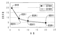
- FIG. 10 is a schematic diagram illustrating a deformed shape (estimated shape) of the sensor body calculated by the deformed shape measuring method of the first embodiment with respect to the deformed shape (actual shape) of the sensor body in the post-collision state illustrated in FIG. 9. It is sectional drawing seen from the downward direction of the bending sensor of 2nd embodiment in an attachment state. It is a schematic diagram of a collision experiment apparatus. It is a graph which shows a time-dependent change of the response of the sensor of an example.
- A is the schematic diagram which expanded the one part vicinity of the conductive filler in a sensor main body of a no-load state before bending deformation.
- B is the schematic diagram which expanded the one part vicinity of the conductive filler in a sensor main body in the state immediately after bending deformation.
- C is the schematic diagram which expanded the one part vicinity of the conductive filler in a sensor main body in the state further after immediately after bending deformation.
- FIG. 30 is a sectional view taken along line XXX-XXX in FIG. 29. It is a front view of the bending sensor of 6th embodiment. It is a graph which shows the relationship between the number of strip
- Bending sensor 10 Base material 11: Sensor body 12a to 12i: Electrodes 13a to 13i: Wiring 14: Cover film 15: Connector 16: Strain adjusting plate 17: Adhesive layer 100: Front surface 110: Coating film 120a, 120b: Curve Section 20: Mold 200: Inner peripheral surface 21: Detection section 22: Base material 23: Crack forming mold 220: Lower surface 230: Mold surface 3: Bending sensor 30 to 34: Sensor body 5: Collision experiment device 50: Striker 51: Elastic body 52: Insulating sheet 6: Bending sensor 60: Base material 61: Sensor main body 63a, 63b: Electrode 64: Cover film 7: Bending sensor 70: Base material 71: Sensor main body 72a, 72b: Electrode 73a, 73b: Wiring 74: Connector 75: Cover films 710 to 714: Detection unit 800: Sensor body 801: Matrix resin 802 Conductive filler 803: Crack 810: Sensor body 811: Base material 812a to 812
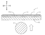
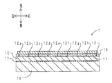
- FIG. 3 shows a front view of the bending sensor.
- FIG. 4 shows a sectional view taken along the line IV-IV in FIG.
- FIG. 5 shows an enlarged view in the circle V of FIG.
- FIG. 3 shows the cover film with the right half removed.
- the bending sensor 1 includes a base material 10, a sensor body 11, electrodes 12 a to 12 i, wires 13 a to 13 i, and a cover film 14.
- the substrate 10 is made of polyimide and has a strip shape extending in the left-right direction.
- the film thickness of the base material 10 is about 300 ⁇ m.
- a connector 15 is disposed at the right end of the substrate 10.
- the sensor body 11 has a strip shape extending in the left-right direction.
- the film thickness of the sensor body 11 is about 100 ⁇ m.
- the sensor body 11 is fixed to the surface (rear surface) of the base material 10. A strain is input in advance to the sensor body 11.
- the sensor body 11 is formed by blending carbon beads (conductive filler) with epoxy resin (matrix resin).
- the filling rate of the carbon beads is about 45 vol% when the volume of the sensor body 11 is 100 vol%.
- a large number of cracks C ⁇ b> 1 are formed in the sensor body 11 in advance.
- the crack C1 is arranged so as to extend in the direction intersecting with the arrangement direction (left-right direction) of the electrodes 12a to 12i, that is, in the thickness direction (front-rear direction) of the sensor body 11.
- About two cracks C ⁇ b> 1 are formed in the unit section U ⁇ b> 1 having a length of 2 mm that is continuous in the left-right direction of the sensor body 11.
- the electrodes 12a to 12i are arranged so that the sensor body 11 is divided into eight parts in the left-right direction. Each of the electrodes 12a to 12i has a strip shape extending in the vertical direction. All of the electrodes 12a to 12i are interposed between the sensor body 11 and the base material 10. Further, measurement sections L1 to L8 are defined by a pair of adjacent electrodes (for example, electrode 12a and electrode 12b). The electrodes 12a to 12i and the connector 15 are connected by wirings 13a to 13i, respectively.
- the cover film 14 is made of acrylic rubber and has a strip shape extending in the left-right direction.
- the cover film 14 covers the base material 10, the sensor body 11, and the wirings 13a to 13i from the rear.
- the manufacturing method of the bending sensor 1 of this embodiment has a coating material preparation process, a printing process, a bending hardening process, an unloading process, and a cover film printing process.
- sensor paint, electrode paint, wiring paint, connector paint, and cover film paint are prepared. That is, the sensor paint was prepared by using 100 parts by mass of an epoxy resin pre-curing resin (“Pernox (registered trademark) ME-562” manufactured by Nippon Pernox Co., Ltd .; liquid) and a curing agent (“Percure (registered trademark) HV- manufactured by the same company). 562 "; liquid” 150 mass parts and 300 mass parts of carbon beads (“Nika beads (registered trademark) ICB0520” manufactured by Nippon Carbon Co., Ltd., average particle diameter of about 5 m)) are mixed by blade stirring to prepare. “Dotite (registered trademark) FA-312” manufactured by Fujikura Kasei Co., Ltd.
- a cover film paint is prepared as follows. First, 100 parts by mass of an acrylic rubber polymer (“Nippol (registered trademark) AR51” manufactured by Nippon Zeon Co., Ltd.) and 1 mass of stearic acid (“Lunac (registered trademark) S30” manufactured by Kao Corporation) as a vulcanization aid And 2.5 parts by mass of vulcanization accelerator zinc dimethyldithiocarbamate (“Noxeller (registered trademark) PZ” manufactured by Ouchi Shinsei Chemical Co., Ltd.) and ferric dimethyldithiocarbamate (“Noxeller TTFE” manufactured by the same company) ) 0.5 part by mass is mixed with a roll kneader to prepare an elastomer composition. Next, the prepared elastomer composition is dissolved in 312 parts by mass of a printing solvent, ethylene glycol monobutyl ether
- a paint other than the cover film paint is printed on the surface of the substrate 10 using a screen printer.
- an electrode paint, a wiring paint, and a connector paint are sequentially printed on the surface of the substrate 10.
- the base material 10 after coating printing is left in a drying furnace at about 140 ° C. for about 30 minutes to cure the coating film.
- the electrodes 12a to 12i, the wirings 13a to 13i, and the connector 15 are formed.
- the sensor paint is printed on the surface of the substrate 10 on which the electrodes 12a to 12i and the like are formed.
- FIG. 6 shows a schematic diagram of the first half of the bending hardening process.
- FIG. 7 shows a schematic diagram of the latter half of the process.
- the base material 10 on which the coating film 110 of the sensor paint is formed is attached to the inner peripheral surface 200 of the C-shaped mold 20.
- the front surface 100 of the substrate 10 is brought into contact with the inner peripheral surface 200 of the mold 20.
- the mold 20 is placed in a drying furnace and held at about 140 ° C. for 1 hour to primarily cure the coating film 110.
- the coating film 110 is secondarily cured by holding at about 170 ° C. for 2 hours.
- the base material 10 is peeled from the mold 20 together with the cured coating film 110, and the base material 10 and the cured coating film 110 are changed from the curved state to the original planar state (see FIG. 6). Return to).
- strain is input to the cured coating film 110 (sensor body 11) and a crack C1 is formed. In this way, the sensor body 11 is produced.
- the cover film paint prepared in the paint preparation process is printed using a screen printer.
- a cover film paint is printed so as to cover the surface of the substrate 10, the sensor body 11, and the wirings 13a to 13i.
- the base material 10 after coating printing is left in a drying furnace at about 150 ° C. for about 30 minutes to cure the coating film. In this way, the cover film 14 is formed.
- the bending sensor 1 is manufactured by the above process.
- FIG. 8 is a cross-sectional view (corresponding to the IV-IV cross section in FIG. 3) as viewed from below the bending sensor before the collision of the colliding object.
- FIG. 9 is a cross-sectional view of the bending sensor as viewed from below after the collision of the colliding object.
- the bending sensor 1 is installed on the rear surface 90a of the bumper cover 90 of the automobile.
- the base material 10 is stuck on the rear surface 90a.
- the bumper cover 90 is deformed so as to sink backward.
- the deformation of the bumper cover 90 is transmitted to the bending sensor 1. That is, the deformation of the bumper cover 90 is transmitted to the sensor main body 11 and the cover film 14 via the base material 10.
- the sensor body 11 is curved together with the base material 10 and the cover film 14 into a C shape that opens forward.
- the deformed shape measurement method of the present embodiment includes a detection step, a partial shape calculation step, and an overall shape calculation step.
- the bending sensor 1 detects the bending deformation of the bumper cover 90 that is the measurement object for each of the measurement sections L1 to L8 divided by the electrodes 12a to 12i.
- the amount of strain ⁇ is calculated from the deformation data (electric resistance value) for each of the measurement sections L1 to L8, using the relationship between the electric radius and the radius of curvature up to 10 back surfaces). Then, the curvature and the radius of curvature of each of the measurement sections L1 to L8 are calculated from the obtained strain amount ⁇ . That is, the deformed shape of each of the measurement sections L1 to L8 is calculated.
- the deformed shape of the sensor body 11 is calculated by connecting the calculated deformed shapes of the measurement sections L1 to L8.
- FIG. 10 is a schematic diagram showing the deformed shape (estimated shape) of the sensor body calculated by the deformed shape measuring method of the present embodiment with respect to the deformed shape (actual shape) of the sensor body in the post-collision state shown in FIG. Indicates.
- the deformed shapes of the measurement sections L1 to L8 are joined so that the end points a to i of the adjacent measurement sections L1 to L8 share a tangent line. In this way, the deformation shape of the entire sensor body 11 is calculated. That is, the deformation shape after the collision of the bumper cover 90 (specifically, the portion of the bumper cover 90 where the bending sensor 1 is disposed) is calculated.
- the bending sensor 1 of the present embodiment the crack C1 is opened when the sensor body 11 is bent. Thereby, a conductive path is cut
- the conductive path is cut mainly by the opening of the crack C1
- a small distortion can be obtained as compared with the case where the conductive path is cut only depending on the elastic deformation of the matrix resin (see FIG. 17). It can be detected with high accuracy.
- the elastic deformation speed of the matrix resin is affected by the ambient temperature.
- the conductive path of the bending sensor 1 of the present embodiment is cut mainly by the opening of the crack C1. For this reason, the dependence of the response speed on the ambient temperature is small compared to the case where the conductive path is cut only depending on the elastic deformation of the matrix resin (see FIG. 17).
- the dependence of the response speed on the strain input speed is small.
- the sensor body 11 is covered with a cover film 14. Thereby, deterioration of the sensor main body 11 is suppressed. In addition, when unloaded after bending deformation, the sensor body 11 is easily restored to its original shape, assisted by the elastic restoring force of the cover film 14.
- the average particle diameter of the carbon beads (conductive filler) filled in the epoxy resin (matrix resin) is relatively large. For this reason, the crack C1 is easy to be formed along the interface of the conductive filler. In addition, since the crack C1 is likely to open due to bending deformation, the breaking strain of the sensor body 11 can be reduced.
- the conductive filler has a spherical shape. For this reason, a conductive filler can be mix
- the coating film of the sensor paint is cured in a state where the sensor body 11 is bent in a direction opposite to the bending deformation to be detected.
- distortion is input to the sensor body 11 in advance when it is attached to the bumper cover 90. Therefore, the total strain amount at the time of bending deformation of the sensor body 11 is the sum of the strain amount input in advance and the strain amount accompanying the bending deformation.
- the detection region can be shifted to a region that is greater than or equal to the fracture strain of the sensor body 11, that is, a region where the relationship between the strain amount and the electrical resistance is approximately linear (see FIG. 2). reference). Therefore, according to the bending sensor 1 of this embodiment, a sensitivity improves. Moreover, it becomes easy to calculate the strain amount from the electrical resistance.
- the deformed shape of the bumper cover 90 can be easily measured using the bending sensor 1. As described above, the bending sensor 1 is less likely to cause a response delay. Therefore, a time lag is unlikely to occur between the actual deformed shape of the bumper cover 90 and the calculated deformed shape. Moreover, the deformation shape of the bumper cover 90 can be accurately measured by using a region in which the relationship between the strain amount and the electrical resistance is substantially linear as the detection region of the bending sensor 1.
- ⁇ Second embodiment> The difference between the bending sensor and the deformation measuring method of the present embodiment and the bending sensor and the deformation measuring method of the first embodiment are the number of sensor main bodies and how to attach the bending sensor to the measurement object. Therefore, only the differences will be described here.
- FIG. 11 shows a cross-sectional view as seen from below the bending sensor in the mounted state.
- the measuring object 91 is made of clay and has a semi-cylindrical shape.
- the bending sensor 3 is attached to the outer peripheral curved surface 910 of the measurement object 91.
- the longitudinal direction of the bending sensor 3 and the circumferential direction of the outer peripheral curved surface 910 substantially coincide with each other.
- the bending sensor 3 includes a base material 10, five sensor bodies 30 to 34, and a cover film 14.
- the bending sensor 3 is attached so that the base material 10 contacts the outer peripheral curved surface 910.
- the base material 10 is attached to the outer peripheral curved surface 910.
- the five sensor bodies 30 to 34 are arranged in series in the longitudinal direction of the bending sensor 3.
- the configurations of the sensor bodies 30 to 34 are all the same as the configuration of the sensor body of the first embodiment.
- Each of the sensor bodies 30 to 34 is a state in which the curved state (see FIG. 7) when the sensor paint is cured is returned to the original flat state (see FIG. 6), and further curved to the opposite side. It is arranged. That is, distortion is input to the sensor bodies 30 to 34 in advance. In addition, when the bending sensor 3 is attached, cracks formed in the sensor bodies 30 to 34 are open. For this reason, many of the conductive paths are in a disconnected state.
- the sensor bodies 30 to 34 when the measurement object 91 is deformed so as to be expanded in the left-right direction and compressed in the front-rear direction, the sensor bodies 30 to 34 have a large radius of curvature as well as the outer peripheral curved surface 910 as shown by the broken line in FIG. Bend and deform in the direction That is, it bends and deforms so that it is close to a flat state. Then, the crack is closed, and the contact state between the conductive fillers is changed to restore the conductive path. As a result, the electrical resistance detected in each of the sensor main bodies 30 to 34 becomes smaller than the attachment state before bending deformation. Therefore, the bending deformation of the measuring object 91 can be detected from the output electric resistance value.
- the strain amount is calculated from the deformation data (electrical resistance value) for each measurement section in the sensor main body 30 to 34 using the relationship between the strain amount and the electric resistance of the sensor main body 30 to 34 obtained in advance. . From the obtained distortion amount, the curvature and the radius of curvature of each measurement section are calculated. Then, the deformation shape of each measurement section is calculated.
- the deformation shapes of the sensor bodies 30 to 34 in the measurement object 91 are calculated by connecting the calculated deformation shapes of the measurement sections. By connecting these deformed shapes, the deformed shape of the entire bending sensor 3, that is, the measurement object 91 is calculated.
- the bending sensor 3 of the present embodiment has the same function and effect as the bending sensor of the first embodiment. Further, the bending sensor 3 of this embodiment has five sensor bodies 30 to 34 arranged in series. For this reason, it is suitable for detecting the bending deformation of the elongated measuring object 91.
- ⁇ Third embodiment> The difference between the bending sensor and the deformation measuring method of the present embodiment and the bending sensor and the deformation measuring method of the first embodiment are the electrode shape, the configuration of the wiring, and the forming method. Therefore, only the differences will be described here.
- FIG. 21 shows an enlarged view of the vicinity of the left end of the bending sensor of the present embodiment.
- the cover film is omitted in FIG. FIG. 21 corresponds to FIG. Therefore, members corresponding to those in FIG.
- the surface shapes of the electrodes 12a and 12b are elliptical.
- the end lines of the electrodes 12a, 12b in the left-right direction (the extending direction of the sensor body 11) have curved portions 120a, 120b.
- the electrodes 12 a and 12 b are interposed between the sensor body 11 and the base material 10.
- the electrodes 12a and 12b are formed by screen-printing an electrode paint in which silver powder is blended in a resin on the substrate 10.
- the electrode paint is included in the conductive paint in the present invention.
- the wirings 13a and 13b connect the electrodes 12a and 12b and a connector (not shown), respectively.
- the wirings 13a and 13b are formed by etching a copper foil previously attached to the surface (rear surface) of the base material 10 into a predetermined pattern.
- the other electrodes 12c to 12i in the bending sensor of this embodiment are also formed in the same manner as the electrodes 12a and 12b.
- the wirings 13c to 13i are formed in the same manner as the wirings 13a and 13b.
- the bending sensor and the deformation measuring method of the present embodiment have the same functions and effects as those of the bending sensor and the deformation measuring method of the first embodiment with respect to the parts having the same configuration. Further, according to the bending sensor 1 of the present embodiment, the wirings 13a to 13i are formed by etching a copper foil. Therefore, the wirings 13a to 13i can be formed with fine lines and a narrow pitch. Thus, even if the number of electrodes 12a to 12i is large, the bending sensor 1 can be downsized.
- the electrodes 12a to 12i are formed by printing electrode paint. Therefore, the ends of the electrodes 12a to 12i are not easily squared. In other words, chamfered portions exist on the end faces in the left-right direction of the electrodes 12a to 12i (see FIG. 19). It is difficult for stress to concentrate on the chamfered portion.
- the electrode paint uses a resin as a binder. Therefore, the adhesion between the electrodes 12a to 12i and the sensor main body 11 is good.
- the electrodes 12a to 12i have an elliptical shape. That is, the left and right end lines of the electrodes 12a and 12b have the curved portions 120a and 120b. For this reason, stress is difficult to concentrate.
- ⁇ Fourth embodiment> The difference between the bending sensor and the deformation measuring method of the present embodiment and the bending sensor and the deformation measuring method of the first embodiment is that a strain adjusting plate is disposed on the front surface of the base material via an adhesive layer. Therefore, only the differences will be described here.
- FIG. 22 shows a cross-sectional view in the left-right direction of the bending sensor of the present embodiment.
- FIG. 22 corresponds to the IV-IV sectional view of FIG. 22, members corresponding to those in FIG. 4 are denoted by the same reference numerals.
- the bending sensor 1 includes a base material 10, a sensor body 11, electrodes 12a to 12i, wiring, a cover film 14, a strain adjustment plate 16, and an adhesive layer 17. Yes.
- the substrate 10, the sensor body 11, the electrodes 12a to 12i, the wiring, and the cover film 14 are the same as in the first embodiment.
- the operating temperature of the bending sensor 1 is set to about 20 ° C.
- the base material 10 is made of polyimide.
- the glass-rubber transition region of the polyimide (base material 10) is 300 to 350 ° C. That is, the temperature is higher than 30 ° C. (bending sensor 1 operating temperature + 10 ° C.).
- the strain adjusting plate 16 is made of glass cloth base epoxy resin (FR-4), and the glass-rubber transition region of the glass cloth base epoxy resin (strain adjusting plate 16) is 100 to 150 ° C. That is, it is on the higher temperature side than 30 ° C.
- the strain adjustment plate 16 has a flat plate shape extending in the left-right direction.
- the thickness of the strain adjustment plate 16 is about 0.5 mm.
- the width (vertical length) of the strain adjustment plate 16 is substantially the same as the width of the substrate 10.
- the strain adjustment plate 16 is disposed in front of the base material 10.
- the strain adjustment plate 16 and the substrate 10 are bonded via an adhesive layer 17.
- the adhesive layer 17 is made of an epoxy-based inelastic adhesive.
- the glass-rubber transition region of the inelastic adhesive (adhesive layer 17) is 40 to 70 ° C. That is, it is on the higher temperature side than 30 ° C.
- the thickness of the adhesive layer 17 is about 100 ⁇ m.
- the bending sensor and the deformation measuring method of the present embodiment have the same functions and effects as those of the bending sensor and the deformation measuring method of the first embodiment with respect to the parts having the same configuration.
- the base material 10, the strain adjusting plate 16, and the adhesive layer 17 are all materials whose glass-rubber transition region is on the higher temperature side than the operating temperature of the bending sensor 1 + 10 ° C. It is composed of For this reason, in the temperature range in which the bending sensor 1 is used, the base material 10, the strain adjustment plate 16, and the adhesive layer 17 are all in a glass state. Further, there is no state change from the glass state to the rubber state in the temperature range in which the bending sensor 1 is used.
- the base material 10 etc. there is little possibility that the bending deformation is alleviated. That is, the bending deformation is accurately transmitted to the sensor body 11. As a result, the bending deformation detection accuracy is unlikely to decrease. Further, the base material 10 and the like are all made of a hard material in a glass state. For this reason, the bending deformation is promptly transmitted to the sensor body 11. Therefore, response delay is unlikely to occur.
- ⁇ Fifth embodiment> The difference between the bending sensor of the present embodiment and the bending sensor of the first embodiment is that the number of electrodes is two, that a plurality of detectors are arranged between the electrodes, and a crack forming method. It is. Therefore, only the differences will be described here.
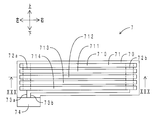
- FIG. 29 shows a front view of the bending sensor of the present embodiment.
- FIG. 30 is a sectional view taken along line XXX-XXX in FIG.
- FIG. 29 shows the cover film removed.
- the bending sensor 7 includes a base material 70, a sensor main body 71, electrodes 72 a and 72 b, wirings 73 a and 73 b, a connector 74, and a cover film 75. .
- the base material 70 is made of polyimide and has a strip shape extending in the left-right direction.
- the left-right direction corresponds to the juxtaposition direction of the present invention.
- the film thickness of the base material 70 is about 300 ⁇ m.
- a connector 74 is disposed at the lower left end of the substrate 70.
- the base material 70 is adhered to the rear surface of the bumper cover (not shown) as in the first embodiment.
- the sensor main body 71 includes five detection units 710 to 714.
- Each of the detection units 710 to 714 has a strip shape extending in the left-right direction.
- the detection units 710 to 714 are juxtaposed in the vertical direction.
- the vertical direction corresponds to the orthogonal direction of the present invention.
- the thickness of each of the detection units 710 to 714 is about 100 ⁇ m.
- the detection units 710 to 714 are fixed to the surface (rear surface) of the base material 70.
- the sensor body 71 is formed by blending carbon beads (conductive filler) with epoxy resin (matrix resin).
- the filling rate of the carbon beads is about 45 vol% when the volume of the sensor main body 71 is 100 vol%.
- a large number of cracks C1 are formed in the sensor body 71 in advance (see FIG. 5 above).
- the crack C1 is disposed so as to extend in the direction intersecting the juxtaposition direction, that is, in the thickness direction (front-rear direction) of the sensor body 71.
- About two cracks C ⁇ b> 1 are formed in the unit section U ⁇ b> 1 having a length of 2 mm that is continuous in the left-right direction of the sensor body 71.
- the electrodes 72a and 72b each have a strip shape extending in the vertical direction.
- the electrodes 72a and 72b are interposed between the base material 70 and the sensor main body 71, respectively.
- the electrode 72 a is connected to the left end of the sensor main body 71.
- the electrode 72 b is connected to the right end of the sensor main body 71.
- the five detection units 710 to 714 are installed between the pair of left and right electrodes 72a and 72b.
- the wiring 73a connects the electrode 72a and the connector 74.
- the wiring 73b connects the electrode 72b and the connector 74.
- An arithmetic device (not shown) is connected to the connector 74.
- the cover film 75 is made of acrylic rubber and has a strip shape extending in the left-right direction.
- the cover film 75 covers the base material 70, the sensor main body 71, the electrodes 72a and 72b, and the wirings 73a and 73b from the rear.
- the cover film 75 has a thickness of about 20 ⁇ m.
- the manufacturing method of the bending sensor 7 of this embodiment has a coating-material preparation process, a printing process, a hardening process, a crack formation process, and a cover film printing process.
- sensor paint, electrode paint, wiring paint, connector paint, and cover film paint are prepared. About each coating material, it is the same as said 1st embodiment. Therefore, the description is omitted here.
- a paint other than the cover film paint is printed on the surface of the substrate 70 using a screen printer.
- an electrode paint, a wiring paint, and a connector paint are sequentially printed on the surface of the base material 70.
- the base material 70 after printing the paint is allowed to stand in a drying furnace at about 140 ° C. for about 30 minutes to cure the coating film.
- the electrodes 72a and 72b, the wirings 73a and 73b, and the connector 74 are formed.
- the sensor paint is printed on the surface of the base material 70 on which the electrodes 72a, 72b and the like are formed.
- the coating film is cured by heating the substrate 70 on which the sensor paint is printed.
- the base material 70 on which the coating film of the sensor paint is formed is placed in a drying furnace and held at about 140 ° C. for 1 hour to primarily cure the coating film. Then, it hold
- the coating film is included in the “sensor body precursor” of the present invention.
- the mold surface of the crack forming mold has a curved surface.
- the base material 70 has a flat plate shape.
- the cover film paint prepared in the paint preparation process is printed using a screen printer.
- a cover film paint is printed so as to cover the surfaces of the base material 70, the sensor main body 71, the electrodes 72a and 72b, and the wirings 73a and 73b.
- the base material 70 after the paint printing is left in a drying furnace at about 150 ° C. for about 30 minutes to cure the coating film. In this way, the cover film 75 is formed.
- the bending sensor 7 is manufactured by the above process.
- the movement of the bending sensor 7 of this embodiment will be described.
- the bumper cover 90 is deformed so as to be depressed backward.
- the sensor main body 71 is curved so as to protrude rearward together with the base material 70 and the cover film 75.
- the crack C1 in the sensor main body 71 is opened.
- the conductive path is cut.
- the conductive path is cut by changing the contact state between the conductive fillers. Thereby, the detected electrical resistance becomes larger than the state before the collision. Therefore, the bending deformation of the sensor main body 71, that is, the bumper cover 90, can be detected from the output electric resistance.
- the bending sensor 7 of the present embodiment has the same function and effect as those of the bending sensor of the first embodiment with respect to the parts having the same configuration. Further, according to the bending sensor 7 of the present embodiment, the sensor main body 71 includes five detection units 710 to 714. Each of the detection units 710 to 714 extends in the left-right direction. The detection units 710 to 714 are arranged in the vertical direction. Therefore, as compared with a bending sensor having a single detection unit extending in the left-right direction, variation in electrical resistance can be reduced when the total area of the detection unit is equal.
- the detection units 710 to 714 are electrically connected to each other in parallel between the electrode 72a and the electrode 72b.
- the electrical resistances of any of the detection units 710 to 714 vary, variations in the sensor body 71 as a whole can be reduced. Therefore, variation in the combined electrical resistance R can be reduced.
- the bending sensor 7 of the present embodiment since the detection units 710 to 714 are connected in parallel, the combined electrical resistance R is unlikely to increase even if the number of the detection units 710 to 714 is increased.
- the sensor main body 71 includes five detection units 710 to 714.
- Each of the five detection units 710 to 714 extends in the left-right direction.
- the five detection units 710 to 714 are arranged in the vertical direction. Therefore, when compared with a bending sensor having a single detection unit extending in the left-right direction, the vertical width of the detection units 710 to 714 can be reduced when the total area of the detection units is the same. Therefore, the density of the crack C1 can be increased. That is, variation in electrical resistance can be reduced. Moreover, the sensitivity of the bending sensor 7 can be improved.
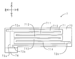
- FIG. 31 shows a front view of the bending sensor of the present embodiment.
- the cover film is removed and shown.
- the electrode 72 a is disposed at the upper left corner of the base material 70.
- the electrode 72 b is disposed at the lower right corner of the base material 70.
- the sensor body 71 connects the electrodes 72a and 72b in a zigzag manner.
- the sensor body 71 includes five detection units 710 to 714. Each of the detection units 710 to 714 has a strip shape extending in the left-right direction. The detection units 710 to 714 are juxtaposed in the vertical direction.
- the right end of the detection unit 710 and the right end of the detection unit 711, the left end of the detection unit 711 and the left end of the detection unit 712, the right end of the detection unit 712 and the right end of the detection unit 713, the left end of the detection unit 713 and the left end of the detection unit 714 are respectively It is connected. That is, the detection units 710 to 714 are connected in series.
- the bending sensor 7 of the present embodiment has the same operational effects as those of the bending sensor of the fifth embodiment with respect to the parts having the same configuration.
- the detection units 710 to 714 are electrically connected to each other in series between the electrode 72a and the electrode 72b.
- the five detection units 710 to 714 are connected in series as in one stroke. For this reason, even if the number of the detectors 710 to 714 is increased, it is not necessary to change the configuration of the connection portion between the sensor main body 71 and the electrodes 72a and 72b.
- the coating film of the sensor paint is curved in the direction opposite to the detected bending deformation. Cured.
- the degree of bending may be appropriately adjusted in consideration of the density and size of the cracks to be formed, the amount of strain input, and the like.
- a bending process may be further added after the unloading process. That is, in the bending process, the sensor body that has been returned to the flat state after curing is further repeatedly bent and returned. Alternatively, the sensor body is bent in a direction opposite to the bending direction in the bending and hardening process. By doing so, cracks can be increased and dispersed in the matrix resin.
- the method of forming a crack in the sensor body is not limited to the above embodiment.
- unevenness may be formed in advance on the surface of the substrate, and sensor paint may be printed and cured on the uneven surface. If it carries out like this, a stress will concentrate on the corner
- cracks are formed and strain is input to the sensor body.
- the predistortion does not necessarily have to be input.
- cover film synthetic rubber such as acrylic rubber or natural rubber can be used.
- resin films such as a highly insulating polyethylene and a polyethylene terephthalate (PET) other than a polyimide, can be used.
- PET polyethylene terephthalate
- the sensitivity of the bending sensor can be adjusted by adjusting the thickness of the substrate. For example, when the thickness of the base material is increased, the amount of distortion of the sensor body during bending deformation increases. Thereby, the sensitivity of a bending sensor can be improved.
- the number and arrangement of the electrodes are not limited to the above embodiment.
- the measurement section can be divided more finely.
- the shape of the measurement object can be measured by dividing it more finely.
- the deformation shape of the entire measurement object can be calculated more accurately.
- the shape of the electrode is not limited to the above embodiment. From the viewpoint of suppressing stress concentration at the end of the electrode during crack formation, it is desirable to form the electrode in a shape in which the end line in the extending direction of the sensor body has a curved portion.
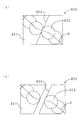
- FIG. 23 shows an example of the surface shape of the electrode. In FIG. 23, the left-right direction corresponds to the extending direction of the sensor body.
- suitable electrode surface shapes include (a) a perfect circle, (b) an ellipse, (c) an oval (a shape in which a pair of opposing semicircles are connected by a straight line), and the like. Can be mentioned.
- the electrodes are formed by printing, inkjet printing, flexographic printing, gravure printing, screen printing, pad printing, lithography, or the like can be used in addition to screen printing.
- a plurality of sensor main bodies are arranged on the surface of one base material, and all of the sensor main bodies are covered with one cover coat.
- the matrix resin and the conductive filler constituting the sensor body are not limited to the above embodiment.
- a thermosetting resin or a thermoplastic resin may be used as the matrix resin.
- the matrix resin is preferably selected in consideration of compatibility with the conductive filler described later.
- examples of the thermosetting resin include epoxy resin, alkyd resin, phenol resin, urea resin, melamine resin, unsaturated polyester resin, polyurethane, and polyimide.
- thermoplastic resin examples include polyethylene (PE), polypropylene (PP), polyvinyl chloride (PVC), polystyrene (PS), polyvinyl acetate (PVAc), polytetrafluoroethylene (PTFE), acrylonitrile-butadiene- Examples include styrene (ABS) resin, acrylic resin, polyamide (PA), polyacetal (POM), polycarbonate (PC), polyphenylene oxide (PPO), polyethylene terephthalate (PET), and polybutylene terephthalate (PBT).
- PE polyethylene
- PP polypropylene
- PVC polyvinyl chloride
- PS polystyrene
- PVAc polyvinyl acetate
- PTFE polytetrafluoroethylene
- ABS styrene
- ABS styrene
- PA polyamide
- POM polyacetal
- PC polycarbonate
- PPO polyphenylene oxide
- PET polyethylene terephthalate
- the conductive filler is not particularly limited as long as it is conductive particles. Examples thereof include fine particles such as carbon materials and metals. Of these, one can be used alone, or two or more can be used in combination.
- the aspect ratio of the conductive filler (ratio of long side to short side) is preferably in the range of 1 or more and 2 or less. When the aspect ratio is larger than 2, a one-dimensional conductive path is easily formed by contact between the conductive fillers. For this reason, it becomes difficult to obtain a desired change in electrical resistance during deformation. For example, from the viewpoint of bringing the filling state of the conductive filler in the matrix resin closer to the close-packed state, it is preferable to adopt spherical (true sphere or extremely close to true sphere) particles as the conductive filler.
- the sensor body may contain various additives in addition to the matrix resin and the conductive filler.
- the additive include an anti-aging agent, a plasticizer, a softener, and a colorant.
- the sensor body can be manufactured, for example, by applying a sensor paint containing a matrix resin, a conductive filler, etc. to the substrate surface, and then drying and curing.
- the conductive filler may be added to and mixed with the heat-melted thermoplastic resin, and then molded on the surface of the substrate.
- various known methods can be employed as a method for applying the sensor paint. For example, in addition to printing methods such as inkjet printing, flexographic printing, gravure printing, screen printing, pad printing, and lithography, dipping, spraying, bar coating, and the like can be given.
- the strain adjustment plate is disposed on the front surface of the base material via the adhesive layer.
- the material of the strain adjustment plate may be appropriately determined in consideration of the material of the base material, the use temperature of the bending sensor, and the glass-rubber transition region. Further, when the thickness of the strain adjustment plate is increased, the strain due to bending deformation can be increased. Therefore, the sensor response may be optimized by adjusting the thickness of the strain adjustment plate according to the assumed bending deformation.
- the adhesive constituting the adhesive layer may be appropriately determined in consideration of the material of the base material and the strain adjusting plate, the use temperature of the bending sensor, and the glass-rubber transition region.
- the number of sensor bodies (the number of arrangements of the detection units 710 to 714) is five.
- the number of strips is not particularly limited. It may be 10, 20 or the like. As the number of strips increases, the variation in the combined electrical resistance can be reduced. Moreover, the greater the number of strips, the greater the density of cracks. Also in this respect, the variation in the combined electric resistance can be reduced. In addition, the sensitivity of the bending sensor can be improved.
- the vertical width of the detection unit is reduced in order to increase the crack density.
- the crack density may be increased by reducing the thickness in the front-rear direction of the detection unit, that is, the sensor body.
- the density of cracks may be increased by reducing the radius of curvature of the mold surface 230 of the crack forming mold 23. In this way, a large number of cracks can be formed. For this reason, the density of cracks can be increased. Further, the density of cracks may be increased by reducing the thickness in the front-rear direction of the substrate.
- FIG. 12 shows a schematic diagram of the collision test apparatus.
- the collision experiment device 5 includes a striker 50, an elastic body 51, and an insulating sheet 52.
- the elastic body 51 is made of urethane foam and has a rectangular parallelepiped shape.
- the insulating sheet 52 is made of polyethylene and is disposed on the upper surface of the elastic body 51.
- the bending sensor 6 includes a base material 60, a sensor body 61, a pair of electrodes 63a and 63b, and a cover film 64.
- the configurations of the substrate 60, the sensor main body 61, and the cover film 64 are the same as those in the first embodiment.
- the electrode 63 a is disposed at the left end of the sensor body 61, and the electrode 63 b is disposed at the right end of the sensor body 61.
- the electrodes 63 a and 63 b are interposed between the sensor main body 61 and the base material 60.
- the bending sensor 6 is disposed on the upper surface of the insulating sheet 52 so that the base material 60 is on the upper side. A collision experiment was performed by causing a semi-cylindrical striker 50 to collide with the bending sensor 6 from above.
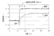
- FIG. 13 shows the change over time of the response of the sensor of the example (striker speed: 8.0 m / s).
- shaft of FIG. 13 is the resistance increase rate computed by following Formula (1).
- R 0 Initial electric resistance value before collision
- R Electric resistance value after collision
- FIG. 13 also shows the results of a conventional bending sensor (hereinafter referred to as “sensor of comparative example”).
- the sensor of the comparative example includes a sensor body in which an epoxy resin is filled with carbon beads. No cracks are formed in the sensor body.
- the electrical resistance suddenly increases immediately after the collision, and the response is completed about 6 milliseconds after the collision.
- the increase in electrical resistance is slow, and the response is not yet completed after about 6 milliseconds after the collision. Further, the rate of increase in resistance is also small compared to the sensor of the example.
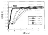
- FIG. 14 shows the change over time in the response of the sensor of the example when the striker speed was changed.
- Three types of striker speeds of 8.0 m / s, 4.0 m / s, and 2.0 m / s were used.
- speed 2.0 m / s data is indicated by a thin line.
- Four measurements were taken at each speed.
- the static response means the maximum value of electric resistance obtained when the bending sensor 6 is slowly pressed from above by the striker 50 and the deformation is maintained.
- ⁇ pre (%) Ls / Lc ⁇ 100 (2) [Ls: length in the longitudinal direction of the outermost surface of the sensor body at the time of bending hardening, Lc: length in the longitudinal direction of the center surface in the thickness direction of the substrate (constant)]
- the bending experiment was performed by attaching a plurality of test pieces (sensor body + base material) having different pre-strain amounts of the sensor body to the bending member and bending the test body in a direction opposite to the direction in which the pre-strain was input. .
- the pre-strain amount of the test piece was set to four types of 0%, 0.5%, 0.7%, and 0.9%.
- the thickness of the base material was 0.5 mm.
- the strain amount ⁇ bend input at the time of bending deformation is calculated by the following equation (3).
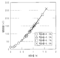
- FIG. 15 shows the change in electrical resistance with respect to the total strain measured from each test piece.
- the total strain amount is a value ( ⁇ pre + ⁇ bend ) obtained by adding the strain amount at the time of the bending experiment to the pre- strain amount.
- the total distortion amount increases as the predistortion amount increases.
- the electrical resistance has also increased. From the above, it was confirmed that a predetermined strain was input to the sensor body by heating and curing the sensor coating film in a curved state.
- the rate of increase in resistance ( ⁇ R / R 0 ; R 0 is the initial electrical resistance value before bending deformation and R is the electrical resistance value during bending deformation with respect to the curvature (1 / r) during bending deformation. ) was plotted. Then, the relationship between the curvature and the rate of increase in resistance was approximated by a linear expression to determine the contribution rate (the square of the correlation coefficient).
- FIG. 16 shows the contribution ratio to the predistortion amount.
- the contribution ratio was extremely close to 1. Specifically, the contribution rate when the predistortion amount is 0% was 0.8523, whereas the contribution rate when the predistortion amount is 0.5% is 0.9975, and the predistortion amount is When 0.7%, the contribution ratio was 0.998, and when the pre-strain amount was 0.9%, the contribution ratio was 0.99845. That is, when the pre-strain amount is 0.5%, 0.7%, and 0.9%, the relationship between the curvature and the electrical resistance can be said to be substantially linear. Thus, by inputting a predetermined strain in the sensor body in advance, the detection area of the bending sensor can be shifted to an area where the relationship between the bending deformation and the sensor response is linear.
- a bending sensor having the same configuration as that of the fourth embodiment was produced, and the strain amount with respect to bending deformation was measured by changing the thickness of the strain adjustment plate.
- the thickness of the sensor body is about 80 ⁇ m
- the thickness of the substrate is about 120 ⁇ m
- the thickness of the adhesive layer is about 100 ⁇ m.
- the thickness of the strain adjustment plate was two types of 200 ⁇ m and 900 ⁇ m.
- FIG. 24 shows the measurement results of a bending sensor (base material + sensor body) without a strain adjustment plate and an adhesive layer.
- L Longitudinal length of the outermost surface of the bending sensor at the time of bending deformation
- L 0 Longitudinal length of the outermost surface of the bending sensor in the initial state (before bending deformation)
- t Thickness of the bending sensor
- r Radius of curvature from the center of curvature to the center axis of bending
- the amount of distortion of the bending sensor having the strain adjusting plate increased compared to the bending sensor without the strain adjusting plate. Further, the thicker the strain adjustment plate, the greater the strain amount. As described above, when the strain adjustment plate is arranged, the strain due to the bending deformation can be enlarged. Further, by increasing the thickness of the strain adjustment plate, the amount of strain can be increased.
- the adhesive layer was changed to produce a bending sensor having the same configuration as that of the fourth embodiment, and the responsiveness was evaluated. Evaluation of responsiveness was performed at about 20 ° C.
- the adhesive layer two types of adhesives having different glass-rubber transition regions were used.
- FIG. 25 shows the glass-rubber transition region of the adhesive used.
- the glass-rubber transition region of the adhesive A is 40 to 70 ° C., which is higher than 30 ° C. (use temperature + 10 ° C.).
- the glass-rubber transition region of the adhesive B is ⁇ 60 to 40 ° C. and includes the range of 20 ° C. ⁇ 10 ° C. of the use temperature.
- the glass-rubber transition region of the base material and the strain adjusting plate is on the higher temperature side than 30 ° C.
- the two bending sensors are referred to as a bending sensor A and a bending sensor B depending on the type of adhesive used.
- the bending sensors A and B are both arranged on the upper surface of the insulating sheet so that the strain adjustment plate is on the upper side.
- the striker speed was 8.0 m / s.
- FIG. 26 shows the change over time of the sensor response.
- shaft of FIG. 26 is the resistance increase rate computed by above-mentioned Formula (1).
- the samples of Examples 1 to 3 are bending sensors in which detection units are connected in parallel as in the bending sensor of the fifth embodiment (see FIG. 29).
- the samples of Examples 4 to 6 are bending sensors in which detection units are connected in series, similarly to the bending sensor of the sixth embodiment (see FIG. 31).
- the sample of Reference Example 1 is a bending sensor having a single detection unit, similar to the bending sensor used in the previous collision experiment (see FIG. 12).
- the total area of the detection portions of the samples of Examples 1 to 6 and Reference Example 1 is constant. Further, unless otherwise specified below, the arrangement, shape, and material of the constituent members of each sample are constant.
- the configuration of each sample will be described with reference to FIGS. 12 and 29 to 31.
- Example 1 The configuration of the sample of Example 1 is the same as the configuration of the bending sensor of the fifth embodiment.
- the widths of the detection units 710 to 714 in the short direction are each 1 mm.
- the total length in the longitudinal direction of the detection units 710 to 714 is 50 mm.
- Example 2 The second embodiment is different from the first embodiment in that the detection units 710 to 714 are arranged in ten lines instead of five. Further, the widths of the detection units 710 to 714 in the lateral direction are different from each other in that the width is 0.5 mm instead of 1 mm. About the point other than these, it is the same.
- Example 3 The third embodiment is different from the first embodiment in that the detection units 710 to 714 are arranged in 20 lines instead of 5 lines. Further, the widths of the detection units 710 to 714 in the lateral direction are different from each other in that the width is not 0.25 mm but 0.25 mm. About the point other than these, it is the same.
- Example 4 The configuration of the sample of Example 4 is the same as the configuration of the bending sensor of the sixth embodiment.
- the widths of the detection units 710 to 714 in the short direction are each 1 mm.
- the total length in the longitudinal direction of the detection units 710 to 714 is 50 mm.
- Example 5 The fifth embodiment is different from the fourth embodiment in that the detection units 710 to 714 are arranged in 10 lines instead of 5 lines. Further, the widths of the detection units 710 to 714 in the lateral direction are different from each other in that the width is 0.5 mm instead of 1 mm. About the point other than these, it is the same.
- Example 6 The sixth embodiment is different from the fourth embodiment in that the detection units 710 to 714 are arranged in 20 lines instead of 5 lines. Further, the widths of the detection units 710 to 714 in the lateral direction are different from each other in that the width is not 0.25 mm but 0.25 mm. About the point other than these, it is the same.
- Reference example 1 The configuration of the sample of Reference Example 1 is the same as that of the bending sensor 6 shown in FIG. That is, in Reference Example 1, a single detection unit (sensor body) 61 is arranged. The width in the short direction of the detection unit 61 is 5 mm.
- FIG. 32 is a graph showing the relationship between the number of strips and the electrical resistance ratio when the detection units are connected in parallel.
- FIG. 33 is a graph showing the relationship between the number of strips and the electrical resistance ratio when the detection units are connected in series.
- FIG. 34 is a graph showing the relationship between the number of strips and the variation coefficient when the detection units are connected in parallel and when connected in series.
- the average values, maximum values, and minimum values in Table 1, FIG. 32, and FIG. 33 are the electric resistance ratios (relative values) when the average value of the electric resistance of a single detection unit is 100%. is there.
- the bending sensor and the deformed shape measuring method of the present invention are useful as means for estimating the transition of the deformed shape at the time of collision in various collision tests in addition to vehicle collision detection.
Landscapes
- Physics & Mathematics (AREA)
- General Physics & Mathematics (AREA)
- Engineering & Computer Science (AREA)
- Aviation & Aerospace Engineering (AREA)
- Chemical & Material Sciences (AREA)
- Dispersion Chemistry (AREA)
- Microelectronics & Electronic Packaging (AREA)
- Measurement Of Length, Angles, Or The Like Using Electric Or Magnetic Means (AREA)
Abstract
Description


13a~13i:配線 14:カバーフィルム 15:コネクタ 16:歪み調整板
17:接着層
100:前面 110:塗膜 120a、120b:曲線部
20:金型 200:内周面 21:検出部 22:基材 23:クラック形成用金型
220:下面 230:型面
3:曲げセンサ 30~34:センサ本体
5:衝突実験装置 50:ストライカー 51:弾性体 52:絶縁シート
6:曲げセンサ 60:基材 61:センサ本体 63a、63b:電極
64:カバーフィルム
7:曲げセンサ 70:基材 71:センサ本体 72a、72b:電極
73a、73b:配線 74:コネクタ 75:カバーフィルム
710~714:検出部
800:センサ本体 801:マトリックス樹脂 802:導電性フィラー
803:クラック
810:センサ本体 811:基材 812a~812c:電極 813:角部
814:クラック 815:面取部
90:バンパカバー 90a:後面 91:測定対象物 910:外周曲面
C1:クラック L1~L8:測定区間 O:衝突物 P:導電パス U1:単位区間
a~i:端点
[曲げセンサの構成]
まず、本実施形態の曲げセンサの構成について説明する。図3に、曲げセンサの正面図を示す。図4に、図3のIV-IV断面図を示す。図5に、図4の円V内の拡大図を示す。説明の便宜上、図3では、カバーフィルムの右半分を除去して示す。図3、図4に示すように、曲げセンサ1は、基材10と、センサ本体11と、電極12a~12iと、配線13a~13iと、カバーフィルム14と、を備えている。
次に、本実施形態の曲げセンサ1の製造方法について説明する。本実施形態の曲げセンサ1の製造方法は、塗料準備工程と、印刷工程と、曲げ硬化工程と、除荷工程と、カバーフィルム印刷工程と、を有している。
次に、本実施形態の曲げセンサ1の動きについて説明する。図8に、衝突物の衝突前における、曲げセンサの下方から見た断面図(前出図3のIV-IV断面に相当)を示す。図9に、衝突物の衝突後における、曲げセンサの下方から見た断面図を示す。
次に、本実施形態の曲げセンサ1を用いた変形形状測定方法について説明する。本実施形態の変形形状測定方法は、検出工程と、部分形状算出工程と、全体形状算出工程と、を有している。
次に、本実施形態の曲げセンサ1および変形形状測定方法の作用効果について説明する。本実施形態の曲げセンサ1によると、センサ本体11が曲がることにより、クラックC1が開口する。これにより、導電パスが切断されて、センサ本体11の電気抵抗が、速やかに増加する。したがって、応答遅れが小さい。
本実施形態の曲げセンサおよび変形測定方法と、第一実施形態の曲げセンサおよび変形測定方法と、の相違点は、センサ本体の数、および測定対象物に対する曲げセンサの取り付け方である。したがって、ここでは相違点についてのみ説明する。
本実施形態の曲げセンサおよび変形測定方法と、第一実施形態の曲げセンサおよび変形測定方法と、の相違点は、電極形状、配線の構成および形成方法である。したがって、ここでは相違点についてのみ説明する。
本実施形態の曲げセンサおよび変形測定方法と、第一実施形態の曲げセンサおよび変形測定方法と、の相違点は、基材の前面に接着層を介して歪み調整板を配置した点である。したがって、ここでは相違点についてのみ説明する。
本実施形態の曲げセンサと、第一実施形態の曲げセンサと、の相違点は、電極の数を二つにした点、当該電極間に複数の検出部を配置した点、およびクラックの形成方法である。したがって、ここでは相違点についてのみ説明する。
本実施形態の曲げセンサと第五実施形態の曲げセンサとの相違点は、二つの電極間において、センサ本体がジグザグ状に延在している点である。ここでは、相違点についてのみ説明する。
以上、本発明の曲げセンサおよび変形測定方法の実施形態について説明した。しかしながら、本発明の曲げセンサおよび変形測定方法の実施形態は上記形態に限定されるものではない。当業者が行いうる種々の変形的形態、改良的形態で実施することも可能である。
[実験方法]
電極の配置形態以外は、上記第一実施形態と同様の曲げセンサを作製した。当該曲げセンサ(以下適宜、「実施例のセンサ」と称す)について衝突実験を行い、応答性を評価した。図12に、衝突実験装置の模式図を示す。図12に示すように、衝突実験装置5は、ストライカー50と、弾性体51と、絶縁シート52と、を備えている。弾性体51は、ウレタンフォーム製であって、直方体を呈している。絶縁シート52は、ポリエチレン製であって、弾性体51の上面に配置されている。曲げセンサ6は、基材60と、センサ本体61と、一対の電極63a、63bと、カバーフィルム64と、を備えている。基材60、センサ本体61、およびカバーフィルム64の構成は、上記第一実施形態と同じである。電極63aはセンサ本体61の左端に、電極63bはセンサ本体61の右端に、各々配置されている。電極63a、63bは、センサ本体61と基材60との間に、介装されている。曲げセンサ6は、基材60が上側になるように、絶縁シート52の上面に配置されている。曲げセンサ6に対して、半円筒状のストライカー50を上方から衝突させて、衝突実験を行った。
図13に、実施例のセンサの応答の経時変化を示す(ストライカー速度:8.0m/s)。図13の縦軸は、次式(1)により算出される抵抗増加率である。
抵抗増加率(-)=ΔR/R0=(R-R0)/R0・・・(1)
[R0:衝突前の初期電気抵抗値、R:衝突後の電気抵抗値]
なお、図13には、比較のため、従来の曲げセンサ(以下、「比較例のセンサ」と称す)の結果についても併せて示す。比較例のセンサは、エポキシ樹脂にカーボンビーズが充填されてなるセンサ本体を備えている。センサ本体には、クラックは形成されていない。
[実験方法]
上記実施例のセンサについて、予めセンサ本体に入力する歪み量(以下、「予歪み量」と称す)を変化させて、曲げ実験を行った。予歪み量は、曲げ硬化工程で使用する金型内周面の曲率を変化させて調整した。ここで、予歪み量εpreは、次式(2)により算出される。
εpre(%)=Ls/Lc×100・・・(2)
[Ls:曲げ硬化時の、センサ本体の最表面の長手方向長さ、Lc:基材の厚さ方向中心面の長手方向長さ(定数)]
曲げ実験は、センサ本体の予歪み量が異なる複数の試験片(センサ本体+基材)を、曲げ部材に貼着して、予歪み入力時に湾曲した方向とは反対方向に湾曲させて行った。試験片の予歪み量は、0%、0.5%、0.7%、0.9%の四種類とした。また、基材の厚さは0.5mmとした。曲げ変形時に入力される歪み量εbendは、次式(3)により算出される。
εbend(%)=(L-L0)/L0×100=t/r・・・(3)
[L:曲げ変形時の、センサ本体の最表面の長手方向長さ、L0:初期状態(曲げ変形前)の、センサ本体の最表面の長手方向長さ、t:試験片厚さ、r:試験片の曲率半径]
図15に、各々の試験片から測定された、総歪み量に対する電気抵抗の変化を示す。総歪み量は、予歪み量に曲げ実験時の歪み量を加えた値(εpre+εbend)である。図15に示すように、予歪み量が大きくなるに従って、総歪み量が大きくなる。これに伴い、電気抵抗も大きくなっている。以上より、センサ塗料の塗膜を湾曲させた状態で、加熱硬化させることより、センサ本体に所定の歪みが入力されることが確認された。
カバーフィルムが無い以外は、上記第四実施形態と同じ構成の曲げセンサを作製し、歪み調整板の厚さを変えて、曲げ変形に対する歪み量を測定した。曲げセンサにおけるセンサ本体の厚さは約80μm、基材の厚さは約120μm、接着層の厚さは約100μmである。歪み調整板の厚さは、200μm、900μmの二種類とした。図24に、曲げ変形に対する歪み量の測定結果を示す。図24には、比較のため、歪み調整板および接着層が無い曲げセンサ(基材+センサ本体)の測定結果についても併せて示す。なお、本測定においては、曲げセンサの1/2厚さの部分を曲げの中立面とした。したがって、図24の縦軸の歪み量は、次式(4)により算出される。
歪み量=(L-L0)/L0={(r+t/2)θ-rθ}/rθ=t/2r・・・(4)
[L:曲げ変形時の、曲げセンサ最表面の長手方向長さ、L0:初期状態(曲げ変形前)の、曲げセンサ最表面の長手方向長さ、t:曲げセンサの厚さ、r:曲率中心から曲げの中心軸までの曲率半径]
図24に示すように、歪み調整板を配置した曲げセンサについては、歪み調整板が無い曲げセンサに対して、歪み量が大きくなった。また、歪み調整板が厚いほど、歪み量がより大きくなった。このように、歪み調整板を配置すると、曲げ変形による歪みを拡大することができる。また、歪み調整板を厚くすることにより、歪み量をより大きくすることができる。
接着層を変更して、上記第四実施形態と同じ構成の曲げセンサを作製し、応答性を評価した。応答性の評価は、約20℃で行った。接着層には、ガラス-ゴム転移領域が異なる二種類の接着剤を用いた。図25に、使用した接着剤のガラス-ゴム転移領域を示す。
[サンプル]
実施例1~3のサンプルは、第五実施形態の曲げセンサ(図29参照)と同様に、検出部が並列接続された曲げセンサである。実施例4~6のサンプルは、第六実施形態の曲げセンサ(図31参照)と同様に、検出部が直列接続された曲げセンサである。参考例1のサンプルは、先の衝突実験で使用した曲げセンサと同様に、単一の検出部を有する曲げセンサである(図12参照)。実施例1~6、参考例1のサンプルの検出部の総面積は一定である。また、以下に特に断らない限り、各サンプルの構成部材の配置、形状、材質は一定である。以下、図12、図29~図31を援用しながら、各サンプルの構成を説明する。
実施例1のサンプルの構成は、第五実施形態の曲げセンサの構成と同様である。また、検出部710~714の短手方向幅は、各々、1mmである。検出部710~714の長手方向全長は、各々、50mmである。
実施例2は、実施例1に対して、検出部710~714が、五条ではなく、十条配置されている点において異なっている。また、検出部710~714の短手方向幅が、各々、1mmではなく、0.5mmである点において異なっている。これら以外の点については、同様である。
実施例3は、実施例1に対して、検出部710~714が、五条ではなく、二十条配置されている点において異なっている。また、検出部710~714の短手方向幅が、各々、1mmではなく、0.25mmである点において異なっている。これら以外の点については、同様である。
実施例4のサンプルの構成は、第六実施形態の曲げセンサの構成と同様である。また、検出部710~714の短手方向幅は、各々、1mmである。検出部710~714の長手方向全長は、各々、50mmである。
実施例5は、実施例4に対して、検出部710~714が、五条ではなく、十条配置されている点において異なっている。また、検出部710~714の短手方向幅が、各々、1mmではなく、0.5mmである点において異なっている。これら以外の点については、同様である。
実施例6は、実施例4に対して、検出部710~714が、五条ではなく、二十条配置されている点において異なっている。また、検出部710~714の短手方向幅が、各々、1mmではなく、0.25mmである点において異なっている。これら以外の点については、同様である。
参考例1のサンプルの構成は、図12に示す曲げセンサ6の構成と同様である。すなわち、参考例1には、単一の検出部(センサ本体)61が配置されている。検出部61の短手方向幅は、5mmである。
各サンプルに対して、電気抵抗測定シミュレーションをモンテカルロ法により行った。単一の検出部710~714、61の電気抵抗のばらつき(平均値を100%とした場合の±方向のばらつき)が±33.3%の範囲に一様分布すると仮定し、当該ばらつきを含んだ各サンプルの合成抵抗値の平均値、標準偏差、最大値、最小値を2000回の試行により求めた。
表1にシミュレーション結果を示す。

Claims (15)
- 基材と、
該基材表面に配置され、マトリックス樹脂と、該マトリックス樹脂中に30vol%以上の充填率で充填されている導電性フィラーと、を有し、該導電性フィラー同士の接触により三次元的な導電パスが形成され、変形量が増加するに従って電気抵抗が増加するセンサ本体と、
該センサ本体を被覆するように配置され、弾性変形可能なカバーフィルムと、
該センサ本体に接続され、電気抵抗を出力可能な複数の電極と、を備える曲げセンサであって、
前記センサ本体には、曲げ変形した時に前記導電パスを切断する方向に、予めクラックが形成されていることを特徴とする曲げセンサ。 - 前記導電性フィラーの平均粒子径は、0.05μm以上100μm以下である請求項1に記載の曲げセンサ。
- 前記導電性フィラーは、球状カーボンである請求項1に記載の曲げセンサ。
- 前記センサ本体において、複数の前記電極の配置方向に連なる長さ2mm以下の単位区間を複数区画した場合に、
前記クラックは、該単位区間内に、少なくとも一つ形成されている請求項1に記載の曲げセンサ。 - 前記センサ本体には、予め歪みが入力されている請求項1に記載の曲げセンサ。
- 複数の前記電極は、導電塗料を前記基材に印刷して形成されている請求項1に記載の曲げセンサ。
- 前記電極の表面形状における、前記センサ本体の延在方向の端線は、曲線部を有する請求項6に記載の曲げセンサ。
- 複数の前記電極と各々接続されている配線を備え、
該配線は、金属箔をエッチングして形成されている請求項1に記載の曲げセンサ。 - さらに、前記基材裏面に配置される歪み調整板と、
該歪み調整板と該基材とを接着する接着層と、を備え、
該基材、該歪み調整板、および該接着層は、いずれも、貯蔵弾性率が遷移するガラス-ゴム転移領域が、曲げセンサを使用する温度範囲の下限温度-10℃よりも低温側、または上限温度+10℃よりも高温側にある材料からなる請求項1に記載の曲げセンサ。 - 二つの前記電極が並ぶ方向を並置方向、該並置方向に直交する方向を直交方向として、前記センサ本体は、二つの該電極間に、該並置方向に延在し該直交方向に並ぶ複数の検出部を有する請求項1に記載の曲げセンサ。
- 複数の前記検出部は、隣り合う二つの前記電極間において、互いに電気的に並列に接続される請求項10に記載の曲げセンサ。
- 複数の前記検出部は、隣り合う二つの前記電極間において、互いに電気的に直列に接続される請求項10に記載の曲げセンサ。
- 前記クラックは、前記センサ本体の前駆体をクラック形成用金型の型面に沿って変形させることにより形成される請求項10に記載の曲げセンサ。
- 前記検出部は、5個以上配置されている請求項10に記載の曲げセンサ。
- 請求項1ないし請求項14のいずれかに記載の曲げセンサの曲げ変形を、前記電極で区切られた測定区間ごとに検出する検出工程と、
検出された該測定区間の変形データから、該測定区間の変形形状を算出する部分形状算出工程と、
算出された該測定区間の変形形状を繋ぎ合わせて、該曲げセンサ全体の変形形状を算出する全体形状算出工程と、
を有する変形形状測定方法。
Priority Applications (3)
| Application Number | Priority Date | Filing Date | Title |
|---|---|---|---|
| CN2010800044419A CN102272566B (zh) | 2009-11-24 | 2010-09-16 | 弯曲传感器及变形形状测量方法 |
| EP10832947.5A EP2381233B1 (en) | 2009-11-24 | 2010-09-16 | Bend sensor and method of measuring deformed shape |
| US13/141,859 US8890649B2 (en) | 2009-11-24 | 2010-09-16 | Bending sensor and deformed shape measurement method |
Applications Claiming Priority (6)
| Application Number | Priority Date | Filing Date | Title |
|---|---|---|---|
| JP2009266097 | 2009-11-24 | ||
| JP2009-266097 | 2009-11-24 | ||
| JP2010-152907 | 2010-07-05 | ||
| JP2010152907A JP5654789B2 (ja) | 2009-11-24 | 2010-07-05 | 曲げセンサおよび変形形状測定方法 |
| JP2010-168868 | 2010-07-28 | ||
| JP2010168868A JP5622471B2 (ja) | 2010-07-28 | 2010-07-28 | 抵抗増加型センサおよびその製造方法 |
Publications (1)
| Publication Number | Publication Date |
|---|---|
| WO2011065100A1 true WO2011065100A1 (ja) | 2011-06-03 |
Family
ID=44674966
Family Applications (1)
| Application Number | Title | Priority Date | Filing Date |
|---|---|---|---|
| PCT/JP2010/066075 Ceased WO2011065100A1 (ja) | 2009-11-24 | 2010-09-16 | 曲げセンサおよび変形形状測定方法 |
Country Status (4)
| Country | Link |
|---|---|
| US (1) | US8890649B2 (ja) |
| EP (1) | EP2381233B1 (ja) |
| CN (1) | CN102272566B (ja) |
| WO (1) | WO2011065100A1 (ja) |
Cited By (2)
| Publication number | Priority date | Publication date | Assignee | Title |
|---|---|---|---|---|
| CN111174685A (zh) * | 2018-11-09 | 2020-05-19 | 北京纳米能源与系统研究所 | 柔性应变传感器及其制作方法 |
| CN115127666A (zh) * | 2022-06-27 | 2022-09-30 | 吉林大学 | 一种灵敏度动态可调的仿生振动检测装置及其制备方法 |
Families Citing this family (34)
| Publication number | Priority date | Publication date | Assignee | Title |
|---|---|---|---|---|
| KR100956238B1 (ko) * | 2007-12-18 | 2010-05-04 | 삼성전기주식회사 | 굴곡성 인쇄회로기판 및 그 제조방법 |
| WO2011037078A1 (ja) | 2009-09-28 | 2011-03-31 | 東海ゴム工業株式会社 | センサアセンブリおよびセンサモジュール |
| US8596137B2 (en) | 2010-07-09 | 2013-12-03 | Alliant Techsystems Inc. | Methods, devices, and systems relating to a sensing device |
| JP5486683B2 (ja) * | 2010-11-04 | 2014-05-07 | 東海ゴム工業株式会社 | 曲げセンサ |
| EP2659253B1 (en) * | 2010-12-30 | 2018-02-14 | LM Wind Power International Technology II ApS | Method and apparatus for determining loads of a wind turbine blade |
| US20140035603A1 (en) * | 2012-08-03 | 2014-02-06 | Xerox Corporation | Printed Stretch Sensor |
| DE102011082260A1 (de) * | 2011-09-07 | 2013-05-08 | Robert Bosch Gmbh | Messfühler zur Bestimmung mindestens einer Eigenschaft eines Messgases in einem Messgasraum |
| AT513245B1 (de) * | 2012-12-11 | 2014-03-15 | Siemens Vai Metals Tech Gmbh | Planheitsmessung und Messung der Eigenspannungen für ein metallisches Flachprodukt |
| JP6083225B2 (ja) * | 2012-12-13 | 2017-02-22 | ソニー株式会社 | カード、情報処理装置および情報処理プログラム |
| JP2015061057A (ja) | 2013-09-20 | 2015-03-30 | 株式会社東芝 | 歪検知素子、圧力センサ、マイクロフォン、血圧センサ及びタッチパネル |
| DE102014222949A1 (de) | 2013-11-18 | 2015-05-21 | Ford Global Technologies, Llc | Flexibler elektroresisitiver Aufprallerkennungssensor für am vorderen 'Träger befestigten Airbag |
| US9127968B2 (en) * | 2013-11-18 | 2015-09-08 | Ford Global Technologies, Llc | Flexible optical impact detection sensor for front rail mounted airbag |
| JP6356583B2 (ja) * | 2014-11-26 | 2018-07-11 | 東洋ゴム工業株式会社 | 密閉型二次電池の監視センサ、密閉型二次電池、及び、密閉型二次電池の監視方法 |
| CN104697432B (zh) * | 2015-02-04 | 2017-03-15 | 浙江大学 | 一种能实现变形自检功能的管缆 |
| EP3098691A1 (en) * | 2015-05-29 | 2016-11-30 | Manus Machinae B.V. | Flex sensor and instrumented glove |
| CN105222702A (zh) * | 2015-11-14 | 2016-01-06 | 际华三五一五皮革皮鞋有限公司 | 三维度电阻式曲面传感器 |
| CN105783697B (zh) * | 2016-05-18 | 2018-08-14 | 郑州大学 | 具有裂纹结构的柔性应变传感器及其制备方法 |
| WO2017201721A1 (zh) * | 2016-05-26 | 2017-11-30 | 深圳纽迪瑞科技开发有限公司 | 曲率半径测量器、电子设备及曲率半径测量器的制作方法 |
| CN106525296A (zh) * | 2016-10-09 | 2017-03-22 | 深圳瑞湖科技有限公司 | 一种用于触摸检测的电子皮肤 |
| TWI627381B (zh) * | 2016-10-21 | 2018-06-21 | 台灣艾華電子工業股份有限公司 | 彎曲感測器 |
| KR102044152B1 (ko) * | 2017-02-24 | 2019-11-13 | 성균관대학교산학협력단 | 크랙 치유 고분자를 포함하는 크랙 센서 및 이를 포함하는 전자 소자 |
| US10823546B1 (en) * | 2017-04-03 | 2020-11-03 | Bend Labs, Inc. | Reinforcements for inducing anisotropic bending in compliant angular displacement sensors |
| DE102017108582A1 (de) | 2017-04-21 | 2018-10-25 | Epcos Ag | Schichtwiderstand und Dünnfilmsensor |
| CN107389284B (zh) * | 2017-06-05 | 2019-01-11 | 西安电子科技大学 | 一种基于应变的框架结构弹性变形的测量方法 |
| CN107941139A (zh) * | 2017-12-06 | 2018-04-20 | 中国建筑股份有限公司 | 脚手架钢管弯曲定量测量装置及其测量方法 |
| CN112424579B (zh) * | 2018-07-09 | 2022-02-25 | 鹰野株式会社 | 压敏传感器及其制造方法、使用压敏传感器的垫系统 |
| WO2020017068A1 (ja) * | 2018-07-20 | 2020-01-23 | 帝人株式会社 | センサ装置 |
| GB2580164A (en) * | 2018-12-21 | 2020-07-15 | Imperial College Sci Tech & Medicine | A sensor |
| CN109613337B (zh) * | 2019-01-10 | 2021-01-15 | 王久钰 | 基于测量电阻的数量测量方法 |
| CN109883314B (zh) * | 2019-03-08 | 2020-06-02 | 吉林大学 | 一种柔性薄膜传感元件灵敏度测试装置及其方法 |
| DE102019204178B4 (de) * | 2019-03-26 | 2022-08-04 | Zf Friedrichshafen Ag | Verfahren zum Herstellen einer Sensoreinrichtung und Bauteil und/oder Fahrwerksbauteil mit einer solchen Sensoreinrichtung |
| CN112781482B (zh) * | 2020-08-21 | 2022-10-14 | 哈尔滨工业大学(威海) | 可变形曲面的空间曲率的测量方法以及电感式空间曲率测量敏感元件的制作方法 |
| CN115876069B (zh) * | 2022-12-29 | 2025-09-02 | 苏州浪潮智能科技有限公司 | 一种pcb基板形变侦测装置及方法 |
| CN116294961B (zh) * | 2023-02-27 | 2025-08-05 | 五邑大学 | 一种弯曲传感器及使用方法 |
Citations (12)
| Publication number | Priority date | Publication date | Assignee | Title |
|---|---|---|---|---|
| JPH0422829A (ja) * | 1990-05-17 | 1992-01-27 | Polytec Design:Kk | 圧力感知ゴム |
| US5086785A (en) | 1989-08-10 | 1992-02-11 | Abrams/Gentille Entertainment Inc. | Angular displacement sensors |
| JPH0650830A (ja) * | 1992-08-03 | 1994-02-25 | Hiroaki Yanagida | 導電性繊維束含有プラスチック複合材による歪・応力探知方法およびそれに用いる導電性繊維束含有プラスチック複合材 |
| US5583476A (en) | 1990-07-13 | 1996-12-10 | Sensitron, Inc. | Flexible potentiometer |
| JPH10239194A (ja) * | 1997-02-28 | 1998-09-11 | Matsushita Electric Works Ltd | 半導体圧力センサ |
| JP2003510216A (ja) | 1999-09-27 | 2003-03-18 | ビステオン グローバル テクノロジーズ インコーポレイテッド | 車両の衝撃センサシステム |
| JP2003344185A (ja) * | 2002-05-30 | 2003-12-03 | Fujikura Ltd | 感圧センサ |
| JP2008069313A (ja) * | 2006-09-15 | 2008-03-27 | Tokai Rubber Ind Ltd | センサー用架橋エラストマー体およびその製法 |
| JP2008070327A (ja) | 2006-09-15 | 2008-03-27 | Tokai Rubber Ind Ltd | 変形センサ |
| JP2008197060A (ja) * | 2007-02-15 | 2008-08-28 | Tokai Rubber Ind Ltd | 変形センサシステム |
| JP2009128245A (ja) * | 2007-11-26 | 2009-06-11 | Nec Corp | 内部応力測定装置および内部応力測定方法 |
| JP2009198483A (ja) | 2008-01-24 | 2009-09-03 | Tokai Rubber Ind Ltd | センサ薄膜、その製造方法、および変形センサ |
Family Cites Families (11)
| Publication number | Priority date | Publication date | Assignee | Title |
|---|---|---|---|---|
| JPS63235260A (ja) | 1987-03-20 | 1988-09-30 | Canon Inc | シ−ト後処理装置 |
| JP2538790B2 (ja) | 1987-12-26 | 1996-10-02 | 三井石油化学工業株式会社 | 膜処理方法 |
| JPH095014A (ja) * | 1995-06-19 | 1997-01-10 | Hirano Denshi:Kk | 曲げセンサ |
| US6840538B2 (en) | 1999-09-27 | 2005-01-11 | Autoliv Asp, Inc. | Method and system of actuating a deployment of a vehicle restraint system |
| US7248142B2 (en) * | 2005-08-02 | 2007-07-24 | Sensitron, Inc. | Thin deflectable resistor |
| JP5261852B2 (ja) * | 2006-09-12 | 2013-08-14 | 独立行政法人産業技術総合研究所 | 分布量計測方法およびそのための分布量センサを用いた計測システム |
| DE602007013162D1 (de) * | 2006-10-25 | 2011-04-28 | Tokai Rubber Ind Ltd | Verformungssensor |
| JP4368392B2 (ja) * | 2007-06-13 | 2009-11-18 | 東海ゴム工業株式会社 | 変形センサシステム |
| US7472587B1 (en) * | 2007-09-18 | 2009-01-06 | Infineon Technologies Ag | Tire deformation detection |
| CN101509757A (zh) * | 2009-01-17 | 2009-08-19 | 大连理工大学 | 碳纤维导电水泥基复合材料工程应变测量系统 |
| CN101551350B (zh) * | 2009-05-18 | 2012-07-11 | 南昌航空大学 | 一种建立碳纤维增强树脂基复合材料损伤自诊断系统的方法 |
-
2010
- 2010-09-16 CN CN2010800044419A patent/CN102272566B/zh not_active Expired - Fee Related
- 2010-09-16 EP EP10832947.5A patent/EP2381233B1/en not_active Not-in-force
- 2010-09-16 US US13/141,859 patent/US8890649B2/en active Active
- 2010-09-16 WO PCT/JP2010/066075 patent/WO2011065100A1/ja not_active Ceased
Patent Citations (12)
| Publication number | Priority date | Publication date | Assignee | Title |
|---|---|---|---|---|
| US5086785A (en) | 1989-08-10 | 1992-02-11 | Abrams/Gentille Entertainment Inc. | Angular displacement sensors |
| JPH0422829A (ja) * | 1990-05-17 | 1992-01-27 | Polytec Design:Kk | 圧力感知ゴム |
| US5583476A (en) | 1990-07-13 | 1996-12-10 | Sensitron, Inc. | Flexible potentiometer |
| JPH0650830A (ja) * | 1992-08-03 | 1994-02-25 | Hiroaki Yanagida | 導電性繊維束含有プラスチック複合材による歪・応力探知方法およびそれに用いる導電性繊維束含有プラスチック複合材 |
| JPH10239194A (ja) * | 1997-02-28 | 1998-09-11 | Matsushita Electric Works Ltd | 半導体圧力センサ |
| JP2003510216A (ja) | 1999-09-27 | 2003-03-18 | ビステオン グローバル テクノロジーズ インコーポレイテッド | 車両の衝撃センサシステム |
| JP2003344185A (ja) * | 2002-05-30 | 2003-12-03 | Fujikura Ltd | 感圧センサ |
| JP2008069313A (ja) * | 2006-09-15 | 2008-03-27 | Tokai Rubber Ind Ltd | センサー用架橋エラストマー体およびその製法 |
| JP2008070327A (ja) | 2006-09-15 | 2008-03-27 | Tokai Rubber Ind Ltd | 変形センサ |
| JP2008197060A (ja) * | 2007-02-15 | 2008-08-28 | Tokai Rubber Ind Ltd | 変形センサシステム |
| JP2009128245A (ja) * | 2007-11-26 | 2009-06-11 | Nec Corp | 内部応力測定装置および内部応力測定方法 |
| JP2009198483A (ja) | 2008-01-24 | 2009-09-03 | Tokai Rubber Ind Ltd | センサ薄膜、その製造方法、および変形センサ |
Non-Patent Citations (1)
| Title |
|---|
| See also references of EP2381233A4 |
Cited By (3)
| Publication number | Priority date | Publication date | Assignee | Title |
|---|---|---|---|---|
| CN111174685A (zh) * | 2018-11-09 | 2020-05-19 | 北京纳米能源与系统研究所 | 柔性应变传感器及其制作方法 |
| CN111174685B (zh) * | 2018-11-09 | 2022-06-07 | 北京纳米能源与系统研究所 | 柔性应变传感器及其制作方法 |
| CN115127666A (zh) * | 2022-06-27 | 2022-09-30 | 吉林大学 | 一种灵敏度动态可调的仿生振动检测装置及其制备方法 |
Also Published As
| Publication number | Publication date |
|---|---|
| CN102272566B (zh) | 2013-09-25 |
| EP2381233A4 (en) | 2014-07-16 |
| US8890649B2 (en) | 2014-11-18 |
| CN102272566A (zh) | 2011-12-07 |
| EP2381233B1 (en) | 2016-11-16 |
| EP2381233A1 (en) | 2011-10-26 |
| US20110307214A1 (en) | 2011-12-15 |
Similar Documents
| Publication | Publication Date | Title |
|---|---|---|
| WO2011065100A1 (ja) | 曲げセンサおよび変形形状測定方法 | |
| JP5654789B2 (ja) | 曲げセンサおよび変形形状測定方法 | |
| JP5486683B2 (ja) | 曲げセンサ | |
| Borghetti et al. | Mechanical behavior of strain sensors based on PEDOT: PSS and silver nanoparticles inks deposited on polymer substrate by inkjet printing | |
| EP2549252B1 (en) | Capacitive sensor | |
| EP3322265B1 (en) | Producing method of wired circuit board | |
| US10746612B2 (en) | Metal-metal composite ink and methods for forming conductive patterns | |
| EP2924695A1 (en) | Flexible conductive member and transducer using same | |
| EP2924406B1 (en) | Load sensor | |
| BRPI0809370A2 (pt) | Painel de proteção com função de entrada por toque para janela de exibição de instrumento eletrônico | |
| CN103582807A (zh) | 从金属和碳基体制造应变敏感传感器和/或耐应变导管 | |
| JP2010043880A (ja) | 静電容量型センサ | |
| JP2009198483A (ja) | センサ薄膜、その製造方法、および変形センサ | |
| KR101552976B1 (ko) | 전자기파 차폐 시트 및 그 제조 방법 | |
| JP5662637B2 (ja) | 荷重センサ | |
| Mosallaei et al. | Geometry analysis in screen-printed stretchable interconnects | |
| JP5622471B2 (ja) | 抵抗増加型センサおよびその製造方法 | |
| JP5662636B2 (ja) | 荷重センサ | |
| CN117387481A (zh) | 高灵敏、超柔软的硅胶弹性体应变传感器及其制备方法 | |
| JP2013232293A (ja) | 触覚センサ | |
| Selmi et al. | Organic and metallic sensors on complex 3-D object using an original method: Water transfer printing | |
| KR102138217B1 (ko) | 유연 전기 소자 및 이를 포함하는 센서 | |
| CN119714627A (zh) | 基于泊松比异向调控的超灵敏抗疲劳柔性压力传感阵列 | |
| Chen et al. | Piezoresistive Performance of a Compliant Scalable Sensor Made of Low‐Cost Exfoliated Graphite Polymer Composites | |
| JP5577170B2 (ja) | 荷重センサ |
Legal Events
| Date | Code | Title | Description |
|---|---|---|---|
| WWE | Wipo information: entry into national phase |
Ref document number: 201080004441.9 Country of ref document: CN |
|
| REEP | Request for entry into the european phase |
Ref document number: 2010832947 Country of ref document: EP |
|
| WWE | Wipo information: entry into national phase |
Ref document number: 2010832947 Country of ref document: EP |
|
| 121 | Ep: the epo has been informed by wipo that ep was designated in this application |
Ref document number: 10832947 Country of ref document: EP Kind code of ref document: A1 |
|
| WWE | Wipo information: entry into national phase |
Ref document number: 13141859 Country of ref document: US |
|
| NENP | Non-entry into the national phase |
Ref country code: DE |