WO2011065343A1 - 光電変換装置及びその製造方法 - Google Patents
光電変換装置及びその製造方法 Download PDFInfo
- Publication number
- WO2011065343A1 WO2011065343A1 PCT/JP2010/070853 JP2010070853W WO2011065343A1 WO 2011065343 A1 WO2011065343 A1 WO 2011065343A1 JP 2010070853 W JP2010070853 W JP 2010070853W WO 2011065343 A1 WO2011065343 A1 WO 2011065343A1
- Authority
- WO
- WIPO (PCT)
- Prior art keywords
- layer
- type layer
- photoelectric conversion
- microcrystalline silicon
- type
- Prior art date
- Legal status (The legal status is an assumption and is not a legal conclusion. Google has not performed a legal analysis and makes no representation as to the accuracy of the status listed.)
- Ceased
Links
Images


Classifications
-
- H—ELECTRICITY
- H10—SEMICONDUCTOR DEVICES; ELECTRIC SOLID-STATE DEVICES NOT OTHERWISE PROVIDED FOR
- H10F—INORGANIC SEMICONDUCTOR DEVICES SENSITIVE TO INFRARED RADIATION, LIGHT, ELECTROMAGNETIC RADIATION OF SHORTER WAVELENGTH OR CORPUSCULAR RADIATION
- H10F77/00—Constructional details of devices covered by this subclass
- H10F77/10—Semiconductor bodies
- H10F77/16—Material structures, e.g. crystalline structures, film structures or crystal plane orientations
- H10F77/162—Non-monocrystalline materials, e.g. semiconductor particles embedded in insulating materials
- H10F77/164—Polycrystalline semiconductors
- H10F77/1642—Polycrystalline semiconductors including only Group IV materials
- H10F77/1645—Polycrystalline semiconductors including only Group IV materials including microcrystalline silicon
-
- C—CHEMISTRY; METALLURGY
- C23—COATING METALLIC MATERIAL; COATING MATERIAL WITH METALLIC MATERIAL; CHEMICAL SURFACE TREATMENT; DIFFUSION TREATMENT OF METALLIC MATERIAL; COATING BY VACUUM EVAPORATION, BY SPUTTERING, BY ION IMPLANTATION OR BY CHEMICAL VAPOUR DEPOSITION, IN GENERAL; INHIBITING CORROSION OF METALLIC MATERIAL OR INCRUSTATION IN GENERAL
- C23C—COATING METALLIC MATERIAL; COATING MATERIAL WITH METALLIC MATERIAL; SURFACE TREATMENT OF METALLIC MATERIAL BY DIFFUSION INTO THE SURFACE, BY CHEMICAL CONVERSION OR SUBSTITUTION; COATING BY VACUUM EVAPORATION, BY SPUTTERING, BY ION IMPLANTATION OR BY CHEMICAL VAPOUR DEPOSITION, IN GENERAL
- C23C16/00—Chemical coating by decomposition of gaseous compounds, without leaving reaction products of surface material in the coating, i.e. chemical vapour deposition [CVD] processes
- C23C16/22—Chemical coating by decomposition of gaseous compounds, without leaving reaction products of surface material in the coating, i.e. chemical vapour deposition [CVD] processes characterised by the deposition of inorganic material, other than metallic material
- C23C16/24—Deposition of silicon only
-
- C—CHEMISTRY; METALLURGY
- C23—COATING METALLIC MATERIAL; COATING MATERIAL WITH METALLIC MATERIAL; CHEMICAL SURFACE TREATMENT; DIFFUSION TREATMENT OF METALLIC MATERIAL; COATING BY VACUUM EVAPORATION, BY SPUTTERING, BY ION IMPLANTATION OR BY CHEMICAL VAPOUR DEPOSITION, IN GENERAL; INHIBITING CORROSION OF METALLIC MATERIAL OR INCRUSTATION IN GENERAL
- C23C—COATING METALLIC MATERIAL; COATING MATERIAL WITH METALLIC MATERIAL; SURFACE TREATMENT OF METALLIC MATERIAL BY DIFFUSION INTO THE SURFACE, BY CHEMICAL CONVERSION OR SUBSTITUTION; COATING BY VACUUM EVAPORATION, BY SPUTTERING, BY ION IMPLANTATION OR BY CHEMICAL VAPOUR DEPOSITION, IN GENERAL
- C23C16/00—Chemical coating by decomposition of gaseous compounds, without leaving reaction products of surface material in the coating, i.e. chemical vapour deposition [CVD] processes
- C23C16/44—Chemical coating by decomposition of gaseous compounds, without leaving reaction products of surface material in the coating, i.e. chemical vapour deposition [CVD] processes characterised by the method of coating
- C23C16/52—Controlling or regulating the coating process
-
- H—ELECTRICITY
- H10—SEMICONDUCTOR DEVICES; ELECTRIC SOLID-STATE DEVICES NOT OTHERWISE PROVIDED FOR
- H10F—INORGANIC SEMICONDUCTOR DEVICES SENSITIVE TO INFRARED RADIATION, LIGHT, ELECTROMAGNETIC RADIATION OF SHORTER WAVELENGTH OR CORPUSCULAR RADIATION
- H10F10/00—Individual photovoltaic cells, e.g. solar cells
-
- H—ELECTRICITY
- H10—SEMICONDUCTOR DEVICES; ELECTRIC SOLID-STATE DEVICES NOT OTHERWISE PROVIDED FOR
- H10F—INORGANIC SEMICONDUCTOR DEVICES SENSITIVE TO INFRARED RADIATION, LIGHT, ELECTROMAGNETIC RADIATION OF SHORTER WAVELENGTH OR CORPUSCULAR RADIATION
- H10F10/00—Individual photovoltaic cells, e.g. solar cells
- H10F10/10—Individual photovoltaic cells, e.g. solar cells having potential barriers
- H10F10/17—Photovoltaic cells having only PIN junction potential barriers
-
- H—ELECTRICITY
- H10—SEMICONDUCTOR DEVICES; ELECTRIC SOLID-STATE DEVICES NOT OTHERWISE PROVIDED FOR
- H10F—INORGANIC SEMICONDUCTOR DEVICES SENSITIVE TO INFRARED RADIATION, LIGHT, ELECTROMAGNETIC RADIATION OF SHORTER WAVELENGTH OR CORPUSCULAR RADIATION
- H10F71/00—Manufacture or treatment of devices covered by this subclass
-
- H—ELECTRICITY
- H10—SEMICONDUCTOR DEVICES; ELECTRIC SOLID-STATE DEVICES NOT OTHERWISE PROVIDED FOR
- H10F—INORGANIC SEMICONDUCTOR DEVICES SENSITIVE TO INFRARED RADIATION, LIGHT, ELECTROMAGNETIC RADIATION OF SHORTER WAVELENGTH OR CORPUSCULAR RADIATION
- H10F71/00—Manufacture or treatment of devices covered by this subclass
- H10F71/121—The active layers comprising only Group IV materials
- H10F71/1224—The active layers comprising only Group IV materials comprising microcrystalline silicon
-
- H—ELECTRICITY
- H10—SEMICONDUCTOR DEVICES; ELECTRIC SOLID-STATE DEVICES NOT OTHERWISE PROVIDED FOR
- H10F—INORGANIC SEMICONDUCTOR DEVICES SENSITIVE TO INFRARED RADIATION, LIGHT, ELECTROMAGNETIC RADIATION OF SHORTER WAVELENGTH OR CORPUSCULAR RADIATION
- H10F77/00—Constructional details of devices covered by this subclass
- H10F77/10—Semiconductor bodies
- H10F77/16—Material structures, e.g. crystalline structures, film structures or crystal plane orientations
- H10F77/162—Non-monocrystalline materials, e.g. semiconductor particles embedded in insulating materials
- H10F77/166—Amorphous semiconductors
- H10F77/1662—Amorphous semiconductors including only Group IV materials
-
- H—ELECTRICITY
- H10—SEMICONDUCTOR DEVICES; ELECTRIC SOLID-STATE DEVICES NOT OTHERWISE PROVIDED FOR
- H10P—GENERIC PROCESSES OR APPARATUS FOR THE MANUFACTURE OR TREATMENT OF DEVICES COVERED BY CLASS H10
- H10P14/00—Formation of materials, e.g. in the shape of layers or pillars
- H10P14/20—Formation of materials, e.g. in the shape of layers or pillars of semiconductor materials
- H10P14/24—Formation of materials, e.g. in the shape of layers or pillars of semiconductor materials using chemical vapour deposition [CVD]
-
- H—ELECTRICITY
- H10—SEMICONDUCTOR DEVICES; ELECTRIC SOLID-STATE DEVICES NOT OTHERWISE PROVIDED FOR
- H10P—GENERIC PROCESSES OR APPARATUS FOR THE MANUFACTURE OR TREATMENT OF DEVICES COVERED BY CLASS H10
- H10P14/00—Formation of materials, e.g. in the shape of layers or pillars
- H10P14/20—Formation of materials, e.g. in the shape of layers or pillars of semiconductor materials
- H10P14/34—Deposited materials, e.g. layers
- H10P14/3402—Deposited materials, e.g. layers characterised by the chemical composition
- H10P14/3404—Deposited materials, e.g. layers characterised by the chemical composition being Group IVA materials
- H10P14/3411—Silicon, silicon germanium or germanium
-
- H—ELECTRICITY
- H10—SEMICONDUCTOR DEVICES; ELECTRIC SOLID-STATE DEVICES NOT OTHERWISE PROVIDED FOR
- H10P—GENERIC PROCESSES OR APPARATUS FOR THE MANUFACTURE OR TREATMENT OF DEVICES COVERED BY CLASS H10
- H10P14/00—Formation of materials, e.g. in the shape of layers or pillars
- H10P14/20—Formation of materials, e.g. in the shape of layers or pillars of semiconductor materials
- H10P14/34—Deposited materials, e.g. layers
- H10P14/3438—Doping during depositing
- H10P14/3441—Conductivity type
-
- H—ELECTRICITY
- H10—SEMICONDUCTOR DEVICES; ELECTRIC SOLID-STATE DEVICES NOT OTHERWISE PROVIDED FOR
- H10P—GENERIC PROCESSES OR APPARATUS FOR THE MANUFACTURE OR TREATMENT OF DEVICES COVERED BY CLASS H10
- H10P14/00—Formation of materials, e.g. in the shape of layers or pillars
- H10P14/20—Formation of materials, e.g. in the shape of layers or pillars of semiconductor materials
- H10P14/34—Deposited materials, e.g. layers
- H10P14/3451—Structure
- H10P14/3452—Microstructure
- H10P14/3456—Polycrystalline
-
- H—ELECTRICITY
- H10—SEMICONDUCTOR DEVICES; ELECTRIC SOLID-STATE DEVICES NOT OTHERWISE PROVIDED FOR
- H10P—GENERIC PROCESSES OR APPARATUS FOR THE MANUFACTURE OR TREATMENT OF DEVICES COVERED BY CLASS H10
- H10P14/00—Formation of materials, e.g. in the shape of layers or pillars
- H10P14/20—Formation of materials, e.g. in the shape of layers or pillars of semiconductor materials
- H10P14/29—Formation of materials, e.g. in the shape of layers or pillars of semiconductor materials characterised by the substrates
- H10P14/2901—Materials
- H10P14/2922—Materials being non-crystalline insulating materials, e.g. glass or polymers
-
- H—ELECTRICITY
- H10—SEMICONDUCTOR DEVICES; ELECTRIC SOLID-STATE DEVICES NOT OTHERWISE PROVIDED FOR
- H10P—GENERIC PROCESSES OR APPARATUS FOR THE MANUFACTURE OR TREATMENT OF DEVICES COVERED BY CLASS H10
- H10P14/00—Formation of materials, e.g. in the shape of layers or pillars
- H10P14/20—Formation of materials, e.g. in the shape of layers or pillars of semiconductor materials
- H10P14/29—Formation of materials, e.g. in the shape of layers or pillars of semiconductor materials characterised by the substrates
- H10P14/2924—Structures
- H10P14/2925—Surface structures
-
- H—ELECTRICITY
- H10—SEMICONDUCTOR DEVICES; ELECTRIC SOLID-STATE DEVICES NOT OTHERWISE PROVIDED FOR
- H10P—GENERIC PROCESSES OR APPARATUS FOR THE MANUFACTURE OR TREATMENT OF DEVICES COVERED BY CLASS H10
- H10P14/00—Formation of materials, e.g. in the shape of layers or pillars
- H10P14/20—Formation of materials, e.g. in the shape of layers or pillars of semiconductor materials
- H10P14/32—Formation of materials, e.g. in the shape of layers or pillars of semiconductor materials characterised by intermediate layers between substrates and deposited layers
- H10P14/3202—Materials thereof
- H10P14/3241—Materials thereof being conductive materials
-
- Y—GENERAL TAGGING OF NEW TECHNOLOGICAL DEVELOPMENTS; GENERAL TAGGING OF CROSS-SECTIONAL TECHNOLOGIES SPANNING OVER SEVERAL SECTIONS OF THE IPC; TECHNICAL SUBJECTS COVERED BY FORMER USPC CROSS-REFERENCE ART COLLECTIONS [XRACs] AND DIGESTS
- Y02—TECHNOLOGIES OR APPLICATIONS FOR MITIGATION OR ADAPTATION AGAINST CLIMATE CHANGE
- Y02E—REDUCTION OF GREENHOUSE GAS [GHG] EMISSIONS, RELATED TO ENERGY GENERATION, TRANSMISSION OR DISTRIBUTION
- Y02E10/00—Energy generation through renewable energy sources
- Y02E10/50—Photovoltaic [PV] energy
- Y02E10/545—Microcrystalline silicon PV cells
-
- Y—GENERAL TAGGING OF NEW TECHNOLOGICAL DEVELOPMENTS; GENERAL TAGGING OF CROSS-SECTIONAL TECHNOLOGIES SPANNING OVER SEVERAL SECTIONS OF THE IPC; TECHNICAL SUBJECTS COVERED BY FORMER USPC CROSS-REFERENCE ART COLLECTIONS [XRACs] AND DIGESTS
- Y02—TECHNOLOGIES OR APPLICATIONS FOR MITIGATION OR ADAPTATION AGAINST CLIMATE CHANGE
- Y02E—REDUCTION OF GREENHOUSE GAS [GHG] EMISSIONS, RELATED TO ENERGY GENERATION, TRANSMISSION OR DISTRIBUTION
- Y02E10/00—Energy generation through renewable energy sources
- Y02E10/50—Photovoltaic [PV] energy
- Y02E10/548—Amorphous silicon PV cells
-
- Y—GENERAL TAGGING OF NEW TECHNOLOGICAL DEVELOPMENTS; GENERAL TAGGING OF CROSS-SECTIONAL TECHNOLOGIES SPANNING OVER SEVERAL SECTIONS OF THE IPC; TECHNICAL SUBJECTS COVERED BY FORMER USPC CROSS-REFERENCE ART COLLECTIONS [XRACs] AND DIGESTS
- Y02—TECHNOLOGIES OR APPLICATIONS FOR MITIGATION OR ADAPTATION AGAINST CLIMATE CHANGE
- Y02P—CLIMATE CHANGE MITIGATION TECHNOLOGIES IN THE PRODUCTION OR PROCESSING OF GOODS
- Y02P70/00—Climate change mitigation technologies in the production process for final industrial or consumer products
- Y02P70/50—Manufacturing or production processes characterised by the final manufactured product
Definitions
- the present invention relates to a photoelectric conversion device and a manufacturing method thereof.
- Solar cells using polycrystalline, microcrystalline, or amorphous silicon as a photoelectric conversion layer are known.
- a photoelectric conversion device having a structure in which microcrystalline or amorphous silicon thin films are stacked has attracted attention from the viewpoint of resource consumption, cost reduction, and efficiency.
- a photoelectric conversion device is formed by sequentially stacking a first electrode, a photoelectric conversion cell made of a semiconductor thin film, and a second electrode on a substrate having an insulating surface.
- the photoelectric conversion cell is configured by stacking a p-type layer, an i-type layer, and an n-type layer from the light incident side.
- a method for improving the conversion efficiency of a photoelectric conversion device it is known to stack two or more types of photoelectric conversion cells in the light incident direction.
- a first photoelectric conversion unit including a photoelectric conversion layer having a wide band gap is disposed on the light incident side of the photoelectric conversion device, and then a photoelectric conversion layer having a narrower band gap than the first photoelectric conversion unit.
- a second photoelectric conversion unit including is disposed.
- photoelectric conversion can be performed over a wide wavelength range of incident light, and the conversion efficiency of the entire apparatus can be improved.
- a structure in which an amorphous silicon (a-Si) photoelectric conversion unit is a top cell and a microcrystalline silicon ( ⁇ c-Si) photoelectric conversion unit is a bottom cell is known.
- the ⁇ c-Si photoelectric conversion unit using microcrystalline silicon containing a microcrystalline phase as an i-type layer as a power generation layer has advantages such as excellent light stability compared to amorphous silicon, but dangling bonds are included in the film. There is a problem that there are many defects due to the above. Therefore, a technique for improving the conversion efficiency of photovoltaic power by changing the crystallization rate of silicon in the i-type layer and the hydrogen content in the layer thickness direction has been considered (for example, see Patent Document 1).
- the ratio (crystallization rate) between the crystalline phase and the amorphous phase in the film can be changed depending on the film forming conditions.
- the film is formed under the condition that a microcrystalline silicon thin film having a high crystallization rate is formed near the center of the panel of the photoelectric conversion device.
- the dispersion of the crystallization rate in the panel surface of the photoelectric conversion device becomes large, and a photoelectric conversion cell having a high crystallization rate and high photoelectric conversion efficiency is obtained near the center of the panel. In the vicinity, only a photoelectric conversion cell having a low crystallization rate and a low photoelectric conversion efficiency can be obtained. As a result, there may be a problem that the conversion efficiency is lowered when the entire panel of the photoelectric conversion device is viewed.
- One embodiment of the present invention is a process for forming an i-type layer in a method for manufacturing a photoelectric conversion device having a stacked structure of a p-type layer, an i-type layer including a microcrystalline silicon layer serving as a power generation layer, and an n-type layer.
- a method for manufacturing a photoelectric conversion device including a step of forming a second microcrystalline silicon layer.
- Another embodiment of the present invention is a photoelectric conversion device including a stacked structure of a p-type layer, an i-type layer including a microcrystalline silicon layer serving as a power generation layer, and an n-type layer, wherein the i-type layer includes the first microcrystal.
- Photoelectric conversion having a stacked structure of a silicon layer and a second microcrystalline silicon layer formed under conditions where the crystallization rate is higher than that of the first microcrystalline silicon layer and the in-plane distribution of the crystallization rate is low Device.
- dispersion of photoelectric conversion efficiency within the panel surface in the photoelectric conversion device can be reduced.
- FIG. 6 is a diagram showing a distribution of crystallization ratios of i-type layers of ⁇ c-Si units in the embodiment of the present invention. It is a figure which shows the characteristic measurement point of the photoelectric conversion apparatus in the Example and comparative example of this invention. It is a figure which shows the measurement result of the crystallization rate of the i-type layer of the ⁇ c-Si unit in the embodiment of the present invention.
- FIG. 1 is a cross-sectional view showing the structure of a photoelectric conversion device 100 according to an embodiment of the present invention.
- the transparent insulating substrate 10 is a light incident side, the transparent conductive film 12 from the light incident side, and amorphous silicon (a-Si) having a wide band gap as a top cell (photoelectric conversion) Unit 102, intermediate layer 14, microcrystalline silicon ( ⁇ c-Si) (photoelectric conversion) unit 104 having a narrower band gap than a-Si unit 102 as a bottom cell, first back electrode layer 16, second back electrode layer 18, filler 20 and a protective film 22 are stacked.
- a-Si unit 102 and the ⁇ c-Si unit 104 functions as a power generation layer of the photoelectric conversion device 100 in the embodiment of the present invention.
- the photoelectric conversion device 100 according to the embodiment of the present invention is characterized by the i-type layer included in the ⁇ c-Si unit 104, the i-type layer included in the ⁇ c-Si unit 104 will be particularly described in detail. .
- the transparent insulating substrate 10 for example, a material having transparency in at least a visible light wavelength region such as a glass substrate or a plastic substrate can be applied.
- a transparent conductive film 12 is formed on the transparent insulating substrate 10.
- the transparent conductive film 12 is doped with tin oxide (SnO 2 ), zinc oxide (ZnO), indium tin oxide (ITO), etc. with tin (Sn), antimony (Sb), fluorine (F), aluminum (Al), etc. It is preferable to use at least one or a combination of a plurality of transparent conductive oxides (TCO).
- zinc oxide (ZnO) is preferable because it has high translucency, low resistivity, and excellent plasma resistance.
- the transparent conductive film 12 can be formed by, for example, sputtering.
- the film thickness of the transparent conductive film 12 is preferably in the range of 0.5 ⁇ m to 5 ⁇ m. Moreover, it is preferable to provide unevenness having a light confinement effect on the surface of the transparent conductive film 12.
- an a-Si unit 102 is formed by sequentially laminating a p-type layer, an i-type layer, and an n-type silicon thin film.
- the a-Si unit 102 includes silicon-containing gas such as silane (SiH 4 ), disilane (Si 2 H 6 ), dichlorosilane (SiH 2 Cl 2 ), carbon-containing gas such as methane (CH 4 ), diborane (B 2 H 6 ) formed by plasma CVD in which a mixed gas obtained by mixing a p-type dopant-containing gas such as phosphine (PH 3 ) and a dilute gas such as phosphine (PH 3 ) and a diluent gas such as hydrogen (H 2 ) is formed into a plasma.
- silicon-containing gas such as silane (SiH 4 ), disilane (Si 2 H 6 ), dichlorosilane (SiH 2 Cl 2 ), carbon-containing gas such as methane (CH
- the RF plasma CVD for example, 13.56 MHz RF plasma CVD is preferably applied.
- the RF plasma CVD can be a parallel plate type. It is good also as a structure which provided the gas shower hole for supplying the mixed gas of a raw material in the side which does not arrange
- the input power density of plasma is preferably 5 mW / cm 2 or more and 100 mW / cm 2 or less.
- the p-type layer, i-type layer, and n-type layer are formed in separate film formation chambers.
- the film forming chamber can be evacuated by a vacuum pump and has an electrode for RF plasma CVD.
- a transfer device for the transparent insulating substrate 10, a power source and matching device for RF plasma CVD, piping for gas supply, and the like are attached.
- the p-type layer is formed on the transparent conductive film 12.
- the p-type layer is a p-type amorphous silicon layer (p-type a-Si: H) having a thickness of 10 nm to 100 nm doped with a p-type dopant (boron or the like).
- the film quality of the p-type layer can be changed by adjusting the mixing ratio of the silicon-containing gas, the carbon-containing gas, the p-type dopant-containing gas and the dilution gas, the pressure, and the high frequency power for plasma generation.
- the i-type layer is an undoped amorphous silicon film of 50 nm to 500 nm formed on the p-type layer.
- the film quality of the i-type layer can be changed by adjusting the mixing ratio of the silicon-containing gas and the dilution gas, the pressure, and the high frequency power for plasma generation.
- the i-type layer serves as a power generation layer of the a-Si unit 102.
- the n-type layer is an n-type amorphous silicon layer (n-type a-Si: H) having a thickness of 10 nm to 100 nm doped with an n-type dopant (such as phosphorus) formed on the i-type layer or n-type microcrystalline silicon.
- Layer (n-type ⁇ c-Si: H) having a thickness of 10 nm to 100 nm doped with an n-type dopant (such as phosphorus) formed on the i-type layer or n-type microcrystalline silicon.
- the film quality of the n-type layer can be changed by adjusting the mixing ratio of the silicon-containing gas, the carbon-containing gas, the n-type dopant-containing gas and the dilution gas, the pressure, and the high-frequency power for plasma generation.
- the intermediate layer 14 is formed on the a-Si unit 102.
- the intermediate layer 14 is preferably made of a transparent conductive oxide (TCO) such as zinc oxide (ZnO) or silicon oxide (SiOx).
- TCO transparent conductive oxide
- ZnO zinc oxide
- SiOx silicon oxide
- Mg magnesium
- the intermediate layer 14 can be formed by, for example, sputtering.
- the film thickness of the intermediate layer 14 is preferably in the range of 10 nm to 200 nm. The intermediate layer 14 need not be provided.
- the ⁇ c-Si unit 104 includes silicon-containing gases such as silane (SiH 4 ), disilane (Si 2 H 6 ), dichlorosilane (SiH 2 Cl 2 ), carbon-containing gases such as methane (CH 4 ), diborane (B 2 H 6 ) formed by plasma CVD in which a mixed gas obtained by mixing a p-type dopant-containing gas such as phosphine (PH 3 ) and a dilute gas such as phosphine (PH 3 ) and a diluent gas such as hydrogen (H 2 ) is formed into a plasma.
- silicon-containing gases such as silane (SiH 4 ), disilane (Si 2 H 6 ), dichlorosilane (SiH 2 Cl 2 ), carbon-containing gases such as methane (CH 4 ), diborane (B 2 H 6 ) formed by plasma CVD in which a mixed gas obtained by mixing a p-type dopant-containing gas such as
- RF plasma CVD for example, RF plasma CVD or VHF plasma CVD is preferably applied.
- RF plasma CVD and VHF plasma CVD can be parallel plate types. It is good also as a structure which provided the gas shower hole for supplying the mixed gas of a raw material in the side which does not arrange
- Input power density of the plasma is preferably set to 5 mW / cm 2 or more 1000 mW / cm 2 or less.
- the p-type layer 40 is formed on the intermediate layer 14 or the n-type layer of the a-Si unit 102.
- the p-type layer 40 is a p-type microcrystalline silicon layer (p-type ⁇ c-Si: H) having a thickness of 5 nm to 50 nm doped with a p-type dopant (boron or the like).
- the film quality of the p-type layer 40 can be changed by adjusting the mixing ratio of the silicon-containing gas, the carbon-containing gas, the p-type dopant-containing gas and the dilution gas, the pressure, and the high frequency power for plasma generation.
- the i-type layer 42 is an undoped microcrystalline silicon film formed on the p-type layer 40 and having a thickness of 0.5 ⁇ m to 5 ⁇ m. Details of the i-type layer 42 will be described later.
- the n-type layer 44 is formed on the i-type layer 42.
- the n-type layer 44 is an n-type microcrystalline silicon layer (n-type ⁇ c-Si: H) doped with an n-type dopant (such as phosphorus) and having a thickness of 5 nm to 50 nm.
- the ⁇ c-Si unit 104 is not limited to this, and any unit that uses an i-type microcrystalline silicon layer (i-type ⁇ c-Si: H) described below as a power generation layer may be used.
- the i-type layer 42 is formed under at least two different film forming conditions.
- the crystallization rate Xc is low near the center in the plane of the substrate when it is formed as a single film on a glass substrate or the like, and as shown by the solid line in FIG.
- the first i-type layer 42a is formed under film forming conditions that increase the uniformity of the crystallization rate Xc.
- the crystallization rate Xc of the first i-type layer 42a is preferably about 2 to 4 when about 500 nm is formed as a single film.
- the crystallization rate is higher than that of the first i-type layer 42a near the center in the plane of the substrate when a single film is formed on the glass substrate.
- the second i-type layer 42b is formed under film-forming conditions in which the uniformity of the crystallization rate Xc is lower than that of the first i-type layer 42a in the plane of the substrate, as indicated by a broken line in FIG. To do.
- the crystallization rate Xc of the second i-type layer 42b is preferably about 4 to 6 when about 500 nm is formed as a single film.
- the first i-type layer 42a is formed by a plasma film forming method while introducing a mixed gas having a silane (SiH 4 ) / hydrogen (H 2 ) ratio of 0.005 to 0.1 at a pressure of 1330 Pa to 4000 Pa. It is preferable to form a film.
- a plasma film forming method it is preferable to apply a VHF plasma film forming method with a frequency of 13.56 MHz to 70 MHz.
- the substrate temperature during film formation be 160 ° C. or higher and 230 ° C. or lower, and the power introduced into the plasma be 0.05 W / cm 2 or higher and 5 W / cm 2 or lower.
- the second i-type layer 42b is formed by a plasma film forming method while introducing a mixed gas having a silane (SiH 4 ) / hydrogen (H 2 ) ratio of 0.005 to 0.1 at a pressure of 1330 Pa to 4000 Pa. It is preferable to form a film.
- a plasma film forming method it is preferable to apply a VHF plasma film forming method with a frequency of 13.56 MHz to 70 MHz.
- the substrate temperature during film formation be 160 ° C. or higher and 230 ° C. or lower, and the power introduced into the plasma be 0.05 W / cm 2 or higher and 5 W / cm 2 or lower.
- the film thickness of the first i-type layer 42a is preferably 100 nm to 2000 nm, and more preferably 500 nm to 1500 nm.
- the film thickness of the second i-type layer 42b is preferably 500 nm or more and 3000 nm or less, and more preferably 1000 nm or more and 2500 nm or less. If the film thickness of the first i-type layer 42a is less than 100 nm, it is difficult to obtain the effect of reducing the dispersion of photoelectric conversion efficiency within the panel surface.
- the film thickness of the first i-type layer 42a is greater than 2500 nm or the film thickness of the second i-type layer 42b is greater than 3500 nm, the total of the first i-type layer 42a and the second i-type layer 42b The film thickness becomes too thick, and the photoelectric conversion efficiency may be reduced.
- a laminated structure of a reflective metal and a transparent conductive oxide (TCO) is formed on the ⁇ c-Si unit 104 as the first back electrode layer 16 and the second back electrode layer 18.
- a transparent conductive oxide (TCO) such as tin oxide (SnO 2 ), zinc oxide (ZnO), indium tin oxide (ITO), or the like is used.
- the TCO can be formed by, for example, sputtering.
- metals such as silver (Ag) and aluminum (Al), can be used.
- the first back electrode layer 16 and the second back electrode layer 18 preferably have a thickness of about 1 ⁇ m in total. It is preferable that at least one of the first back electrode layer 16 and the second back electrode layer 18 is provided with unevenness for enhancing the light confinement effect.
- the surface of the second back electrode layer 18 is covered with the protective film 22 with the filler 20.
- the filler 20 and the protective film 22 can be made of a resin material such as EVA or polyimide. This can prevent moisture from entering the power generation layer of the photoelectric conversion device 100.
- FIG. 1 YAG laser
- Example 1 As the transparent insulating substrate 10, a glass substrate of 550 mm ⁇ 650 mm square and 4 mm thickness was used. On the transparent insulating substrate 10, 600 nm thick SnO 2 having a concavo-convex shape on the surface was formed as a transparent conductive film 12 by thermal CVD. Thereafter, the transparent conductive film 12 was patterned into strips with a YAG laser. A YAG laser having a wavelength of 1064 nm, an energy density of 13 J / cm 2 and a pulse frequency of 3 kHz was used.
- a p-type layer, an i-type layer, and an n-type layer of the a-Si unit 102 were sequentially stacked.
- the p-type layer, i-type layer, and n-type layer of the a-Si unit 102 were formed under the film formation conditions shown in Table 1.
- the ⁇ c-Si unit 104 was formed on the n-type layer of the a-Si unit 102.
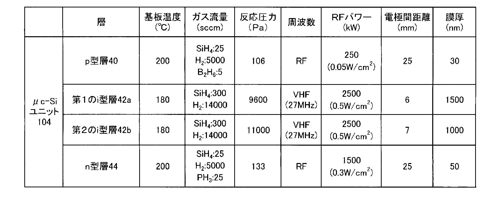
- the p-type layer 40, i-type layer 42, and n-type layer 44 of the ⁇ c-Si unit 104 were formed under the film formation conditions shown in Table 2.
- Diborane (B 2 H 6 ) and phosphine (PH 3 ) have a gas flow rate of 1% on a hydrogen basis.
- the crystallization rate Xc is low near the center in the plane of the substrate, and the uniformity of the crystallization rate Xc is high in the plane of the substrate.
- the first i-type layer 42a formed under the film forming conditions is formed as a single film on the glass substrate, the first i-type layer 42a has a crystallization ratio Xc near the center in the plane of the substrate.
- a laminated structure with the second i-type layer 42b formed under film-forming conditions that is high and the uniformity of the crystallization ratio Xc is lower than that of the first i-type layer 42a in the plane of the substrate.
- the film thickness of the first i-type layer 42a was 1.5 ⁇ m, and the film thickness of the second i-type layer 42b was 1.0 ⁇ m.
- a YAG laser was irradiated to a position 50 ⁇ m lateral from the patterning position of the transparent conductive film 12, and the a-Si unit 102 and the ⁇ c-Si unit 104 were patterned into strips.
- a ZnO film was formed as the first back electrode layer 16 by sputtering, and an Ag electrode was formed as the second back electrode layer 18 by sputtering.
- a YAG laser was irradiated to a position 50 ⁇ m lateral from the patterning position of the a-Si unit 102 and the ⁇ c-Si unit 104, and the first back electrode layer 16 and the second back electrode layer 18 were patterned into strips.
- a YAG laser having an energy density of 0.7 J / cm 2 and a pulse frequency of 4 kHz was used.
- Example 2 The film thickness of the first i-type layer 42a was 1.0 ⁇ m and the film thickness of the second i-type layer 42b was 1.5 ⁇ m under the same film formation conditions as in Example 1 above.
- Example 1 Under the same film forming conditions as in Example 1, the thickness of the first i-type layer 42a was 2.5 ⁇ m, and the second i-type layer 42b was not formed.
- Example 2 Under the same film forming conditions as in Example 1, the first i-type layer 42a is not formed, and the second i-type layer 42b has a thickness of 2.5 ⁇ m on the n-type layer of the a-Si unit 102. Directly formed.
- Example 3 (Comparative Example 3) Compared to Example 1, the film formation order of the first i-type layer 42a and the second i-type layer 42b was reversed. That is, the second i-type layer 42b having a thickness of 1.0 ⁇ m is formed on the n-type layer of the a-Si unit 102, and then the first i-type layer 42a having a thickness of 1.5 ⁇ m is formed. did.
- Comparative Example 4 Similar to Comparative Example 3, the film formation order of the first i-type layer 42a and the second i-type layer 42b was reversed.
- the film thickness of the second i-type layer 42b was 1.5 ⁇ m, and the film thickness of the first i-type layer 42a was 1.0 ⁇ m.
- Table 3 shows the open circuit voltage Voc, the short-circuit current density Jsc, the fill factor FF, and the efficiency ⁇ of the photoelectric conversion devices of Examples 1 and 2 and Comparative Examples 1 to 4.
- the photoelectric conversion measurement was performed at 8 points in the center 100 mm ⁇ 100 mm in the panel surface of the photoelectric conversion device and 1 point inside 55 mm from the corner of the panel. An average value is calculated for the eight central points in the panel surface, and the average values of the open circuit voltage Voc, the short circuit current density Jsc, the fill factor FF, and the efficiency ⁇ are normalized to 1 respectively.
- Example 1 the decrease in the short circuit current density Jsc and the fill factor FF is small even near the edge of the panel surface, and the decrease in the photoelectric conversion efficiency ⁇ as a cell is small compared to the value near the center.
- Example 2 the short-circuit current density Jsc is lower than that in Example 1.
- the fill factor FF is improved, and the photoelectric conversion efficiency ⁇ as a cell is lower than the value near the center. small.
- the open-circuit voltage Voc and the fill factor FF are greatly reduced as compared with values near the center.
- the short-circuit current density Jsc was greatly improved, and the decrease in photoelectric conversion efficiency ⁇ as a cell was smaller than the value near the center.
- the absolute value of the efficiency ⁇ of each cell is much lower than in Examples 1 and 2, and it was not possible to satisfy both the improvement of the absolute efficiency ⁇ and the uniformization of the efficiency ⁇ within the panel surface. .
- the open circuit voltage Voc is slightly improved as compared with the value near the center, but the short circuit current
- the density Jsc and the fill factor FF were significantly reduced, and the efficiency ⁇ of photoelectric conversion as a cell was greatly reduced as compared to the value near the center.
- the efficiency ⁇ in the panel surface cannot be made uniform.
- the reason why the above results are obtained is that the first i-type layer 42a having a relatively uniform in-plane crystallization ratio Xc distribution is formed as a base, and the second i formed on the first i-type layer 42a is formed. It can be inferred that the mold layer 42b was able to further increase the crystallization rate Xc as an absolute value while inheriting the uniformity of the crystallization rate Xc of the first i-type layer 42a.
- FIG. 5 shows the crystallization rate Xc of the first i-type layer 42a and the crystallization rate Xc in a state where the second i-type layer 42b is formed on the first i-type layer 42a. The result of having measured the distance from an edge part on the diagonal of this panel is shown.
- the measurement location is cut out and subjected to oblique polishing in the thickness direction to leave only the first i-type layer 42a and the second on the first i-type layer 42a.
- the crystallization rate Xc with the region where the i-type layer 42b is left is measured by Raman spectroscopy.
- the crystallization rate Xc is determined by analyzing a Raman spectrum measured using a laser beam having a wavelength of 514 nm by Raman spectroscopy, and a Raman scattering intensity Ic near 520 cm ⁇ 1 caused by crystalline silicon and 480 cm caused by amorphous silicon. The peak was separated into a peak with a Raman scattering intensity Ia in the vicinity of ⁇ 1 and defined as a ratio Ic / Ia of the peak heights.
- the crystallization rate Xc (bold line in FIG. 5) of only the first i-type layer 42a in the region of 5 to 11 cm from the edge of the panel is the second on the first i-type layer 42a.
- the crystallization rate Xc (the thin line in FIG. 5) when the i-type layer 42b was formed was higher. That is, in the region of 5 cm to 11 cm from the edge of the panel, the change in the film thickness direction of the crystallization rate is measured, and the entire i-type layer 40 (the second i-type layer 42b is formed on the first i-type layer 42a).
- tandem structure of the amorphous silicon photoelectric conversion unit 102 and the microcrystalline silicon photoelectric conversion unit 104 is described as an example; however, the present invention is not limited to this, and the microcrystalline silicon photoelectric conversion unit 104 A single structure may be used, a laminated structure with photoelectric conversion units other than the amorphous silicon photoelectric conversion unit 102, or a laminated structure of three or more photoelectric conversion units.
- the first i-type layer 42 a and the second i-type layer 42 b are formed directly on the p-type layer 40.
- a buffer layer 42c is provided between the p-type layer 40 and the first i-type layer 42a.
- the buffer layer 42c is preferably formed by a plasma film forming method.
- the plasma film forming method it is preferable to apply a VHF plasma film forming method with a frequency of 13.56 MHz to 70 MHz.
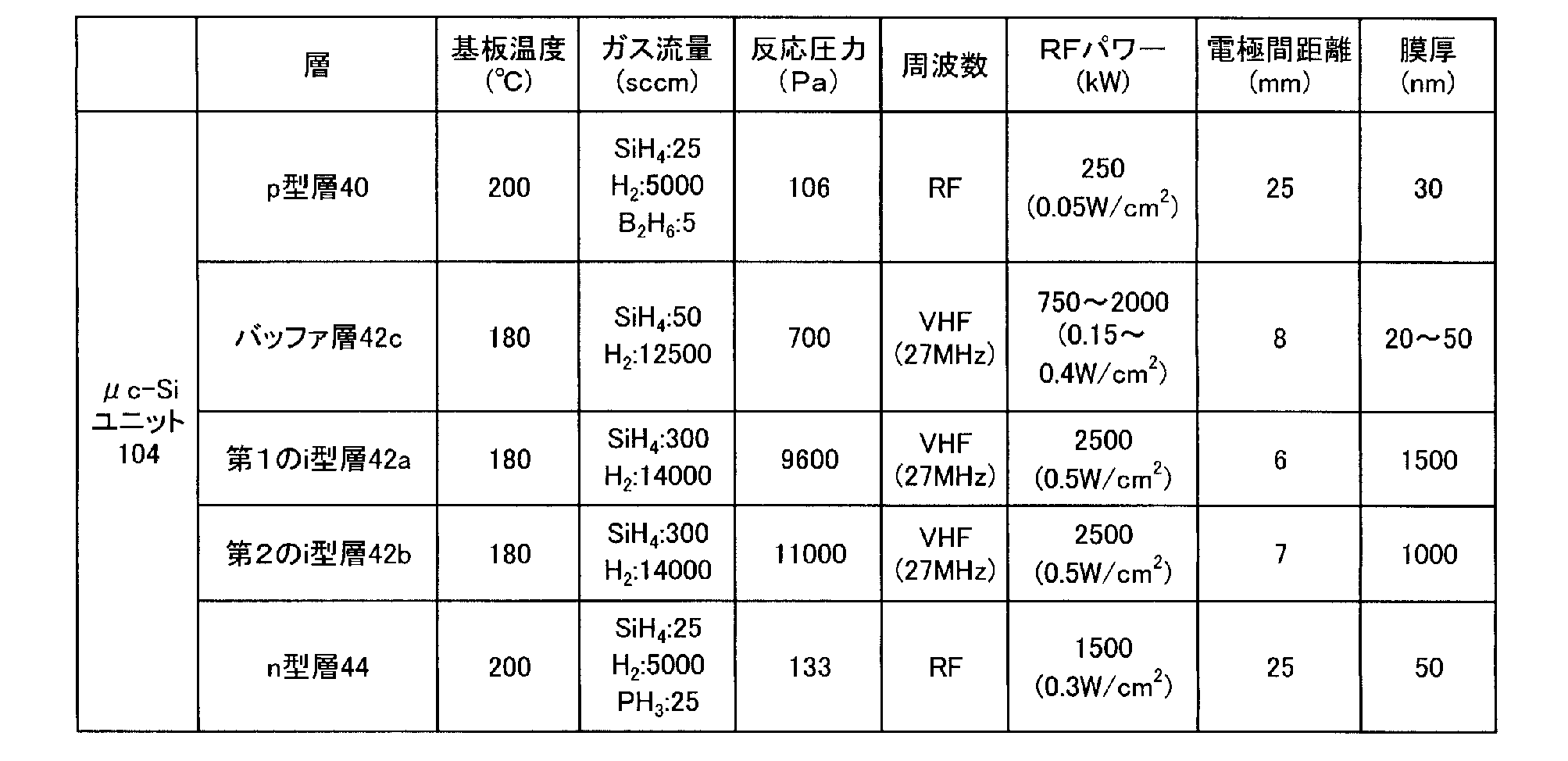
- the substrate temperature during film formation set to 160 ° C. or higher 230 ° C. or less, introducing power to the plasma is preferably set to 0.15 W / cm 2 or more 0.4 W / cm 2 or less.
- the film thickness of the buffer layer 42c is preferably 20 nm or more and 50 nm or less.
- the buffer layer 42c has a crystallization rate Xc when formed as a single film on a glass substrate or the like, and the crystallization of the first i-type layer 42a and the second i-type layer 42b formed as a single film on the glass substrate or the like. It is preferable that the rate is higher than Xc.
- the distribution of the crystallization ratio Xc in the surface of the substrate is the same as that of the first i-type layer 42a and the second i-type layer 42b. It is preferable that the crystallization rate Xc is more uniform than the distribution of the crystallization rate Xc.
- the crystallization rate Xc of the buffer layer 42c is preferably 10 or more, and more preferably 13 or more. At this time, when the crystallization ratio Xc of the buffer layer 42c is 10 or more and less than 13, the thickness of the buffer layer 42c is preferably 40 nm or more. When the crystallization ratio Xc of the buffer layer 42c is 13 or more, the thickness of the buffer layer 42c is not particularly limited, but is preferably 30 nm or more.
- the buffer layer 42c is formed as one of undoped i-type layers, but may be formed as one of p-type layers by adding a p-type dopant.
- Examples 3 to 5 The transparent insulating substrate 10 and the transparent conductive film 12 were prepared in the same manner as in Example 1. After patterning the transparent conductive film 12 into a strip shape, the p-type layer, i-type layer, and n-type layer of the a-Si unit 102 were sequentially laminated under the conditions shown in Table 1 as in Example 1.
- the ⁇ c-Si unit 104 was formed under the conditions shown in Table 4. After forming the p-type layer 40 on the a-Si unit 102, the buffer layer 42c was formed. In the buffer layer 42c, the first i-type layer 42a, the second i-type layer 42b, and the n-type layer 44 were formed as in the first embodiment. In Table 4, diborane (B 2 H 6 ) and phosphine (PH 3 ) are gas flows having a concentration of 1% on a hydrogen basis.
- the film formation conditions shown in Table 4 are as follows: the crystallization rate Xc when the buffer layer 42c is formed as a single film on a glass substrate or the like is the first i-type layer 42a and the second The i-type layer 42b has a higher crystallization rate Xc, and the distribution of the crystallization rate Xc in the plane of the substrate when the buffer layer 42c is formed as a single film on a glass substrate or the like is the first i-type layer 42a.
- the second i-type layer 42b is more uniform than the distribution of the crystallization rate Xc when the second i-type layer 42b is formed as a single film on a glass substrate or the like.
- Example 2 Thereafter, similarly to Example 1, the a-Si unit 102 and the ⁇ c-Si unit 104 were patterned into strips, and the first back electrode layer 16 and the second back electrode layer 18 were formed by sputtering. Furthermore, the 1st back surface electrode layer 16 and the 2nd back surface electrode layer 18 were patterned in strip shape.
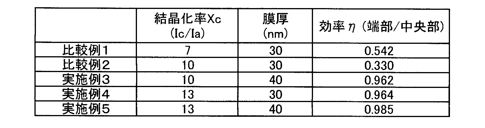
- Example 3 a sample formed to have a film thickness of 40 nm under the condition that the crystallization rate Xc (Ic / Ia) is 10 when the buffer layer 42c is formed as a single film on a glass substrate or the like is described as Example 3. did. Further, a sample formed so as to have a film thickness of 30 nm under the condition that the crystallization rate Xc (Ic / Ia) is 13 is obtained under the condition that the crystallization rate Xc (Ic / Ia) is 13 in Example 4. A sample formed to have a film thickness of 40 nm was taken as Example 5. The crystallization ratio Xc of the buffer layer 42c can be adjusted by changing the power introduced into the plasma during film formation. The film thickness of the first i-type layer 42a was 1.5 ⁇ m, and the film thickness of the second i-type layer 42b was 1.0 ⁇ m.
- Comparative Examples 5 and 6 A sample in which the buffer layer 42c was formed to a thickness of 30 nm under the condition that the crystallization ratio Xc (Ic / Ia) when the buffer layer 42c was formed as a single film on a glass substrate or the like was set as Comparative Example 5. Further, a sample formed to have a film thickness of 30 nm under the condition that the crystallization ratio Xc (Ic / Ia) was 10 was set as Comparative Example 6.
- Table 4 and FIG. 7 show the distribution of efficiency ⁇ with respect to the position on the substrate surface in Example 5.
- FIG. 7 also shows the results of a comparative example formed under the same conditions as in Example 5 except that the buffer layer 42c is not formed. Further, the efficiency ⁇ indicates a value normalized by a value at the center of the substrate.
- the efficiency ⁇ is reduced to 0.85 times that of the center of the substrate at the substrate end, whereas the buffer layer 42c is formed.
- the efficiency ⁇ at the end of the substrate was almost 0.99 times lower than that at the center of the substrate.
- Table 6 and FIG. 8 show the results of measuring the substrate edge efficiency ⁇ for Comparative Examples 5 and 6 and Example 3-5. Also in Table 6 and FIG. 8, as in FIG. 7, the efficiency ⁇ indicates a value normalized with the value at the center of the substrate.
- the efficiency ⁇ is maintained at 0.962 to 0.985 times at the substrate end portion relative to the center portion of the substrate, and the photoelectric conversion efficiency in the panel plane of the photoelectric conversion device is maintained. The effect of reducing dispersion was observed. On the other hand, in the samples of Comparative Examples 5 and 6, the efficiency ⁇ decreased to 0.542 times and 0.330 times at the substrate end portion with respect to the center portion of the substrate.
- the crystallization rate Xc is higher than that of the first i-type layer 42a and the second i-type layer 42b.
- the buffer layer 42c has a remarkable effect when the crystallization rate Xc (Ic / Ia) is 10 or more and the film thickness is 40 nm or more, or when the crystallization rate Xc (Ic / Ia) is 13 or more.
Landscapes
- Chemical & Material Sciences (AREA)
- General Chemical & Material Sciences (AREA)
- Chemical Kinetics & Catalysis (AREA)
- Engineering & Computer Science (AREA)
- Materials Engineering (AREA)
- Mechanical Engineering (AREA)
- Metallurgy (AREA)
- Organic Chemistry (AREA)
- Inorganic Chemistry (AREA)
- Photovoltaic Devices (AREA)
- Chemical Vapour Deposition (AREA)
- Solid State Image Pick-Up Elements (AREA)
Abstract
Description
以下、本発明の実施例及び比較例を示す。
透明絶縁基板10として、550mm×650mm角,4mm厚のガラス基板を用いた。透明絶縁基板10上に、熱CVDにより透明導電膜12として表面に凹凸形状を有する600nm厚のSnO2を形成した。この後、透明導電膜12をYAGレーザにて短冊状にパターニングした。YAGレーザは、波長1064nm、エネルギー密度13J/cm2、パルス周波数3kHzのものを用いた。

上記実施例1と同様の成膜条件で、第1のi型層42aの膜厚を1.0μmとし、第2のi型層42bの膜厚を1.5μmとした。
上記実施例1と同様の成膜条件で、第1のi型層42aの膜厚を2.5μmとし、第2のi型層42bを形成しなかった。
上記実施例1と同様の成膜条件で、第1のi型層42aを形成せず、第2のi型層42bの膜厚を2.5μmとしてa-Siユニット102のn型層上に直接形成した。
上記実施例1に対して、第1のi型層42aと第2のi型層42bの成膜順を逆にした。すなわち、a-Siユニット102のn型層上に膜厚1.0μmの第2のi型層42bを先に形成し、次に膜厚を1.5μmの第1のi型層42aを形成した。
比較例3と同様に、第1のi型層42aと第2のi型層42bの成膜順を逆にした。第2のi型層42bの膜厚を1.5μmとし、第1のi型層42aの膜厚を1.0μmとした。

透明絶縁基板10及び透明導電膜12については実施例1と同様に準備した。透明導電膜12を短冊状にパターニングした後、実施例1と同様に、表1に示した条件でa-Siユニット102のp型層,i型層及びn型層を順に積層した。
バッファ層42cをガラス基板等に単膜として成膜したときの結晶化率Xc(Ic/Ia)が7となる条件で膜厚30nmとなるように成膜した試料を比較例5とした。また、結晶化率Xc(Ic/Ia)が10となる条件で膜厚30nmとなるように成膜した試料を比較例6とした。

Claims (8)
- p型層、発電層となる微結晶シリコン層を含むi型層、n型層の積層構造を備えた光電変換装置の製造方法において、
前記i型層を形成する工程であって、第1の微結晶シリコン層を形成し、前記第1の微結晶シリコン層上に、前記第1の微結晶シリコン層より結晶化率が高く、結晶化率の面内分布が低くなる条件で第2の微結晶シリコン層を形成する工程を含むことを特徴とする光電変換装置の製造方法。 - 請求項1に記載の光電変換装置の製造方法であって、
前記第1の微結晶シリコン層は、ガラス基板に単膜として成膜した場合に、ラマン分光法における520cm-1付近のラマン散乱強度Icと480cm-1付近のラマン散乱強度Iaとのピーク高さの比Ic/Iaが2~4の範囲となる条件で形成され、
前記第2の微結晶シリコン層は、ガラス基板に単膜として成膜した場合に、前記ピーク高さの比Ic/Iaが4~6の範囲となる条件で形成されることを特徴とする光電変換装置の製造方法。 - 請求項1又は2に記載の光電変換装置の製造方法であって、
前記第1の微結晶シリコン層を形成する前に、前記第1の微結晶シリコン層及び前記第2の微結晶シリコン層より結晶化率が高く、結晶化率の面内分布が高くなる条件でバッファ層を形成する工程をさらに含むことを特徴とする光電変換装置の製造方法。 - 請求項3に記載の光電変換装置の製造方法であって、
前記バッファ層は、ガラス基板に単膜として成膜した場合に、ラマン分光法における520cm-1付近のラマン散乱強度Icと480cm-1付近のラマン散乱強度Iaとのピーク高さの比Ic/Iaが10以上及びその膜厚が40nm以上、又は、前記ピーク高さの比Ic/Iaが13以上とすることを特徴とする光電変換装置の製造方法。 - p型ドーパントを含むp型層、発電層となる微結晶シリコン層を含むi型層、n型ドーパントを含むn型層の積層構造を備えた光電変換装置において、
前記i型層は、第1の微結晶シリコン層と、前記第1の微結晶シリコン層より結晶化率が高く、結晶化率の面内分布が低くなる条件で形成された第2の微結晶シリコン層と、の積層構造を有することを特徴とする光電変換装置。 - 請求項5に記載の光電変換装置であって、
前記第1の微結晶シリコン層は、その膜厚が100nm以上2500nm以下の範囲であることを特徴とする光電変換装置。 - 請求項5又は6に記載の光電変換装置であって、
前記第1の微結晶シリコン層及び前記第2の微結晶シリコン層より結晶化率が高く、結晶化率の面内分布が高くなる条件で形成されたバッファ層をさらに備え、
前記バッファ層上に前記第1の微結晶シリコン層が形成されていることを特徴とする光電変換装置の製造方法。 - 請求項7に記載の光電変換装置であって、
前記バッファ層は、ガラス基板に単膜として成膜した場合に、ラマン分光法における520cm-1付近のラマン散乱強度Icと480cm-1付近のラマン散乱強度Iaとのピーク高さの比Ic/Iaが10以上及びその膜厚が40nm以上、又は、前記ピーク高さの比Ic/Iaが13以上であることを特徴とする光電変換装置。
Priority Applications (3)
| Application Number | Priority Date | Filing Date | Title |
|---|---|---|---|
| US13/391,570 US20120145239A1 (en) | 2009-11-30 | 2010-11-24 | Photoelectric converter and method for producing same |
| EP10833189.3A EP2458644A4 (en) | 2009-11-30 | 2010-11-24 | PHOTOELECTRIC CONVERTER AND METHOD FOR THE PRODUCTION THEREOF |
| CN2010800358789A CN102473759A (zh) | 2009-11-30 | 2010-11-24 | 光电转换装置和其制造方法 |
Applications Claiming Priority (4)
| Application Number | Priority Date | Filing Date | Title |
|---|---|---|---|
| JP2009272011 | 2009-11-30 | ||
| JP2009-272011 | 2009-11-30 | ||
| JP2010-253550 | 2010-11-12 | ||
| JP2010253550A JP4902779B2 (ja) | 2009-11-30 | 2010-11-12 | 光電変換装置及びその製造方法 |
Publications (1)
| Publication Number | Publication Date |
|---|---|
| WO2011065343A1 true WO2011065343A1 (ja) | 2011-06-03 |
Family
ID=44066448
Family Applications (1)
| Application Number | Title | Priority Date | Filing Date |
|---|---|---|---|
| PCT/JP2010/070853 Ceased WO2011065343A1 (ja) | 2009-11-30 | 2010-11-24 | 光電変換装置及びその製造方法 |
Country Status (6)
| Country | Link |
|---|---|
| US (1) | US20120145239A1 (ja) |
| EP (1) | EP2458644A4 (ja) |
| JP (1) | JP4902779B2 (ja) |
| KR (1) | KR20120042894A (ja) |
| CN (1) | CN102473759A (ja) |
| WO (1) | WO2011065343A1 (ja) |
Cited By (1)
| Publication number | Priority date | Publication date | Assignee | Title |
|---|---|---|---|---|
| WO2013065538A1 (ja) * | 2011-11-03 | 2013-05-10 | 三洋電機株式会社 | 光電変換装置 |
Families Citing this family (8)
| Publication number | Priority date | Publication date | Assignee | Title |
|---|---|---|---|---|
| WO2013022086A1 (ja) * | 2011-08-11 | 2013-02-14 | 株式会社カネカ | 積層型光電変換装置の製造方法 |
| KR101770266B1 (ko) * | 2011-09-15 | 2017-08-22 | 엘지전자 주식회사 | 박막 태양전지 모듈 |
| KR101770267B1 (ko) * | 2011-10-04 | 2017-08-22 | 엘지전자 주식회사 | 박막 태양전지 모듈 |
| WO2013080803A1 (ja) * | 2011-11-30 | 2013-06-06 | 三洋電機株式会社 | 光起電力装置 |
| KR101302373B1 (ko) | 2011-12-21 | 2013-09-06 | 주식회사 테스 | 태양전지 제조방법 |
| KR101453967B1 (ko) * | 2012-02-20 | 2014-10-29 | 고려대학교 산학협력단 | 다중 밴드갭 적층형 태양전지 및 다중 밴드갭 적층형 태양전지 형성 방법 |
| TWI469380B (zh) * | 2013-11-08 | 2015-01-11 | Ind Tech Res Inst | 異質接面太陽電池結構 |
| WO2017195722A1 (ja) * | 2016-05-09 | 2017-11-16 | 株式会社カネカ | 積層型光電変換装置およびその製造方法 |
Citations (4)
| Publication number | Priority date | Publication date | Assignee | Title |
|---|---|---|---|---|
| JPH11251612A (ja) * | 1998-03-03 | 1999-09-17 | Canon Inc | 光起電力素子の製造方法 |
| JP2000349321A (ja) * | 1999-06-09 | 2000-12-15 | Fuji Electric Co Ltd | 薄膜太陽電池とその製造方法 |
| JP2004363578A (ja) * | 2003-05-13 | 2004-12-24 | Kyocera Corp | 半導体薄膜およびそれを用いた光電変換装置ならびに光発電装置 |
| WO2009119124A1 (ja) * | 2008-03-28 | 2009-10-01 | 三菱重工業株式会社 | 光電変換装置 |
Family Cites Families (7)
| Publication number | Priority date | Publication date | Assignee | Title |
|---|---|---|---|---|
| JP2984537B2 (ja) * | 1994-03-25 | 1999-11-29 | キヤノン株式会社 | 光起電力素子 |
| JP4208281B2 (ja) * | 1998-02-26 | 2009-01-14 | キヤノン株式会社 | 積層型光起電力素子 |
| JP2004165394A (ja) * | 2002-11-13 | 2004-06-10 | Canon Inc | 積層型光起電力素子 |
| DE102004061360A1 (de) * | 2004-12-21 | 2006-07-13 | Forschungszentrum Jülich GmbH | Verfahren zur Herstellung einer Dünnschichtsolarzelle mit mikrokristallinem Silizium sowie Schichtfolge |
| JP5309426B2 (ja) * | 2006-03-29 | 2013-10-09 | 株式会社Ihi | 微結晶シリコン膜形成方法及び太陽電池 |
| JP5473187B2 (ja) * | 2006-09-04 | 2014-04-16 | 三菱重工業株式会社 | 製膜条件設定方法、光電変換装置の製造方法及び検査方法 |
| US8288647B2 (en) * | 2006-12-25 | 2012-10-16 | Sharp Kabushiki Kaisha | Photoelectric conversion device and method of producing the same |
-
2010
- 2010-11-12 JP JP2010253550A patent/JP4902779B2/ja not_active Expired - Fee Related
- 2010-11-24 WO PCT/JP2010/070853 patent/WO2011065343A1/ja not_active Ceased
- 2010-11-24 KR KR1020127002699A patent/KR20120042894A/ko not_active Abandoned
- 2010-11-24 EP EP10833189.3A patent/EP2458644A4/en not_active Withdrawn
- 2010-11-24 CN CN2010800358789A patent/CN102473759A/zh active Pending
- 2010-11-24 US US13/391,570 patent/US20120145239A1/en not_active Abandoned
Patent Citations (4)
| Publication number | Priority date | Publication date | Assignee | Title |
|---|---|---|---|---|
| JPH11251612A (ja) * | 1998-03-03 | 1999-09-17 | Canon Inc | 光起電力素子の製造方法 |
| JP2000349321A (ja) * | 1999-06-09 | 2000-12-15 | Fuji Electric Co Ltd | 薄膜太陽電池とその製造方法 |
| JP2004363578A (ja) * | 2003-05-13 | 2004-12-24 | Kyocera Corp | 半導体薄膜およびそれを用いた光電変換装置ならびに光発電装置 |
| WO2009119124A1 (ja) * | 2008-03-28 | 2009-10-01 | 三菱重工業株式会社 | 光電変換装置 |
Cited By (1)
| Publication number | Priority date | Publication date | Assignee | Title |
|---|---|---|---|---|
| WO2013065538A1 (ja) * | 2011-11-03 | 2013-05-10 | 三洋電機株式会社 | 光電変換装置 |
Also Published As
| Publication number | Publication date |
|---|---|
| JP4902779B2 (ja) | 2012-03-21 |
| JP2011135053A (ja) | 2011-07-07 |
| CN102473759A (zh) | 2012-05-23 |
| US20120145239A1 (en) | 2012-06-14 |
| KR20120042894A (ko) | 2012-05-03 |
| EP2458644A4 (en) | 2013-04-10 |
| EP2458644A1 (en) | 2012-05-30 |
Similar Documents
| Publication | Publication Date | Title |
|---|---|---|
| JP4902779B2 (ja) | 光電変換装置及びその製造方法 | |
| JP4940290B2 (ja) | 光電変換装置及びその製造方法 | |
| JP4767365B2 (ja) | 薄膜太陽電池及びその製造方法 | |
| JP2010283161A (ja) | 太陽電池及びその製造方法 | |
| US8759667B2 (en) | Photoelectric conversion device | |
| JP4712127B2 (ja) | 太陽電池の製造方法及び製造装置 | |
| JPWO2013168515A1 (ja) | 光電変換装置およびその製造方法 | |
| JP2011014619A (ja) | 太陽電池及びその製造方法 | |
| JP2008283075A (ja) | 光電変換装置の製造方法 | |
| JP2011014618A (ja) | 太陽電池及びその製造方法 | |
| JP2010283162A (ja) | 太陽電池及びその製造方法 | |
| JP5373045B2 (ja) | 光電変換装置 | |
| JP2011060811A (ja) | 太陽電池モジュール及びその製造方法 | |
| WO2011105166A1 (ja) | 光電変換モジュール及びその製造方法 | |
| US20100307573A1 (en) | Solar cell and manufacturing method thereof | |
| WO2011148724A1 (ja) | 積層型光電変換装置用中間層、積層型光電変換装置および積層型光電変換装置の製造方法 | |
| JP2011216586A (ja) | 積層型光電変換装置および積層型光電変換装置の製造方法 | |
| US20100330734A1 (en) | Solar cell and manufacturing method thereof | |
| JP2011077220A (ja) | 太陽電池 | |
| JP2011014617A (ja) | 太陽電池及びその製造方法 | |
| JP2013026602A (ja) | 光電変換装置 | |
| WO2013080803A1 (ja) | 光起電力装置 | |
| WO2010146846A1 (ja) | 光電変換装置及び光電変換装置の製造方法 | |
| JP2010283159A (ja) | 太陽電池及びその製造方法 | |
| WO2013125251A1 (ja) | 薄膜太陽電池 |
Legal Events
| Date | Code | Title | Description |
|---|---|---|---|
| WWE | Wipo information: entry into national phase |
Ref document number: 201080035878.9 Country of ref document: CN |
|
| 121 | Ep: the epo has been informed by wipo that ep was designated in this application |
Ref document number: 10833189 Country of ref document: EP Kind code of ref document: A1 |
|
| ENP | Entry into the national phase |
Ref document number: 20127002699 Country of ref document: KR Kind code of ref document: A |
|
| WWE | Wipo information: entry into national phase |
Ref document number: 2010833189 Country of ref document: EP |
|
| WWE | Wipo information: entry into national phase |
Ref document number: 13391570 Country of ref document: US |
|
| NENP | Non-entry into the national phase |
Ref country code: DE |