WO2011074334A1 - 照明装置、表示装置、及びテレビ受信装置 - Google Patents
照明装置、表示装置、及びテレビ受信装置 Download PDFInfo
- Publication number
- WO2011074334A1 WO2011074334A1 PCT/JP2010/069270 JP2010069270W WO2011074334A1 WO 2011074334 A1 WO2011074334 A1 WO 2011074334A1 JP 2010069270 W JP2010069270 W JP 2010069270W WO 2011074334 A1 WO2011074334 A1 WO 2011074334A1
- Authority
- WO
- WIPO (PCT)
- Prior art keywords
- light
- sheet
- chassis
- boundary line
- led
- Prior art date
- Legal status (The legal status is an assumption and is not a legal conclusion. Google has not performed a legal analysis and makes no representation as to the accuracy of the status listed.)
- Ceased
Links
Images



Classifications
-
- G—PHYSICS
- G02—OPTICS
- G02F—OPTICAL DEVICES OR ARRANGEMENTS FOR THE CONTROL OF LIGHT BY MODIFICATION OF THE OPTICAL PROPERTIES OF THE MEDIA OF THE ELEMENTS INVOLVED THEREIN; NON-LINEAR OPTICS; FREQUENCY-CHANGING OF LIGHT; OPTICAL LOGIC ELEMENTS; OPTICAL ANALOGUE/DIGITAL CONVERTERS
- G02F1/00—Devices or arrangements for the control of the intensity, colour, phase, polarisation or direction of light arriving from an independent light source, e.g. switching, gating or modulating; Non-linear optics
- G02F1/01—Devices or arrangements for the control of the intensity, colour, phase, polarisation or direction of light arriving from an independent light source, e.g. switching, gating or modulating; Non-linear optics for the control of the intensity, phase, polarisation or colour
- G02F1/13—Devices or arrangements for the control of the intensity, colour, phase, polarisation or direction of light arriving from an independent light source, e.g. switching, gating or modulating; Non-linear optics for the control of the intensity, phase, polarisation or colour based on liquid crystals, e.g. single liquid crystal display cells
- G02F1/133—Constructional arrangements; Operation of liquid crystal cells; Circuit arrangements
- G02F1/1333—Constructional arrangements; Manufacturing methods
- G02F1/1335—Structural association of cells with optical devices, e.g. polarisers or reflectors
- G02F1/1336—Illuminating devices
- G02F1/133602—Direct backlight
- G02F1/133603—Direct backlight with LEDs
-
- G—PHYSICS
- G02—OPTICS
- G02F—OPTICAL DEVICES OR ARRANGEMENTS FOR THE CONTROL OF LIGHT BY MODIFICATION OF THE OPTICAL PROPERTIES OF THE MEDIA OF THE ELEMENTS INVOLVED THEREIN; NON-LINEAR OPTICS; FREQUENCY-CHANGING OF LIGHT; OPTICAL LOGIC ELEMENTS; OPTICAL ANALOGUE/DIGITAL CONVERTERS
- G02F1/00—Devices or arrangements for the control of the intensity, colour, phase, polarisation or direction of light arriving from an independent light source, e.g. switching, gating or modulating; Non-linear optics
- G02F1/01—Devices or arrangements for the control of the intensity, colour, phase, polarisation or direction of light arriving from an independent light source, e.g. switching, gating or modulating; Non-linear optics for the control of the intensity, phase, polarisation or colour
- G02F1/13—Devices or arrangements for the control of the intensity, colour, phase, polarisation or direction of light arriving from an independent light source, e.g. switching, gating or modulating; Non-linear optics for the control of the intensity, phase, polarisation or colour based on liquid crystals, e.g. single liquid crystal display cells
- G02F1/133—Constructional arrangements; Operation of liquid crystal cells; Circuit arrangements
- G02F1/1333—Constructional arrangements; Manufacturing methods
- G02F1/1335—Structural association of cells with optical devices, e.g. polarisers or reflectors
- G02F1/1336—Illuminating devices
- G02F1/133602—Direct backlight
- G02F1/133605—Direct backlight including specially adapted reflectors
-
- G—PHYSICS
- G09—EDUCATION; CRYPTOGRAPHY; DISPLAY; ADVERTISING; SEALS
- G09F—DISPLAYING; ADVERTISING; SIGNS; LABELS OR NAME-PLATES; SEALS
- G09F9/00—Indicating arrangements for variable information in which the information is built-up on a support by selection or combination of individual elements
- G09F9/30—Indicating arrangements for variable information in which the information is built-up on a support by selection or combination of individual elements in which the desired character or characters are formed by combining individual elements
- G09F9/35—Indicating arrangements for variable information in which the information is built-up on a support by selection or combination of individual elements in which the desired character or characters are formed by combining individual elements being liquid crystals
-
- G—PHYSICS
- G02—OPTICS
- G02F—OPTICAL DEVICES OR ARRANGEMENTS FOR THE CONTROL OF LIGHT BY MODIFICATION OF THE OPTICAL PROPERTIES OF THE MEDIA OF THE ELEMENTS INVOLVED THEREIN; NON-LINEAR OPTICS; FREQUENCY-CHANGING OF LIGHT; OPTICAL LOGIC ELEMENTS; OPTICAL ANALOGUE/DIGITAL CONVERTERS
- G02F1/00—Devices or arrangements for the control of the intensity, colour, phase, polarisation or direction of light arriving from an independent light source, e.g. switching, gating or modulating; Non-linear optics
- G02F1/01—Devices or arrangements for the control of the intensity, colour, phase, polarisation or direction of light arriving from an independent light source, e.g. switching, gating or modulating; Non-linear optics for the control of the intensity, phase, polarisation or colour
- G02F1/13—Devices or arrangements for the control of the intensity, colour, phase, polarisation or direction of light arriving from an independent light source, e.g. switching, gating or modulating; Non-linear optics for the control of the intensity, phase, polarisation or colour based on liquid crystals, e.g. single liquid crystal display cells
- G02F1/133—Constructional arrangements; Operation of liquid crystal cells; Circuit arrangements
- G02F1/1333—Constructional arrangements; Manufacturing methods
- G02F1/1335—Structural association of cells with optical devices, e.g. polarisers or reflectors
- G02F1/1336—Illuminating devices
- G02F1/133602—Direct backlight
- G02F1/133611—Direct backlight including means for improving the brightness uniformity
Definitions
- the present invention relates to a lighting device, a display device, and a television receiver.
- a liquid crystal panel used for a liquid crystal display device such as a liquid crystal television does not emit light spontaneously, and therefore requires a backlight device as a separate illumination device.
- This backlight device is well known to be installed on the back side of the liquid crystal panel (opposite to the display surface).
- the backlight device is installed on the inner surface of the bottom plate of the chassis and the chassis having a shape opened on the liquid crystal panel side.
- a plurality of light sources for example, cold cathode tubes and LEDs
- a light reflection sheet that is laid in the chassis and reflects light from the light sources toward the liquid crystal panel.
- the light reflecting sheet laid on the backlight device described above includes a sheet bottom portion arranged along the bottom plate of the chassis, a sheet inclined portion extending from a peripheral portion of the sheet bottom portion, and inclined toward the liquid crystal panel with respect to the sheet bottom portion. It is composed of More specifically, the sheet inclined portion is inclined so as to approach the liquid crystal panel as it goes to the outside of the chassis. By this sheet inclined portion, it is possible to direct the reflected light to the inner side (center side of the liquid crystal display device).
- the optical axis of the light source is arranged on the bottom plate in a direction toward the liquid crystal panel (that is, the light source is arranged at a position corresponding to the bottom of the light reflecting sheet).
- the vicinity of the boundary line between the sheet bottom portion and the sheet inclined portion in the light reflecting sheet tends to be a dark portion as compared with the peripheral portion.
- the first reason is that the vicinity of the boundary line corresponds to the peripheral edge of the sheet bottom, and therefore the distance from the light source is longer than the center of the sheet bottom. As a result, the amount of light that reaches the vicinity of the boundary line is relatively small compared to the center side of the sheet bottom.
- the second reason is that, in general, in a light source with high directivity, the light emission amount varies depending on the inclination angle with respect to the optical axis, and the light emission amount decreases as the inclination angle increases.
- the inclination angle with respect to the optical axis of the light source increases on the base end side of the sheet inclined portion, The amount of light reaching the proximal end is relatively small.
- the amount of light that reaches the boundary between the sheet bottom portion and the sheet inclined portion of the light reflecting sheet is relatively small, and the amount of reflected light that is reflected toward the liquid crystal panel is small.
- a darker portion dark portion
- luminance unevenness occurs.
- the present invention has been completed based on the above circumstances, and an object thereof is to provide a lighting device capable of suppressing luminance unevenness. Moreover, it aims at providing the display apparatus provided with such an illuminating device, and a television receiver.
- the present invention includes a light source, a chassis in which the light source is accommodated, and a light reflection sheet that is disposed on an inner surface side of the chassis and can reflect light from the light source, and the light source includes a bottom plate of the chassis.
- the light reflecting sheet includes a sheet bottom portion extending along a surface of the bottom plate, and a sheet inclined portion extending from a peripheral edge of the sheet bottom portion, and the sheet inclined portion is formed on the sheet bottom portion.
- the boundary portion including is set higher than the light reflectance of the adjacent side portion adjacent to the boundary portion on the side farther than the boundary line.
- the light reflectance of the boundary portion along the boundary line between the sheet bottom portion and the sheet inclined portion is set to be higher than the light reflectance of the separated adjacent portion adjacent to the boundary portion. If the light reflectance is set high, the amount of reflected light increases and the brightness increases. With such a configuration, the luminance of the boundary portion where the light emitted from the light source is relatively difficult to reach (that is, the portion where the luminance is likely to decrease when the light reflectance is constant) It can suppress that it becomes low compared with the brightness
- the light-reflecting sheet may be set so that the light reflectance decreases on the surface on the light source side as the distance from the boundary line increases.
- a light reflecting portion set with a light reflectance lower than the light reflectance of the light reflecting sheet may be formed in the separation side adjacent portion.
- the light reflecting portion having a higher light reflectance is provided at the boundary portion.
- a configuration to be formed is also conceivable.
- the light reflecting sheet is set with a high light reflectance in order to increase the light utilization efficiency. For this reason, it is difficult to set only the light reflectance of the boundary portion higher (than the adjacent side portion) on the light reflection sheet originally set with a high light reflectance.
- this invention it was set as the structure which reduces the light reflectivity of a separation side adjacent part by forming the light reflection part of the light reflectance lower than the light reflectivity of a light reflection sheet in a separation side adjacent part. .
- the structure which makes the light reflectivity of a boundary part high with respect to the light reflectivity of a separation side adjacent part is easily realizable.
- the light reflecting portion can be constituted by a dot pattern. If the light reflecting portion is configured by a dot pattern, the light reflectance of the light reflecting portion (and hence the adjacent side portion) can be easily set by setting the mode (area, arrangement interval, etc.) of each dot. It becomes possible.
- the boundary line between the seat bottom and the seat inclined portion may be non-linear in a plan view. In this way, even if the region (boundary part) along the boundary line becomes a dark part, the dark part is non-linear in plan view. If the dark part is non-linear, the boundary between the dark part and the peripheral part thereof is blurred as compared with the case where the dark part is formed in a straight line.
- the boundary line is non-linear means that the boundary line between the seat bottom portion and the seat inclined portion is not linear over the entire length. In other words, a part having a linear shape may be included in a part of the boundary line.
- the boundary line between the seat bottom and the seat inclined portion may have a rectangular wave shape in plan view. If the boundary line has a rectangular wave shape, it is easier to form the boundary line than other non-linear shapes (for example, a sinusoidal curve). Also, if the boundary line is to be formed with a curved line, the inclined surface of the sheet inclined portion also has a curved surface shape, which may cause uneven brightness. In this respect, if the boundary line has a rectangular wave shape, the inclined surface of the sheet inclined portion can be configured only by a flat surface, and therefore, there is no concern that luminance unevenness occurs due to the above-described cause.
- the sheet bottom portion may have a substantially rectangular shape in a plan view, and the sheet inclined portion may extend from four sides around the sheet bottom portion.
- a light emitting diode can be exemplified as the light source. Power consumption can be reduced by using a light emitting diode.
- a diffusing lens arranged so as to cover the light source and capable of diffusing light from the light source.
- the light from the light source is diffused by the diffusion lens.
- a plurality of the light sources may be arranged in a matrix in a direction along the bottom plate of the chassis.
- a display device of the present invention includes the above-described illumination device and a display panel that performs display using light from the illumination device.
- a liquid crystal panel can be exemplified as the display panel.
- Such a display device can be applied as a liquid crystal display device to various uses, for example, a desktop screen of a television or a personal computer, and is particularly suitable for a large screen.
- a television receiver includes the display device.
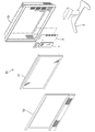
- the disassembled perspective view which shows schematic structure of the television receiver which concerns on Embodiment 1 of this invention.
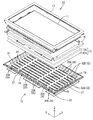
- the disassembled perspective view which shows schematic structure of the liquid crystal display device with which the television receiver of FIG. 1 is provided.
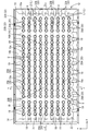
- the top view which shows the backlight apparatus with which the liquid crystal display device of FIG. 2 is provided.
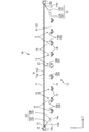
- Sectional drawing which shows the cross-sectional structure along the long side direction of the liquid crystal display device of FIG. 2 (iv-iv line sectional drawing of FIG. 3).
- Sectional drawing which shows the cross-sectional structure along the short side direction of the liquid crystal display device of FIG. 2 (vv line sectional drawing of FIG. 3).
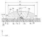
- the expanded sectional view which expanded the LED periphery in FIG.
- the expanded sectional view which shows the emitted light from LED.
- FIGS. 1 A first embodiment of the present invention will be described with reference to FIGS.
- the liquid crystal display device 10 is illustrated.
- the X axis, the Y axis, and the Z axis are drawn in a part of each drawing, and the drawing is such that the directions of the respective axes are the same in each drawing.
- the upper side shown in FIG.4 and FIG.5 be a front side, and let the lower side of the figure be a back side.
- the television receiver TV includes a liquid crystal display device 10, front and back cabinets Ca and Cb that are accommodated so as to sandwich the liquid crystal display device 10, a power source P, a tuner T, And a stand S.
- the liquid crystal display device 10 (display device) has a horizontally long rectangular shape (rectangular shape) as a whole, and is accommodated in a vertically placed state.
- the liquid crystal display device 10 includes a liquid crystal panel 11 that is a display panel and a backlight device 12 (illumination device) that is an external light source, which are integrated by a frame-like bezel 13 or the like. Is supposed to be retained.
- the screen size is 42 inches and the aspect ratio is 16: 9.
- the liquid crystal panel 11 (display panel) has a rectangular shape in plan view, and a pair of glass substrates are bonded together with a predetermined gap therebetween, and liquid crystal is sealed between the glass substrates. It is said.
- One glass substrate is provided with a switching element (for example, TFT) connected to a source wiring and a gate wiring orthogonal to each other, a pixel electrode connected to the switching element, an alignment film, and the like.
- the substrate is provided with a color filter and counter electrodes in which colored portions such as R (red), G (green), and B (blue) are arranged in a predetermined arrangement, and an alignment film.
- polarizing plates 11A and 11B are disposed on the outer sides of both glass substrates (see FIG. 7).
- the backlight device 12 is a so-called direct-type backlight device in which a plurality of LED units U are provided directly below the back surface of the panel surface (display surface) of the liquid crystal panel 11. As shown in FIG. 2, the backlight device 12 covers a substantially box-shaped chassis 14 having an opening 14 b on the light emitting surface side (the liquid crystal panel 11 side), and covers the opening 14 b of the chassis 14.
- optical members arranged (diffusing plate 15a and a plurality of optical sheets 15b arranged between the diffusing plate 15a and the liquid crystal panel 11), the outer edge of the optical member 15 group arranged along the outer edge of the chassis 14
- a frame 16 that holds the portion sandwiched between the chassis 14 and a chassis light reflecting sheet 22 that is disposed on the inner surface side of the chassis 14 and can reflect the light in the chassis 14 toward the optical member 15 side.
- LED units U light source units
- LEDs 17 Light Emitting Diodes
- a holding member 20 is provided in the backlight device 12
- the optical member 15 side (front side) from the LED unit U is the light emitting side.
- the chassis 14 is made of metal and, as shown in FIGS. 3 to 5, has a rectangular bottom plate 14a similar to the liquid crystal panel 11, a side plate 14c rising from an outer end of each side of the bottom plate 14a, and each side plate 14c. And a receiving plate 14d projecting outward from the rising edge, and as a whole, has a shallow substantially box shape (substantially shallow dish shape) opened toward the front side.
- the long side direction of the chassis 14 coincides with the X-axis direction (horizontal direction), and the short side direction coincides with the Y-axis direction (vertical direction).
- a frame 16 and an optical member 15 to be described below can be placed on each receiving plate 14d in the chassis 14 from the front side.
- a frame 16 is screwed to each receiving plate 14d.
- the optical member 15 has a horizontally long rectangular shape (rectangular shape) in a plan view, like the liquid crystal panel 11 and the chassis 14. As shown in FIGS. 4 and 5, the optical member 15 has its outer edge portion placed on the receiving plate 14 d so as to cover the opening 14 b of the chassis 14 and be interposed between the liquid crystal panel 11 and the LED unit U. Arranged.
- the optical member 15 includes a diffusion plate 15a disposed on the back side (the LED unit U side, the side opposite to the light emitting side) and an optical sheet 15b disposed on the front side (the liquid crystal panel 11 side, the light emitting side). Is done.
- the diffusing plate 15a has a structure in which a large number of diffusing particles are dispersed in a substantially transparent resin base material having a predetermined thickness, and has a function of diffusing transmitted light.
- the optical sheet 15b has a sheet shape that is thinner than the diffusion plate 15a. Specific types of the optical sheet 15b include, for example, a diffusion sheet, a lens sheet, a reflective polarizing sheet, and the like, which can be appropriately selected and used.
- the frame 16 has a frame shape along the outer peripheral edge portions of the liquid crystal panel 11 and the optical member 15. An outer edge portion of the optical member 15 can be sandwiched between the frame 16 and each receiving plate 14d (FIGS. 4 and 7).
- the frame 16 can receive the outer edge of the liquid crystal panel 11 from the back side.
- the bezel 13 is screwed to the front side of the frame 16 with screws 13A. Thereby, the outer edge portion of the liquid crystal panel 11 can be sandwiched between the bezel 13 and the frame 16.
- the LED unit U (light source unit) will be described in detail.
- the LED units U have a shape that is long in the X-axis direction, and a plurality of sets (9 sets in the present embodiment) are arranged along the Y-axis direction.
- the LED unit U mainly includes an LED 17 (light source) and an LED substrate 18 on which the LED 17 is mounted. Further, the LED unit U is provided with a diffusing lens 19 attached to a position corresponding to the LED 17 on the LED substrate 18 and a substrate light reflecting sheet 23.
- the constituent parts of the LED unit U will be sequentially described in detail.
- the LED 17 is a kind of point light source that has a point shape when seen in a plan view, and a plurality (17 in this embodiment) of LEDs 17 are arranged along the long side direction (X-axis direction) of the LED substrate 18.
- the LED 17 is configured by sealing an LED chip with a resin material.
- This LED chip has a single main emission wavelength, and specifically, one that emits blue light in a single color is used.
- a phosphor that converts blue light emitted from the LED chip into white light is dispersed and blended in the resin material for sealing the LED chip. As a result, the LED 17 can emit white light.
- the LED 17 is a so-called top type in which the surface opposite to the mounting surface with respect to the LED substrate 18 (surface facing the front side) is the light emitting surface 17a (light emitting surface).
- the optical axis E1 of the LED 17 is set to substantially coincide with the Z-axis direction (direction orthogonal to the main plate surfaces of the liquid crystal panel 11 and the optical member 15).
- the light emitted from the LED 17 spreads radially to some extent within a predetermined angle range around the optical axis E1, but its directivity is higher than that of a cold cathode tube or the like. . That is, the light emission intensity of the LED 17 shows an angular distribution in which the direction along the optical axis E1 is conspicuously high and decreases rapidly as the tilt angle with respect to the optical axis E1 increases.
- the LED substrate 18 has a rectangular shape that is long in the X-axis direction in plan view, and the long-side direction coincides with the X-axis direction and the short-side direction coincides with the Y-axis direction.
- the chassis 14 is accommodated while extending along the bottom plate 14a. That is, the LED 17 is disposed on the bottom plate 14 a of the chassis 14.
- the connector part 18a is provided in the both ends of the long side direction in the LED board 18. As shown in FIG.
- the diffusing lens 19 is made of a synthetic resin material (for example, polycarbonate or acrylic) that is almost transparent (having high translucency) and has a refractive index higher than that of air. As shown in FIG. 6, the diffusing lens 19 has a lens body 19 a having a predetermined thickness and a substantially circular shape when seen in a plan view. Each LED 17 is individually connected to the LED substrate 18 from the front side. Each LED 17 is attached so as to cover, that is, to overlap each LED 17 in plan view. A leg portion 19 e is projected from the peripheral edge portion of the lower surface 19 b of the diffusing lens 19.
- a synthetic resin material for example, polycarbonate or acrylic
- the leg portions 19e are arranged at three substantially equal intervals (approximately 120 ° intervals) along the peripheral edge of the diffusion lens 19 in a plan view.
- the surface of the LED substrate 18 with an adhesive or a thermosetting resin. It is fixed to.
- the lower surface of the diffusing lens 19 the surface facing the LED 17 and the LED substrate 18
- a portion that overlaps with the LED 17 in plan view is formed with a substantially conical incident recess 19d that is recessed upward. Light from the LED 17 is incident on 19d.
- the lower surface of the diffusing lens 19 is subjected to a surface roughening process such as a graining process.
- a concave portion 19f that is depressed downward is formed in the central portion (a portion overlapping the LED 17 in plan view), and two gentle arcs are formed.
- a light emission surface 19c having a continuous shape is formed. The light emitted from the LED 17 is diffused in a planar shape by being refracted between the air layer and the incident concave portion 19d and between the light emitting surface 19c and the air layer, and is diffused from the light emitting surface 19c over a wide angle range. Irradiated to the plate 15a side.
- the diffuser lens 19 can emit light having a strong directivity emitted from the light emitting surface 17a of the LED 17 while diffusing. That is, since the directivity of the light emitted from the LED 17 is relaxed through the diffusing lens 19, even if the interval between the adjacent LEDs 17 is wide, the region between them is difficult to be visually recognized as a dark part. Thereby, it is possible to reduce the number of installed LEDs 17.
- the region of the light emitting surface 19c that overlaps with the LED 17 when viewed in a plane is a region where the amount of light from the LED 17 is extremely larger than other regions, and the brightness is locally increased. Therefore, by forming the concave portion 19f described above at the center of the upper surface of the diffusing lens 19, most of the light from the LED 17 is emitted while being refracted at a wide angle, or part of the light from the LED 17 is on the LED substrate 18 side. Can be reflected. Thereby, it can suppress that the brightness
- Each LED board 18 is provided with a board light reflecting sheet 23 having a size for individually covering them.
- the substrate light reflecting sheet 23 is made of, for example, a synthetic resin, and has a white surface with excellent light reflectivity.
- the board light reflecting sheet 23 extends along the LED board 18 and is formed in a rectangular shape as viewed in plan view, which is substantially the same outer shape as the LED board 18. As shown in FIG. 6, the board light reflection sheet 23 is arranged so as to overlap the front side surface of the LED substrate 18, that is, the mounting surface of the LED 17, and to cover almost the entire region from the front side.
- the substrate light reflecting sheet 23 is interposed between the diffusion lens 19 and the LED substrate 18. Specifically, the board light reflection sheet 23 is arranged so as to overlap with a lens insertion hole 22b (described later) formed in the chassis light reflection sheet 22 in a plan view, in a plan view. Light incident in the region corresponding to 22b can be reflected to the diffusion lens 19 side. As a result, the light utilization efficiency can be increased, and the luminance can be improved. In other words, sufficient brightness can be obtained even when the number of LEDs 17 is reduced to reduce the cost.
- LED insertion holes 23 a through which the respective LEDs 17 are passed are formed at positions of the substrate light reflection sheet 23 that are superposed on the respective LEDs 17 on the LED substrate 18 in a plan view.
- the diameter of the LED insertion hole 23 a is larger than that of the LED 17, but is smaller than that of the lens insertion hole 22 b and the diffusion lens 19 of the chassis light reflection sheet 22.
- leg light insertion sheets 23b through which the respective leg portions 19e of the respective diffusion lenses 19 can be inserted are formed in the light reflecting sheet 23 for the substrate.
- the leg insertion hole 23b has a substantially circular shape that follows the outer shape of the leg 19e when viewed in a plan view, and its diameter is slightly larger than that of the leg 19e.
- the LED units U composed of the above-described components are arranged in parallel in the chassis 14 in a state where the long side direction and the short side direction are aligned with each other in the X-axis direction and the Y-axis direction.
- the LED unit U (LED board 18) has a row direction in the X-axis direction (the long side direction of the chassis 14 and the LED board 18) in the chassis 14, and the Y-axis direction (the short side of the chassis 14 and the LED board 18).
- (Direction) is the column direction (arranged in a matrix).
- a plurality of LEDs 17 are arranged in a matrix in the X-axis direction and the Y-axis direction (the direction along the bottom plate 14a of the chassis 14).
- a total of 27 LED units U are arranged in parallel in the chassis 14, three in the X-axis direction and nine in the Y-axis direction.
- two types of LED boards 18 forming the LED unit U having different long side dimensions and the number of mounted LEDs 17 are used.
- the LED substrate 18 six LEDs 17 are mounted, and the long side dimension is a relatively long six-part mounting type and the five LEDs 17 are mounted, and the long side dimension is relatively long.
- the short five-mount type is used, one for the six-mount type at the X-axis direction end position of the chassis 14 and one for the five-mount type at the central position in the same direction. , Each is arranged.
- the LED boards 18 that form one row along the X-axis direction are electrically connected to each other by fitting and connecting the adjacent connector portions 18a to each other.
- Connector portions 18a corresponding to both ends in the X-axis direction are electrically connected to external control circuits (not shown).
- the LEDs 17 arranged on the LED boards 18 in one row are connected in series, and the lighting / extinction of a large number of LEDs 17 included in the row is collectively controlled by a single control circuit. Therefore, it is possible to reduce the cost.
- the short side dimension and the arrangement pitch of LED17 are made substantially the same.
- each liquid crystal display device 10 having a screen size of, for example, 26 inches, 32 inches, 37 inches, 40 inches, 42 inches, 46 inches, 52 inches, and 65 inches is used. Therefore, it is possible to easily cope with the manufacture at a low cost.
- Each LED board 18 described above is fixed to the bottom plate 14a of the chassis 14 by a holding member 20, as shown in FIG.
- the holding member 20 includes a disc-shaped presser portion 20a and a locking portion 20b that protrudes downward from the presser portion 20a.
- the LED board 18 has an insertion hole 18c through which the locking portion 20b is inserted, and the bottom plate 14a of the chassis 14 has an attachment hole 14e that communicates with the insertion hole 18c. .
- the distal end portion of the locking portion 20b of the holding member 20 is a wide portion that can be elastically deformed, and can be locked to the back surface side of the bottom plate 14a of the chassis 14 after being inserted into the insertion hole 18c and the mounting hole 14e. ing. Thereby, the holding member 20 can fix the LED substrate 18 to the bottom plate 14a while pressing the LED substrate 18 with the holding portion 20a.
- a support pin 27 protrudes from the surface of the holding member 20 ⁇ / b> B located near the center of the bottom plate 14 a of the chassis 14 in the holding member 20.
- the support pin 27 is tapered toward the front side and has a conical shape with a rounded tip.
- the diffuser plate 15a is bent downward, the diffuser plate 15a and the tip of the support pin 27 come into point contact so that the diffuser plate 15a can be supported from below. Therefore, it is possible to suppress luminance unevenness due to the bending of the lens.
- the holding member 20 that is not provided with the support pins 27 is denoted by reference numeral 20A.
- the chassis light reflection sheet 22 (light reflection sheet) is set to a size that covers the entire inner surface of the chassis 14 over almost the entire area.
- the chassis light reflection sheet 22 is made of, for example, a synthetic resin, and the surface thereof is white with excellent light reflectivity. As shown in FIG. 3, the chassis light reflection sheet 22 extends along the inner surface of the chassis 14, and most of the center light reflection sheet 22 extends along the surface of the bottom plate 14 a of the chassis 14.
- the seat bottom 31 is used.
- the sheet bottom 31 has a substantially rectangular shape in plan view.
- a lens insertion hole 22b through which the diffusion lens 19 provided in the LED unit U can pass is formed through the sheet bottom 31.
- a plurality of lens insertion holes 22b are arranged in parallel at positions corresponding to the LED unit U and the diffusion lens 19 described above (that is, arranged in a matrix).
- the lens insertion hole 22 b has a circular shape in plan view, and the diameter dimension R ⁇ b> 1 is set larger than the diameter dimension R ⁇ b> 2 of the diffusing lens 19.
- the chassis light reflection sheet 22 when the chassis light reflection sheet 22 is laid in the chassis 14, the diffusion lenses 19 can be surely passed through the lens insertion holes 22 b regardless of the presence or absence of dimensional errors.
- the chassis light reflecting sheet 22 covers the area between the adjacent diffusion lenses 19 and the outer peripheral area in the chassis 14, so that light directed to these areas is directed to the optical member 15 side. It can be reflected toward.
- each sheet inclined portion 32 rises so as to cover the side plate 14c of the chassis 14 (FIGS. 4, 5, and 7).
- the mounting part 33 is extended along the receiving plate 14d, and this mounting part 33 is mounted in the receiving plate 14d.
- the sheet inclined portion 32 is a portion connecting the sheet bottom portion 31 and the placement portion 33 in the chassis light reflecting sheet 22.
- the optical member 15 is supported by the placement portion 33. That is, the mounting portion 33 is sandwiched between the chassis 14 and the optical member 15.
- the configuration in which the seat inclined portion 32 extends from all four sides of the outer periphery of the seat bottom portion 31 is illustrated, but the configuration is not limited to this configuration.
- the seat inclination part 32 should just be extended from the periphery in the sheet
- the sheet inclined part 32 is inclined to the front side (light emission side of the backlight device 12) with respect to the sheet bottom part 31. And in the light reflection sheet 22 for chassis of this embodiment, the boundary line L of the sheet
- the seat inclined portion 32 is composed of a first seat inclined portion 32A and a second seat inclined portion 32B having different rising positions. As shown in FIG. 3, each boundary line L between the first seat inclined portion 32A and the second seat inclined portion 32B is formed along the X-axis direction or the Y-axis direction, and the first seat inclined portion 32A and the seat bottom portion 31 are formed.
- the boundary line L (L1) between the second seat inclined portion 32B and the seat bottom portion 31 is arranged on the inner side (center side of the chassis 14) than the boundary line L (L2) between the second seat inclined portion 32B and the seat bottom portion 31. As shown in FIG.
- the inclination angle A1 of the first seat inclined portion 32A with respect to the seat bottom 31 is set to be smaller than the inclination angle B1 of the second seat inclined portion 32B with respect to the seat bottom 31, and the first seat inclined portion 32A.
- the extending length in the outer direction is set to be larger than the extending length in the outer direction of the second seat inclined portion 32B.
- the first sheet inclined part 32A and the second sheet inclined part 32B are alternately arranged along the extending direction (X-axis direction or Y-axis direction) of the peripheral edge of the sheet bottom part 31.
- Each of the first seat inclined portions 32A is arranged at equal intervals.
- Each of the second sheet inclined portions 32B is arranged at equal intervals except for the second sheet inclined portions 32B arranged around the four corners of the chassis 14, and this arrangement interval is equal to each LED unit U in the Y-axis direction. It is set to be almost the same as the arrangement interval.
- the connector part 18a in LED unit U is distribute
- seat inclination part 32B is not limited to this structure, It can be changed suitably.
- a connecting portion 32C having a triangular shape in a side view is formed in such a manner that the first seat inclined portion 32A and the second seat inclined portion 32B are connected (in other words, the gap between both parts is filled).
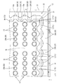
- FIG. 9 is an enlarged schematic view of the vicinity of the boundary line L between the seat inclined portion 32 and the seat bottom portion 31 on the front side surface of the chassis light reflecting sheet 22. Note that. 9, the vicinity of the boundary line L2 (L) between the second seat inclined portion 32B and the seat bottom portion 31 is enlarged.
- the upper side in FIG. 9 corresponds to the inside of the chassis 14 and the lower side corresponds to the outside of the chassis 14, respectively. Yes.
- the boundary portion F2 is a region along the boundary line L (L2) and a region including the boundary line L (L2) on the front side surface of the chassis light reflection sheet 22.
- a region having a constant width W2 with the boundary line L (L2) as the center is illustrated as the boundary portion F2.
- the separation side adjacent portions F1 and F3 are regions adjacent to the side farther than the boundary line L (upper and lower sides in FIG. 9) with respect to the boundary portion F2.
- a region having a certain width W1 disposed on the upper side of FIG. 9 (inside the chassis light reflection sheet 22) with respect to the boundary portion F2 than the boundary line L is defined as the separated adjacent portion F1.
- a region having a certain width W3 disposed on the lower side of FIG. 9 (outside of the chassis light reflection sheet 22) is defined as a separated adjacent portion F3.
- the boundary portion F2 and the separated adjacent portions F1 and F3 are regions extending along the boundary line L, respectively, and have a substantially rectangular wave shape in plan view corresponding to the shape of the boundary line L in the present embodiment.
- FIG. 9 is an enlarged view of a part of the line segment constituting the rectangular wave in the boundary line L having the rectangular wave shape.
- the separation-side adjacent portions F1 and F3 are arranged so as to sandwich the boundary portion F2 from both sides in the direction intersecting the direction along the boundary line L, respectively.
- boundary portion F2 and the separated adjacent portions F1 and F3 do not necessarily have a shape (rectangular wave shape in the present embodiment) that matches the shape of the boundary line L, and the extending direction of the boundary line L (FIG. 9). Then, it may be a rectangular area extending in the left-right direction (an area along a part of the boundary line L). Further, the widths W1 to W3 of the boundary portion F2 and the separated adjacent portions F1 and F3 can be set as appropriate.
- the light reflectance of the boundary portion F2 is set higher than the light reflectance of the separated adjacent portions F1 and F3.
- the dots 35 (35A or 35B) constituting the light reflecting portion 34 have, for example, a circular shape in plan view, and the light reflectance is set lower than the light reflectance of the chassis light reflecting sheet 22.
- Each dot 35 is formed, for example, by printing a white paste on the surface of the chassis light reflection sheet 22.
- the printing means silk printing, ink jet printing, screen printing and the like are suitable.
- the shape of the dots 35 may be a shape other than the circular shape in plan view.
- the light reflecting portion 34 lower than the light reflectance of the chassis light reflecting sheet 22 in the separated side adjacent portions F1, F3, the light reflectance of the separated side adjacent portions F1, F3 becomes the boundary of the boundary portion F2.
- a configuration lower than the light reflectivity that is, the light reflectivity of the chassis light reflection sheet 22 itself
- each dot 35 constituting the light reflecting portion 34 by changing the area of each dot 35 constituting the light reflecting portion 34, the light reflectance in the separated adjacent portions F1, F3 is changed. As described above, the light reflectance of the dot 35 itself is set lower than the light reflectance of the chassis light reflection sheet 22. For this reason, if the area of each dot 35 constituting the light reflecting portion 34 is set large, the light reflectance in the formation region of the light reflecting portion 34 is lower than the light reflectance of the chassis light reflecting sheet 22. Become.
- the present invention is not limited to this configuration. For example, it is good also as a structure which forms the 3 or more types of dot 35 from which an area becomes large in steps as it leaves
- the means for changing the area of each dot 35 of the light reflecting portion 34 is exemplified as the light reflectance adjusting means in the separated adjacent portions F1 and F3, it is not limited to this means.
- the light reflectance may be adjusted by changing the interval between the dots 35. In this case, if the interval between the dots 35 is increased, the distribution density of the dots 35 is decreased, so that the light reflectance can be relatively increased.
- FIG. 9 shows the configuration of the light reflecting portion 34 in the vicinity of the boundary line L2 between the second sheet inclined portion 32B and the sheet bottom portion 31, but in the vicinity of the boundary line L1 between the first sheet inclined portion 32A and the sheet bottom portion 31.
- the configuration of the light reflecting portion 34 is also the same configuration (a configuration in which the light reflectance decreases as the distance from the boundary line L increases).
- FIG. 7 is a view showing the emitted light (one-dot chain line) from each LED 17 at the peripheral edge of the sheet bottom 31.
- the boundary line L between the sheet bottom portion 31 and the sheet inclined portion 32 in the chassis light reflecting sheet 22 is far from each LED 17 as compared with the central portion of the chassis 14. Light emitted from the LED 17 is difficult to reach. That is, the amount of light that reaches is relatively small.
- the emission intensity of the LED 17 is remarkably high in the direction along the optical axis E1 (in FIG. 7, the emitted light along the optical axis is indicated by the arrow E1), and the inclination angle with respect to the optical axis E1. As it grows, it drops sharply. For this reason, the light reaching the boundary line L where the inclination angle from the optical axis E1 is large (approximately 90 degrees) with respect to the leading end side of the sheet inclined portion 32 having a relatively small inclination angle with respect to the optical axis E1. The amount is relatively small.
- seat inclination part 32 is shown by the arrow line E2 of FIG.
- the boundary portion F ⁇ b> 2 near the boundary line L between the sheet bottom portion 31 and the sheet inclined portion 32 has a relatively small amount of light reaching the periphery. It becomes a place.
- the boundary portion F2 has a small amount of reflected light from the chassis light reflection sheet 22.
- it is likely to be a dark part as compared with the surrounding parts (that is, the separated adjacent parts F1 and F3), and there is a risk of uneven brightness.
- the light reflectivity of the boundary portion F2 is set to be higher than the light reflectivities of the separated adjacent portions F1 and F3. If the light reflectance is set high, the amount of reflected light increases and the brightness increases. With such a configuration, the luminance of the boundary portion F2, which is a portion where the emitted light from the LED 17 is relatively difficult to reach (a portion where the amount of light reaching the portion is small), is the luminance of the adjacent adjacent side portions F1, F3. As compared with the above, it is possible to suppress the lowering, and it is possible to suppress the boundary portion F2 from becoming a dark portion.
- the surface on the LED 17 side of the chassis light reflection sheet 22 is set such that the light reflectance decreases as the distance from the boundary line L increases.
- the light reflecting portion 34 set with a light reflectance lower than the light reflectance of the chassis light reflecting sheet 22 is formed in the separated adjacent portions F1 and F3.
- the light reflectance of the boundary portion F2 can be made higher than the light reflectance of the separated adjacent portions F1 and F3.
- the chassis light reflection sheet 22 When the light reflectance of the boundary portion F2 is made higher than the light reflectance of the separated adjacent portions F1 and F3, for example, on the chassis light reflection sheet 22 having a constant light reflectance, the light reflectance is higher than the light reflectance.
- a configuration in which a high light reflecting portion is formed in the boundary portion F2 is also conceivable.
- the chassis light reflection sheet 22 is set with a high light reflectance in order to increase the light use efficiency. For this reason, it is difficult to set only the light reflectance of the boundary portion F2 higher (than the separated adjacent portions F1 and F3) on the chassis light reflection sheet 22 that is originally set to have a high light reflectance. is there.
- the light reflecting portion 34 by forming the light reflecting portion 34 having a light reflectance lower than the light reflectance of the chassis light reflecting sheet 22 in the separated adjacent portions F1, F3, the separated adjacent portions F1, F3. It was set as the structure which reduces the light reflectivity of F3. Thereby, the structure which makes the light reflectivity of the boundary part F2 high can be easily implement
- the light reflecting portion 34 is configured by a dot pattern. If the light reflecting portion 34 is configured by a dot pattern, the light reflectance of the light reflecting portion 34 can be easily set by setting the mode (area, arrangement interval, etc.) of each dot 35.
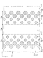
- the region (boundary portion F2) along the boundary line L between the seat bottom portion 31 and the seat inclined portion 32 tends to be a dark portion.
- the dark part D2 (the region illustrated by the one-dot chain line in FIG. 10) is also the boundary line.
- a straight line is formed corresponding to the shape of L3.
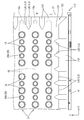
- the boundary line L has a rectangular wave shape (non-linear shape) in plan view as in the present embodiment, even if the boundary part F2 becomes a dark part D1 (a region illustrated by a one-dot chain line in FIG. 8),
- the dark portion D1 is non-linear in plan view. If the dark part D1 is non-linear, the boundary between the dark part D1 and its peripheral part is blurred compared to the case where the dark part D1 is linear, so that it is difficult to be recognized as luminance unevenness.
- the configuration in which the light reflectivity between the boundary portion F2 and the separated adjacent portions F1 and F3 described above is changed, and the configuration in which the boundary line L is non-linear.
- the boundary line L has a rectangular wave shape
- the shape of the boundary line L can be easily formed as compared with other non-linear shapes (for example, a sinusoidal curve).
- the boundary line L is to be formed as a curve
- the inclined surface of the seat inclined portion 32 needs to be curved, and there is a concern that uneven brightness may occur.
- the rectangular wave-like boundary line L as in the present embodiment allows the surface of the sheet inclined portion 32 to be configured with only a flat surface, so there is no concern that luminance unevenness will occur due to the above-described causes.
- the sheet bottom portion may have a substantially rectangular shape in a plan view, and the sheet inclined portion may extend from four sides around the sheet bottom portion.
- an LED 17 (light emitting diode) is used as the light source. Power consumption can be suppressed by using the LED 17.
- a diffusion lens 19 is provided which covers the LED 17 and can diffuse the light from the LED 17. With such a configuration, the light from the LED 17 is diffused by the diffusion lens 19. Thereby, it is possible to make the luminance uniform while increasing the arrangement interval between the LEDs (that is, while reducing the number of LEDs).
- the boundary line L3 between the bottom 131 and the inclined portion 132 in the chassis reflection sheet 122 is different from that of the first embodiment.
- the boundary line L3 includes a linear portion LA3 that forms a straight line, and a mountain-shaped portion LB3 that is formed by partially projecting the inclined portion 132 to the inside of the chassis 14.
- the bottom portion 131 and the inclined portion 132 are composed of separate members. If the bottom portion 131 and the inclined portion 132 are formed of separate members, a non-linear shape as compared with a case where the bottom portion 131 and the inclined portion 132 are formed of an integral member (for example, when the chassis reflection sheet 122 is formed by bending). It is easy to form the chassis reflection sheet 122 having the boundary line.
- the boundary portion F2 and the separated adjacent portions F1 and F3 are not limited to the regions exemplified in the above embodiment.
- the boundary portion F2 may be a region along the boundary line L between the sheet bottom portion 31 and the sheet inclined portion 32 and a region including the boundary line L on the surface on the LED 17 side of the chassis light reflection sheet 22, and the range ( The area, shape, etc.) can be set as appropriate.
- the separation-side adjacent portions F1 and F3 may be regions adjacent to the side farther from the boundary line L with respect to the boundary portion F2, and the range (area, shape, etc.) can be appropriately set.
- the configuration including the configuration for changing the light reflectance between the boundary portion F2 and the separated adjacent portions F1 and F3 and the configuration for making the boundary line L non-linear are exemplified.
- the present invention is not limited to this.
- the configuration for changing the light reflectance between the boundary portion F2 and the separated adjacent portions F1 and F3 can be applied to a configuration in which the boundary line L (L3) is linear (see FIG. 10), for example.
- the light reflectance of the boundary portion F2 is Although it was set as the structure made higher than the light reflectivity of the separation side adjacent part F1, F3, it is not limited to this.
- the light reflectance of the boundary portion F2 is changed to the light of the separated adjacent portions F1 and F3. It is good also as a structure made higher than a reflectance.
- the light reflecting portion 34 formed in the separated adjacent portions F1 and F3 is exemplified by the dot pattern, but is not limited thereto.
- the light reflecting portion 34 may be formed by making the portions corresponding to the separation-side adjacent portions F1 and F3 as separate members having a light reflectance lower than that of the chassis light reflecting sheet 22.
- the light reflectance decreases with increasing distance from the boundary line L on the surface of the chassis light reflection sheet 22 on the LED 17 side.
- the configuration is not limited to this.
- the light reflectivity of the boundary portion F2 only needs to be higher than the light reflectivity of the separated adjacent portions F1 and F3.
- the structure by which the light reflectivity of the boundary part F2 was set higher than any one of the remote side adjacent parts F1 and F3 may be sufficient.
- the boundary line (L or L3) between the bottom portion and the inclined portion in the chassis reflection sheet is a rectangular wave shape or a non-linear shape including the mountain-shaped portion LB3.
- the boundary line is a non-linear shape, it may be a non-linear shape other than the above.
- the LED 17 is exemplified as the light source, but the present invention is not limited to this, and a light source other than the LED can be applied.
- a cathode tube may be used as the light source.
- the LED substrate 18 has a configuration in which the long side direction is arranged along the X-axis direction, but is not limited thereto.
- the long side direction of the LED substrate 18 may be arranged along the Y-axis direction.
- the TFT is used as the switching element of the liquid crystal display device.
- the present invention can also be applied to a liquid crystal display device using a switching element other than TFT (for example, a thin film diode (TFD)), and color display.
- a switching element other than TFT for example, a thin film diode (TFD)
- color display for example, a liquid crystal display device.
- the present invention can be applied to a liquid crystal display device that displays black and white.
- the liquid crystal display device using the liquid crystal panel as the display panel has been exemplified.
- the present invention can also be applied to display devices using other types of display panels.
- the television receiver provided with the tuner is exemplified, but the present invention can be applied to a display device not provided with the tuner.
- SYMBOLS 10 Liquid crystal display device (display device), 11 ... Liquid crystal panel (display panel), 12, 112 ... Backlight device (illumination device), 14 ... Chassis, 14a ... Bottom plate (bottom plate of chassis), 17 ... LED (light source) , 19 ... Diffuse lens, 22 ... Light reflecting sheet for chassis (light reflecting sheet), 31 ... Sheet bottom, 32 ... Sheet inclined part, 34 ... Light reflecting part, F1, F3 ... Separated side part, F2 ... Border part, L, L1, L2, L3 ... boundary line, TV ... television receiver
Landscapes
- Physics & Mathematics (AREA)
- Nonlinear Science (AREA)
- Chemical & Material Sciences (AREA)
- Crystallography & Structural Chemistry (AREA)
- General Physics & Mathematics (AREA)
- Mathematical Physics (AREA)
- Optics & Photonics (AREA)
- Engineering & Computer Science (AREA)
- Theoretical Computer Science (AREA)
- Planar Illumination Modules (AREA)
- Transforming Electric Information Into Light Information (AREA)
Abstract
Description
上記したバックライト装置に敷設される光反射シートは、シャーシの底板に沿って配されるシート底部と、シート底部の周縁部から延び、シート底部に対して液晶パネル側へ傾斜するシート傾斜部とから構成されている。より具体的には、シート傾斜部は、シャーシの外側へ向かうにつれて、液晶パネル側へ近づく形で傾斜している。このシート傾斜部によって、反射した光を内側(液晶表示装置の中心側)に指向させることが可能となっている。
第1の理由は、境界線付近はシート底部の周縁端部に相当するから、光源からの距離がシート底部の中央側と比較して遠くなるためである。この結果、境界線付近には、シート底部の中央側と比較して、到達する光の量が相対的に少なくなる。
本発明は、光源と、前記光源が収容されるシャーシと、前記シャーシの内面側に配され、前記光源からの光を反射可能な光反射シートと、を備え、前記光源は、前記シャーシの底板に配され、前記光反射シートは、前記底板の表面に沿って延在するシート底部と、前記シート底部の周縁から延びるシート傾斜部と、を有し、前記シート傾斜部は、前記シート底部に対して、当該照明装置の光出射側に傾斜しており、前記光反射シートにおける前記光源側の面において、前記シート底部と前記シート傾斜部との境界線に沿った領域であって当該境界線を含む境界部の光反射率が、前記境界部に対して前記境界線よりも離れる側に隣接する離側隣接部の光反射率より高く設定されていることに特徴を有する。
本発明によれば、輝度ムラを抑制可能な照明装置と、このような照明装置を備えた表示装置、及びテレビ受信装置を提供することが可能となる。
本発明の実施形態1を図1ないし図10によって説明する。本実施形態では、液晶表示装置10について例示する。なお、各図面の一部にはX軸、Y軸及びZ軸が描かれており、各軸方向が各図面で共通した方向となるように描かれている。また、図4及び図5に示す上側を表側とし、同図下側を裏側とする。
本発明の実施形態2を図11によって説明する。実施形態1と同一部分には、同一符号を付して重複する説明を省略する。本実施形態のバックライト装置112において、シャーシ用反射シート122における底部131と傾斜部132との境界線L3の形状が実施形態1と相違する。境界線L3は、真っ直ぐな線状をなす線状部LA3と、傾斜部132を部分的にシャーシ14の内側へ突き出すことで形成された山型部LB3とから構成され、線状部LA3と山型部LB3とを交互に配することで、全体として非直線状をなしている。このように境界線L3を非直線状としたことによる作用及び効果は、上記実施形態1と同じであるため、説明を省略する。
本発明は上記記述及び図面によって説明した実施形態に限定されるものではなく、例えば次のような実施形態も本発明の技術的範囲に含まれる。
Claims (13)
- 光源と、
前記光源が収容されるシャーシと、
前記シャーシの内面側に配され、前記光源からの光を反射可能な光反射シートと、を備え、
前記光源は、前記シャーシの底板に配され、
前記光反射シートは、前記底板の表面に沿って延在するシート底部と、前記シート底部の周縁から延びるシート傾斜部と、を有し、
前記シート傾斜部は、前記シート底部に対して、当該照明装置の光出射側に傾斜しており、
前記光反射シートにおける前記光源側の面において、前記シート底部と前記シート傾斜部との境界線に沿った領域であって当該境界線を含む境界部の光反射率が、前記境界部に対して前記境界線よりも離れる側に隣接する離側隣接部の光反射率より高く設定されていることを特徴とする照明装置。 - 前記光反射シートにおける前記光源側の面において、前記境界線から離れるにつれて、光反射率が低くなるように設定されていることを特徴とする請求項1に記載の照明装置。
- 前記離側隣接部には、前記光反射シートの光反射率より低い光反射率で設定された光反射部が形成されていることを特徴とする請求項1又は請求項2に記載の照明装置。
- 前記光反射部はドットパターンによって構成されることを特徴とする請求項3に記載の照明装置。
- 前記シート底部と前記シート傾斜部との境界線は、平面視において、非直線状をなすことを特徴とする請求項1から請求項4のいずれか1項に記載の照明装置。
- 前記シート底部と前記シート傾斜部との境界線は、平面視において、矩形波状をなすこと特徴とする請求項5に記載の照明装置。
- 前記シート底部は、平面視において略矩形状をなし、前記シート傾斜部は、前記シート底部の周囲四辺から、それぞれ延びていることを特徴とする請求項1から請求項6のいずれか1項に記載の照明装置。
- 前記光源は発光ダイオードであることを特徴とする請求項1から請求項7のいずれか1項に記載の照明装置。
- 前記光源を覆う形で配され、前記光源からの光を拡散可能な拡散レンズを備えていることを特徴とする請求項1から請求項8のいずれか1項に記載の照明装置。
- 前記光源は、前記シャーシの底板に沿う方向に複数個行列状に配列されていることを特徴とする請求項1から請求項9のいずれか1項に記載の照明装置。
- 請求項1から請求項10のいずれか1項に記載の照明装置と、
前記照明装置からの光を利用して表示を行う表示パネルと、を備えることを特徴とする表示装置。 - 前記表示パネルが液晶を用いた液晶パネルであることを特徴とする請求項11に記載の表示装置。
- 請求項11又は請求項12に記載された表示装置を備えることを特徴とするテレビ受信装置。
Priority Applications (4)
| Application Number | Priority Date | Filing Date | Title |
|---|---|---|---|
| CN201080055721.2A CN102667311B (zh) | 2009-12-15 | 2010-10-29 | 照明装置、显示装置以及电视接收装置 |
| EP10837364.8A EP2515027A4 (en) | 2009-12-15 | 2010-10-29 | LIGHTING DEVICE, DISPLAY DEVICE AND TELEVISION RECEIVER |
| JP2011546030A JP5292476B2 (ja) | 2009-12-15 | 2010-10-29 | 照明装置、表示装置、及びテレビ受信装置 |
| US13/512,030 US8833956B2 (en) | 2009-12-15 | 2010-10-29 | Lighting device, display device and television receiver |
Applications Claiming Priority (2)
| Application Number | Priority Date | Filing Date | Title |
|---|---|---|---|
| JP2009283912 | 2009-12-15 | ||
| JP2009-283912 | 2009-12-15 |
Publications (1)
| Publication Number | Publication Date |
|---|---|
| WO2011074334A1 true WO2011074334A1 (ja) | 2011-06-23 |
Family
ID=44167099
Family Applications (1)
| Application Number | Title | Priority Date | Filing Date |
|---|---|---|---|
| PCT/JP2010/069270 Ceased WO2011074334A1 (ja) | 2009-12-15 | 2010-10-29 | 照明装置、表示装置、及びテレビ受信装置 |
Country Status (5)
| Country | Link |
|---|---|
| US (1) | US8833956B2 (ja) |
| EP (1) | EP2515027A4 (ja) |
| JP (1) | JP5292476B2 (ja) |
| CN (1) | CN102667311B (ja) |
| WO (1) | WO2011074334A1 (ja) |
Cited By (12)
| Publication number | Priority date | Publication date | Assignee | Title |
|---|---|---|---|---|
| WO2013021933A1 (ja) * | 2011-08-09 | 2013-02-14 | シャープ株式会社 | 照明装置、表示装置、及びテレビ受信装置 |
| JP2013037783A (ja) * | 2011-08-03 | 2013-02-21 | Sharp Corp | 照明装置および表示装置 |
| JP2013143273A (ja) * | 2012-01-11 | 2013-07-22 | Sharp Corp | 照明装置、表示装置及びテレビ受信装置 |
| JP2013143218A (ja) * | 2012-01-10 | 2013-07-22 | Sharp Corp | 照明装置、表示装置、及びテレビ受信装置 |
| JP2014149530A (ja) * | 2013-01-31 | 2014-08-21 | Samsung Electronics Co Ltd | ディスプレイモジュール及びそれを備えたディスプレイ装置 |
| KR20160051570A (ko) * | 2014-10-31 | 2016-05-11 | 엘지전자 주식회사 | 백라이트 유닛 및 이를 포함하는 디스플레이 장치 |
| JP2016218454A (ja) * | 2016-06-23 | 2016-12-22 | 船井電機株式会社 | 表示装置 |
| WO2017033582A1 (ja) * | 2015-08-26 | 2017-03-02 | ソニー株式会社 | 発光装置、表示装置および照明装置 |
| US9897850B2 (en) | 2012-12-26 | 2018-02-20 | Funai Electric Co., Ltd. | Display apparatus |
| WO2022250250A1 (en) * | 2021-05-24 | 2022-12-01 | Lg Electronics Inc. | Display device |
| US11566776B2 (en) | 2014-10-31 | 2023-01-31 | Lg Electronics Inc. | Display device having reflecting sheet with plurality of dot areas reducing reflectivity of the reflecting sheet |
| US12000582B2 (en) | 2014-10-31 | 2024-06-04 | Lg Electronics Inc. | Display device having reflecting sheet with plurality of dot areas reducing reflectivity of the reflecting sheet |
Families Citing this family (12)
| Publication number | Priority date | Publication date | Assignee | Title |
|---|---|---|---|---|
| EP3023835A1 (en) * | 2010-04-21 | 2016-05-25 | LG Electronics, Inc. | Display apparatus |
| KR101664422B1 (ko) | 2013-01-23 | 2016-10-10 | 엘지전자 주식회사 | 평면 조명 장치 |
| JP6146032B2 (ja) | 2013-02-05 | 2017-06-14 | 船井電機株式会社 | 表示装置 |
| KR20150068120A (ko) * | 2013-12-11 | 2015-06-19 | 삼성디스플레이 주식회사 | 백라이트 어셈블리 및 이를 포함하는 표시 장치 |
| US9785007B2 (en) * | 2014-04-09 | 2017-10-10 | Apple Inc. | Display with localized backlight dimming |
| TWI574085B (zh) * | 2014-09-11 | 2017-03-11 | 友達光電股份有限公司 | 具光均勻化設計之背光模組 |
| WO2016068592A1 (en) | 2014-10-31 | 2016-05-06 | Lg Electronics Inc. | Backlight unit and display device having backlight unit |
| EP3015912B1 (en) | 2014-10-31 | 2017-12-06 | LG Electronics Inc. | Backlight unit and display device including backlight unit |
| KR20160141983A (ko) * | 2015-06-02 | 2016-12-12 | 엘지전자 주식회사 | 디스플레이 장치 |
| KR102473397B1 (ko) * | 2016-01-28 | 2022-12-06 | 엘지전자 주식회사 | 백라이트 유닛 및 이를 포함하는 디스플레이 장치 |
| KR20170091334A (ko) * | 2016-02-01 | 2017-08-09 | 엘지전자 주식회사 | 백라이트 유닛 및 이를 포함하는 디스플레이 장치 |
| CN113841001B (zh) * | 2019-05-27 | 2024-04-12 | 三菱电机株式会社 | 照明装置 |
Citations (6)
| Publication number | Priority date | Publication date | Assignee | Title |
|---|---|---|---|---|
| WO2004031647A1 (ja) * | 2002-09-30 | 2004-04-15 | Sharp Kabushiki Kaisha | バックライトユニット及びバックライトユニットを用いた液晶表示装置 |
| JP2006146126A (ja) | 2004-11-24 | 2006-06-08 | Samsung Electronics Co Ltd | バックライトアセンブリ及びこれを有する液晶表示装置 |
| JP2007080702A (ja) * | 2005-09-15 | 2007-03-29 | Nec Lcd Technologies Ltd | バックライトユニット |
| JP2007234639A (ja) * | 2006-02-27 | 2007-09-13 | Kyocera Corp | 発光装置および照明装置 |
| JP2008300277A (ja) * | 2007-06-01 | 2008-12-11 | Hitachi Ltd | バックライトユニット |
| JP2009266625A (ja) * | 2008-04-25 | 2009-11-12 | Epson Imaging Devices Corp | 照明装置、液晶表示装置及び電子機器 |
Family Cites Families (4)
| Publication number | Priority date | Publication date | Assignee | Title |
|---|---|---|---|---|
| KR100640987B1 (ko) * | 2000-10-14 | 2006-11-02 | 엘지.필립스 엘시디 주식회사 | 액정표시장치의 직하형 백라이트 어셈블리 |
| US20100296270A1 (en) * | 2008-01-25 | 2010-11-25 | Showa Denko K.K. | Display device and light emitting device |
| RU2463517C2 (ru) * | 2008-03-05 | 2012-10-10 | Шарп Кабусики Кайся | Устройство освещения, дисплейное устройство и телевизионный приемник |
| JPWO2010146892A1 (ja) * | 2009-06-15 | 2012-12-06 | シャープ株式会社 | 照明装置、表示装置、及びテレビジョン受像器 |
-
2010
- 2010-10-29 EP EP10837364.8A patent/EP2515027A4/en not_active Withdrawn
- 2010-10-29 WO PCT/JP2010/069270 patent/WO2011074334A1/ja not_active Ceased
- 2010-10-29 US US13/512,030 patent/US8833956B2/en not_active Expired - Fee Related
- 2010-10-29 CN CN201080055721.2A patent/CN102667311B/zh not_active Expired - Fee Related
- 2010-10-29 JP JP2011546030A patent/JP5292476B2/ja not_active Expired - Fee Related
Patent Citations (6)
| Publication number | Priority date | Publication date | Assignee | Title |
|---|---|---|---|---|
| WO2004031647A1 (ja) * | 2002-09-30 | 2004-04-15 | Sharp Kabushiki Kaisha | バックライトユニット及びバックライトユニットを用いた液晶表示装置 |
| JP2006146126A (ja) | 2004-11-24 | 2006-06-08 | Samsung Electronics Co Ltd | バックライトアセンブリ及びこれを有する液晶表示装置 |
| JP2007080702A (ja) * | 2005-09-15 | 2007-03-29 | Nec Lcd Technologies Ltd | バックライトユニット |
| JP2007234639A (ja) * | 2006-02-27 | 2007-09-13 | Kyocera Corp | 発光装置および照明装置 |
| JP2008300277A (ja) * | 2007-06-01 | 2008-12-11 | Hitachi Ltd | バックライトユニット |
| JP2009266625A (ja) * | 2008-04-25 | 2009-11-12 | Epson Imaging Devices Corp | 照明装置、液晶表示装置及び電子機器 |
Non-Patent Citations (1)
| Title |
|---|
| See also references of EP2515027A4 |
Cited By (44)
| Publication number | Priority date | Publication date | Assignee | Title |
|---|---|---|---|---|
| JP2013037783A (ja) * | 2011-08-03 | 2013-02-21 | Sharp Corp | 照明装置および表示装置 |
| WO2013021933A1 (ja) * | 2011-08-09 | 2013-02-14 | シャープ株式会社 | 照明装置、表示装置、及びテレビ受信装置 |
| JP2013143218A (ja) * | 2012-01-10 | 2013-07-22 | Sharp Corp | 照明装置、表示装置、及びテレビ受信装置 |
| JP2013143273A (ja) * | 2012-01-11 | 2013-07-22 | Sharp Corp | 照明装置、表示装置及びテレビ受信装置 |
| CN110673396B (zh) * | 2012-12-26 | 2022-04-12 | 船井电机株式会社 | 显示装置 |
| CN110673396A (zh) * | 2012-12-26 | 2020-01-10 | 船井电机株式会社 | 显示装置 |
| US9897850B2 (en) | 2012-12-26 | 2018-02-20 | Funai Electric Co., Ltd. | Display apparatus |
| US11953783B2 (en) | 2013-01-31 | 2024-04-09 | Samsung Electronics Co., Ltd. | Display module and display apparatus having the same |
| US10175532B2 (en) | 2013-01-31 | 2019-01-08 | Samsung Electronics Co., Ltd. | Display module and display apparatus having the same |
| JP2014149530A (ja) * | 2013-01-31 | 2014-08-21 | Samsung Electronics Co Ltd | ディスプレイモジュール及びそれを備えたディスプレイ装置 |
| US11249347B2 (en) | 2013-01-31 | 2022-02-15 | Samsung Electronics Co., Ltd. | Display module and display apparatus having the same |
| US11619846B2 (en) | 2013-01-31 | 2023-04-04 | Samsung Electronics Co., Ltd. | Display module and display apparatus having the same |
| US10845646B2 (en) | 2013-01-31 | 2020-11-24 | Samsung Electronics Co., Ltd. | Display module and display apparatus having the same |
| US10437103B2 (en) | 2013-01-31 | 2019-10-08 | Samsung Electronics Co., Ltd. | Display module and display apparatus having the same |
| KR102309878B1 (ko) * | 2014-10-31 | 2021-10-08 | 엘지전자 주식회사 | 백라이트 유닛 및 이를 포함하는 디스플레이 장치 |
| US12000582B2 (en) | 2014-10-31 | 2024-06-04 | Lg Electronics Inc. | Display device having reflecting sheet with plurality of dot areas reducing reflectivity of the reflecting sheet |
| KR20160051570A (ko) * | 2014-10-31 | 2016-05-11 | 엘지전자 주식회사 | 백라이트 유닛 및 이를 포함하는 디스플레이 장치 |
| KR20160051567A (ko) * | 2014-10-31 | 2016-05-11 | 엘지전자 주식회사 | 백라이트 유닛 및 이를 포함하는 디스플레이 장치 |
| US12013611B2 (en) | 2014-10-31 | 2024-06-18 | Lg Electronics Inc. | Backlight unit and display device including backlight unit |
| KR102309887B1 (ko) * | 2014-10-31 | 2021-10-08 | 엘지전자 주식회사 | 백라이트 유닛 및 이를 포함하는 디스플레이 장치 |
| KR20160051569A (ko) * | 2014-10-31 | 2016-05-11 | 엘지전자 주식회사 | 백라이트 유닛 및 이를 포함하는 디스플레이 장치 |
| KR102315567B1 (ko) * | 2014-10-31 | 2021-10-21 | 엘지전자 주식회사 | 백라이트 유닛 및 이를 포함하는 디스플레이 장치 |
| KR102330349B1 (ko) * | 2014-10-31 | 2021-11-23 | 엘지전자 주식회사 | 백라이트 유닛 및 이를 포함하는 디스플레이 장치 |
| US12215856B2 (en) | 2014-10-31 | 2025-02-04 | Lg Electronics Inc. | Display device having reflecting sheet with plurality of dot areas reducing reflectivity of the reflecting sheet |
| KR20160051566A (ko) * | 2014-10-31 | 2016-05-11 | 엘지전자 주식회사 | 백라이트 유닛 및 이를 포함하는 디스플레이 장치 |
| US12493211B2 (en) | 2014-10-31 | 2025-12-09 | Lg Electronics Inc. | Backlight unit and display device including backlight unit |
| US11287691B2 (en) | 2014-10-31 | 2022-03-29 | Lg Electronics Inc. | Backlight unit and display device including backlight unit |
| KR20160051568A (ko) * | 2014-10-31 | 2016-05-11 | 엘지전자 주식회사 | 백라이트 유닛 및 이를 포함하는 디스플레이 장치 |
| KR102426038B1 (ko) * | 2014-10-31 | 2022-07-27 | 엘지전자 주식회사 | 백라이트 유닛 및 이를 포함하는 디스플레이 장치 |
| KR20220107141A (ko) * | 2014-10-31 | 2022-08-02 | 엘지전자 주식회사 | 백라이트 유닛 및 이를 포함하는 디스플레이 장치 |
| US11860474B2 (en) | 2014-10-31 | 2024-01-02 | Lg Electronics Inc. | Backlight unit and display device including backlight unit |
| US11566776B2 (en) | 2014-10-31 | 2023-01-31 | Lg Electronics Inc. | Display device having reflecting sheet with plurality of dot areas reducing reflectivity of the reflecting sheet |
| US11579487B2 (en) | 2014-10-31 | 2023-02-14 | Lg Electronics Inc. | Backlight unit and display device including backlight unit |
| KR102549805B1 (ko) | 2014-10-31 | 2023-06-29 | 엘지전자 주식회사 | 백라이트 유닛 및 이를 포함하는 디스플레이 장치 |
| WO2017033582A1 (ja) * | 2015-08-26 | 2017-03-02 | ソニー株式会社 | 発光装置、表示装置および照明装置 |
| US11578851B2 (en) | 2015-08-26 | 2023-02-14 | Saturn Licensing Llc | Light-emitting device, display apparatus and lighting apparatus |
| US11732869B2 (en) | 2015-08-26 | 2023-08-22 | Saturn Licensing Llc | Light-emitting device, display apparatus and lighting apparatus |
| US11242975B2 (en) | 2015-08-26 | 2022-02-08 | Saturn Licensing Llc | Light-emitting device, display apparatus and lighting apparatus |
| JP6991373B2 (ja) | 2015-08-26 | 2022-02-03 | ソニーグループ株式会社 | 発光装置、表示装置および照明装置 |
| JP2021073650A (ja) * | 2015-08-26 | 2021-05-13 | ソニーグループ株式会社 | 発光装置、表示装置および照明装置 |
| JPWO2017033582A1 (ja) * | 2015-08-26 | 2018-06-14 | ソニー株式会社 | 発光装置、表示装置および照明装置 |
| JP2016218454A (ja) * | 2016-06-23 | 2016-12-22 | 船井電機株式会社 | 表示装置 |
| WO2022250250A1 (en) * | 2021-05-24 | 2022-12-01 | Lg Electronics Inc. | Display device |
| US12147120B2 (en) | 2021-05-24 | 2024-11-19 | Lg Electronics Inc. | Display device with reflective sheet having color converting light patterns |
Also Published As
| Publication number | Publication date |
|---|---|
| EP2515027A1 (en) | 2012-10-24 |
| EP2515027A4 (en) | 2013-07-24 |
| JPWO2011074334A1 (ja) | 2013-04-25 |
| CN102667311A (zh) | 2012-09-12 |
| US20120287347A1 (en) | 2012-11-15 |
| US8833956B2 (en) | 2014-09-16 |
| CN102667311B (zh) | 2014-10-01 |
| JP5292476B2 (ja) | 2013-09-18 |
Similar Documents
| Publication | Publication Date | Title |
|---|---|---|
| JP5292476B2 (ja) | 照明装置、表示装置、及びテレビ受信装置 | |
| JP5298204B2 (ja) | 照明装置、表示装置、及びテレビ受信装置 | |
| JP5355714B2 (ja) | 照明装置、表示装置、及びテレビ受信装置 | |
| JP5337883B2 (ja) | 照明装置、表示装置、及びテレビ受信装置 | |
| JP5133459B2 (ja) | 照明装置、表示装置、及びテレビ受信装置 | |
| US20120262631A1 (en) | Lighting device, display device and television receiver | |
| JP5476478B2 (ja) | 照明装置、表示装置及びテレビ受信装置 | |
| US9612474B2 (en) | Backlight assembly and display device including the same | |
| WO2012014598A1 (ja) | 照明装置、表示装置及びテレビ受信装置 | |
| JPWO2011001754A1 (ja) | 照明装置、表示装置、及びテレビ受信装置 | |
| WO2011048881A1 (ja) | 照明装置、表示装置、テレビ受信装置 | |
| US8144287B2 (en) | Optical member unit, lighting device for display, display, and television receiver | |
| WO2011148694A1 (ja) | 照明装置、表示装置、及びテレビ受信装置 | |
| WO2011055635A1 (ja) | 光源ユニット用母材、照明装置、表示装置、及びテレビ受信装置 | |
| WO2011062023A1 (ja) | 照明装置、表示装置、及びテレビ受信装置 | |
| US8203668B2 (en) | Optical member unit, lighting device for display, display, and television receiver | |
| WO2013024714A1 (ja) | 照明装置、表示装置、及びテレビ受信装置 | |
| JP2013118055A (ja) | 照明装置、表示装置、及びテレビ受信装置 | |
| WO2013021933A1 (ja) | 照明装置、表示装置、及びテレビ受信装置 | |
| KR101824037B1 (ko) | 디스플레이 장치 | |
| WO2013031674A1 (ja) | 照明装置、表示装置及びテレビ受信装置 | |
| JP2013143220A (ja) | 照明装置、表示装置、及びテレビ受信装置 | |
| KR102589473B1 (ko) | 액정표시장치 및 이를 포함하는 다면 표시장치 | |
| KR101908652B1 (ko) | 백라이트 유닛 및 그를 이용한 디스플레이 장치 | |
| KR20150065009A (ko) | 백라이트 유닛 및 이를 포함하는 액정 표시 장치 |
Legal Events
| Date | Code | Title | Description |
|---|---|---|---|
| WWE | Wipo information: entry into national phase |
Ref document number: 201080055721.2 Country of ref document: CN |
|
| 121 | Ep: the epo has been informed by wipo that ep was designated in this application |
Ref document number: 10837364 Country of ref document: EP Kind code of ref document: A1 |
|
| 121 | Ep: the epo has been informed by wipo that ep was designated in this application |
Ref document number: 10837364 Country of ref document: EP Kind code of ref document: A1 |
|
| WWE | Wipo information: entry into national phase |
Ref document number: 13512030 Country of ref document: US |
|
| WWE | Wipo information: entry into national phase |
Ref document number: 2011546030 Country of ref document: JP |
|
| WWE | Wipo information: entry into national phase |
Ref document number: 2010837364 Country of ref document: EP |
|
| NENP | Non-entry into the national phase |
Ref country code: DE |