WO2011077852A1 - Iii族窒化物半導体レーザ素子、及びiii族窒化物半導体レーザ素子を作製する方法 - Google Patents
Iii族窒化物半導体レーザ素子、及びiii族窒化物半導体レーザ素子を作製する方法 Download PDFInfo
- Publication number
- WO2011077852A1 WO2011077852A1 PCT/JP2010/070214 JP2010070214W WO2011077852A1 WO 2011077852 A1 WO2011077852 A1 WO 2011077852A1 JP 2010070214 W JP2010070214 W JP 2010070214W WO 2011077852 A1 WO2011077852 A1 WO 2011077852A1
- Authority
- WO
- WIPO (PCT)
- Prior art keywords
- nitride semiconductor
- group iii
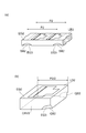
- iii nitride
- degrees
- semiconductor laser
- Prior art date
- Legal status (The legal status is an assumption and is not a legal conclusion. Google has not performed a legal analysis and makes no representation as to the accuracy of the status listed.)
- Ceased
Links
Images











Classifications
-
- H—ELECTRICITY
- H01—ELECTRIC ELEMENTS
- H01S—DEVICES USING THE PROCESS OF LIGHT AMPLIFICATION BY STIMULATED EMISSION OF RADIATION [LASER] TO AMPLIFY OR GENERATE LIGHT; DEVICES USING STIMULATED EMISSION OF ELECTROMAGNETIC RADIATION IN WAVE RANGES OTHER THAN OPTICAL
- H01S5/00—Semiconductor lasers
- H01S5/30—Structure or shape of the active region; Materials used for the active region
- H01S5/34—Structure or shape of the active region; Materials used for the active region comprising quantum well or superlattice structures, e.g. single quantum well [SQW] lasers, multiple quantum well [MQW] lasers or graded index separate confinement heterostructure [GRINSCH] lasers
- H01S5/343—Structure or shape of the active region; Materials used for the active region comprising quantum well or superlattice structures, e.g. single quantum well [SQW] lasers, multiple quantum well [MQW] lasers or graded index separate confinement heterostructure [GRINSCH] lasers in AIIIBV compounds, e.g. AlGaAs-laser, InP-based laser
-
- H—ELECTRICITY
- H01—ELECTRIC ELEMENTS
- H01S—DEVICES USING THE PROCESS OF LIGHT AMPLIFICATION BY STIMULATED EMISSION OF RADIATION [LASER] TO AMPLIFY OR GENERATE LIGHT; DEVICES USING STIMULATED EMISSION OF ELECTROMAGNETIC RADIATION IN WAVE RANGES OTHER THAN OPTICAL
- H01S5/00—Semiconductor lasers
- H01S5/30—Structure or shape of the active region; Materials used for the active region
- H01S5/34—Structure or shape of the active region; Materials used for the active region comprising quantum well or superlattice structures, e.g. single quantum well [SQW] lasers, multiple quantum well [MQW] lasers or graded index separate confinement heterostructure [GRINSCH] lasers
- H01S5/343—Structure or shape of the active region; Materials used for the active region comprising quantum well or superlattice structures, e.g. single quantum well [SQW] lasers, multiple quantum well [MQW] lasers or graded index separate confinement heterostructure [GRINSCH] lasers in AIIIBV compounds, e.g. AlGaAs-laser, InP-based laser
- H01S5/34333—Structure or shape of the active region; Materials used for the active region comprising quantum well or superlattice structures, e.g. single quantum well [SQW] lasers, multiple quantum well [MQW] lasers or graded index separate confinement heterostructure [GRINSCH] lasers in AIIIBV compounds, e.g. AlGaAs-laser, InP-based laser with a well layer based on Ga(In)N or Ga(In)P, e.g. blue laser
-
- B—PERFORMING OPERATIONS; TRANSPORTING
- B82—NANOTECHNOLOGY
- B82Y—SPECIFIC USES OR APPLICATIONS OF NANOSTRUCTURES; MEASUREMENT OR ANALYSIS OF NANOSTRUCTURES; MANUFACTURE OR TREATMENT OF NANOSTRUCTURES
- B82Y20/00—Nanooptics, e.g. quantum optics or photonic crystals
-
- H—ELECTRICITY
- H01—ELECTRIC ELEMENTS
- H01S—DEVICES USING THE PROCESS OF LIGHT AMPLIFICATION BY STIMULATED EMISSION OF RADIATION [LASER] TO AMPLIFY OR GENERATE LIGHT; DEVICES USING STIMULATED EMISSION OF ELECTROMAGNETIC RADIATION IN WAVE RANGES OTHER THAN OPTICAL
- H01S5/00—Semiconductor lasers
- H01S5/02—Structural details or components not essential to laser action
- H01S5/0201—Separation of the wafer into individual elements, e.g. by dicing, cleaving, etching or directly during growth
- H01S5/0202—Cleaving
-
- H—ELECTRICITY
- H01—ELECTRIC ELEMENTS
- H01S—DEVICES USING THE PROCESS OF LIGHT AMPLIFICATION BY STIMULATED EMISSION OF RADIATION [LASER] TO AMPLIFY OR GENERATE LIGHT; DEVICES USING STIMULATED EMISSION OF ELECTROMAGNETIC RADIATION IN WAVE RANGES OTHER THAN OPTICAL
- H01S5/00—Semiconductor lasers
- H01S5/10—Construction or shape of the optical resonator, e.g. extended or external cavity, coupled cavities, bent-guide, varying width, thickness or composition of the active region
- H01S5/1082—Construction or shape of the optical resonator, e.g. extended or external cavity, coupled cavities, bent-guide, varying width, thickness or composition of the active region with a special facet structure, e.g. structured, non planar, oblique
-
- H—ELECTRICITY
- H01—ELECTRIC ELEMENTS
- H01S—DEVICES USING THE PROCESS OF LIGHT AMPLIFICATION BY STIMULATED EMISSION OF RADIATION [LASER] TO AMPLIFY OR GENERATE LIGHT; DEVICES USING STIMULATED EMISSION OF ELECTROMAGNETIC RADIATION IN WAVE RANGES OTHER THAN OPTICAL
- H01S5/00—Semiconductor lasers
- H01S5/10—Construction or shape of the optical resonator, e.g. extended or external cavity, coupled cavities, bent-guide, varying width, thickness or composition of the active region
- H01S5/1082—Construction or shape of the optical resonator, e.g. extended or external cavity, coupled cavities, bent-guide, varying width, thickness or composition of the active region with a special facet structure, e.g. structured, non planar, oblique
- H01S5/1085—Oblique facets
-
- H—ELECTRICITY
- H01—ELECTRIC ELEMENTS
- H01S—DEVICES USING THE PROCESS OF LIGHT AMPLIFICATION BY STIMULATED EMISSION OF RADIATION [LASER] TO AMPLIFY OR GENERATE LIGHT; DEVICES USING STIMULATED EMISSION OF ELECTROMAGNETIC RADIATION IN WAVE RANGES OTHER THAN OPTICAL
- H01S5/00—Semiconductor lasers
- H01S5/10—Construction or shape of the optical resonator, e.g. extended or external cavity, coupled cavities, bent-guide, varying width, thickness or composition of the active region
- H01S5/16—Window-type lasers, i.e. with a region of non-absorbing material between the active region and the reflecting surface
-
- H—ELECTRICITY
- H01—ELECTRIC ELEMENTS
- H01S—DEVICES USING THE PROCESS OF LIGHT AMPLIFICATION BY STIMULATED EMISSION OF RADIATION [LASER] TO AMPLIFY OR GENERATE LIGHT; DEVICES USING STIMULATED EMISSION OF ELECTROMAGNETIC RADIATION IN WAVE RANGES OTHER THAN OPTICAL
- H01S5/00—Semiconductor lasers
- H01S5/30—Structure or shape of the active region; Materials used for the active region
- H01S5/32—Structure or shape of the active region; Materials used for the active region comprising PN junctions, e.g. hetero- or double- heterostructures
- H01S5/3202—Structure or shape of the active region; Materials used for the active region comprising PN junctions, e.g. hetero- or double- heterostructures grown on specifically orientated substrates, or using orientation dependent growth
- H01S5/320275—Structure or shape of the active region; Materials used for the active region comprising PN junctions, e.g. hetero- or double- heterostructures grown on specifically orientated substrates, or using orientation dependent growth semi-polar orientation
-
- H—ELECTRICITY
- H01—ELECTRIC ELEMENTS
- H01S—DEVICES USING THE PROCESS OF LIGHT AMPLIFICATION BY STIMULATED EMISSION OF RADIATION [LASER] TO AMPLIFY OR GENERATE LIGHT; DEVICES USING STIMULATED EMISSION OF ELECTROMAGNETIC RADIATION IN WAVE RANGES OTHER THAN OPTICAL
- H01S2301/00—Functional characteristics
- H01S2301/14—Semiconductor lasers with special structural design for lasing in a specific polarisation mode
-
- H—ELECTRICITY
- H01—ELECTRIC ELEMENTS
- H01S—DEVICES USING THE PROCESS OF LIGHT AMPLIFICATION BY STIMULATED EMISSION OF RADIATION [LASER] TO AMPLIFY OR GENERATE LIGHT; DEVICES USING STIMULATED EMISSION OF ELECTROMAGNETIC RADIATION IN WAVE RANGES OTHER THAN OPTICAL
- H01S5/00—Semiconductor lasers
- H01S5/0014—Measuring characteristics or properties thereof
-
- H—ELECTRICITY
- H01—ELECTRIC ELEMENTS
- H01S—DEVICES USING THE PROCESS OF LIGHT AMPLIFICATION BY STIMULATED EMISSION OF RADIATION [LASER] TO AMPLIFY OR GENERATE LIGHT; DEVICES USING STIMULATED EMISSION OF ELECTROMAGNETIC RADIATION IN WAVE RANGES OTHER THAN OPTICAL
- H01S5/00—Semiconductor lasers
- H01S5/02—Structural details or components not essential to laser action
- H01S5/028—Coatings ; Treatment of the laser facets, e.g. etching, passivation layers or reflecting layers
-
- H—ELECTRICITY
- H01—ELECTRIC ELEMENTS
- H01S—DEVICES USING THE PROCESS OF LIGHT AMPLIFICATION BY STIMULATED EMISSION OF RADIATION [LASER] TO AMPLIFY OR GENERATE LIGHT; DEVICES USING STIMULATED EMISSION OF ELECTROMAGNETIC RADIATION IN WAVE RANGES OTHER THAN OPTICAL
- H01S5/00—Semiconductor lasers
- H01S5/04—Processes or apparatus for excitation, e.g. pumping, e.g. by electron beams
- H01S5/042—Electrical excitation ; Circuits therefor
- H01S5/0425—Electrodes, e.g. characterised by the structure
- H01S5/04254—Electrodes, e.g. characterised by the structure characterised by the shape
Definitions
- the present invention relates to a group III nitride semiconductor laser device and a method for manufacturing a group III nitride semiconductor laser device.
- Patent Document 1 describes a laser device. If the surface inclined by 28.1 degrees from the ⁇ 0001 ⁇ plane toward the direction equivalent to the [1-100] direction is the main surface of the substrate, the secondary cleavage surface is both the main surface and the optical resonator surface. The ⁇ 11-20 ⁇ plane is perpendicular to the surface, and the laser device has a rectangular parallelepiped shape.
- Patent Document 2 describes a nitride semiconductor device.
- the back surface of the substrate for cleavage is polished to reduce the total thickness to about 100 ⁇ m.
- a dielectric multilayer film is deposited on the cleavage plane.
- Patent Document 3 describes a nitride-based compound semiconductor element.
- the substrate used for the nitride-based compound semiconductor element is made of a nitride-based compound semiconductor having a threading dislocation density of 3 ⁇ 10 6 cm ⁇ 2 or less, and the threading dislocation density is substantially uniform in the plane.
- Patent Document 4 describes a nitride semiconductor laser element.
- a cleavage plane is formed as follows. Using a laser scriber while avoiding the protrusions formed during the etching process of the resonator surface of the n-type GaN substrate with respect to the recesses formed by the etching process so as to reach the n-type GaN substrate from the semiconductor laser element layer
- the scribe grooves are formed in a broken line shape (at intervals of about 40 ⁇ m) in a direction orthogonal to the direction in which the ridge portion extends. Then, the wafer is cleaved at the position of the scribe groove.
- the region where the scribe groove such as the convex portion is not formed is cleaved starting from the adjacent scribe groove.
- the element isolation surfaces are each formed as a cleavage plane made of the (0001) plane of the n-type GaN substrate.
- Patent Document 5 describes a light emitting element. According to the light emitting element, long wavelength light emission can be easily obtained without impairing the light emission efficiency in the light emitting layer.
- Patent Document 6 describes a nitride semiconductor element having a counter electrode structure with reduced contact resistance.
- the nitride semiconductor substrate has a first main surface and a second main surface.
- the nitride semiconductor substrate includes a region whose crystal growth surface is a (0001) plane.
- the nitride semiconductor layer is stacked on the first main surface of the nitride semiconductor substrate.
- a recessed groove is formed in the second region of the second main surface.
- a ridge-shaped stripe is formed on the first main surface of the nitride semiconductor substrate.
- a resonator is fabricated by cleavage.
- Non-Patent Document 1 describes a semiconductor laser in which a waveguide is provided in the off direction on a semipolar (10-11) plane and a mirror is formed by a reactive ion etching method.
- the band structure of a gallium nitride semiconductor there are several transitions capable of laser oscillation.
- the laser beam is guided along a plane defined by the c-axis and the m-axis.
- the threshold current can be lowered when extending the waveguide.
- the mode with the smallest transition energy difference between conduction band energy and valence band energy
- the threshold is set. The current can be lowered.
- a conventional cleavage plane such as c-plane, a-plane or m-plane cannot be used for the resonator mirror.
- the dry etching surface of the semiconductor layer has been formed using reactive ion etching (RIE) for the fabrication of the resonator mirror.
- RIE reactive ion etching
- a resonator mirror formed by the RIE method is desired to be improved in terms of perpendicularity to a laser waveguide, flatness of a dry etching surface, or ion damage.
- derivation of process conditions for obtaining a good dry etching surface at the current technical level is a heavy burden.
- an end face different from the cleavage plane can be used as a resonator mirror.
- This end face is formed by forming a scribe groove on the epitaxial face side of the thin film and pressing the back face side of the substrate.
- the inventors have studied to improve the end face using this method to a better quality as a resonator mirror.
- the present invention has been made in view of such circumstances.
- the applicant of the present application has filed a patent application (Japanese Patent Application No. 2009-144442) related to a group III nitride semiconductor laser device including a split section for an optical resonator.
- the object of the present invention is to provide high quality and low threshold current for resonator mirrors on the semipolar plane of the support substrate tilted in the direction of c-axis to m-axis of hexagonal group III nitride
- Another object of the present invention is to provide a group III nitride semiconductor laser device having a laser resonator, and to provide a method for manufacturing the group III nitride semiconductor laser device.
- a group III nitride semiconductor laser device includes: (a) a support base made of a hexagonal group III nitride semiconductor and having a semipolar main surface; and the semipolar main surface of the support base A laser structure including the semiconductor region provided; and (b) an electrode provided on the semiconductor region of the laser structure.
- the semiconductor region includes a first cladding layer made of a gallium nitride semiconductor of a first conductivity type, a second cladding layer made of a gallium nitride semiconductor of a second conductivity type, the first cladding layer, and the first cladding layer.
- the first cladding layer, the second cladding layer and the active layer are arranged along a normal axis of the semipolar main surface.
- the active layer includes a gallium nitride based semiconductor layer, and the c-axis of the hexagonal group III nitride semiconductor of the support base is the normal axis in the direction of the m axis of the hexagonal group III nitride semiconductor.
- the angle ALPHA formed by the normal axis and the c-axis of the hexagonal group III nitride semiconductor is 45 degrees or more and 80 degrees or less, or 100 degrees or more and 135 degrees or less.
- the laser structure is A laser resonator of the group III nitride semiconductor laser device, comprising first and second fractured surfaces intersecting the mn plane defined by the m axis and the normal axis of the hexagonal group III nitride semiconductor Includes the first and second fractured surfaces, the laser structure includes first and second surfaces, and the first surface is a surface opposite to the second surface, and the semiconductor region Is located between the second surface and the support base, and the first and second fractured surfaces respectively extend from an edge of the first surface to an edge of the second surface,
- the support base of the laser structure has a recess provided in a part of the edge of the first surface in the first split cross section, and the recess extends from the back surface of the support base. Is terminated from the edge of the second surface of the semiconductor region.
- the first and second fractured sections serving as laser resonators are in the mn plane defined by the m axis and the normal axis of the hexagonal group III nitride semiconductor. Since they intersect, a laser waveguide extending in the direction of the intersecting line between the mn plane and the semipolar plane can be provided. Therefore, a group III nitride semiconductor laser device having a laser resonator that enables a low threshold current can be provided.
- a recess corresponding to the scribe mark extends from the back surface of the support base, and the end of the recess is separated from the edge of the second surface (epi surface) of the semiconductor region. Therefore, good flatness is provided to the end face of the active layer exposed in the fractured surface.
- this concave portion guides the cleaving, and a large bending moment is generated in the semiconductor on the epitaxial surface side of the semiconductor stack including the active layer, and this moment distribution is considered to improve the quality of the cleaved surface. It is done.
- the thickness of the support base is preferably 400 ⁇ m or less. This group III nitride semiconductor laser device is good for obtaining a high-quality fractured surface for the laser resonator.
- the thickness of the support base is not less than 50 ⁇ m and not more than 100 ⁇ m.
- the thickness is 50 ⁇ m or more, handling becomes easy and production yield is improved. If it is 100 ⁇ m or less, it is better to obtain a high-quality fractured surface for the laser resonator.
- the recess of the laser structure can reach the semiconductor region.
- an angle formed between the normal axis and the c axis of the hexagonal group III nitride semiconductor is in a range of not less than 63 degrees and not more than 80 degrees, or not less than 100 degrees and not more than 117 degrees. Even better.
- this group III nitride semiconductor laser device in the range of 63 degrees to 80 degrees or 100 degrees to 117 degrees, there is a high possibility that the end face formed by pressing is nearly perpendicular to the substrate main surface. Become. Further, when the angle is more than 80 degrees and less than 100 degrees, the desired flatness and perpendicularity may not be obtained.
- the laser light from the active layer is polarized in the a-axis direction of the hexagonal group III nitride semiconductor.
- a band transition capable of realizing a low threshold current has polarization.
- the light in the LED mode of the group III nitride semiconductor laser device includes the polarization component I1 in the direction of the a-axis of the hexagonal group III nitride semiconductor and the hexagonal
- the polarization component I2 is included in a direction in which the c-axis of the crystal group III nitride semiconductor is projected onto the principal surface, and the polarization component I1 is larger than the polarization component I2.
- this group III nitride semiconductor laser element light having a large emission intensity in the LED mode can be laser-oscillated using the laser resonator.
- the semipolar principal surface includes ⁇ 20-21 ⁇ plane, ⁇ 10-11 ⁇ plane, ⁇ 20-2-1 ⁇ plane, and ⁇ 10-1-1]. ⁇ Any of the surfaces is good.
- the first and second flatness and perpendicularity sufficient to configure the laser resonator of the group III nitride semiconductor laser device on these typical semipolar planes.
- Two end faces can be provided.
- the semipolar principal surface includes ⁇ 20-21 ⁇ plane, ⁇ 10-11 ⁇ plane, ⁇ 20-2-1 ⁇ plane, and ⁇ 10-1-1].
- ⁇ A plane having a slight inclination in a range of ⁇ 4 degrees or more and +4 degrees or less in the m-plane direction from any semipolar plane of the plane may be the main plane.
- the flatness and perpendicularity sufficient to configure the laser resonator of the group III nitride semiconductor laser device on the slightly inclined surface from these typical semipolar planes.
- the stacking fault density of the support base is preferably 1 ⁇ 10 4 cm ⁇ 1 or less.
- the stacking fault density is 1 ⁇ 10 4 cm ⁇ 1 or less, there is a low possibility that the flatness and / or the perpendicularity of the fractured section will be disturbed due to accidental circumstances.
- the support base may be made of any one of GaN, AlGaN, AlN, InGaN, and InAlGaN.
- the first and second end faces that can be used as a resonator can be obtained.
- an AlN substrate or an AlGaN substrate the degree of polarization can be increased, and light confinement can be enhanced by a low refractive index.
- an InGaN substrate the lattice mismatch rate between the substrate and the light emitting layer can be reduced, and the crystal quality can be improved.
- the group III nitride semiconductor laser device according to the present invention may further include a dielectric multilayer film provided on at least one of the first and second fractured faces.
- an end face coat can be applied to the fracture surface.
- the reflectance can be adjusted by the end face coating.
- the active layer may include a quantum well structure provided to generate light having a wavelength of 360 nm to 600 nm.
- This group III nitride semiconductor laser device can obtain a group III nitride semiconductor laser device that effectively utilizes polarized light in the LED mode by utilizing a semipolar plane, and can obtain a low threshold current.
- the active layer includes a quantum well structure provided so as to generate light having a wavelength of 430 nm or more and 550 nm or less.
- This group III nitride semiconductor laser device can improve quantum efficiency by reducing the piezoelectric field and improving the crystal quality of the light emitting layer region by utilizing a semipolar plane, and can generate light with a wavelength of 430 nm to 550 nm. It is good.
- an end surface of the support base and an end surface of the semiconductor region appear in each of the first and second fractured surfaces, and the active layer of the semiconductor region
- the angle formed between the end face in FIG. 5 and the reference plane perpendicular to the m-axis of the support base made of the hexagonal nitride semiconductor is (ALPHA) in the first plane defined by the c-axis and m-axis of the group III nitride semiconductor. -5) An angle in the range of not less than ALPHA + 5 degrees.
- This group III nitride semiconductor laser device has an end face that satisfies the above-described perpendicularity with respect to an angle taken from one of the c-axis and the m-axis to the other.
- the angle is preferably in the range of ⁇ 5 degrees to +5 degrees in the first plane and the second plane orthogonal to the normal axis.
- This group III nitride semiconductor laser device has an end face that satisfies the above-mentioned perpendicularity with respect to an angle defined in a plane perpendicular to the normal axis of the semipolar plane.
- the electrode extends in the direction of a predetermined axis, and the first and second fractured surfaces intersect the predetermined axis.
- the laser structure has a pair of side surfaces for the group III nitride semiconductor laser device, and the recess is located at the one end of the pair of side surfaces. can do.
- the recess is a scribe mark and this recess is located at one end of the pair of side surfaces, so that the laser stripe in the laser structure is separated from the scribe line.
- the laser structure has a pair of side surfaces for the group III nitride semiconductor laser device, and the recess is located at the one end of the pair of side surfaces.
- the support base of the laser structure has another recess spaced from the recess, the other recess extending from the back surface of the support base, and the other recess being the first recess. It is provided in a part of the edge of the first surface in either one of the first and second fractured faces, and the end of the other recess is spaced from the second surface of the semiconductor region. it can.
- the first and second fractured sections for the laser stripe in the laser structure are provided. Scribe grooves can be provided in the vicinity. Hence, these split sections can provide the laser stripe with a higher quality end face for the resonator mirror.
- the split section for the laser stripe in the laser structure is defined by two scribe grooves. Therefore, this split section can provide the laser stripe with a higher quality end face for the resonator mirror.
- Another aspect of the present invention relates to a method for manufacturing a group III nitride semiconductor laser device.
- This method includes (a) a step of preparing a substrate made of a hexagonal group III nitride semiconductor and having a semipolar main surface; and (b) a semiconductor region formed on the semipolar main surface and the substrate.
- Forming a substrate product having a laser structure, an anode electrode, and a cathode electrode comprising (c) a first surface of the substrate product in the direction of the a-axis of the hexagonal group III nitride semiconductor; A step of partially scribing; and (d) separating the substrate product by pressing the substrate product against a second surface to form another substrate product and a laser bar.
- the first surface is a surface opposite to the second surface
- the semiconductor region is located between the second surface and the substrate
- the laser bar extends from the first surface to the first surface.
- the first and second end faces extending to the second face and formed by the separation, wherein the first and second end faces constitute a laser resonator of the group III nitride semiconductor laser element,
- An anode electrode and a cathode electrode are formed on the laser structure, and the semiconductor region is formed of a first cladding layer made of a first conductivity type gallium nitride semiconductor and a second conductivity type gallium nitride semiconductor.
- the active layer includes a gallium nitride based semiconductor layer, and the c-axis of the hexagonal group III nitride semiconductor of the substrate is in the direction of the m axis of the hexagonal group III nitride semiconductor with respect to the normal axis.
- the first and second end faces intersect the mn plane defined by the m-axis and the normal axis of the hexagonal group III nitride semiconductor.
- the substrate product is separated by pressing the substrate product against the second surface.
- the first and second end faces are formed on the laser bar so as to intersect the mn plane defined by the m-axis and the normal axis of the hexagonal group III nitride semiconductor.
- the first and second end faces are provided with a mirror mirror surface having sufficient flatness, perpendicularity, or ion damage sufficient to constitute a laser resonator of the group III nitride semiconductor laser element.
- the laser waveguide extends in the direction of inclination of the c-axis of the hexagonal group III nitride, and the cavity mirror end face that can provide this laser waveguide is formed without using a dry etching surface.
- the scribe groove guides the end face generation in the laser bar, and a bending moment due to the press for generating the end face is generated in the semiconductor on the epi face side of the semiconductor stack including the active layer.
- This bending moment shows a maximum in the vicinity of a surface where breakage due to pressing occurs.
- the first and second end faces are formed on the laser bar by the pressing. This large bending moment is good because it provides good flatness to the active layer end faces exposed at these end faces. Due to the separation of the substrate product, the scribe grooves are left as scribe marks on the laser bar.
- the substrate in the step of forming the substrate product, is subjected to processing such as slicing or grinding so that the thickness of the substrate is 400 ⁇ m or less, and the first surface is It can be a processed surface formed by processing. Alternatively, it can be a surface including an electrode formed on the processed surface.
- the substrate in the step of forming the substrate product, is polished so that the thickness of the substrate is not less than 50 ⁇ m and not more than 100 ⁇ m, and the first surface is formed by the polishing. It can be a polished surface. Alternatively, it can be a surface including an electrode formed on the polished surface.
- the first and second end faces having sufficient flatness, perpendicularity, or ion damage sufficient to constitute a laser resonator of the group III nitride semiconductor laser element can be formed with high yield. .
- the angle ALPHA is preferably in a range of 63 degrees to 80 degrees and 100 degrees to 117 degrees. If the angle is less than 63 degrees or more than 117 degrees, the m-plane may appear in a part of the end face formed by pressing. Further, when the angle is more than 80 degrees and less than 100 degrees, desired flatness and perpendicularity cannot be obtained.
- the semipolar principal surface is any one of ⁇ 20-21 ⁇ plane, ⁇ 10-11 ⁇ plane, ⁇ 20-2-1 ⁇ plane, and ⁇ 10-1-1 ⁇ plane. It is good to be.
- first and second end faces without flatness, perpendicularity, or ion damage sufficient to constitute a laser resonator of the group III nitride semiconductor laser element.
- the semipolar principal surface is any one of ⁇ 20-21 ⁇ plane, ⁇ 10-11 ⁇ plane, ⁇ 20-2-1 ⁇ plane, and ⁇ 10-1-1 ⁇ plane.
- a surface having a slight inclination in a range of ⁇ 4 degrees or more and +4 degrees or less in the m-plane direction from the semipolar plane may be used as the main surface.
- the first and second layers do not have sufficient flatness, perpendicularity, or ion damage that can constitute a laser resonator of the group III nitride semiconductor laser device. Can provide end face.
- the scribe is performed using a laser scriber, a scribe groove is formed by the scribe, and the length of the scribe groove is defined by the a-axis of the hexagonal group III nitride semiconductor and the scribe groove. It is shorter than the length of the intersecting line between the an plane and the first plane defined by the normal axis.
- another substrate product and a laser bar are formed by cleaving the substrate product.
- This cleaving is caused by using a scribe groove that is shorter than the cleaving line of the laser bar.
- the end face of the active layer in each of the first and second end faces is in the hexagonal direction with respect to a reference plane perpendicular to the m-axis of the support base made of the hexagonal nitride semiconductor.
- An angle in the range of (ALPHA-5) degrees or more and (ALPHA + 5) degrees or less can be formed on the plane defined by the c-axis and m-axis of the crystal group III nitride semiconductor.
- the end face having the above-described perpendicularity can be formed with respect to the angle taken from one of the c-axis and the m-axis to the other.
- the substrate may be made of any one of GaN, AlN, AlGaN, InGaN, and InAlGaN. According to this method, when using a substrate made of these gallium nitride based semiconductors, the first and second end faces usable as a resonator can be obtained.
- scribe grooves can be formed at a pitch equal to the element width of the group III nitride semiconductor laser device.
- the method may further include a step of producing a group III nitride semiconductor laser device by separating the laser bar.
- the laser structure of the group III nitride semiconductor laser device has a pair of side surfaces for the group III nitride semiconductor laser device.
- a laser bar can be manufactured using scribe grooves formed at a pitch equal to the element width. Scribe grooves arranged at a pitch equal to the element width guide the direction of progress of cleaving. The scribe groove can improve the quality of the end face of the laser stripe located between these scribe grooves.
- scribe grooves can be formed at a pitch equal to a multiple of the element width of the group III nitride semiconductor laser device.
- the method may further include a step of producing a group III nitride semiconductor laser device by separating the laser bar.
- the laser structure of the group III nitride semiconductor laser device has a pair of side surfaces for the group III nitride semiconductor laser device. According to this method, a laser bar can be manufactured using scribe grooves formed at a pitch equal to a value multiple of the element width.
- a group III nitride semiconductor laser device includes (a) a support base composed of a hexagonal group III nitride semiconductor and having a semipolar main surface and a back surface, and the semipolar main surface of the support base A laser structure including a semiconductor region provided thereon; and (b) an electrode provided on the semiconductor region of the laser structure.
- the semiconductor region includes a first conductivity type cladding layer, a second conductivity type cladding layer, and an active layer provided between the first cladding layer and the second cladding layer,
- the cladding layer of the first conductivity type, the cladding layer of the second conductivity type, and the active layer are arranged along the normal axis of the semipolar main surface, and the hexagonal group III nitride of the support base
- the c-axis of the semiconductor is inclined at an angle ALPHA with respect to the normal axis in the m-axis direction of the hexagonal group III nitride semiconductor, and the angle ALPHA is 45 degrees or more and 80 degrees or less, or 100 degrees or more.
- the laser structure includes a first surface and a second surface, the first surface is a surface opposite to the second surface, and the semiconductor region is the second surface.
- the support base of the laser structure is located between a surface and the support base.
- the first and second scribing marks provided respectively at one end and the other end of the edge of the first surface at the end of the laser structure, wherein the first and second scribing marks are Extending along a plane defined by a normal axis and the a-axis of the hexagonal III-nitride semiconductor, the first and second scribe marks extend from the back surface of the support base, and
- the end of the laser structure has a split section connecting the edges of the first and second scribe marks and the edge of the second surface of the laser structure, and the group III nitride semiconductor laser
- the laser resonator of the element includes the split section.
- this group III nitride semiconductor laser device since it intersects the mn plane defined by the m-axis and normal axis of the hexagonal group III nitride semiconductor, the intersection of the mn plane and the semipolar plane A laser waveguide can be provided that extends in the direction of the line. Therefore, a group III nitride semiconductor laser device having a laser resonator that enables a low threshold current can be provided. Further, at an angle of less than 45 degrees and greater than 135 degrees, there is a high possibility that the end surface formed by pressing is an m-plane. If the angle is more than 80 degrees and less than 100 degrees, desired flatness and perpendicularity may not be obtained.
- First and second scribe marks are provided at the end of the laser structure.
- the first and second scribe marks are arranged along the an plane defined by the a-axis and the normal axis of the hexagonal group III nitride semiconductor. Since the arrangement of the first and second scribe traces can guide the generation of the split section for the laser resonator, the split section is provided to connect the edge of the scribe trace and the edge of the second surface of the laser structure. As a result, good flatness is provided to the end face of the active layer exposed in the fractured surface.
- the scribe marks extend from the back surface of the supporting base, and a large bending moment is generated in the semiconductor on the epi-plane side of the semiconductor stack including the active layer, and this moment distribution improves the quality of the cut surface. .
- Another aspect of the present invention relates to a method for manufacturing a group III nitride semiconductor laser device.
- the method includes: (a) a laser structure including a substrate from a hexagonal group III nitride semiconductor and a semiconductor region formed on a semipolar main surface of the substrate; and an anode formed on the laser structure. Forming a substrate product having an electrode and a cathode electrode; (b) scribing a first surface of the substrate product to form an array of scribe grooves; and (c) producing the substrate. Separating the substrate product by pressing the object against the second surface to form another substrate product and a laser bar.
- the c-axis of the hexagonal group III nitride semiconductor of the substrate is inclined at a finite angle ALPHA with respect to the normal axis in the m-axis direction of the hexagonal group III nitride semiconductor.
- ALPHA is in the range of not less than 45 degrees and not more than 80 degrees or in the range of not less than 100 degrees and not more than 135 degrees
- the semiconductor region includes a first conductivity type cladding layer, a second conductivity type cladding layer, and the first cladding layer.
- an active layer provided between the first conductivity type cladding layer, the second conductivity type cladding layer, and the active layer are formed on the semipolar main surface.
- the first surface is a surface opposite to the second surface
- the semiconductor region is located between the second surface and the substrate
- the scribe groove Each of the hexagonal group III nitride semiconductor includes an a-axis and the normal axis.
- the laser bar has first and second end faces formed by the separation, and the first and second end faces are the group III nitride semiconductor laser device. This constitutes a laser resonator.
- the substrate product is separated by pressing the substrate product against the second surface.
- the first and second end faces are formed on the laser bar so as to intersect the mn plane defined by the m-axis and the normal axis of the hexagonal group III nitride semiconductor.
- the first and second end faces are provided with a mirror mirror surface having sufficient flatness, perpendicularity, or ion damage sufficient to constitute a laser resonator of the group III nitride semiconductor laser element.
- the laser waveguide extends in the direction of inclination of the c-axis of the hexagonal group III nitride, and the cavity mirror end face that can provide this laser waveguide is formed without using a dry etching surface.
- a scribe groove is formed along the an plane with respect to the depth direction and the length direction.
- the arrangement of the scribe grooves guides the end face generation in the laser bar, and a bending moment due to the pressure for generating the end face is generated in the semiconductor on the epi face side of the semiconductor stack including the active layer.
- This bending moment shows a maximum in the vicinity of a surface where breakage due to pressing occurs.
- the first and second end faces are formed on the laser bar by the pressing. This large bending moment is good because it provides good flatness to the active layer end faces exposed at these end faces. Due to the separation of the substrate product, the scribe grooves are left as scribe marks on the laser bar.
- the high quality for the resonator mirror is exhibited on the semipolar plane of the support base in which the c-axis of the hexagonal group III nitride is inclined in the m-axis direction.
- a group III nitride semiconductor laser device having a laser resonator that enables a threshold current is provided, and according to the present invention, a method for manufacturing the group III nitride semiconductor laser device is provided.
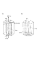
- FIG. 1 is a drawing schematically showing a structure of a group III nitride semiconductor laser device according to the present embodiment.
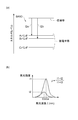
- FIG. 2 is a drawing showing a band structure in an active layer in a group III nitride semiconductor laser device.
- FIG. 3 is a drawing showing the polarization of light emission in the active layer of the group III nitride semiconductor laser device.
- FIG. 4 is a drawing showing the relationship between the end face of the group III nitride semiconductor laser device and the m-plane of the active layer.
- FIG. 5 is a process flow diagram showing the main steps of the method of manufacturing the group III nitride semiconductor laser device according to the present embodiment.
- FIG. 5 is a process flow diagram showing the main steps of the method of manufacturing the group III nitride semiconductor laser device according to the present embodiment.
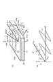
- FIG. 6 is a drawing schematically showing main steps of a method for producing a group III nitride semiconductor laser device according to the present embodiment.
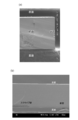
- FIG. 7 is a drawing showing a scanning electron microscope image of the end face of the resonator and a scribe mark in the split section.
- FIG. 8 is a view showing a substrate product to which a blade is applied in a supporting device for cleaving and a distribution of bending moments thereof.
- FIG. 9 is a drawing schematically showing a substrate product that is cleaved in the support device.
- FIG. 10 is a drawing showing an example of the relationship between the pitch of the scribe grooves and the scribe marks in the semiconductor laser.
- FIG. 11 is a drawing showing another example of the relationship between the pitch of the scribe grooves and the scribe marks in the semiconductor laser.
- FIG. 12 is a drawing showing still another example of the relationship between the pitch of the scribe grooves and the scribe marks in the semiconductor laser.
- FIG. 13 is a drawing showing the structure of the laser diode shown in Example 1.
- FIG. 14 is a drawing showing the ⁇ 20-21 ⁇ plane in the crystal lattice and the a-plane end face for the resonator.
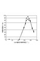
- FIG. 15 is a diagram showing the relationship between the obtained degree of polarization ⁇ and the threshold current density.
- FIG. 16 is a drawing showing the relationship between the inclination angle of the c-axis in the m-axis direction of the GaN substrate and the oscillation yield.
- FIG. 16 is a drawing showing the relationship between the inclination angle of the c-axis in the m-axis direction of the GaN substrate and the oscillation yield.
- FIG. 17 is a diagram showing the relationship between stacking fault density and oscillation yield.
- FIG. 18 is a diagram showing the relationship between the substrate thickness and the oscillation yield.
- FIG. 19 is a view showing an angle formed by the (20-21) plane and another plane orientation (index).
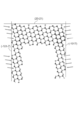
- FIG. 20 is a drawing showing atomic arrangements in the (20-21) plane, the ( ⁇ 101-6) plane, and the ( ⁇ 1016) plane.
- FIG. 21 is a drawing showing atomic arrangements in the (20-21) plane, the ( ⁇ 101-7) plane, and the ( ⁇ 1017) plane.
- FIG. 22 is a drawing showing atomic arrangements in the (20-21) plane, the ( ⁇ 101-8) plane, and the ( ⁇ 1018) plane.
- FIG. 1 is a drawing schematically showing the structure of a group III nitride semiconductor laser device according to the present embodiment.
- group III nitride semiconductor laser device 11 has a gain guide type structure, the embodiment of the present invention is not limited to the gain guide type structure.
- the group III nitride semiconductor laser device 11 includes a laser structure 13 and an electrode 15.
- the laser structure 13 includes a support base 17 and a semiconductor region 19.
- the support base 17 is made of a hexagonal group III nitride semiconductor and has a semipolar main surface 17a and a back surface 17b.
- the semiconductor region 19 is provided on the semipolar main surface 17 a of the support base 17.
- the electrode 15 is provided on the semiconductor region 19 of the laser structure 13.
- the semiconductor region 19 includes a first cladding layer 21, a second cladding layer 23, and an active layer 25.
- the first cladding layer 21 is made of a first conductivity type gallium nitride semiconductor, and is made of, for example, n-type AlGaN, n-type InAlGaN, or the like.
- the second cladding layer 23 is made of a second conductivity type gallium nitride based semiconductor, for example, p-type AlGaN, p-type InAlGaN, or the like.
- the active layer 25 is provided between the first cladding layer 21 and the second cladding layer 23.
- the active layer 25 includes a gallium nitride based semiconductor layer, and this gallium nitride based semiconductor layer is, for example, a well layer 25a.
- the active layer 25 includes barrier layers 25b made of a gallium nitride semiconductor, and the well layers 25a and the barrier layers 25b are alternately arranged.
- the well layer 25a is made of, for example, InGaN
- the barrier layer 25b is made of, for example, GaN, InGaN, or the like.
- the active layer 25 can include a quantum well structure provided to generate light having a wavelength of 360 nm to 600 nm. Use of a semipolar surface is good for generation of light having a wavelength of 430 nm or more and 550 nm or less.
- the first cladding layer 21, the second cladding layer 23, and the active layer 25 are arranged along the normal axis NX of the semipolar principal surface 17a.
- the laser structure 13 includes the first fractured surface 27 and the first section 27 intersecting the mn plane defined by the m axis and the normal axis NX of the hexagonal group III nitride semiconductor. 2 split sections 29 are included.
- FIG. 1 an orthogonal coordinate system S and a crystal coordinate system CR are drawn.
- the normal axis NX is directed in the direction of the Z axis of the orthogonal coordinate system S.
- the semipolar principal surface 17a extends in parallel to a predetermined plane defined by the X axis and the Y axis of the orthogonal coordinate system S.
- FIG. 1 also shows a representative c-plane Sc.
- the c-axis of the hexagonal group III nitride semiconductor of the support base 17 is inclined at a finite angle ALPHA with respect to the normal axis NX in the m-axis direction of the hexagonal group III nitride semiconductor.
- the group III nitride semiconductor laser device 11 further includes an insulating film 31.
- the insulating film 31 covers the surface 19 a of the semiconductor region 19 of the laser structure 13, and the semiconductor region 19 is located between the insulating film 31 and the support base 17.
- the support base 17 is made of a hexagonal group III nitride semiconductor.
- the insulating film 31 has an opening 31a.
- the opening 31a extends in the direction of the intersection line LIX between the surface 19a of the semiconductor region 19 and the mn plane, and has, for example, a stripe shape.
- the electrode 15 is in contact with the surface 19a (for example, the second conductivity type contact layer 33) of the semiconductor region 19 through the opening 31a, and extends in the direction of the intersection line LIX.
- the laser waveguide includes the first cladding layer 21, the second cladding layer 23, and the active layer 25, and extends in the direction of the intersection line LIX.
- the first fractured surface 27 and the second fractured surface 29 intersect the mn plane defined by the m-axis and the normal axis NX of the hexagonal group III nitride semiconductor.
- the laser resonator of the group III nitride semiconductor laser device 11 includes first and second fractured faces 27 and 29, and a laser waveguide is provided from one of the first fractured face 27 and the second fractured face 29 to the other. It is extended.
- the laser structure 13 includes a first surface 13a and a second surface 13b, and the first surface 13a is a surface opposite to the second surface 13b.
- the semiconductor region 10 is provided between the second surface 13 b and the support base 17.
- the first and second fractured surfaces 27 and 29 extend from the edge 13c of the first surface 13a to the edge 13d of the second surface 13b.
- the first and second fractured surfaces 27 and 29 are different from conventional cleavage planes such as c-plane, m-plane, or a-plane.
- the group III nitride semiconductor laser device 11 According to the group III nitride semiconductor laser device 11, the first and second fractured surfaces 27 and 29 constituting the laser resonator intersect with the mn plane. Therefore, it is possible to provide a laser waveguide extending in the direction of the intersecting line between the mn plane and the semipolar plane 17a. Therefore, the group III nitride semiconductor laser device 11 has a laser resonator that enables a low threshold current.
- the support base 17 of the laser structure 13 has a recess provided in one of the fractured surfaces (for example, the first fractured surface 27).
- FIG. 1 shows a recess 30 having an exemplary shape.
- the recess 30 extends from the back surface 17 b of the support base 17.
- the recess 30 is provided in a part of the edge 13c of the first surface 13a.
- the end 30a of the recess 30 is spaced from the edge 13d of the second surface 13b.
- the recess 30 corresponds to the scribe groove before cleaving, and is therefore a scribe mark.
- the scribe groove is provided on the back surface of the substrate.
- Breakage can be caused by pressing the blade toward the thin film side opposite to the back surface of the substrate.
- the end face for the optical resonator thus provided has excellent flatness and perpendicularity as a split section.
- Such a resonator mirror can provide a high oscillation yield for a semiconductor laser on a semipolar plane. Since the recess 30 is associated with a scribe groove, the scribe groove serves to guide the direction in which the cleaving proceeds in order to provide the laser structure 13 with a split section for the resonator. In addition, a scribe groove is formed on the back surface of the substrate (support base 17), and the second surface 13b of the laser structure 13 is pressed.
- the cleaving proceeds in the direction from the first surface 13a to the second surface 13b with the scribe groove as a starting point, and also proceeds in the direction intersecting this. Further, the bending moment due to the pressing force for cleaving changes in the surface layer of the second surface (epi surface) 13b, and the value of this bending moment is the scribe groove when the pressing force for cleaving is applied. It is considered that the maximum is in a plane or a line defined by the direction of arrangement. A large bending moment is considered to be one useful for forming an excellent resonator mirror.
- the recess 30 extends along the an plane defined by the a-axis and the normal axis NX of the hexagonal group III nitride semiconductor. Therefore, better flatness is provided to the active layer end face exposed in the fractured surface 27.
- the recess 30 extends from the back surface 17b of the support base 17, and the end 30a of the recess 30 is spaced from the edge 13d of the second surface (epi surface) 13b.
- the side edge 30 b of the recess 30 extends along the side surface 20 a of the group III nitride semiconductor laser device 11.
- the side edge 30b passes through the opening 31a of the insulating film 31 and the light emitting region of the active layer 25 and is spaced from a reference plane defined in the direction of the normal axis NX.
- the edge 13d of the second surface 13b extends from one end (for example, the side surface 20a) of one of the pair of side surfaces (20a, 20b) of the laser structure 13 to the other end (for example, the side surface 20b). There is no scribe mark on the edge of the epi plane.
- the edge 13c extends from one end of one of the pair of side surfaces (20a, 20b) (for example, the side surface 20a) to the side edge 30b.
- the recess 30 extends from the side surface 20b along the an plane. The recess 30 is located at one end of the side surface 20a.
- the support base 17 of the laser structure 13 can have a recess 32 corresponding to the scribe groove provided on the other split section (for example, the second split section 29).
- the recess 32 extends along the side surface 20a of the group III nitride semiconductor laser device 11, for example.
- the recessed portion 32 also includes a scribe mark as in the recessed portion 30.
- the recess 32 can also have the same shape as the recess 30, for example.
- the recess 32 also extends along the an plane like the recess 30.
- Scribe groove is useful for guiding the direction of breaking.
- the recesses 30 and 32 may reach the semiconductor region 19.
- the group III nitride semiconductor laser device 11 includes an n-side light guide layer 35 and a p-side light guide layer 37.
- the n-side light guide layer 35 includes a first portion 35a and a second portion 35b, and the n-side light guide layer 35 is made of, for example, GaN, InGaN, or the like.
- the p-side light guide layer 37 includes a first portion 37a and a second portion 37b, and the p-side light guide layer 37 is made of, for example, GaN, InGaN, or the like.
- the carrier block layer 39 is provided, for example, between the first portion 37a and the second portion 37b.
- Another electrode 41 is provided on the back surface 17b of the support base 17, and the electrode 41 covers, for example, the back surface 17b of the support base 17.
- FIG. 2 is a drawing showing a band structure in an active layer in a group III nitride semiconductor laser device.
- FIG. 3 is a drawing showing the polarization of light emission in the active layer 25 of the group III nitride semiconductor laser device 11.
- FIG. 4 is a drawing schematically showing a cross section defined by the c-axis and the m-axis. Referring to FIG. 2A, there are three possible transitions between the conduction band and the valence band in the vicinity of the ⁇ point of the band structure BAND. The A band and the B band are relatively small energy differences.
- the light emission due to the transition Ea between the conduction band and the A band is polarized in the a-axis direction, and the light emission due to the transition Eb between the conduction band and the B band is polarized in the direction projected on the principal plane.
- the threshold value of the transition Ea is smaller than the threshold value of the transition Eb.
- the light in the LED mode includes a polarization component I1 in the direction of the a-axis of the hexagonal group III nitride semiconductor and a polarization component I2 in a direction of projecting the c-axis of the hexagonal group III nitride semiconductor on the main surface,
- the polarization component I1 is larger than the polarization component I2.
- the degree of polarization ⁇ is defined by (I1 ⁇ I2) / (I1 + I2).
- dielectric multilayer films 43a and 43b provided on at least one of the first and second fractured surfaces 27 and 29, or on each of them, can be further provided.
- An end face coat can also be applied to the fracture surfaces 27 and 29. The reflectance can be adjusted by the end face coating.
- the laser light L from the active layer 25 is polarized in the direction of the a-axis of the hexagonal group III nitride semiconductor.
- the band transition capable of realizing a low threshold current has polarization.
- the first and second fractured surfaces 27 and 29 for the laser resonator are different from conventional cleavage planes such as c-plane, m-plane or a-plane.
- the first and second fractured surfaces 27 and 29 have flatness and perpendicularity as mirrors for the resonator. Therefore, using the first and second fractured surfaces 27 and 29 and the laser waveguide extending between these fractured surfaces 27 and 29, as shown in FIG.
- the end surface 17c of the support base 17 and the end surface 19c of the semiconductor region 19 appear in each of the first and second fractured surfaces 27 and 29, and the end surface 17c and the end surface 19c are It is covered with a dielectric multilayer film 43a.
- An angle BETA formed by the normal vector NA of the end face 17c of the support substrate 17 and the end face 25c of the active layer 25 and the m-axis vector MA of the active layer 25 is defined by the c-axis and m-axis of the group III nitride semiconductor.
- the component (BETA) 1 is preferably in the range of (ALPHA-5) degrees to (ALPHA + 5) degrees in the first plane S1 defined by the c-axis and m-axis of the group III nitride semiconductor. This angle range is shown in FIG. 4 as an angle formed by a representative m-plane SM and the reference plane F A.
- a representative m-plane SM is depicted from the inside to the outside of the laser structure in FIG. 4 for ease of understanding.
- the reference plane F A extends along the end face 25c of the active layer 25.
- This group III nitride semiconductor laser device 11 has an end surface that satisfies the above-described perpendicularity with respect to an angle BETA taken from one of the c-axis and the m-axis to the other.
- the component (BETA) 2 is preferably in the range of ⁇ 5 degrees or more and +5 degrees or less in the second plane S2.
- BETA 2 (BETA) 1 2 + (BETA) 2 2 .
- the end faces 27 and 29 of the group III nitride semiconductor laser device 11 satisfy the above-described perpendicularity with respect to an angle defined in a plane perpendicular to the normal axis NX of the semipolar surface 17a.
- the thickness DSUB of the support base 17 is preferably 400 ⁇ m or less. This group III nitride semiconductor laser device is good for obtaining a high-quality fractured surface for the laser resonator.
- the thickness DSUB of the support base 17 is more preferably 50 ⁇ m or more and 100 ⁇ m or less. This group III nitride semiconductor laser device 11 is better for obtaining a high-quality fractured surface for the laser resonator. Moreover, handling becomes easy and production yield can be improved.
- the angle ALPHA formed by the normal axis NX and the c-axis of the hexagonal group III nitride semiconductor is preferably 45 degrees or more, and preferably 80 degrees or less.
- the angle ALPHA is preferably 100 degrees or more and 135 degrees or less. If the angle is less than 45 degrees or more than 135 degrees, there is a high possibility that the end face formed by pressing is an m-plane. Further, when the angle is more than 80 degrees and less than 100 degrees, the desired flatness and perpendicularity may not be obtained.
- the angle ALPHA formed by the normal axis NX and the c-axis of the hexagonal group III nitride semiconductor is more preferably 63 degrees or more, and preferably 80 degrees or less.
- the angle ALPHA is preferably 100 degrees or more, and preferably 117 degrees or less. If the angle is less than 63 degrees or more than 117 degrees, the m-plane may appear in a part of the end face formed by pressing. Further, when the angle is more than 80 degrees and less than 100 degrees, the desired flatness and perpendicularity may not be obtained.
- the semipolar main surface 17a can be any one of ⁇ 20-21 ⁇ plane, ⁇ 10-11 ⁇ plane, ⁇ 20-2-1 ⁇ plane, and ⁇ 10-1-1 ⁇ plane. Further, a plane slightly inclined from these planes within a range of ⁇ 4 degrees or more and +4 degrees or less may be used as the main surface.
- the first and second end surfaces 27 and 29 having sufficient flatness and perpendicularity that can constitute the laser resonator of the group III nitride semiconductor laser device 11 can be provided.
- an end face exhibiting sufficient flatness and perpendicularity can be obtained.
- the stacking fault density of the support base 17 can be 1 ⁇ 10 4 cm ⁇ 1 or less. Since the stacking fault density is 1 ⁇ 10 4 cm ⁇ 1 or less, there is a low possibility that the flatness and / or perpendicularity of the fractured section will be disturbed due to accidental circumstances.
- the support base 17 can be made of any one of GaN, AlN, AlGaN, InGaN, and InAlGaN. When these gallium nitride semiconductor substrates are used, end faces 27 and 29 that can be used as resonators can be obtained.
- the degree of polarization can be increased, and light confinement can be enhanced by a low refractive index.
- the lattice mismatch rate between the substrate and the light emitting layer can be reduced, and the crystal quality can be improved.
- FIG. 5 is a drawing showing the main steps of a method for producing a group III nitride semiconductor laser device according to the present embodiment.
- the substrate 51 is shown.
- step S101 a substrate 51 for preparing a group III nitride semiconductor laser device is prepared.
- the c-axis (vector VC) of the hexagonal group III nitride semiconductor of the substrate 51 is inclined at a finite angle ALPHA with respect to the normal axis NX in the m-axis direction (vector VM) of the hexagonal group III nitride semiconductor. ing. Therefore, the substrate 51 has a semipolar main surface 51a made of a hexagonal group III nitride semiconductor.
- a substrate product SP is formed.
- the substrate product SP is depicted as a substantially disk-shaped member, but the shape of the substrate product SP is not limited to this.
- the laser structure 55 is formed.
- the laser structure 55 includes a semiconductor region 53 and a substrate 51.
- the semiconductor region 53 is formed on the semipolar main surface 51a.
- a first conductivity type gallium nitride based semiconductor region 57, a light emitting layer 59, and a second conductivity type gallium nitride based semiconductor region 61 are sequentially grown on the semipolar main surface 51a.
- the gallium nitride based semiconductor region 57 can include, for example, an n-type cladding layer, and the gallium nitride based semiconductor region 61 can include, for example, a p-type cladding layer.
- the light emitting layer 59 is provided between the gallium nitride based semiconductor region 57 and the gallium nitride based semiconductor region 61, and may include an active layer, a light guide layer, an electron blocking layer, and the like.
- the gallium nitride based semiconductor region 57, the light emitting layer 59, and the second conductivity type gallium nitride based semiconductor region 61 are arranged along the normal axis NX of the semipolar principal surface 51a.
- the semiconductor region 53 is covered with an insulating film 54.
- the insulating film 54 is made of, for example, silicon oxide.
- An opening 54 a of the insulating film 54 is provided.
- the opening 54a has, for example, a stripe shape.
- the anode electrode 58a and the cathode electrode 58b are formed on the laser structure 55.
- the back surface of the substrate used for crystal growth is polished to form a substrate product SP having a desired thickness DSUB.
- the anode electrode 58a is formed on the semiconductor region 53
- the cathode electrode 58b is formed on the back surface (polishing surface) 51b of the substrate 51.
- the anode electrode 58a extends in the X-axis direction
- the cathode electrode 58b covers the entire back surface 51b.
- step S105 the first surface 63a of the substrate product SP is scribed as shown in part (b) of FIG. This scribing is performed using a laser scriber 10a.
- a scribe groove 65a is formed by scribing.
- FIG. 6B five scribe grooves have already been formed, and the formation of the scribe groove 65b is being advanced using the laser beam LB.
- the length of the scribe groove 65a is shorter than the length of the intersection line AIS between the an plane and the first plane 63a defined by the a axis and the normal axis NX of the hexagonal group III nitride semiconductor.
- the laser beam LB is irradiated on a part of the AIS.
- a groove extending in a specific direction and reaching the semiconductor region is formed in the first surface 63a.
- the scribe groove 65a can be formed at one edge of the substrate product SP, for example.
- a plurality of scribe grooves arranged along the cross line AIS can be formed.
- the axis of the laser beam LB is adjusted with respect to the first surface 63a so that the laser beam LB enters the first surface 63a substantially perpendicularly. Good to do.
- the range of the axis deviation of the laser beam LB can be, for example, not less than ⁇ 5 degrees and not more than +5 degrees with respect to the normal axis of the first surface 63a.
- the scribe groove 65a is useful for guiding the direction in which the breaking proceeds.
- the scribe groove 65a has a depth (value in the Z-axis direction), a width (value in the X-axis direction), and a length (value in the Y-axis direction). It extends along the n-plane.
- the scribe groove 65 a serves to guide the direction in which the cleavage proceeds, and is formed on the back surface 51 a of the substrate (support base 17) 51.
- the second surface 63b of the laser structure 55 is pressed. The cleaving proceeds in the direction from the first surface 63a to the second surface 63b with the scribe groove 65a as a starting point, and also proceeds in the direction intersecting this.
- the bending moment due to the pressing force for cleaving is distributed on the surface layer of the second surface (epi-surface) 63b, and this bending moment distribution is maximum on the plane or line that defines the arrangement direction of the scribe grooves 65a. Therefore, it is preferable to apply a pressing force for cleaving according to this plane or line. A large bending moment is considered to be one useful for forming an excellent resonator mirror.
- step S106 the substrate product SP is separated by pressing the substrate product SP against the second surface 63b to form the substrate product SP1 and the laser bar LB1.
- the pressing is performed using a breaking device such as a blade 69.
- the blade 69 includes an edge 69a extending in one direction and at least two blade surfaces 69b and 69c defining the edge 69a.
- the substrate product SP1 is pressed on the support device 70.
- the support device 70 includes a support surface 70a and a recess 70b, and the recess 70b extends in one direction.
- the recess 70b is formed in the support surface 70a.
- the substrate product SP1 is positioned on the recess 70b on the support device 70 by aligning the direction and position of the scribe groove 65a of the substrate product SP1 with the extending direction of the recess 70b of the support device 70.
- the direction of the edge of the breaking device is aligned with the extending direction of the recess 70b, and the edge of the breaking device is pressed against the substrate product SP1 from the direction intersecting the second surface 63b.
- the intersecting direction is preferably substantially perpendicular to the second surface 63b. Thereby, the substrate product SP is separated to form the substrate product SP1 and the laser bar LB1.
- the laser bar LB1 having the first and second end faces 67a and 67b is formed, and these end faces 67a and 67b are at least perpendicular to the light emitting layer and applicable to the resonant mirror of the semiconductor laser. It has flatness.
- An array of scribe grooves is formed on the back surface 51b of the substrate 51 and the second surface 63b of the laser structure 55 is pressed so as to guide the direction in which the cleaving proceeds.
- the cleaving proceeds in the direction from the first surface 63a to the second surface 63b (for example, the Z-axis direction) starting from the scribe groove, and also proceeds in the direction intersecting this (for example, the Y-axis direction).
- scribe grooves can be formed at a pitch equal to the element width of the group III nitride semiconductor laser element. Since the scribe grooves are formed at a pitch of the element width, the cleaving guidance is performed at a distance for each element in progressing to the cleaving in the Y-axis direction. Therefore, reliable guidance can be expected with respect to the generation direction of the cleaving. Scribe grooves arranged at a pitch equal to the element width guide the direction of progress of cleaving. This arrangement can improve the quality of the end face of the laser stripe located between these scribe grooves.
- scribe grooves can be formed at a pitch equal to a value that is a multiple of the element width of the group III nitride semiconductor laser element.
- a pitch equal to twice the element width
- Scribe grooves arranged at a pitch equal to twice the element width guide the direction of cleaving. This arrangement can improve the quality of the end faces of the two laser stripes located between these scribe grooves.
- a resonator mirror having excellent flatness and perpendicularity is formed when a scribe groove and its array are formed on the back surface of the substrate along a plane defined by the a-axis and the normal axis, and when the blade is pressed against the thin film side. It can be manufactured, and it becomes possible to improve the oscillation yield of the semiconductor laser on the semipolar plane.
- the formed laser bar LB1 has first and second end surfaces 67a and 67b formed by the above separation, and each of the end surfaces 67a and 67b extends from the first surface 63a to the second surface 63b.
- the end faces 67a and 67b constitute a laser resonator of the group III nitride semiconductor laser element and intersect the XZ plane.
- This XZ plane corresponds to the mn plane defined by the m-axis and the normal axis NX of the hexagonal group III nitride semiconductor.
- the substrate product SP is pressed against the second surface 63b.
- the product SP is separated to form a new substrate product SP1 and a laser bar LB1. Therefore, the first and second end faces 67a and 67b are formed on the laser bar LB1 so as to intersect the mn plane.
- This end face formation provides sufficient flatness and perpendicularity to the extent that a laser resonator of the group III nitride semiconductor laser element can be formed on the first and second end faces 67a and 67b.
- the formed laser waveguide extends in the direction of the c-axis inclination of the hexagonal group III nitride.
- a resonator mirror end face capable of providing this laser waveguide is formed without using a dry etching surface.
- a new substrate product SP1 and a laser bar LB1 are formed by cleaving the substrate product SP1.
- separation by pressing is repeated to produce a large number of laser bars.
- This cleaving is caused by using a scribe groove 65a shorter than the breaking line BRAK of the laser bar LB1.
- step S108 a dielectric multilayer film is formed on the end faces 67a and 67b of the laser bar LB1 to form a laser bar product.
- step S109 the laser bar product is separated into individual semiconductor laser chips. A pair of side surfaces for the semiconductor laser is formed on the semiconductor laser chip.
- the group III nitride semiconductor laser device is manufactured by separating the laser bar LB1 or the laser bar product.
- the scribe groove is formed at a pitch equal to the element width of the group III nitride semiconductor laser device when the substrate product SP is scribed, the position of the scribe groove can be aligned with the separation position in the laser bar.
- the laser bar LB1 or the laser bar product is separated so that the pair of side surfaces for the semiconductor laser is aligned with the position of the scribe groove.
- the laser stripe can be separated from the pair of side surfaces for the semiconductor laser, and the position of the scribe groove (scribe mark) can be separated from the laser stripe.
- scribe grooves can be formed at a pitch equal to a value multiple of the element width of the group III nitride semiconductor laser element.
- the position of the scribe grooves can be aligned with the position of chip separation in the laser bar.
- the laser bar LB1 or the laser bar product is separated so that either one of the side surfaces for the semiconductor laser is aligned with the position of the scribe groove.
- the angle ALPHA can be in the range of 45 degrees to 80 degrees and 100 degrees to 135 degrees. If the angle is less than 45 degrees or more than 135 degrees, there is a high possibility that the end face formed by pressing is an m-plane. Further, when the angle is more than 80 degrees and less than 100 degrees, the desired flatness and perpendicularity may not be obtained.
- the angle ALPHA is preferably in the range of 63 degrees to 80 degrees and 100 degrees to 117 degrees. If the angle is less than 45 degrees or more than 135 degrees, the m-plane may appear in a part of the end face formed by pressing.
- the semipolar main surface 51a can be any one of ⁇ 20-21 ⁇ plane, ⁇ 10-11 ⁇ plane, ⁇ 20-2-1 ⁇ plane, and ⁇ 10-1-1 ⁇ plane. Further, a plane slightly inclined from these planes within a range of ⁇ 4 degrees or more and +4 degrees or less may be used as the main surface. In these typical semipolar planes, it is possible to provide an end face for the laser resonator with sufficient flatness and perpendicularity that can constitute the laser resonator of the group III nitride semiconductor laser device.
- the substrate 51 can be made of any one of GaN, AlN, AlGaN, InGaN, and InAlGaN. When these gallium nitride semiconductor substrates are used, an end face that can be used as a laser resonator can be obtained.
- the substrate 51 is preferably made of GaN.
- step S104 for forming the substrate product SP the semiconductor substrate used for crystal growth was subjected to processing such as slicing or grinding so that the substrate thickness was 400 ⁇ m or less, and the first surface 63b was formed by polishing. It can be a machined surface. With this substrate thickness, end faces 67a and 67b free from flatness, perpendicularity, or ion damage sufficient to constitute a laser resonator of the group III nitride semiconductor laser device can be formed with high yield. It is even better if the first surface 63b is a polished surface formed by polishing and the substrate thickness is 100 ⁇ m or less after being polished. In order to handle the substrate product SP relatively easily, the substrate thickness is preferably 50 ⁇ m or more.
- the angle BETA described with reference to FIG. 3 is also defined for the laser bar LB1.
- the component (BETA) 1 of the angle BETA 1 is in a first plane (surface corresponding to the first plane S1 in the description with reference to FIG. 3) defined by the c-axis and the m-axis of the group III nitride semiconductor. It is preferable that the range is not less than (ALPHA-5) degrees and not more than (ALPHA + 5) degrees.
- the end faces 67a and 67b of the laser bar LB1 satisfy the above-described perpendicularity with respect to the angle component of the angle BETA taken from one of the c-axis and the m-axis to the other.
- the component (BETA) 2 of the angle BETA is preferably in the range of ⁇ 5 degrees or more and +5 degrees or less on the second plane (the plane corresponding to the second plane S2 shown in FIG. 3).
- the end faces 67a and 67b of the laser bar LB1 satisfy the above-described perpendicularity with respect to the angle component of the angle BETA defined by the plane perpendicular to the normal axis NX of the semipolar surface 51a.
- the end faces 67a and 67b are formed by a break by pressing against a plurality of gallium nitride based semiconductor layers epitaxially grown on the semipolar surface 51a. Because of the epitaxial film on the semipolar surface 51a, the end surfaces 67a and 67b are not cleaved surfaces with a low index such as the c-plane, m-plane, or a-plane that have been used as resonator mirrors. However, in the break of the lamination of the epitaxial film on the semipolar surface 51a, the end surfaces 67a and 67b have flatness and perpendicularity applicable as resonator mirrors.
- Example 1 A semipolar plane GaN substrate was prepared as follows, and the perpendicularity of the fractured surface was observed.
- the substrate used was a ⁇ 20-21 ⁇ plane GaN substrate cut from a (0001) GaN ingot grown thick by HVPE at an angle of 75 degrees in the m-axis direction.
- the main surface of the GaN substrate was mirror-finished and the back surface was polished and finished in a satin state.
- the thickness of the substrate was 370 ⁇ m.
- a marking line was put on the back side of the satin surface perpendicular to the direction in which the c-axis was projected onto the main surface of the substrate using a diamond pen, and then pressed to cleave the substrate.
- the substrate was observed from the a-plane direction using a scanning electron microscope.
- Part (a) is a scanning electron microscope image obtained by observing the fractured surface from the a-plane direction, and the right end surface is the fractured surface. It can be seen that the split section has flatness and perpendicularity with respect to the semipolar principal surface.
- Part (b) of FIG. 7 is a scanning electron microscope image obtained by observing the surface of the fractured surface, and a scribe mark is formed on the back surface of the substrate.
- front surface indicates an epi surface
- “back surface” indicates the back surface of the substrate. The thickness of this substrate was 90 ⁇ m.
- a break in the substrate product SP1 in which the scribe groove is formed on the back surface of the substrate will be described.
- the substrate product SP1 is supported on the support surface 70a of the support device 70 for cleaving.
- the orientation of the scribe grooves 65a in the substrate product SP1 is aligned with the direction of the recess 70b.
- the scribe groove 65a has side surfaces 64a and 64b, a bottom surface 64c, and a pair of end surfaces 64d.
- the bending moment in the surface layer of the semiconductor region 53 immediately below the breaking line defined by the direction of the arrangement of the scribe grooves 65a Shows a local maximum, and it is considered that the bending moment decreases as the distance from the position just below the cleaving line to both sides (the positive direction and the negative direction of the X axis) increases.
- the contact direction of the blade 69 is preferably aligned with this cleaving line. At this time, since the bending moment becomes maximum immediately below the blade and directly below the cutting line, a flat end surface is obtained along the semiconductor thin film side as shown in FIG. A high-quality end face is provided as a mirror.
- the laser bar includes an array of a plurality of semiconductor laser elements, and the quality of the end face of each semiconductor laser element is small, and therefore the quality of the fractured surface is stabilized. According to this semiconductor laser and its manufacturing method, the quality of the resonator mirror is improved.
- This substrate product is different from the substrate product SP1.
- the substrate product on the support device 70 is pressed using the blade 69, the substrate product warps in the opposite direction to the warp of the substrate product SP1, as shown in FIG. 9B.
- the epi surface becomes convex.
- the bending moment in the surface layer on the back surface of the substrate immediately below the cleaving line defined by the arrangement direction of the scribe grooves 66a shows a maximum.
- FIG. 9 (c) shows a laser bar produced by the method shown in FIG. 9 (a).
- This laser bar has a scribe mark 68 left on the back surface of the substrate.
- the scribe mark 68 is located between the reference plane ROP passing through the light emitting area at the end faces of the two semiconductor lasers.
- an array of scribe grooves can be formed with a pitch P1 of the width of the semiconductor laser.
- scribe marks SB1 are formed on the laser bar LB2 at a pitch P1 of the width of the semiconductor laser.
- the semiconductor laser element LD1 is formed by separating the laser bar LB2, the semiconductor laser LD1 has scribe marks QB1 at the four corners of the bottom surface of the support base, as shown in FIG. 10B.
- the split section CAV1 connects the edge EG1 of the pair of scribe marks QB1 and the edge EG2 of the second surface of the laser structure.
- the split section CAV1 is applicable to a laser resonator and has particularly excellent flatness and perpendicularity.
- the array of scribe grooves can be formed with a pitch P2 corresponding to twice the width of the semiconductor laser.
- scribe marks SB2 are formed on the laser bar LB3 at a pitch P2 of the width of the semiconductor laser.
- the semiconductor laser element LD2 is formed by separating the laser bar LB3
- the semiconductor laser LD2 has two scribe marks QB2 on one edge of the bottom surface of the support base, as shown in FIG. 11B.
- the split section CAV2 connects the edge EG3 of the scribe mark QB2 and the edge EG2 of the second surface of the laser structure.
- the split section CAV2 is applicable to a laser resonator and has excellent flatness and perpendicularity.
- the array of scribe grooves can be formed with a pitch P2 corresponding to twice the width of the semiconductor laser.
- scribe marks SB3 are formed on the laser bar LB4 at the pitch P2 of the width of the semiconductor laser.
- the semiconductor laser element LD3 is formed by separating the laser bar LB4
- the semiconductor laser LD1 has a single scribe mark QB3 at one edge of the bottom surface of the support base, as shown in FIG. 12B.
- the other edge has a single scribe mark QB3.
- the split section CAV3 connects the edge EG3 of the scribe mark QB3 and the edge EG2 of the second surface of the laser structure.
- the split section CAV3 is applicable to a laser resonator and has excellent flatness and perpendicularity.
- Example 2 In Example 1, in a GaN substrate having a semipolar ⁇ 20-21 ⁇ plane, a fractured surface obtained by pressing with a marking line perpendicular to the direction in which the c-axis is projected onto the substrate main surface is formed on the substrate main surface. On the other hand, it was found to have flatness and perpendicularity. Therefore, in order to investigate the usefulness of the split section as a laser resonator, the laser diode shown in FIG. 13 was grown by metal organic vapor phase epitaxy as follows. Trimethylgallium (TMGa), trimethylaluminum (TMAl), trimethylindium (TMIn), ammonia (NH 3 ), and silane (SiH 4 ) were used as raw materials.
- TMGa Trimethylgallium
- TMAl trimethylaluminum
- TMIn trimethylindium
- NH 3 ammonia
- SiH 4 silane
- a substrate 71 was prepared.
- a substrate 71 is cut from a (0001) GaN ingot grown thick by HVPE using a wafer slicing device at an angle in the range of 0 to 90 degrees in the m-axis direction, and an inclination angle ALPHA of the c-axis in the m-axis direction.
- a GaN substrate having a desired off angle in the range of 0 to 90 degrees was produced.
- a ⁇ 20-21 ⁇ plane GaN substrate is obtained, which is indicated by reference numeral 71a in the hexagonal crystal lattice shown in FIG. 8 (a).
- the substrate was observed by the cathodoluminescence method in order to investigate the stacking fault density of the substrate.
- cathodoluminescence the emission process of carriers excited by an electron beam is observed, but if a stacking fault exists, carriers are not re-emitted in the vicinity, and thus are observed as dark lines.
- the density per unit length of the dark line was determined and defined as the stacking fault density.
- the cathodoluminescence method of nondestructive measurement was used, but a transmission electron microscope of destructive measurement may be used.
- a defect extending in the m-axis direction from the substrate toward the sample surface is a stacking fault included in the support base, and as in the case of the cathodoluminescence method.
- the line density of stacking faults can be determined.
- an epitaxial layer was grown by the following growth procedure to form a semiconductor region on the n-type GaN substrate 71.
- an n-type GaN layer 72 having a thickness of 1000 nm was grown.
- a three-period MQW 75 composed of a GaN thickness of 15 nm / InGaN thickness of 3 nm was grown.
- an undoped InGaN guide layer 76a having a thickness of 65 nm, a p-type AlGaN blocking layer 77 having a thickness of 20 nm, and a p-type GaN guide layer 76b having a thickness of 200 nm were grown.
- a p-type InAlGaN cladding layer 77 having a thickness of 400 nm was grown.
- a laser structure was formed by these steps.
- a stripe window having a width of 10 ⁇ m was formed by wet etching using photolithography.
- contact windows in the stripe direction were formed in the following two ways. Laser stripes are (1) in the M direction (the contact window is along a predetermined plane defined by the c-axis and m-axis), and (2) in the A direction: ⁇ 11-20> direction.
- a p-side electrode 80a made of Ni / Au and a pad electrode made of Ti / Al were deposited.
- the back surface of the GaN substrate (GaN wafer) was polished with diamond slurry to produce a substrate product with the back surface in a mirror state.
- the thickness of the substrate product was measured using a contact-type film thickness meter. The thickness may be measured by a microscope from a sample cross section. As the microscope, an optical microscope or a scanning electron microscope can be used.
- An n-side electrode 80b made of Ti / Al / Ti / Au was formed on the back surface (polished surface) of the GaN substrate (GaN wafer) by vapor deposition.
- a laser scriber using a YAG laser having a wavelength of 355 nm was used for manufacturing the resonator mirror for these two types of laser stripes.
- the following conditions were used for forming the scribe grooves: laser light output 100 mW; scanning speed 5 mm / s.
- the formed scribe groove was, for example, a groove having a length of 30 ⁇ m, a width of 10 ⁇ m, and a depth of 40 ⁇ m.
- a scribe groove was formed by directly irradiating the epitaxial surface with laser light through an insulating film opening portion of the substrate at a pitch of 800 ⁇ m.
- the resonator length was 600 ⁇ m.
- the end face for the resonant mirror was made by cleaving using a blade.
- scribe grooves were formed in the following two ways.
- a scribe groove is formed on the thin film side (for method A) and a scribe groove is formed on the back surface side (for method B).
- the spacing between the rows of scribe grooves is a value of 600 ⁇ m for the resonator length.
- the scribe groove was formed on the epi surface side (epi surface side)
- the back surface of the substrate was pressed (method (A)).
- the scribe groove was formed on the back side, the epi surface (semiconductor region side) was pressed (method (B)). Breaking of the substrate product was caused by these pressings, and each laser bar was produced.
- FIG. 14 (a) and FIG. 14 (b) shows a case where a laser stripe is provided in the (1) M direction, and end faces 81a and 81b for the laser resonator are shown together with the semipolar surface 71a.
- the end surfaces 81a and 81b are substantially orthogonal to the semipolar surface 71a, but are different from conventional cleavage surfaces such as the conventional c-plane, m-plane, or a-plane.
- FIG. 14 (b) shows a case where laser stripes are provided in the (2) ⁇ 11-20> direction. End faces 81c and 81d for the laser resonator are shown together with the semipolar surface 71a.
- the end surfaces 81c and 81d are substantially orthogonal to the semipolar surface 71a and are composed of a-planes.
- the flatness (size of irregularities) of the fractured surface is estimated to be 20 nm or less in an area of 1.4 ⁇ 10 ⁇ 8 square meters. Further, the perpendicularity of the fractured surface to the sample surface was in the range of -5 ° to + 5 °.
- a dielectric multilayer film was coated on the end face of the laser bar by vacuum deposition.
- the dielectric multilayer film is formed by alternately laminating, for example, SiO 2 and TiO 2 .
- Each film thickness was adjusted in the range of 50 to 100 nm and designed so that the central wavelength of reflectance was in the range of 500 to 530 nm.
- the reflective surface on one side was set to 10 periods, the design value of reflectivity was designed to about 95%, the reflective surface on the other side was set to 6 periods, and the design value of reflectivity was about 80%.
- Evaluation by energization was performed at room temperature.
- a pulse power source having a pulse width of 500 ns and a duty ratio of 0.1% was used, and electricity was applied by dropping a needle on the surface electrode.
- the light output the light emission from the end face of the laser bar was detected by a photodiode, and the current-light output characteristic (IL characteristic) was examined.
- the emission wavelength the light emitted from the end face of the laser bar was passed through an optical fiber, and the spectrum was measured using a spectrum analyzer as a detector.
- the polarization state was examined by rotating the light emitted from the laser bar through the polarizing plate.
- the LED mode light the light emitted from the surface was measured by arranging the optical fiber on the laser bar surface side.
- the oscillation wavelength was 500 to 530 nm.
- the polarization state of LED mode was measured with all lasers.
- the polarization component in the a-axis direction is defined as I1
- the polarization component in the direction in which the m-axis is projected onto the principal surface is defined as I2
- (I1-I2) / (I1 + I2) is defined as the degree of polarization ⁇ .
- FIG. 9 was obtained as a result of investigating the relationship between the obtained degree of polarization ⁇ and the minimum value of the threshold current density. From FIG. 9, it can be seen that, when the degree of polarization is positive, (1) the laser current in the direction of the laser stripe M greatly reduces the threshold current density.
- the data shown in FIG. 15 is as follows. Polarization degree, threshold current, threshold current. (M direction stripe), ( ⁇ 11-20> stripe). 0.08, 64 20. 0.05, 18 42. 0.15, 9 48. 0.276, 7 52. 0.4, 6.
- FIG. 16 is a plot of a substrate having a stacking fault density of 1 ⁇ 10 4 (cm ⁇ 1 ) or less and a laser stripe of (1) M direction laser.
- FIG. 16 shows that the oscillation yield is extremely low when the off angle is 45 degrees or less.
- the off angle when the off angle is in the range of 63 degrees to 80 degrees, the verticality is improved and the oscillation yield is increased to 50% or more. From these facts, the optimum range of the off-angle of the GaN substrate is 63 degrees or more and 80 degrees or less. Similar results can be obtained even in the range of 100 degrees to 117 degrees, which is the angle range in which the crystallographically equivalent end faces are provided.
- the data shown in FIG. 16 is as follows. Inclination angle, yield A, yield B 10, 0.1, 0.1. 43, 0.2, 0.2. 58, 50, 48. 63, 65, 68. 66, 80, 89. 71, 85, 96. 75, 80, 87. 79, 75, 79. 85, 45, 48.
- Yield A indicates a value in a method of scribing the epi surface and pressing the back surface of the substrate.
- Yield B indicates a value in a method of scribing the back surface of the substrate and pressing the epi surface.
- the angle is expressed in “degrees”.
- FIG. 17 As a result of investigating the relationship between the stacking fault density and the oscillation yield, FIG. 17 was obtained.
- the definition of the oscillation yield is the same as described above. From FIG. 17, it can be seen that when the stacking fault density exceeds 1 ⁇ 10 4 (cm ⁇ 1 ), the oscillation yield rapidly decreases.
- the stacking fault density included in the substrate needs to be 1 ⁇ 10 4 (cm ⁇ 1 ) or less.
- the data shown in FIG. 17 is as follows. Stacking fault density (cm ⁇ 1 ), yield A, yield B 500, 80, 94. 1000, 75, 91. 4000, 70, 80. 8000, 65, 76. 10000, 20, 36. 50000, 2, 6.
- FIG. 18 As a result of examining the relationship between the substrate thickness and the oscillation yield, FIG. 18 was obtained.
- the definition of the oscillation yield is the same as described above.
- the plotting is performed in the case where the stacking fault density of the substrate is 1 ⁇ 10 4 (cm ⁇ 1 ) or less and the laser stripe is (1) M direction laser. From FIG. 18, the oscillation yield is high when the substrate thickness is thinner than 100 ⁇ m and thicker than 50 ⁇ m. This is because if the substrate thickness is thicker than 100 ⁇ m, the perpendicularity of the fractured surface deteriorates. On the other hand, when the thickness is less than 50 ⁇ m, handling is difficult and the chip is easily broken.
- the optimal thickness of the substrate is 50 ⁇ m or more and 100 ⁇ m or less.
- the data shown in FIG. 18 is as follows. Substrate thickness, yield A, yield B 48, 10, 10. 80, 65, 81. 90, 70, 92. 110, 45, 76. 150, 48, 70. 200, 30, 26. 400, 20, 11.
- Example 3 In Example 2, a plurality of epitaxial films for a semiconductor laser were grown on a GaN substrate having a ⁇ 20-21 ⁇ plane. As described above, the end face for the optical resonator was formed by forming and pressing the scribe groove. In order to find candidates for these end faces, a plane orientation different from the a-plane with an angle of about 90 degrees with the (20-21) plane was obtained by calculation. Referring to FIG. 19, the following angles and plane orientations have angles close to 90 degrees with respect to the (20-21) plane. Specific plane index, angle with respect to ⁇ 20-21 ⁇ plane. (-1016): 92.46 degrees. ( ⁇ 1017): 90.10 degrees. (-1018): 88.29 degrees.
- FIG. 20 is a drawing showing atomic arrangements in the (20-21) plane, the ( ⁇ 101-6) plane, and the ( ⁇ 1016) plane.
- FIG. 21 is a drawing showing atomic arrangements in the (20-21) plane, the ( ⁇ 101-7) plane, and the ( ⁇ 1017) plane.
- FIG. 22 is a drawing showing atomic arrangements in the (20-21) plane, the ( ⁇ 101-8) plane, and the ( ⁇ 1018) plane.
- the local atomic arrangement indicated by the arrow indicates the arrangement of electrically neutral atoms, and the electrically neutral atomic arrangement appears periodically.
- this charge-neutral atomic arrangement appears periodically, which suggests that the generation of the split section is relatively stable. There is sex.
- the angle ALPHA can be in the range of 45 degrees to 80 degrees and 100 degrees to 135 degrees. In order to improve the oscillation chip yield, the angle ALPHA can be in the range of 63 degrees to 80 degrees and 100 degrees to 117 degrees. It can be any of a typical semipolar principal surface, ⁇ 20-21 ⁇ surface, ⁇ 10-11 ⁇ surface, ⁇ 20-2-1 ⁇ surface, and ⁇ 10-1-1 ⁇ surface. Furthermore, it can be a slightly inclined surface from these semipolar surfaces.
- the semipolar principal surface is an m-plane direction from any one of ⁇ 20-21 ⁇ , ⁇ 10-11 ⁇ , ⁇ 20-2-1 ⁇ , and ⁇ 10-1-1 ⁇ planes. Further, it can be a slightly inclined surface that is turned off within a range of ⁇ 4 degrees or more and +4 degrees or less.
- high quality for the resonator mirror can be obtained on the semipolar plane of the support base in which the c-axis of the hexagonal group III nitride is inclined in the m-axis direction.
- a group III nitride semiconductor laser device having a laser resonator that enables a low threshold current is provided, and according to the present embodiment, a method for manufacturing the group III nitride semiconductor laser device is provided. Provided.
- SYMBOLS 11 Group III nitride semiconductor laser element, 13 ... Laser structure, 13a ... 1st surface, 13b ... 2nd surface, 13c, 13d ... Edge, 15 ... Electrode, 17 ... Support base
Landscapes
- Physics & Mathematics (AREA)
- Optics & Photonics (AREA)
- Condensed Matter Physics & Semiconductors (AREA)
- General Physics & Mathematics (AREA)
- Electromagnetism (AREA)
- Chemical & Material Sciences (AREA)
- Engineering & Computer Science (AREA)
- Nanotechnology (AREA)
- Life Sciences & Earth Sciences (AREA)
- Biophysics (AREA)
- Crystallography & Structural Chemistry (AREA)
- Semiconductor Lasers (AREA)
Abstract
Description
このように支持基体の裏面にスクライブ跡が設けられているので、スクライブ溝は基板裏面に設けられる。基板裏面と反対側の薄膜側へのブレードの押圧によりブレイクを引き起こすことが可能になる。このように設けられる光共振器のための端面は、割断面としての優れた平坦性、垂直性を有する。このような共振器ミラーは、半極性面上の半導体レーザに高い発振歩留まりを提供可能となる。
凹部30はスクライブ溝に関連するので、共振器のための割断面をレーザ構造体13に提供するために、スクライブ溝は、割断が進行する向きをガイドするために役立つ。また、スクライブ溝が基板(支持基体17)の裏面に形成されると共にレーザ構造体13の第2の面13bに押圧が行われる。割断は、スクライブ溝を起点として第1の面13aから第2の面13bへの方向に進行すると共に、これに交差する方向にも進行する。 また、割断のための押圧力による曲げモーメントが、第2の面(エピ面)13bの表層において変化しており、この曲げモーメントの値は、割断のための押圧力を加えたとき、スクライブ溝の配列方向によって規定される平面又はラインで最大となると考えられる。大きな曲げモーメントが、優れた共振器ミラーを形成するために役立つひとつであると考えられる。
以下の通り、半極性面GaN基板を準備し、割断面の垂直性を観察した。基板には、HVPE法で厚く成長した(0001)GaNインゴットからm軸方向に75度の角度で切り出した{20-21}面GaN基板を用いた。GaN基板の主面は鏡面仕上げであり、裏面は研削仕上げされた梨地状態であった。基板の厚さは370μmであった。
実施例1では、半極性{20-21}面を有するGaN基板において、c軸を基板主面に投影した方向に垂直にケガキ線を入れて押圧して得た割断面は、基板主面に対して平坦性及び垂直性を有することがわかった。そこでこの割断面をレーザの共振器としての有用性を調べるため、以下の通り、図13に示されるレーザーダイオードを有機金属気相成長法により成長した。原料にはトリメチルガリウム(TMGa)、トリメチルアルミニウム(TMAl)、トリメチルインジウム(TMIn)、アンモニア(NH3)、シラン(SiH4)を用いた。基板71を準備した。基板71には、HVPE法で厚く成長した(0001)GaNインゴットからm軸方向に0度から90度の範囲の角度でウェハスライス装置を用いて切り出し、m軸方向へのc軸の傾斜角度ALPHAが、0度から90度の範囲の所望のオフ角を有するGaN基板を作製した。例えば、75度の角度で切り出したとき、{20-21}面GaN基板が得られ、図8の(a)部に示される六方晶系の結晶格子において参照符号71aによって示されている。
図15に示されたデータは以下のものである。
偏光度、 しきい値電流 、しきい値電流。
(M方向ストライプ)、(<11-20>ストライプ)。
0.08、 64 20。
0.05、 18 42。
0.15、 9 48。
0.276、 7 52。
0.4、 6。
傾斜角、歩留まりA、歩留まりB。
10、 0.1、 0.1。
43、 0.2、 0.2。
58、 50、 48。
63、 65、 68。
66、 80、 89。
71、 85、 96。
75、 80、 87。
79、 75、 79。
85、 45、 48。
90、 35、 31。
歩留まりAは、エピ面にスクライブを行うと共に基板裏面に押圧する方法における値を示す。歩留まりBは、基板裏面にスクライブを行うと共にエピ面に押圧する方法における値を示す。角度は「度」で表される。
図17に示されたデータは以下のものである。
積層欠陥密度(cm-1)、歩留まりA、歩留まりB。
500、 80、 94。
1000、 75、 91。
4000、 70、 80。
8000、 65、 76。
10000、 20、 36。
50000、 2、 6。
基板厚、歩留まりA、歩留まりB。
48、 10、 10。
80、 65、 81。
90、 70、 92。
110、 45、 76。
150、 48、 70。
200、 30、 26。
400、 20、 11。
実施例2では、{20-21}面を有するGaN基板上に、半導体レーザのための複数のエピタキシャル膜を成長した。上記のように、スクライブ溝の形成と押圧とによって光共振器用の端面が形成された。これらの端面の候補を見いだすために、(20-21)面に90度近傍の角度を成し、a面とは異なる面方位を計算により求めた。図19を参照すると、以下の角度及び面方位が、(20-21)面に対して90度近傍の角度を有する。
具体的な面指数、{20-21}面に対する角度。
(-1016): 92.46度。
(-1017): 90.10度。
(-1018): 88.29度。
Claims (31)
- III族窒化物半導体レーザ素子であって、
六方晶系III族窒化物半導体からなり半極性主面を有する支持基体、及び前記支持基体の前記半極性主面上に設けられた半導体領域を含むレーザ構造体と、
前記レーザ構造体の前記半導体領域上に設けられた電極と、
を備え、
前記半導体領域は、第1導電型の窒化ガリウム系半導体からなる第1のクラッド層と、第2導電型の窒化ガリウム系半導体からなる第2のクラッド層と、前記第1のクラッド層と前記第2のクラッド層との間に設けられた活性層とを含み、
前記第1のクラッド層、前記第2のクラッド層及び前記活性層は、前記半極性主面の法線軸に沿って配列されており、
前記活性層は窒化ガリウム系半導体層を含み、
前記支持基体の前記六方晶系III族窒化物半導体のc軸は、前記六方晶系III族窒化物半導体のm軸の方向に前記法線軸に対して有限な角度ALPHAで傾斜しており、前記角度ALPHAは、45度以上80度以下又は100度以上135度以下の範囲であり、
前記レーザ構造体は、前記六方晶系III族窒化物半導体のm軸及び前記法線軸によって規定されるm-n面に交差する第1及び第2の割断面を含み、
当該III族窒化物半導体レーザ素子のレーザ共振器は前記第1及び第2の割断面を含み、
前記レーザ構造体は第1及び第2の面を含み、前記第1の面は前記第2の面の反対側の面であり、
前記半導体領域は前記第2の面と前記支持基体との間に位置し、
前記第1及び第2の割断面は、それぞれ前記第1の面のエッジから前記第2の面のエッジまで延在し、
前記レーザ構造体の前記支持基体は、前記第1の割断面において前記第1の面の前記エッジの一部分に設けられた凹部を有し、該凹部は前記支持基体の裏面から延在し、該凹部の終端は前記レーザ構造体の前記第2の面のエッジから隔置されている、III族窒化物半導体レーザ素子。 - 前記第1及び第2の割断面の各々には、前記支持基体の端面及び前記半導体領域の端面が現れており、
前記半導体領域の前記活性層における端面と前記六方晶系窒化物半導体からなる支持基体のm軸に直交する基準面との成す角度は、前記III族窒化物半導体のc軸及びm軸によって規定される第1平面において(ALPHA-5)度以上(ALPHA+5)度以下の範囲の角度を成す、請求項1に記載されたIII族窒化物半導体レーザ素子。 - 前記角度は、前記第1平面及び前記法線軸に直交する第2平面において-5度以上+5度以下の範囲になる、請求項2に記載されたIII族窒化物半導体レーザ素子。
- 前記支持基体の厚さは400μm以下である、請求項1~請求項3のいずれか一項に記載されたIII族窒化物半導体レーザ素子。
- 前記支持基体の厚さは、50μm以上100μm以下である、請求項1~請求項4のいずれか一項に記載されたIII族窒化物半導体レーザ素子。
- 前記レーザ構造体の前記凹部は前記半導体領域に到達する、請求項4又は請求項5に記載されたIII族窒化物半導体レーザ素子。
- 前記法線軸と前記六方晶系III族窒化物半導体のc軸との成す角度は、63度以上80度以下又は100度以上117度以下の範囲である、請求項1~請求項6のいずれか一項に記載されたIII族窒化物半導体レーザ素子。
- 前記活性層からのレーザ光は、前記六方晶系III族窒化物半導体のa軸の方向に偏光している、請求項1~請求項7のいずれか一項に記載されたIII族窒化物半導体レーザ素子。
- 当該III族窒化物半導体レーザ素子におけるLEDモードにおける光は、前記六方晶系III族窒化物半導体のa軸の方向に偏光成分I1と、前記六方晶系III族窒化物半導体のc軸を主面に投影した方向に偏光成分I2を含み、
前記偏光成分I1は前記偏光成分I2よりも大きい、請求項1~請求項8のいずれか一項に記載されたIII族窒化物半導体レーザ素子。 - 前記半極性主面は、{20-21}面、{10-11}面、{20-2-1}面、及び{10-1-1}面のいずれかの面から-4度以上+4度以下の範囲でオフした微傾斜面である、請求項1~請求項9のいずれか一項に記載されたIII族窒化物半導体レーザ素子。
- 前記半極性主面は、{20-21}面、{10-11}面、{20-2-1}面、及び{10-1-1}面のいずれかである、請求項1~請求項10のいずれか一項に記載されたIII族窒化物半導体レーザ素子。
- 前記支持基体の積層欠陥密度は1×104cm-1以下である、請求項1~請求項11のいずれか一項に記載されたIII族窒化物半導体レーザ素子。
- 前記支持基体は、GaN、AlGaN、AlN、InGaN及びInAlGaNのいずれかからなる、請求項1~請求項12のいずれか一項に記載されたIII族窒化物半導体レーザ素子。
- 前記第1及び第2の割断面の少なくともいずれか一方に設けられた誘電体多層膜を更に備える、請求項1~請求項13のいずれか一項に記載されたIII族窒化物半導体レーザ素子。
- 前記活性層は、波長360nm以上600nm以下の光を発生するように設けられた発光領域を含む、請求項1~請求項14のいずれか一項に記載されたIII族窒化物半導体レーザ素子。
- 前記活性層は、波長430nm以上550nm以下の光を発生するように設けられた量子井戸構造を含む、請求項1~請求項15のいずれか一項に記載されたIII族窒化物半導体レーザ素子。
- 前記レーザ構造体は、当該III族窒化物半導体レーザ素子のための一対の側面を有し、
前記凹部は、前記一対の側面における前記一端に位置する、請求項1~請求項16のいずれか一項に記載されたIII族窒化物半導体レーザ素子。 - 前記レーザ構造体は、当該III族窒化物半導体レーザ素子のための一対の側面を有し、
前記凹部は、前記一対の側面における前記一端に位置しており、
前記レーザ構造体の前記支持基体は、前記凹部から隔置された別の凹部を有し、該別の凹部は前記支持基体の裏面から延在し、該別の凹部は前記第1の割断面において前記第1の面の前記エッジの一部分に設けられ、該別の凹部の終端は前記半導体領域の前記第2の面から隔置されている、請求項17に記載されたIII族窒化物半導体レーザ素子。 - III族窒化物半導体レーザ素子を作製する方法であって、
六方晶系III族窒化物半導体からなり半極性主面を有する基板を準備する工程と、
前記半極性主面上に形成された半導体領域と前記基板とを含むレーザ構造体、アノード電極、及びカソード電極を有する基板生産物を形成する工程と、
前記六方晶系III族窒化物半導体のa軸の方向に前記基板生産物の第1の面を部分的にスクライブする工程と、
前記基板生産物の第2の面への押圧により前記基板生産物の分離を行って、別の基板生産物及びレーザバーを形成する工程と、
を備え、
前記第1の面は前記第2の面の反対側の面であり、
前記半導体領域は前記第2の面と前記基板との間に位置し、
前記レーザバーは、前記第1の面から前記第2の面にまで延在し前記分離により形成された第1及び第2の端面を有し、
前記第1及び第2の端面は当該III族窒化物半導体レーザ素子のレーザ共振器を構成し、
前記アノード電極及びカソード電極は、前記レーザ構造体上に形成され、
前記半導体領域は、第1導電型の窒化ガリウム系半導体からなる第1のクラッド層と、第2導電型の窒化ガリウム系半導体からなる第2のクラッド層と、前記第1のクラッド層と前記第2のクラッド層との間に設けられた活性層とを含み、
前記第1のクラッド層、前記第2のクラッド層及び前記活性層は、前記半極性主面の法線軸に沿って配列されており、
前記活性層は窒化ガリウム系半導体層を含み、
前記基板の前記六方晶系III族窒化物半導体のc軸は、前記六方晶系III族窒化物半導体のm軸の方向に前記法線軸に対して有限な角度ALPHAで傾斜しており、
前記角度ALPHAは、45度以上80度以下又は100度以上135度以下の範囲であり、
前記第1及び第2の端面は、前記六方晶系III族窒化物半導体のm軸及び前記法線軸によって規定されるm-n面に交差する、III族窒化物半導体レーザ素子を作製する方法。 - 前記第1及び第2の端面の各々における前記活性層の端面は、前記六方晶系窒化物半導体からなる支持基体のm軸に直交する基準面に対して、前記六方晶系III族窒化物半導体のc軸及びm軸によって規定される平面において(ALPHA-5)度以上(ALPHA+5)度以下の範囲の角度を成す、請求項19に記載されたIII族窒化物半導体レーザ素子を作製する方法。
- 前記角度ALPHAは、63度以上80度以下又は100度以上117度以下の範囲である、請求項19又は請求項20に記載されたIII族窒化物半導体レーザ素子を作製する方法。
- 前記基板生産物を形成する前記工程において、前記基板は、前記基板の厚さが400μm以下になるようにスライス又は研削といった加工が施され、
前記第1の面は前記加工により形成された加工面、又は前記加工面の上に形成された電極を含む面である、請求項19~請求項21のいずれか一項に記載されたIII族窒化物半導体レーザ素子を作製する方法。 - 前記基板生産物を形成する前記工程において、前記基板は、前記基板の厚さが50μm以上100μm以下になるように研磨され、
前記第1の面は前記研磨により形成された研磨面、又は前記研磨面の上に形成された電極を含む面である、請求項19~請求項22のいずれか一項に記載されたIII族窒化物半導体レーザ素子を作製する方法。 - 前記レーザ構造体の前記スクライブ溝は前記半導体領域に到達する、請求項19~請求項23のいずれか一項に記載されたIII族窒化物半導体レーザ素子を作製する方法。
- 前記スクライブは、レーザスクライバを用いて行われ、
前記スクライブによりスクライブ溝が形成され、前記スクライブ溝の長さは、前記六方晶系III族窒化物半導体のa軸及び前記法線軸によって規定されるa-n面と前記第1の面との交差線の長さよりも短い、請求項19~請求項24のいずれか一項に記載されたIII族窒化物半導体レーザ素子を作製する方法。 - 前記半極性主面は、{20-21}面、{10-11}面、{20-2-1}面、及び{10-1-1}面のいずれかである、請求項19~請求項25のいずれか一項に記載されたIII族窒化物半導体レーザ素子を作製する方法。
- 前記基板は、GaN、AlGaN、AlN、InGaN及びInAlGaNのいずれかからなる、請求項19~請求項26のいずれか一項に記載されたIII族窒化物半導体レーザ素子を作製する方法。
- 前記基板生産物をスクライブする工程では、前記III族窒化物半導体レーザ素子の素子幅に等しいピッチでスクライブ溝を形成し、
当該方法は、前記レーザバーの分離を行ってIII族窒化物半導体レーザ素子を作製する工程を更に備え、
前記III族窒化物半導体レーザ素子の前記レーザ構造体は、当該III族窒化物半導体レーザ素子のための一対の側面を有する、請求項19~請求項27のいずれか一項に記載されたIII族窒化物半導体レーザ素子を作製する方法。 - 前記基板生産物をスクライブする工程では、前記III族窒化物半導体レーザ素子の素子幅の複数倍の値に等しいピッチでスクライブ溝を形成し、
当該方法は、前記レーザバーの分離を行ってIII族窒化物半導体レーザ素子を作製する工程を更に備え、
前記III族窒化物半導体レーザ素子の前記レーザ構造体は、当該III族窒化物半導体レーザ素子のための一対の側面を有する、請求項19~請求項27のいずれか一項に記載されたIII族窒化物半導体レーザ素子を作製する方法。 - III族窒化物半導体レーザ素子であって、
六方晶系III族窒化物半導体からなり半極性主面及び裏面を有する支持基体、及び前記支持基体の前記半極性主面上に設けられた半導体領域を含むレーザ構造体と、
前記レーザ構造体の前記半導体領域上に設けられた電極と、
を備え、
前記半導体領域は、第1導電型のクラッド層と、第2導電型のクラッド層と、前記第1のクラッド層と前記第2のクラッド層との間に設けられた活性層とを含み、前記第1導電型のクラッド層、前記第2導電型のクラッド層及び前記活性層は、前記半極性主面の法線軸に沿って配列されており、
前記支持基体の前記六方晶系III族窒化物半導体のc軸は、前記六方晶系III族窒化物半導体のm軸の方向に前記法線軸に対して角度ALPHAで傾斜しており、前記角度ALPHAは、45度以上80度以下又は100度以上135度以下の範囲であり、
前記レーザ構造体は第1及び第2の面を含み、前記第1の面は前記第2の面の反対側の面であり、前記半導体領域は前記第2の面と前記支持基体との間に位置し、
前記レーザ構造体の前記支持基体は、前記レーザ構造体の端部において前記第1の面のエッジの一端及び他端にそれぞれ設けられた第1及び第2のスクライブ跡を有し、前記第1及び第2のスクライブ跡は、前記法線軸と前記六方晶系III族窒化物半導体のa軸とによって規定される平面に沿って延在し、前記第1及び第2のスクライブ跡は前記支持基体の前記裏面から延在し、
前記レーザ構造体の前記端部は、前記第1及び第2のスクライブ跡の前記エッジ及び前記レーザ構造体の前記第2の面の前記エッジを繋ぐ割断面を有し、
当該III族窒化物半導体レーザ素子のレーザ共振器は前記割断面を含む、III族窒化物半導体レーザ素子。 - III族窒化物半導体レーザ素子を作製する方法であって、
六方晶系III族窒化物半導体から基板と前記基板の半極性主面上に形成された半導体領域とを含むレーザ構造体、並びに前記レーザ構造体上に形成されたアノード電極及びカソード電極を有する基板生産物を形成する工程と、
前記基板生産物の第1の面をスクライブして、複数のスクライブ溝の配列を形成する工程と、
前記基板生産物の第1の面への押圧により前記基板生産物の分離を行って、別の基板生産物及びレーザバーを形成する工程と、
を備え、
前記基板の前記六方晶系III族窒化物半導体のc軸は、前記六方晶系III族窒化物半導体のm軸の方向に前記法線軸に対して有限な角度ALPHAで傾斜しており、前記角度ALPHAは、45度以上80度以下又は100度以上135度以下の範囲であり、
前記半導体領域は、第1導電型のクラッド層と、第2導電型のクラッド層と、前記第1のクラッド層と前記第2のクラッド層との間に設けられた活性層とを含み、前記第1導電型のクラッド層、前記第2導電型のクラッド層及び前記活性層は、前記半極性主面の法線軸に沿って配列されており、
前記第1の面は前記第2の面の反対側の面であり、
前記半導体領域は前記第2の面と前記基板との間に位置し、
前記スクライブ溝の各々は、前記六方晶系III族窒化物半導体のa軸と前記法線軸とによって規定される平面に沿って延在し、
前記レーザバーは、前記分離により形成された第1及び第2の端面を有し、
前記第1及び第2の端面は当該III族窒化物半導体レーザ素子のレーザ共振器を構成する、III族窒化物半導体レーザ素子を作製する方法。
Priority Applications (2)
| Application Number | Priority Date | Filing Date | Title |
|---|---|---|---|
| CN201080059085.0A CN102668282B (zh) | 2009-12-25 | 2010-11-12 | Iii族氮化物半导体激光器元件及制作iii族氮化物半导体激光器元件的方法 |
| EP10839088.1A EP2518841A4 (en) | 2009-12-25 | 2010-11-12 | GROUP III NITRIDE SEMI-CONDUCTIVE LASER ELEMENT, AND METHOD FOR MANUFACTURING GROUP III NITRIDE SEMI-CONDUCTIVE LASER ELEMENT |
Applications Claiming Priority (2)
| Application Number | Priority Date | Filing Date | Title |
|---|---|---|---|
| JP2009-295567 | 2009-12-25 | ||
| JP2009295567A JP5201129B2 (ja) | 2009-12-25 | 2009-12-25 | Iii族窒化物半導体レーザ素子、及びiii族窒化物半導体レーザ素子を作製する方法 |
Publications (1)
| Publication Number | Publication Date |
|---|---|
| WO2011077852A1 true WO2011077852A1 (ja) | 2011-06-30 |
Family
ID=44187536
Family Applications (1)
| Application Number | Title | Priority Date | Filing Date |
|---|---|---|---|
| PCT/JP2010/070214 Ceased WO2011077852A1 (ja) | 2009-12-25 | 2010-11-12 | Iii族窒化物半導体レーザ素子、及びiii族窒化物半導体レーザ素子を作製する方法 |
Country Status (7)
| Country | Link |
|---|---|
| US (2) | US8401048B2 (ja) |
| EP (1) | EP2518841A4 (ja) |
| JP (1) | JP5201129B2 (ja) |
| KR (1) | KR20120099124A (ja) |
| CN (1) | CN102668282B (ja) |
| TW (1) | TW201140974A (ja) |
| WO (1) | WO2011077852A1 (ja) |
Cited By (2)
| Publication number | Priority date | Publication date | Assignee | Title |
|---|---|---|---|---|
| WO2013038809A1 (ja) * | 2011-09-13 | 2013-03-21 | 住友電気工業株式会社 | Iii族窒化物半導体レーザ素子を作製する方法 |
| WO2013038810A1 (ja) * | 2011-09-13 | 2013-03-21 | 住友電気工業株式会社 | Iii族窒化物半導体レーザ素子を作製する方法 |
Families Citing this family (15)
| Publication number | Priority date | Publication date | Assignee | Title |
|---|---|---|---|---|
| JP4475357B1 (ja) | 2009-06-17 | 2010-06-09 | 住友電気工業株式会社 | Iii族窒化物半導体レーザ素子、及びiii族窒化物半導体レーザ素子を作製する方法 |
| JP5206699B2 (ja) * | 2010-01-18 | 2013-06-12 | 住友電気工業株式会社 | Iii族窒化物半導体レーザ素子、及びiii族窒化物半導体レーザ素子を作製する方法 |
| JP4924681B2 (ja) * | 2009-09-10 | 2012-04-25 | 住友電気工業株式会社 | Iii族窒化物半導体レーザ素子、及びiii族窒化物半導体レーザ素子を作製する方法 |
| JP5387302B2 (ja) * | 2009-09-30 | 2014-01-15 | 住友電気工業株式会社 | Iii族窒化物半導体レーザ素子、及びiii族窒化物半導体レーザ素子を作製する方法 |
| JP5397136B2 (ja) * | 2009-09-30 | 2014-01-22 | 住友電気工業株式会社 | Iii族窒化物半導体レーザ素子、及びiii族窒化物半導体レーザ素子を作製する方法 |
| JP5201129B2 (ja) * | 2009-12-25 | 2013-06-05 | 住友電気工業株式会社 | Iii族窒化物半導体レーザ素子、及びiii族窒化物半導体レーザ素子を作製する方法 |
| JP5131266B2 (ja) * | 2009-12-25 | 2013-01-30 | 住友電気工業株式会社 | Iii族窒化物半導体レーザ素子、及びiii族窒化物半導体レーザ素子を作製する方法 |
| JP5494259B2 (ja) * | 2010-06-08 | 2014-05-14 | 住友電気工業株式会社 | Iii族窒化物半導体レーザ素子、iii族窒化物半導体レーザ素子を作製する方法 |
| JP5206734B2 (ja) * | 2010-06-08 | 2013-06-12 | 住友電気工業株式会社 | Iii族窒化物半導体レーザ素子を作製する方法 |
| JP2013207046A (ja) * | 2012-03-28 | 2013-10-07 | Toyoda Gosei Co Ltd | Iii族窒化物系化合物半導体発光素子およびその製造方法 |
| KR102194727B1 (ko) | 2015-04-29 | 2020-12-23 | 삼성전기주식회사 | 인덕터 |
| DE102017117136B4 (de) * | 2017-07-28 | 2022-09-22 | OSRAM Opto Semiconductors Gesellschaft mit beschränkter Haftung | Verfahren zur Herstellung einer Mehrzahl von Laserdioden und Laserdiode |
| CN108574027B (zh) * | 2018-05-07 | 2020-02-07 | 福建兆元光电有限公司 | 氮化镓基led芯片及制造方法 |
| JP2021002574A (ja) * | 2019-06-21 | 2021-01-07 | 古河機械金属株式会社 | 構造体、光デバイス、光デバイスの製造方法、および構造体の製造方法 |
| DE102024123115A1 (de) * | 2024-08-13 | 2026-02-19 | Thales Deutschland Gmbh | Vorrichtung zum Schleifen von Laserdioden, Verfahren zum Schleifen von Laserdioden sowie Steuereinrichtung |
Citations (15)
| Publication number | Priority date | Publication date | Assignee | Title |
|---|---|---|---|---|
| JP2001230497A (ja) | 1999-12-06 | 2001-08-24 | Matsushita Electric Ind Co Ltd | 窒化物半導体装置 |
| JP2003017791A (ja) * | 2001-07-03 | 2003-01-17 | Sharp Corp | 窒化物半導体素子及びこの窒化物半導体素子の製造方法 |
| JP2004241515A (ja) * | 2003-02-05 | 2004-08-26 | Sanyo Electric Co Ltd | 窒化物系半導体レーザ素子およびその製造方法 |
| JP2005159278A (ja) | 2003-07-11 | 2005-06-16 | Nichia Chem Ind Ltd | 窒化物半導体レーザ素子、及びその製造方法 |
| JP2005353690A (ja) | 2004-06-08 | 2005-12-22 | Matsushita Electric Ind Co Ltd | 窒化物半導体発光素子 |
| JP2007184353A (ja) | 2006-01-05 | 2007-07-19 | Matsushita Electric Ind Co Ltd | 窒化物系化合物半導体素子の製造方法、および、窒化物系化合物半導体素子 |
| WO2008016019A1 (en) * | 2006-07-31 | 2008-02-07 | Sanyo Electric Co., Ltd. | Semiconductor laser device and its manufacturing method |
| JP2008235804A (ja) | 2007-03-23 | 2008-10-02 | Rohm Co Ltd | 発光素子 |
| JP2009081336A (ja) | 2007-09-27 | 2009-04-16 | Sanyo Electric Co Ltd | 窒化物系半導体レーザ素子およびその製造方法 |
| JP2009144442A (ja) | 2007-12-14 | 2009-07-02 | Sakato Kosakusho:Kk | 鉄骨用切断機 |
| JP2009170798A (ja) * | 2008-01-18 | 2009-07-30 | Sumitomo Electric Ind Ltd | Iii族窒化物半導体レーザ |
| WO2009125731A1 (ja) * | 2008-04-07 | 2009-10-15 | 住友電気工業株式会社 | Iii族窒化物半導体素子及びエピタキシャルウエハ |
| JP2009259864A (ja) * | 2008-04-11 | 2009-11-05 | Sumitomo Electric Ind Ltd | Iii族窒化物半導体レーザ |
| JP4375497B1 (ja) * | 2009-03-11 | 2009-12-02 | 住友電気工業株式会社 | Iii族窒化物半導体素子、エピタキシャル基板、及びiii族窒化物半導体素子を作製する方法 |
| JP4475357B1 (ja) * | 2009-06-17 | 2010-06-09 | 住友電気工業株式会社 | Iii族窒化物半導体レーザ素子、及びiii族窒化物半導体レーザ素子を作製する方法 |
Family Cites Families (17)
| Publication number | Priority date | Publication date | Assignee | Title |
|---|---|---|---|---|
| TWI347054B (en) | 2003-07-11 | 2011-08-11 | Nichia Corp | Nitride semiconductor laser device and method of manufacturing the nitride semiconductor laser device |
| JP5032043B2 (ja) | 2006-03-27 | 2012-09-26 | 豊田合成株式会社 | フェラスメタルアルカリ土類金属ケイ酸塩混合結晶蛍光体およびこれを用いた発光装置 |
| JP2008187044A (ja) * | 2007-01-30 | 2008-08-14 | Rohm Co Ltd | 半導体レーザ |
| JP5206699B2 (ja) * | 2010-01-18 | 2013-06-12 | 住友電気工業株式会社 | Iii族窒化物半導体レーザ素子、及びiii族窒化物半導体レーザ素子を作製する方法 |
| JP4924681B2 (ja) * | 2009-09-10 | 2012-04-25 | 住友電気工業株式会社 | Iii族窒化物半導体レーザ素子、及びiii族窒化物半導体レーザ素子を作製する方法 |
| JP5397136B2 (ja) * | 2009-09-30 | 2014-01-22 | 住友電気工業株式会社 | Iii族窒化物半導体レーザ素子、及びiii族窒化物半導体レーザ素子を作製する方法 |
| JP5387302B2 (ja) * | 2009-09-30 | 2014-01-15 | 住友電気工業株式会社 | Iii族窒化物半導体レーザ素子、及びiii族窒化物半導体レーザ素子を作製する方法 |
| JP4793489B2 (ja) * | 2009-12-01 | 2011-10-12 | 住友電気工業株式会社 | Iii族窒化物半導体レーザ素子を作製する方法 |
| JP5131266B2 (ja) * | 2009-12-25 | 2013-01-30 | 住友電気工業株式会社 | Iii族窒化物半導体レーザ素子、及びiii族窒化物半導体レーザ素子を作製する方法 |
| JP5201129B2 (ja) * | 2009-12-25 | 2013-06-05 | 住友電気工業株式会社 | Iii族窒化物半導体レーザ素子、及びiii族窒化物半導体レーザ素子を作製する方法 |
| JP5327154B2 (ja) * | 2009-12-25 | 2013-10-30 | 住友電気工業株式会社 | Iii族窒化物半導体レーザ素子、及びiii族窒化物半導体レーザ素子を作製する方法 |
| JP5625355B2 (ja) * | 2010-01-07 | 2014-11-19 | 住友電気工業株式会社 | Iii族窒化物半導体レーザ素子、iii族窒化物半導体レーザ素子を作製する方法 |
| JP4793494B2 (ja) * | 2010-01-18 | 2011-10-12 | 住友電気工業株式会社 | Iii族窒化物半導体レーザ素子を作製する方法 |
| JP5206734B2 (ja) * | 2010-06-08 | 2013-06-12 | 住友電気工業株式会社 | Iii族窒化物半導体レーザ素子を作製する方法 |
| JP5494259B2 (ja) * | 2010-06-08 | 2014-05-14 | 住友電気工業株式会社 | Iii族窒化物半導体レーザ素子、iii族窒化物半導体レーザ素子を作製する方法 |
| JP4971508B1 (ja) * | 2011-01-21 | 2012-07-11 | 住友電気工業株式会社 | Iii族窒化物半導体レーザ素子、及びiii族窒化物半導体レーザ素子を作製する方法 |
| JP5054221B1 (ja) * | 2011-08-26 | 2012-10-24 | 住友電気工業株式会社 | Iii族窒化物半導体レーザ素子 |
-
2009
- 2009-12-25 JP JP2009295567A patent/JP5201129B2/ja not_active Expired - Fee Related
-
2010
- 2010-07-15 US US12/837,269 patent/US8401048B2/en not_active Expired - Fee Related
- 2010-11-12 WO PCT/JP2010/070214 patent/WO2011077852A1/ja not_active Ceased
- 2010-11-12 KR KR1020127018593A patent/KR20120099124A/ko not_active Ceased
- 2010-11-12 CN CN201080059085.0A patent/CN102668282B/zh not_active Expired - Fee Related
- 2010-11-12 EP EP10839088.1A patent/EP2518841A4/en not_active Withdrawn
- 2010-11-24 TW TW099140581A patent/TW201140974A/zh unknown
-
2011
- 2011-11-04 US US13/289,507 patent/US8772064B2/en not_active Expired - Fee Related
Patent Citations (15)
| Publication number | Priority date | Publication date | Assignee | Title |
|---|---|---|---|---|
| JP2001230497A (ja) | 1999-12-06 | 2001-08-24 | Matsushita Electric Ind Co Ltd | 窒化物半導体装置 |
| JP2003017791A (ja) * | 2001-07-03 | 2003-01-17 | Sharp Corp | 窒化物半導体素子及びこの窒化物半導体素子の製造方法 |
| JP2004241515A (ja) * | 2003-02-05 | 2004-08-26 | Sanyo Electric Co Ltd | 窒化物系半導体レーザ素子およびその製造方法 |
| JP2005159278A (ja) | 2003-07-11 | 2005-06-16 | Nichia Chem Ind Ltd | 窒化物半導体レーザ素子、及びその製造方法 |
| JP2005353690A (ja) | 2004-06-08 | 2005-12-22 | Matsushita Electric Ind Co Ltd | 窒化物半導体発光素子 |
| JP2007184353A (ja) | 2006-01-05 | 2007-07-19 | Matsushita Electric Ind Co Ltd | 窒化物系化合物半導体素子の製造方法、および、窒化物系化合物半導体素子 |
| WO2008016019A1 (en) * | 2006-07-31 | 2008-02-07 | Sanyo Electric Co., Ltd. | Semiconductor laser device and its manufacturing method |
| JP2008235804A (ja) | 2007-03-23 | 2008-10-02 | Rohm Co Ltd | 発光素子 |
| JP2009081336A (ja) | 2007-09-27 | 2009-04-16 | Sanyo Electric Co Ltd | 窒化物系半導体レーザ素子およびその製造方法 |
| JP2009144442A (ja) | 2007-12-14 | 2009-07-02 | Sakato Kosakusho:Kk | 鉄骨用切断機 |
| JP2009170798A (ja) * | 2008-01-18 | 2009-07-30 | Sumitomo Electric Ind Ltd | Iii族窒化物半導体レーザ |
| WO2009125731A1 (ja) * | 2008-04-07 | 2009-10-15 | 住友電気工業株式会社 | Iii族窒化物半導体素子及びエピタキシャルウエハ |
| JP2009259864A (ja) * | 2008-04-11 | 2009-11-05 | Sumitomo Electric Ind Ltd | Iii族窒化物半導体レーザ |
| JP4375497B1 (ja) * | 2009-03-11 | 2009-12-02 | 住友電気工業株式会社 | Iii族窒化物半導体素子、エピタキシャル基板、及びiii族窒化物半導体素子を作製する方法 |
| JP4475357B1 (ja) * | 2009-06-17 | 2010-06-09 | 住友電気工業株式会社 | Iii族窒化物半導体レーザ素子、及びiii族窒化物半導体レーザ素子を作製する方法 |
Non-Patent Citations (2)
| Title |
|---|
| JPN. J. APPL. PHYS., vol. 10, 2007, pages L444 |
| See also references of EP2518841A4 * |
Cited By (7)
| Publication number | Priority date | Publication date | Assignee | Title |
|---|---|---|---|---|
| WO2013038809A1 (ja) * | 2011-09-13 | 2013-03-21 | 住友電気工業株式会社 | Iii族窒化物半導体レーザ素子を作製する方法 |
| WO2013038810A1 (ja) * | 2011-09-13 | 2013-03-21 | 住友電気工業株式会社 | Iii族窒化物半導体レーザ素子を作製する方法 |
| JP2013062367A (ja) * | 2011-09-13 | 2013-04-04 | Sumitomo Electric Ind Ltd | Iii族窒化物半導体レーザ素子を作製する方法 |
| JP2013062366A (ja) * | 2011-09-13 | 2013-04-04 | Sumitomo Electric Ind Ltd | Iii族窒化物半導体レーザ素子を作製する方法 |
| CN103797667A (zh) * | 2011-09-13 | 2014-05-14 | 住友电气工业株式会社 | 用于制作iii族氮化物半导体激光器件的方法 |
| CN103828148A (zh) * | 2011-09-13 | 2014-05-28 | 住友电气工业株式会社 | 制造iii族氮化物半导体激光器件的方法 |
| US9036671B2 (en) | 2011-09-13 | 2015-05-19 | Sumitomo Electric Industries, Ltd. | Method for fabricating group-III nitride semiconductor laser device |
Also Published As
| Publication number | Publication date |
|---|---|
| US20110158276A1 (en) | 2011-06-30 |
| CN102668282A (zh) | 2012-09-12 |
| TW201140974A (en) | 2011-11-16 |
| JP2011135015A (ja) | 2011-07-07 |
| EP2518841A4 (en) | 2014-12-31 |
| US8772064B2 (en) | 2014-07-08 |
| JP5201129B2 (ja) | 2013-06-05 |
| CN102668282B (zh) | 2014-10-15 |
| EP2518841A1 (en) | 2012-10-31 |
| KR20120099124A (ko) | 2012-09-06 |
| US20120100654A1 (en) | 2012-04-26 |
| US8401048B2 (en) | 2013-03-19 |
Similar Documents
| Publication | Publication Date | Title |
|---|---|---|
| JP5201129B2 (ja) | Iii族窒化物半導体レーザ素子、及びiii族窒化物半導体レーザ素子を作製する方法 | |
| JP4475357B1 (ja) | Iii族窒化物半導体レーザ素子、及びiii族窒化物半導体レーザ素子を作製する方法 | |
| JP5131266B2 (ja) | Iii族窒化物半導体レーザ素子、及びiii族窒化物半導体レーザ素子を作製する方法 | |
| JP4793489B2 (ja) | Iii族窒化物半導体レーザ素子を作製する方法 | |
| JP4793494B2 (ja) | Iii族窒化物半導体レーザ素子を作製する方法 | |
| JP5625355B2 (ja) | Iii族窒化物半導体レーザ素子、iii族窒化物半導体レーザ素子を作製する方法 | |
| JP5494259B2 (ja) | Iii族窒化物半導体レーザ素子、iii族窒化物半導体レーザ素子を作製する方法 | |
| JP5206734B2 (ja) | Iii族窒化物半導体レーザ素子を作製する方法 | |
| JP5206699B2 (ja) | Iii族窒化物半導体レーザ素子、及びiii族窒化物半導体レーザ素子を作製する方法 | |
| JP4924681B2 (ja) | Iii族窒化物半導体レーザ素子、及びiii族窒化物半導体レーザ素子を作製する方法 | |
| JP2011211244A (ja) | Iii族窒化物半導体レーザ素子、及びiii族窒化物半導体レーザ素子を作製する方法 | |
| JP5152391B2 (ja) | Iii族窒化物半導体レーザ素子 | |
| JP5152392B2 (ja) | Iii族窒化物半導体レーザ素子 | |
| JP5152393B2 (ja) | Iii族窒化物半導体レーザ素子、及びiii族窒化物半導体レーザ素子を作製する方法 | |
| JP2011003880A (ja) | Iii族窒化物半導体レーザ素子、及びiii族窒化物半導体レーザ素子を作製する方法 | |
| JP2011216914A (ja) | Iii族窒化物半導体レーザ素子、及びiii族窒化物半導体レーザ素子を作製する方法 |
Legal Events
| Date | Code | Title | Description |
|---|---|---|---|
| WWE | Wipo information: entry into national phase |
Ref document number: 201080059085.0 Country of ref document: CN |
|
| 121 | Ep: the epo has been informed by wipo that ep was designated in this application |
Ref document number: 10839088 Country of ref document: EP Kind code of ref document: A1 |
|
| NENP | Non-entry into the national phase |
Ref country code: DE |
|
| ENP | Entry into the national phase |
Ref document number: 20127018593 Country of ref document: KR Kind code of ref document: A |
|
| WWE | Wipo information: entry into national phase |
Ref document number: 2010839088 Country of ref document: EP |