WO2011078095A1 - 送信回路 - Google Patents
送信回路 Download PDFInfo
- Publication number
- WO2011078095A1 WO2011078095A1 PCT/JP2010/072817 JP2010072817W WO2011078095A1 WO 2011078095 A1 WO2011078095 A1 WO 2011078095A1 JP 2010072817 W JP2010072817 W JP 2010072817W WO 2011078095 A1 WO2011078095 A1 WO 2011078095A1
- Authority
- WO
- WIPO (PCT)
- Prior art keywords
- signal
- output
- transmission
- power
- component
- Prior art date
- Legal status (The legal status is an assumption and is not a legal conclusion. Google has not performed a legal analysis and makes no representation as to the accuracy of the status listed.)
- Ceased
Links
Images




Classifications
-
- H—ELECTRICITY
- H03—ELECTRONIC CIRCUITRY
- H03F—AMPLIFIERS
- H03F3/00—Amplifiers with only discharge tubes or only semiconductor devices as amplifying elements
- H03F3/20—Power amplifiers, e.g. Class B amplifiers, Class C amplifiers
- H03F3/24—Power amplifiers, e.g. Class B amplifiers, Class C amplifiers of transmitter output stages
-
- H—ELECTRICITY
- H03—ELECTRONIC CIRCUITRY
- H03F—AMPLIFIERS
- H03F1/00—Details of amplifiers with only discharge tubes, only semiconductor devices or only unspecified devices as amplifying elements
- H03F1/02—Modifications of amplifiers to raise the efficiency, e.g. gliding Class A stages, use of an auxiliary oscillation
- H03F1/0205—Modifications of amplifiers to raise the efficiency, e.g. gliding Class A stages, use of an auxiliary oscillation in transistor amplifiers
- H03F1/0211—Modifications of amplifiers to raise the efficiency, e.g. gliding Class A stages, use of an auxiliary oscillation in transistor amplifiers with control of the supply voltage or current
- H03F1/0216—Continuous control
- H03F1/0222—Continuous control by using a signal derived from the input signal
- H03F1/0227—Continuous control by using a signal derived from the input signal using supply converters
-
- H—ELECTRICITY
- H04—ELECTRIC COMMUNICATION TECHNIQUE
- H04L—TRANSMISSION OF DIGITAL INFORMATION, e.g. TELEGRAPHIC COMMUNICATION
- H04L27/00—Modulated-carrier systems
- H04L27/32—Carrier systems characterised by combinations of two or more of the types covered by groups H04L27/02, H04L27/10, H04L27/18 or H04L27/26
- H04L27/34—Amplitude- and phase-modulated carrier systems, e.g. quadrature-amplitude modulated carrier systems
- H04L27/3405—Modifications of the signal space to increase the efficiency of transmission, e.g. reduction of the bit error rate, bandwidth, or average power
- H04L27/3411—Modifications of the signal space to increase the efficiency of transmission, e.g. reduction of the bit error rate, bandwidth, or average power reducing the peak to average power ratio or the mean power of the constellation; Arrangements for increasing the shape gain of a signal set
-
- H—ELECTRICITY
- H04—ELECTRIC COMMUNICATION TECHNIQUE
- H04L—TRANSMISSION OF DIGITAL INFORMATION, e.g. TELEGRAPHIC COMMUNICATION
- H04L27/00—Modulated-carrier systems
- H04L27/32—Carrier systems characterised by combinations of two or more of the types covered by groups H04L27/02, H04L27/10, H04L27/18 or H04L27/26
- H04L27/34—Amplitude- and phase-modulated carrier systems, e.g. quadrature-amplitude modulated carrier systems
- H04L27/36—Modulator circuits; Transmitter circuits
- H04L27/361—Modulation using a single or unspecified number of carriers, e.g. with separate stages of phase and amplitude modulation
Definitions
- the present invention relates to a transmission circuit.
- One conventional technique is a transmission circuit device as shown in FIG. 1 (see, for example, Patent Document 1).
- the data generator 5 outputs angle modulation data that is an angle component of a modulated wave and amplitude modulation data that is an amplitude component of the modulated wave.
- carrier c of frequency f c (t) can be expressed by Equation 1 below.
- the frequency modulator 1 shown in FIG. 1 generates a signal modulated with an angle component ⁇ (t).
- the amplitude component A (t) is converted into a pulse width modulation (PWM) signal by the ⁇ - ⁇ modulator (or ⁇ - ⁇ modulator) 3.
- PWM pulse width modulation
- the amplitude component converted into the PWM format, that is, the PWM signal A ′ (t), and the angle-modulated signal are modulated by the amplitude modulator 2.
- the output of the amplitude modulator 2 is a signal in which an angle-modulated wave having a constant amplitude is turned on or off according to “1” or “0” of the PWM signal.
- the amplitude of the output signal of such an amplitude modulator 2 is 0 or a constant value. Therefore, even when the output signal is amplified by a class B or C power amplifier (not shown) placed after the amplitude modulator 2, no distortion occurs, and the class B or C power amplifier is originally provided. Signals can be transmitted with high power efficiency.
- the quantization noise accompanying the PWM signal may be output as noise outside the transmission band. That is, the PWM signal A ′ (t) is obtained by adding an error Q A (t) corresponding to the quantization noise to the original amplitude component A (t), and can be expressed by the following Expression 4.
- a ′ (t) A (t) + Q A (t) (Formula 4)
- a ′ (t) A (t) + Q A (t) (Formula 4)
- the output of the amplitude modulator 2 is also quantum-modulated by quantization noise Q (t). Noise is generated. Since most of the quantization noise is a component outside the transmission band, it can be attenuated by the bandpass filter (BPF) 4 to reduce the residual component Q A ′ (t) of the quantization noise.
- BPF bandpass filter
- the transmission circuit device shown in FIG. 1 can transmit a transmission signal having a large envelope fluctuation with high efficiency and without distortion.
- Quantization noise is generated in the process of modulation by the ⁇ - ⁇ modulator described above. Therefore, when it is desired to change the average power of the transmission signal (e.g., to lower the output power), it is difficult to satisfy the noise power standard outside the transmission band if power control is realized by controlling the amplitude of the signal.
- An object of one embodiment of the present invention is to provide a transmission circuit in which the ratio between the power of a transmission signal and the power outside the transmission band is suppressed within an appropriate range.
- the transmission circuit includes a ⁇ - ⁇ modulator that ⁇ - ⁇ modulates an amplitude modulation component of a modulation signal and outputs a pulse width modulation signal; An angle modulation unit that generates an angle modulation component signal of a signal obtained by multiplying the modulation signal by a transmission output control coefficient according to a transmission output in a power amplifier; A multiplier that multiplies the pulse width modulation signal and the angle modulation component signal and outputs the multiplication result as an output signal to the power amplifier.
- FIG. 1 is a diagram illustrating a configuration example of a transmission device including a transmission circuit according to Embodiment 1.
- FIG. It is a graph which shows the input-output characteristic of a power amplifier. It is a figure explaining the detail of a part of pre-processing circuit and a phase / TPC modulator.
- FIG. 6 is a diagram illustrating a modification of the transmission circuit in the first embodiment. 6 is a diagram illustrating a configuration example of a transmission device according to Embodiment 2.
- FIG. It is explanatory drawing of the correction coefficient determination of a TPC control coefficient. It is explanatory drawing of power supply voltage value determination.
- FIG. 10 is a diagram illustrating a configuration example of a transmission device according to Embodiment 3.
- FIG. 10 is a flowchart illustrating an operation example of a transmission circuit according to the third embodiment.
- FIG. 10 is a diagram illustrating a configuration example of a transmission device according to a fourth embodiment.
- 10 is a flowchart illustrating an operation example of a transmission circuit according to the fourth embodiment.
- transmission power control Transmission Power Control: TPC
- TPC Transmission Power Control
- K A the TPC control coefficient
- a method of generating A ′′ (t) is conceivable.
- the PWM signal A ′′ (t) can be expressed by the following Equation 5.
- Equation 5 K A A (t) + Q A (t) (Formula 5) Further, when the PWM signal A ′′ (t) shown in Equation 5 is used to express the complex envelope E ′′ (t) of the modulated wave (input to the BPF 4), the following Equation 6 is obtained.
- Equation 6 From Equation 6, it can be seen that the power of the error Q A (t) corresponding to the quantization noise is substantially constant regardless of the TPC control coefficient K A. On the other hand, since the transmission signal power is reduced by the TPC control coefficient K A , the signal-to-noise ratio (SN ratio) is deteriorated in proportion to K A, and the SN ratio of the output of the BPF 4 is similarly deteriorated.
- SN ratio signal-to-noise ratio
- the noise level outside the transmission band is obliged to be lowered according to the transmission output, and it is difficult for the transmission circuit device of the prior art to sufficiently satisfy the requirement for the noise level.
- noise Error Vector Magnitude: EVM
- EVM Error Vector Magnitude
- the embodiment describes a transmission circuit that can suppress noise outside the transmission band within an appropriate range even when the transmission output is variable in view of the above-described problem.
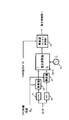
- FIG. 2 is a diagram illustrating a configuration example of a transmission apparatus including the transmission circuit according to the first embodiment.
- the transmission device 10 includes a transmission circuit 10 ⁇ / b> A, a power amplifier (power amplifier: PA, also referred to as “saturation amplifier”) 15 connected to the transmission circuit, and a bandpass filter (BPF) connected to the power amplifier 15. 16), and a transmission antenna (not shown) is connected to the output terminal of the BPF 16.
- PA power amplifier
- BPF bandpass filter
- the transmission circuit 10A is modulated input from the input terminal (complex envelope E (t)) and TPC control coefficient a preprocessing circuit 11 which K A is input, the pre-processing circuit 11 to the connected sigma-delta modulator (delta - ⁇ modulator) 12, a phase / TPC modulator 13 connected to the preprocessing circuit 11, and a multiplier 14 to which the output signal of the ⁇ - ⁇ modulator 12 and the output signal of the phase / TPC modulator 13 are input.
- the output of the multiplier 14 is input to the PA 15.
- the preprocessing circuit 11 inputs a signal indicating the amplitude component A (t) of the modulated wave e (t) to the ⁇ - ⁇ modulator 12.
- the ⁇ - ⁇ modulator 12 uses the sampling clock f s from the oscillator 18 to modulate the amplitude component A (t) into an amplitude component A ′ (t) in the PWM format.
- the amplitude component A ′ (t) is input to the multiplier 14 as a PWM signal.
- the preprocessing circuit 11 performs polar coordinate conversion of the complex envelope E (t) of the modulated wave e (t). Preprocessing circuit 11 generates a baseband signal of the instantaneous phase phi (t) and TPC-phase component I and quadrature component Q of the control coefficient K A is multiplied modulated wave e (t) of the modulated wave e (t) , Input to the phase / TPC modulator 13.
- Phase / TPC modulator 13 is a quadrature modulator, the baseband signal I, and outputs the angle-modulated wave e K? (T) orthogonal modulating the carrier f c from the oscillator 19 at Q.
- the multiplier 14 outputs a modulation signal obtained by multiplying the angle modulation wave from the phase / TPC modulator 13 and the PWM signal from the ⁇ - ⁇ modulator 12 to the power amplifier 15.
- the power amplifier 15 performs signal amplification with a predetermined transmission power and connects the output to the BPF 16.
- the BPF 16 removes signals outside the transmission band.
- the output signal of the BPF 16 is connected to a transmission antenna (not shown) and is electromagnetically radiated.
- TPC control is not performed using the amplitude modulation component, but transmission output control is performed by multiplying the angle modulation component by the TPC control coefficient K A.
- the complex envelope E K ⁇ (t) of the angle-modulated wave whose transmission output is controlled can be expressed by the following Expression 7.
- E K ⁇ (t) K A e j ⁇ (t) (Expression 7)
- an angle-modulated wave whose transmission output is controlled can be generated.
- the output signal from the phase / TPC modulator 13 is amplitude-modulated in the multiplier 14 by the PWM signal A ′ (t) from the ⁇ - ⁇ modulator 12.
- a modulated signal whose transmission output is controlled can be obtained as the output of the multiplier 14.
- the PWM signal A ′ (t) is independent of the transmission output control, and when the ratio between the quantization noise and the signal power is represented by a complex envelope, the transmission output control is expressed as shown in the following Expression 8. It turns out that it is not influenced by.
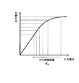
- FIG. 3 is a graph showing input / output characteristics of the power amplifier 15. In general, the input / output characteristics of the power amplifier 15 are not linear. Accordingly, amplitude control coefficients, i.e.
- TPC control coefficient K A may consider the input-output characteristic of the power amplifier 15, it can be determined as desired output is obtained. For example, the value of the input power is determined so that the output power increases at regular intervals (see FIG. 3), and the TPC control coefficient K A corresponding to the input power can be determined.
- FIG. 4 is a diagram for explaining the details of a part of the preprocessing circuit 11 and the phase / TPC modulator 13.
- the preprocessing circuit 11 includes a cosine transform unit 21 for obtaining a cosine cos ⁇ (t) with respect to the instantaneous phase ⁇ (t) of the modulated wave e (t), and a sine sin ⁇ (with respect to the instantaneous phase ⁇ (t).
- a sine transformation unit 22 for obtaining t) and multipliers 23 and 24 for multiplying cos ⁇ (t) and sin ⁇ (t) by a TPC amplitude coefficient K A are included.
- the quadrature modulator 25, that is, the phase / TPC modulator 13 performs quadrature modulation of the carrier wave f c with the baseband signals I and Q.
- a transmission output represented by Expression (8) is obtained.
- FIG. 5 shows a modification of the transmission circuit.
- a gain adjuster 26 is inserted between the quadrature modulator 25 (phase / TPC modulator 13) and the multiplier 14 instead of omitting the multipliers 23 and 24.
- a TPC control coefficient K A is input to the gain adjuster 26.
- the angle from the orthogonal modulator 25 by the gain adjuster 26 of the output side of the quadrature modulator 25 rather than the input side of the TPC amplitude coefficient K A is orthogonal modulator 25 (phase / TPC modulator 13)
- the modulated wave is multiplied.
- the angle modulation signal obtained by multiplying the quantization noise included in the PWM signal output from the ⁇ - ⁇ modulator 12 by the TPC control coefficient K A (K A ⁇ 1 (rated)) is multiplied. Multiplied by the container 14.
- the TPC control coefficient K A is multiplied not only by the signal component but also by the quantization noise (Equation 8), so that the influence of the quantization noise in the transmission output can be suppressed and the SN ratio can be suitably maintained. As a result, a high-quality signal can be transmitted.
- the quantization noise is not affected by the transmission output control, it is not necessary to use a very high oversampling frequency in advance in order to reduce the influence of the quantization noise. Output control is possible. Therefore, it is possible to realize a highly efficient linear transmission device that facilitates the implementation of the circuit and suppresses power consumption.
- Embodiment 2 will be described.
- symbol is attached
- the power efficiency of the power amplifier is highest near the maximum output, and the efficiency decreases when the transmission output is low. For this reason, when the input signal level to the power amplifier is lowered by the TPC control coefficient, the power amplification efficiency is lowered.
- Embodiment 2 demonstrates the transmitter which improves a power amplification efficiency fall.
- FIG. 6 is a diagram illustrating a configuration example of the transmission device 30 according to the second embodiment.
- the transmission device 30 is different from the first embodiment in that the transmission circuit 30A includes a DC-DC converter 31 and a power supply voltage control unit 32 in addition to the components described in the first embodiment.
- the present embodiment is different from the first embodiment in that the preprocessing circuit 11 includes a coefficient conversion unit 33 that converts the TCP control coefficient K A into a correction coefficient K A ′ that is a correction value of the TPC control coefficient.
- the power supply voltage control unit 32 includes a recording medium (for example, a memory: not shown) that stores a power supply voltage value V D corresponding to the TPC control coefficient K A. As the power supply voltage value V D , an appropriate value corresponding to the value of the TPC control coefficient K A is determined in advance and stored in the memory. Power supply voltage control unit 32 receives the pre-processing circuit 11 is input to the TPC control coefficient K A, giving a DC-DC converter 31 reads out the power supply voltage value V D corresponding to the TPC control coefficient K A.
- a recording medium for example, a memory: not shown
- the DC-DC converter 31 is controlled so that the power supply voltage of the power amplifier 15 becomes the power supply voltage value V D notified from the power supply voltage table 32. As a result, the power supply voltage V D that improves the power amplification efficiency of the power amplifier 15 is supplied to the power amplifier 15.
- the coefficient conversion unit 33 has a recording medium (memory), and a value indicating the relationship between the TPC control coefficient K A and the correction coefficient K A ′ is stored in the memory in advance.
- the TPC control coefficient K A is input to the preprocessing circuit 11, the corresponding correction coefficient K A ′ is read out.
- the read correction coefficient K A ′ is multiplied by the angle modulation component.
- the same effect as that of the first embodiment can be obtained.
- the power amplification efficiency of the power amplifier 15 can be made appropriate by further supplying the power voltage V D corresponding to the TPC control coefficient K A to the power amplifier 15.
- the TPC control coefficient multiplied by the angle modulation component can be corrected.
- one of the power control unit 32 and the coefficient conversion unit 33 can be omitted. That is, only one of power supply voltage (applied voltage) control and coefficient control may be performed.
- TPC Transmission Power Control
- TPC control coefficient K A represents the transmission output to be output as a transmission unit.
- the angle modulation component is multiplied by the TPC control coefficient. For this reason, it is considered that the power amplifier 15 operates from a low power region to a high power region.
- the TPC control coefficient is converted in consideration of the influence of the nonlinear characteristic of the power amplifier 15.
- FIG. 7 is an explanatory diagram for determining the correction coefficient.
- the input / output characteristics of the power amplifier 15 are required. Therefore, the input / output characteristics of the amplifier device, that is, the power amplifier 15 are obtained using CW (Continuous Wave) or a pulse signal (S1 in FIG. 7). Thereby, the input / output characteristics of the power amplifier 15 as shown in the graph G1 of FIG. 7 can be obtained.
- a coefficient conversion map is generated. That is, a function f (x) representing the relationship between the TPC control coefficient K A and the correction coefficient K A ′ having characteristics opposite to the input / output characteristics of the power amplifier 15 obtained in step S1 is generated (S2 in FIG. 7). ). As a result, a coefficient conversion map between K A and K A ′ as shown in the graph G2 of FIG. 7 is generated.
- the coefficient conversion map is stored in advance in a memory included in the coefficient conversion unit 33. Alternatively, the function f (x) may be stored in the memory.
- the following control can be performed. For example, it assumes that the K A that indicates the maximum transmission power is defined as K A _ MAX, the pre-processing circuit 11, K A _ MAX is input. Control by the power control unit 32 is not performed.
- the coefficient conversion unit 33 performs the following calculation using the function f (x).
- K A ′ f (K A — MAX + ( ⁇ 3)) [dB] (Formula A) In order to convert this expression A into the true value of K A ′, the following calculation is performed.
- K A ' 10 f (KA_MAX + (-3)) / 20 [true value] (Formula B) Then, the angle modulation component is multiplied by the correction coefficient K A ′ obtained by Expression B. As a result, transmission can be performed with power -3 dB lower than K A — MAX .
- the angle modulation component is multiplied by the TPC control coefficient, and the angle modulation component and the PWM signal are multiplied by the multiplier 14. This indicates that the on-state of the power amplifier is shifted from the high efficiency region to the low efficiency region. Therefore, it is possible to employ a configuration in which the voltage V Amp applied to the power amplifier is changed according to the output power so that high-efficiency operation can be achieved even at low output power.
- FIG. 8 is an explanatory diagram of voltage value determination.
- input / output characteristics of the power amplifier are obtained in advance using CW (Continuous Wave) or pulse signals at several applied voltages V Amp (S11 in FIG. 8). Thereby, the graph G3 shown in FIG. 8 is obtained.
- a function indicating the input / output characteristics of the power amplifier is obtained based on the amplification efficiency and the gain deterioration amount (graph G4 in FIG. 8), and the relationship between the output power of the power amplifier and the applied voltage V Amp is calculated using the function.
- the function shown is determined (S12 in FIG. 8). Thereby, the graph G5 of FIG. 8 is obtained.
- a function with the correction coefficient K A ′ is generated from the TPC control coefficient K A which has a characteristic opposite to that of the graph G4 (S13 in FIG. 8). Thereby, the graph G6 of FIG. 8 is obtained.
- the TPC control coefficient K A input to the preprocessing circuit 11 is determined by the output power (amplifier output) of the power amplifier.
- the memory of the power supply voltage control unit 32 stores a conversion table between the TPC control coefficient K A created based on the graph G5 and the applied voltage V Amp , that is, the power supply voltage V D.
- the power supply voltage control unit 32 can apply the applied voltage V Amp (V D ) corresponding to the TPC control coefficient K A to the power amplifier 15 via the DC-DC converter 31.
- a function, map or table based on the graph G6 is stored in the memory of the coefficient conversion unit 33, and the TPC control coefficient can be converted into a correction coefficient.
- the angle modulation component can be multiplied by the correction coefficient corresponding to the nonlinear region in the input / output characteristics of the power amplifier, and an efficient amplification operation can be performed.
- FIG. 9 is a diagram illustrating a configuration example of a transmission apparatus according to the third embodiment.
- the transmission circuit 40A of the transmission device 40 is different from the transmission circuit 30A shown in the second embodiment in that it includes a power amount detection unit 41 and an adaptive control unit 42 instead of the power control unit 32.
- the voltage applied to the power amplifier 15, that is, the power supply voltage is fixed.
- the power amount detection unit 41 detects the power amount of the transmission signal output from the BPF 16. Based on the TPC control coefficient K A and the power amount from the power amount detection unit 41, the adaptive control unit 42 determines K A ′, which is a correction value for the TPC control coefficient, and gives a conversion instruction to the coefficient conversion unit 43. .
- the coefficient conversion unit 33 converts the TPC control coefficient K A input to the preprocessing circuit 11 into a correction coefficient K A ′ in accordance with an instruction from the adaptive control unit 42. In the transmission circuit 40A, the angle modulation component is multiplied by the TPC control coefficient K A or the correction coefficient K A ′.
- the representative value of the input / output characteristics of the power amplifier is applied to the transmission device 40 during factory adjustment of the transmission device 40.
- the amplification characteristics are expected to deteriorate due to variations in device characteristics of the power amplifier, temperature changes due to use of the transmitter 40 after shipment, or changes with time. Therefore, the output of the transmission device 40 is fed back to adaptively control the conversion function of the control coefficient.
- FIG. 10 is a flowchart illustrating an operation example of the transmission circuit 40 ⁇ / b> A of the transmission device 40.
- TPC control is executed, TPC control coefficient K A in accordance with the transmission power is set (step S101).
- the TPC control coefficient K A is input to the preprocessing circuit 11.
- the coefficient conversion unit 33 converts the TPC control coefficient K A into a correction coefficient K A ′ and multiplies the angle modulation component (step S102). Thereafter, the operations described in the first embodiment are performed by the preprocessing circuit 11, the ⁇ - ⁇ modulator 12, the phase / TPC modulator 13, and the multiplier 14.
- the output signal of the multiplier 14 is amplified by the power amplifier 15, and after the component outside the transmission band is removed by the BPF 16, it is output as a transmission signal.
- the power amount detection unit 41 detects the power amount TxPW (that is, transmission output power) and inputs it to the adaptive control unit 42 (step S103).
- Adaptive control unit 42 determines, TPC control coefficient K A and the difference (error) allowable power error range of the electric energy TxPW, i.e. whether tolerance ⁇ below (step S104). If the error is less than or equal to the allowable range ⁇ (YES in S104), the process shown in FIG.
- the adaptive control unit 42 determines whether more power amount TxPW (step S105).
- the adaptive control unit 42 uses the value of the correction coefficient K A ′ included in the coefficient conversion unit 33 as the current correction coefficient K A.
- the adaptive control unit 42 uses the value of the correction coefficient K A ′ included in the coefficient conversion unit 33 as the current correction coefficient K.
- a value obtained by subtracting the predetermined value ⁇ from A ′ is set (step S107), and the process returns to step S102.
- the same effects as those of the first embodiment can be obtained. Further, according to the third embodiment, the output of the transmission device 40 is fed back, and the transmission output power amount TxPW is detected. Comparing K A is set at the determined amount of power and TPC controlling, when the allowable power error range error than ⁇ is large, if the set value is larger than the transmission output power, increased K A ', transmission output set value If it is smaller than the electric power, K A 'is controlled to be small. This makes it possible to use a TPC control coefficient suitable for the transmission output power value.
- FIG. 11 is a diagram illustrating a configuration example of a transmission apparatus according to the fourth embodiment.
- the transmission circuit 50A of the transmission device 50 includes the DC-DC converter 31 and the power supply voltage control unit 32 of the second embodiment in addition to the configuration of the transmission device 30A. Different from the circuit 40A.
- the voltage applied to the power amplifier 15, that is, the power supply voltage is variable.
- FIG. 12 is a flowchart illustrating an operation example of the transmission circuit 50 ⁇ / b> A of the transmission device 50.
- TPC control is executed, TPC control coefficient K A in accordance with the transmission power is set (step S201).
- the TPC control coefficient K A is input to the preprocessing circuit 11.
- the output signal of the multiplier 14 is amplified by the power amplifier 15, and after the component outside the transmission band is removed by the BPF 16, it is output as a transmission signal.
- a part of the transmission signal output from the BPF 16 is input to the power amount detection unit 41 through a feedback path.
- the power amount detection unit 41 detects the power amount TxPW (that is, transmission output power) and inputs it to the adaptive control unit 42 (step S203).
- Adaptive control unit 42 determines, TPC control coefficient K A and the difference (error .DELTA.Pi) is allowable power error range of the electric energy TxPW, i.e. whether tolerance ⁇ below (step S204). If the error is less than or equal to the allowable range ⁇ (YES in S204), the process proceeds to step S210.
- the adjustment of the control coefficient is executed prior to the control of the applied voltage. That is, the adaptive control unit 42, the current TPC control coefficient K A determines whether more power amount TxPW (step S205).
- the adaptive control unit 42 uses the value of the correction coefficient K A ′ included in the coefficient conversion unit 33 as the current correction coefficient K A.
- a value obtained by adding a predetermined value ⁇ to ' is set (step S206).
- the adaptive control unit 42 uses the value of the correction coefficient K A ′ included in the coefficient conversion unit 33 as the current correction coefficient K.
- a value obtained by subtracting the predetermined value ⁇ from A ′ is set (step S207).
- step S206 or S207 ends, the processing of steps S202 to S205 is repeated.
- step S205A if TPC control coefficient K A is greater than the amount of power TxPW (YES in S205A), the adaptive control unit 42, the power supply voltage control unit 32 hold The value of the applied voltage Vamp to be set is set to a value obtained by adding a predetermined value ⁇ V to the current applied voltage (step S208).
- step S209 the value of the applied voltage Vamp supply voltage control unit 32 holds, from the current applied voltage A value obtained by subtracting the predetermined value ⁇ is set (step S209).
- step S210 when the process proceeds to step S210, that is, when the error exceeds the allowable range, the applied voltage control is executed. That is, the adaptive control unit 42 sets the value of the applied voltage Vamp held by the power supply voltage control unit 32 to a value obtained by subtracting the predetermined value ⁇ from the current applied voltage.
- step S202A the same processing as in step S202 is performed (S202A), the electric energy TxPW is detected (step S203A), and it is determined whether or not the error ⁇ Pi is less than the allowable range ⁇ (step S211).
- the adaptive control unit 42 sets the value of the applied voltage Vamp held by the power supply voltage control unit 32 to a value obtained by adding a predetermined value ⁇ from the current applied voltage.
- step S212 the same processing as step S202 is performed, and the processing of FIG. However, the processing after step S203A may be executed.
- the adaptive control unit 42 changes the value of the applied voltage Vamp held by the power supply voltage control unit 32 from the current applied voltage to a predetermined value ⁇ . Is set to a value obtained by subtracting (step S214), and the process returns to step S202A.
- the same effect as that of the first embodiment can be obtained. Furthermore, according to the fourth embodiment, as in the third embodiment, the output of the transmission apparatus is fed back and the transmission output power amount is detected. The obtained power amount is compared with K A set by TPC control, and when the error is larger than the allowable power error range ⁇ , the correction coefficient K A ′ is first controlled. If the TPC control coefficient K A is larger than the transmission output power, K A ′ is increased, and if the set value is smaller than the transmission output power, control is performed to decrease K A ′.
- K A ′ and V Amp are set again, and if the error is larger than the allowable power error range ⁇ , the applied voltage V Amp of the amplifier device (power amplifier 15) is controlled. If K A is larger than the transmission output power, control is performed so that V Amp is increased, and if K A is smaller than the transmission output power, V Amp is decreased. If the error does not fall within the allowable power error range ⁇ , the above operation is repeated.
- control is performed in a direction to reduce the voltage as much as possible (low voltage) for high efficiency operation, and the control is repeated until an appropriate voltage value that does not exceed the allowable power error range is obtained.
- This makes it possible to use a TPC control coefficient suitable for the transmission output power value.
Landscapes
- Engineering & Computer Science (AREA)
- Computer Networks & Wireless Communication (AREA)
- Signal Processing (AREA)
- Power Engineering (AREA)
- Amplifiers (AREA)
- Transmitters (AREA)
- Digital Transmission Methods That Use Modulated Carrier Waves (AREA)
Abstract
送信回路は、変調信号の振幅変調成分をΣ-Δ変調してパルス幅変調信号を出力するΣ-Δ変調器と、電力増幅器での送信出力に応じた送信出力制御係数を前記変調信号に乗じることにより得られる信号の角度変調成分信号を生成する角度変調部と、前記パルス幅変調信号と前記角度変調成分信号とを乗じ、当該乗算結果を前記電力増幅器への出力信号として出力する乗算器とを含む。
Description
本発明は、送信回路に関する。
第3世代(3G)やこれからのワイヤレス通信の主流である線形変調システムでは高い電力効率でひずみ無く増幅することができる送信装置の実現が望まれている。線形変調は包絡線が変動するため、信号のピークと平均電力の比(Peak to Average Ratio)を考慮して増幅器を設計/動作させている。このため、送信装置の電力効率が低いという問題があった。
従来技術の一つとして、図1に示されるような送信回路装置がある(例えば、特許文献1を参照)。この送信回路装置の技術では、図1に示されるように、データ発生器5が、変調波の角度成分たる角度変調データと変調波の振幅成分たる振幅変調データとをそれぞれ出力する。ここで、周波数fc の搬送波c(t)は、下記の式1で表すことができる。
c(t)=cos(2πfct)=Re[ej2πfct] ・・・(式1)
搬送波c(t)に対する変調波e(t)は、複素包絡線E(t)を用いて、以下の式2、式3で表すことができる。
搬送波c(t)に対する変調波e(t)は、複素包絡線E(t)を用いて、以下の式2、式3で表すことができる。
e(t)=A(t){cos(φ(t))・cos(2πfct)-sin(φ(t))・sin(2πfct))
=Re[E(t)ej2πfct] ・・・(式2)
E(t)=A(t)・ejφ(t) ・・・(式3)
A(t)は、変調波の振幅(振幅成分)を表す。φ(t)は位相(角度成分)を表し、周波数は位相の微分であるため、両者は一般に角度成分として扱うことができる。
=Re[E(t)ej2πfct] ・・・(式2)
E(t)=A(t)・ejφ(t) ・・・(式3)
A(t)は、変調波の振幅(振幅成分)を表す。φ(t)は位相(角度成分)を表し、周波数は位相の微分であるため、両者は一般に角度成分として扱うことができる。
図1に示す周波数変調器1は、角度成分φ(t)で変調された信号を発生する。一方、振幅成分A(t)は、Σ-Δ変調器(またはΔ-Σ変調器)3でパルス幅変調(PWM)信号に変換される。このPWM 形式に変換された振幅成分、すなわちPWM信号A'(t) と、角度変調された信号とが振幅変調器2で変調される。振幅変調器2の出力は、一定振幅の角度変調波がPWM信号の“1”又は“0”に従ってオン又はオフされた信号となる。
このような振幅変調器2の出力信号の振幅は0又は一定値である。従って、出力信号が振幅変調器2の後段に置かれた図示しないB級又はC級の電力増幅器で増幅されても、ひずみが発生せず、且つB級又はC級の電力増幅器が本来備えている高い電力効率で信号を送信することができる。
但し、このままでは、PWM信号に付随する量子化雑音が送信帯域外に雑音として出力されるおそれがある。すなわち、PWM信号A'(t) は元の振幅成分A(t) に対して量子化雑音に対応する誤差QA(t) が加わったものであり、以下の式4で表すことができる。
A'(t) =A(t)+QA (t)・・・ (式4)
このようなPWM信号A'(t)を用い、振幅変調器2で一定振幅の角度変調波を振幅変調すると、振幅変調器2の出力にも量子化雑音Q(t)で振幅変調された量子化雑音が発生する。量子化雑音の大部分は送信帯域外成分となるため、バンドパスフィルタ(BPF)4で減衰させ、量子化雑音の残留成分QA’(t)を小さくすることが可能である。
このようなPWM信号A'(t)を用い、振幅変調器2で一定振幅の角度変調波を振幅変調すると、振幅変調器2の出力にも量子化雑音Q(t)で振幅変調された量子化雑音が発生する。量子化雑音の大部分は送信帯域外成分となるため、バンドパスフィルタ(BPF)4で減衰させ、量子化雑音の残留成分QA’(t)を小さくすることが可能である。
このようにして、図1に示した送信回路装置(従来技術)では、包絡線変動の大きな送信信号を高効率かつひずみ無く送信することができる。
上述したΣ-Δ変調器による変調の過程では、量子化雑音が発生する。そのため送信信号の平均電力を変更(出力電力を下げるなど)したい場合、信号の振幅制御により電力制御を実現しようとすると、送信帯域外の雑音電力の規格を満足することが難しくなる。
本発明の一態様の目的は、送信信号の電力と送信帯域外の電力との比を適正範囲内に抑えた送信回路を提供することである。
本発明の一態様は、送信回路である。この送信回路は、変調信号の振幅変調成分をΣ-Δ変調してパルス幅変調信号を出力するΣ-Δ変調器と、
電力増幅器での送信出力に応じた送信出力制御係数を前記変調信号に乗じることにより得られる信号の角度変調成分信号を生成する角度変調部と、
前記パルス幅変調信号と前記角度変調成分信号とを乗じ、当該乗算結果を前記電力増幅器への出力信号として出力する乗算器と
を含む。
電力増幅器での送信出力に応じた送信出力制御係数を前記変調信号に乗じることにより得られる信号の角度変調成分信号を生成する角度変調部と、
前記パルス幅変調信号と前記角度変調成分信号とを乗じ、当該乗算結果を前記電力増幅器への出力信号として出力する乗算器と
を含む。
本発明の一態様によれば、送信信号の電力と送信帯域外の電力との比を適正範囲内に抑える送信回路を実現することができる。
以下、図面を参照して本発明の実施形態を説明する。実施形態の構成は例示であり、本発明は実施形態の構成に限定されない。
<実施形態の経緯>
携帯電話システムでは基地局と端末との距離や周囲の電波環境に応じて、送信出力を適切な電力に制御する送信出力制御(Transmission Power Control:TPC)が行われる。図1に示した従来技術の構成で送信出力を変更する場合、振幅成分A(t)にTPC制御係数KA(但しKA≦1、1は定格出力)を乗算したデータを用いてPWM信号A"(t)を生成する方法が考えられる。PWM信号A"(t)は、以下の式5で表すことができる。
携帯電話システムでは基地局と端末との距離や周囲の電波環境に応じて、送信出力を適切な電力に制御する送信出力制御(Transmission Power Control:TPC)が行われる。図1に示した従来技術の構成で送信出力を変更する場合、振幅成分A(t)にTPC制御係数KA(但しKA≦1、1は定格出力)を乗算したデータを用いてPWM信号A"(t)を生成する方法が考えられる。PWM信号A"(t)は、以下の式5で表すことができる。
A"(t) =KAA(t)+QA(t) ・・・(式5)
また、式5に示したPWM信号A"(t)を用いて、変調波(BPF4への入力)の複素包絡線E"(t)を表すと以下の式6となる。
また、式5に示したPWM信号A"(t)を用いて、変調波(BPF4への入力)の複素包絡線E"(t)を表すと以下の式6となる。
E"(t)=A"(t)・ejφ(t)=(KAA(t)+QA(t))ejφ(t)
=KAA(t) ejφ(t)+QA(t)ejφ(t) ・・・(式6)
式6より、量子化雑音に対応する誤差QA(t)の電力はTPC制御係数KAによらずほぼ一定になることが分かる。一方、送信信号電力はTPC制御係数KAによって減少するため、信号対雑音比(SN比)がKAに比例して劣化し、BPF4の出力のSN比も同様に劣化する。
=KAA(t) ejφ(t)+QA(t)ejφ(t) ・・・(式6)
式6より、量子化雑音に対応する誤差QA(t)の電力はTPC制御係数KAによらずほぼ一定になることが分かる。一方、送信信号電力はTPC制御係数KAによって減少するため、信号対雑音比(SN比)がKAに比例して劣化し、BPF4の出力のSN比も同様に劣化する。
送信帯域外の雑音レベルは送信出力に応じて低くすることが義務付けられており、従来技術の送信回路装置では、雑音レベルに対する要求を十分満足することが困難となる。また、送信信号に含まれる雑音(Error Vector Magnitude:EVM)が増加し、信号の品質が劣化するという問題もある。
実施形態は、上述した問題に鑑み、送信出力を可変にした場合でも、送信帯域外の雑音を適正範囲内に抑えることができる送信回路について説明する。
<実施形態1>
図2は、実施形態1における送信回路を含む送信装置の構成例を示す図である。図2において、送信装置10は、送信回路10Aと、送信回路に接続された電力増幅器(パワーアンプ:PA、「飽和増幅器」ともいう)15と、電力増幅器15に接続されたバンドパスフィルタ(BPF)16とを備え、BPF16の出力端子には、図示しない送信アンテナが接続されている。
図2は、実施形態1における送信回路を含む送信装置の構成例を示す図である。図2において、送信装置10は、送信回路10Aと、送信回路に接続された電力増幅器(パワーアンプ:PA、「飽和増幅器」ともいう)15と、電力増幅器15に接続されたバンドパスフィルタ(BPF)16とを備え、BPF16の出力端子には、図示しない送信アンテナが接続されている。
送信回路10Aは、入力端子から変調入力(複素包絡線E(t))及びTPC制御係数KAが入力される前処理回路11と、前処理回路11に接続されたΣ-Δ変調器(Δ-Σ変調器)12と、前処理回路11に接続された位相/TPC変調器13と、Σ-Δ変調器12の出力信号及び位相/TPC変調器13の出力信号が入力される乗算器14とを備え、乗算器14の出力はPA15に入力される。
前処理回路11は、変調波e(t)の振幅成分A(t)を示す信号をΣ-Δ変調器12に入力する。Σ-Δ変調器12は、発振器18からの標本化クロックfsを用いて振幅成分A(t)をPWM形式の振幅成分A’(t)に変調する。振幅成分A’(t)はPWM信号として乗算器14に入力される。
また、前処理回路11は、変調波e(t)の複素包絡線E(t)の極座標変換を行う。前処理回路11は、変調波e(t)の瞬時位相φ(t)及びTPC制御係数KAが乗算された変調波e(t)の同相成分I及び直交成分Qのベースバンド信号を生成し、位相/TPC変調器13に入力する。
位相/TPC変調器13は、直交変調器であり、ベースバンド信号I,Qで発振器19からの搬送波fcを直交変調した角度変調波eKφ(t)を出力する。乗算器14は、位相/TPC変調器13からの角度変調波とΣ-Δ変調器12からのPWM信号とを乗算した変調信号を電力増幅器15に出力する。電力増幅器15は、所定の送信電力で信号増幅を行い、出力をBPF16に接続する。BPF16は、送信帯域外の信号を除去する。BPF16の出力信号は、図示しない送信アンテナに接続され、電磁放射される。
実施形態1では、振幅変調成分を用いてTPC制御を行うのではなく、角度変調成分にTPC制御係数KAを乗算することで送信出力制御を行う。この送信出力制御された角度変調波の複素包絡線EKφ(t)は以下の式7で表すことができる。
EKφ(t)=KAejφ(t) ・・・(式7)
複素包絡線EKφ(t)を位相/TPC変調器13に入力して搬送波を変調することで、送信出力制御された角度変調波を発生することができる。位相/TPC変調器13からの出力信号は、乗算器14において、Σ-Δ変調器12からのPWM信号A'(t)で振幅変調される。これによって、乗算器14の出力として、送信出力制御された変調信号を得ることができる。この場合、PWM信号A'(t)は送信出力制御から独立しており、量子化雑音と信号電力との比を複素包絡線で表示すると、以下の式8で表されるように送信出力制御の影響を受けないことがわかる。
複素包絡線EKφ(t)を位相/TPC変調器13に入力して搬送波を変調することで、送信出力制御された角度変調波を発生することができる。位相/TPC変調器13からの出力信号は、乗算器14において、Σ-Δ変調器12からのPWM信号A'(t)で振幅変調される。これによって、乗算器14の出力として、送信出力制御された変調信号を得ることができる。この場合、PWM信号A'(t)は送信出力制御から独立しており、量子化雑音と信号電力との比を複素包絡線で表示すると、以下の式8で表されるように送信出力制御の影響を受けないことがわかる。
E'(t)=A'(t)・KAejφ(t)=KA(A(t)+QA(t))ejφ(t)
=KAA(t) ejφ(t) +KAQA(t)ejφ(t) ・・・(式8)
図2の構成例では、電力増幅器15への入力信号全体にTPC制御係数KAという振幅係数が掛けられる。これによって、電力増幅器15の出力が変化する。図3は、電力増幅器15の入出力特性を示すグラフである。一般に、電力増幅器15の入出力特性は線形ではない。従って、振幅制御係数、すなわちTPC制御係数KAは電力増幅器15の入出力特性を考慮し、所望の出力が得られるように決定することができる。例えば、出力電力が一定の間隔で増加するように入力電力の値が決められ(図3参照)、入力電力に応じたTPC制御係数KAが決定されることができる。
=KAA(t) ejφ(t) +KAQA(t)ejφ(t) ・・・(式8)
図2の構成例では、電力増幅器15への入力信号全体にTPC制御係数KAという振幅係数が掛けられる。これによって、電力増幅器15の出力が変化する。図3は、電力増幅器15の入出力特性を示すグラフである。一般に、電力増幅器15の入出力特性は線形ではない。従って、振幅制御係数、すなわちTPC制御係数KAは電力増幅器15の入出力特性を考慮し、所望の出力が得られるように決定することができる。例えば、出力電力が一定の間隔で増加するように入力電力の値が決められ(図3参照)、入力電力に応じたTPC制御係数KAが決定されることができる。
上述したように、位相/TPC変調器13として、直交変調器を用いることができる。図4は、前処理回路11の一部と位相/TPC変調器13との詳細を説明する図である。図4に示すように、前処理回路11は、変調波e(t)の瞬時位相φ(t)に対する余弦cosφ(t)を求めるコサイン変換部21と、瞬時位相φ(t)に対する正弦sinφ(t)を求めるサイン変換部22と、cosφ(t)及びsinφ(t)に対してTPC振幅係数KAを乗算する乗算器23及び24を含んでいる。
このような構成によって、乗算器23からは同相成分Iのベースバンド信号(同相成分I=KAcosφ(t))が出力され、乗算器24からは直交成分Qのベースバンド信号(直交成分Q=KAsinφ(t))が出力される。直交変調器25、すなわち位相/TPC変調器13は、搬送波fcをベースバンド信号I,Qで直交変調する。この結果、直交変調器25の出力信号として、複素包絡線がEKφ(t)=KAejφ(t)なる送信出力制御された角度変調波を発生することができる。この角度変調波に乗算器14でPWM信号A'(t)を乗算することで、式(8)に示す送信出力が得られる。
図2及び図4に示す構成は、図5に示すように変形が可能である。図5は、送信回路の変形例を示す。図5に示す例では、乗算器23,24が省略される代わりに、直交変調器25(位相/TPC変調器13)と乗算器14との間にゲイン調整器26が挿入されている。このゲイン調整器26に、TPC制御係数KAが入力される。
図5に示す例では、TPC振幅係数KAが直交変調器25(位相/TPC変調器13)の入力側ではなく直交変調器25の出力側のゲイン調整器26で直交変調器25からの角度変調波に乗算される。
実施形態1によれば、Σ-Δ変調器12から出力されるPWM信号に含まれる量子化雑音に対し、TPC制御係数KA(KA≦1(定格))を乗算した角度変調信号が乗算器14で乗じられる。これによって、TPC制御係数KAが信号成分だけでなく量子化雑音にも乗じられる(式8)ことにより、送信出力における量子化雑音の影響を抑え、SN比を好適に保つことができる。その結果、品質の良い信号を送信することができる。
また、実施形態1によれば、量子化雑音が送信出力制御の影響を受けないため、量子化雑音の影響を軽減するために予め非常に高いオーバーサンプリング周波数を用いる必要が無く、広い範囲の送信出力制御が可能となる。したがって、回路の実現が容易になると共に、消費電力を抑えた、高効率の線形送信装置を実現することができる。
<実施形態2>
次に、実施形態2について説明する。実施形態1と同様の構成については、同一の符号を付して説明を省略する。一般に、電力増幅器の電力効率は、最大出力付近が最も高く、送信出力が低い状態では、効率が低下する。このため、電力増幅器への入力信号レベルをTPC制御係数によって下げると、電力増幅効率が低下する。実施形態2は、電力増幅効率低下を改善する送信装置について説明する。
次に、実施形態2について説明する。実施形態1と同様の構成については、同一の符号を付して説明を省略する。一般に、電力増幅器の電力効率は、最大出力付近が最も高く、送信出力が低い状態では、効率が低下する。このため、電力増幅器への入力信号レベルをTPC制御係数によって下げると、電力増幅効率が低下する。実施形態2は、電力増幅効率低下を改善する送信装置について説明する。
図6は、実施形態2における送信装置30の構成例を示す図である。送信装置30は、送信回路30Aが、実施形態1で説明した構成要素に加えて、DC-DC変換器31及び電源電圧制御部32を備える点で、実施形態1と異なる。また、前処理回路11がTCP制御係数KAをTPC制御係数の補正値である補正係数KA'に変換する係数変換部33を含む点で、実施形態1と異なる。
前処理回路11には、送信出力制御を考慮したTPC制御係数KAが入力される。すなわち、送信電力に応じた値のTPC制御係数KAが入力される。電源電圧制御部32は、TPC制御係数KAに対応する電源電圧値VDを記憶した記録媒体(例えばメモリ:図示せず)を備えている。電源電圧の値VDとして、TPC制御係数KAの値に対応する適切な値が予め決定され、メモリに格納される。電源電圧制御部32は、前処理回路11に入力されるTPC制御係数KAを受け取り、TPC制御係数KAに対応する電源電圧値VDを読み出してDC-DC変換器31に与える。
DC-DC変換器31は、電力増幅器15の電源電圧が電源電圧テーブル32から通知された電源電圧値VDとなるように制御される。これによって、電力増幅器15の電力増幅効率が良好となる電源電圧VDが電力増幅器15に供給される。
一方、係数変換部33は、記録媒体(メモリ)を有しており、TPC制御係数KAと補正係数KA'との関係を示す値が予めメモリに格納されている。前処理回路11にTPC制御係数KAが入力されると、対応する補正係数KA'を読み出す。読み出された補正係数KA'は、角度変調成分に乗算される。
実施形態2によれば、実施形態1と同様の作用効果を得ることができる。実施形態2によれば、さらに、TPC制御係数KAに応じた電源電圧VDが電力増幅器15に供給されることで、電力増幅器15の電力増幅効率を適切にすることができる。また、角度変調成分に乗じるTPC制御係数を補正することができる。
なお、実施形態2において、電力制御部32と係数変換部33との一方は省略が可能である。すなわち、電源電圧(印加電圧)制御と係数制御との一方のみが実施されるようにしても良い。
<<具体例1>>
実施形態2に関して、TPC制御係数KAから補正係数KA'を決定する具体的手法について説明する。TPC(Transmission Power Control)は送信出力電力値の制御であり、TPC制御係数KAは送信ユニットとして出力する送信出力を表している。実施形態2の送信回路30Aでは、角度変調成分にTPC制御係数を乗算する。このため、電力増幅器15が電力の低い領域から高い領域まで動作することを考慮する。特に、動作点が電力増幅器15の飽和領域に位置する場合には、電力増幅器15の非線形特性の影響を考慮したTPC制御係数の変換を行う。
実施形態2に関して、TPC制御係数KAから補正係数KA'を決定する具体的手法について説明する。TPC(Transmission Power Control)は送信出力電力値の制御であり、TPC制御係数KAは送信ユニットとして出力する送信出力を表している。実施形態2の送信回路30Aでは、角度変調成分にTPC制御係数を乗算する。このため、電力増幅器15が電力の低い領域から高い領域まで動作することを考慮する。特に、動作点が電力増幅器15の飽和領域に位置する場合には、電力増幅器15の非線形特性の影響を考慮したTPC制御係数の変換を行う。
図7は、補正係数決定の説明図である。TPC制御係数KAから補正係数KA'への変換においては、電力増幅器15の入出力特性が必要となる。このため、アンプデバイス、すなわち電力増幅器15の入出力特性をCW(Continuous Wave)或いはパルス信号を用いて求める(図7のS1)。これにより、図7のグラフG1に示すような電力増幅器15の入出力特性を得ることができる。
次に、係数変換マップを生成する。すなわち、ステップS1で得られた電力増幅器15の入出力特性と逆の特性を有するTPC制御係数KAと補正係数KA'との関係を表す関数f(x)を生成する(図7のS2)。これによって、図7のグラフG2に示すようなKA-KA'間の係数変換マップが生成される。係数変換マップは、係数変換部33が有するメモリに予め格納される。或いは、関数f(x)がメモリに格納されていても良い。
また、以下のような制御を行うことができる。例えば、最大送信出力を示すKAをKA_MAXと定義し、前処理回路11には、KA_MAXが入力されると仮定する。電力制御部32による制御は行われない。ここで、KA_MAXよりも-3dB低い電力で送信を行う場合には、係数変換部33は、関数f(x)を用いて以下の計算を行う。
KA'=f(KA_MAX+(-3)) [dB] ・・・(式A)
この式AをKA'の真値に変換するために、以下の計算を行う。
この式AをKA'の真値に変換するために、以下の計算を行う。
KA'=10f(KA_MAX+(-3))/20 [真値] ・・・(式B)
そして、式Bにて得られた補正係数KA'が角度変調成分に乗算される。これによって、KA_MAXよりも-3dB低い電力で送信を行うことができる。
そして、式Bにて得られた補正係数KA'が角度変調成分に乗算される。これによって、KA_MAXよりも-3dB低い電力で送信を行うことができる。
<<具体例2>>
次に、TPC制御係数KAから電力増幅器15(アンプ)に印加する電力値VDを決定する具体的手法について説明する。アンプデバイス、すなわち電力増幅器は、飽和領域において高い増幅効率で動作する。しかし、低い電力を出力する場合には、増幅器の効率が低くなる。Σ-Δ変調方式による電力増幅器への入力信号は2値であり、PWM信号がオン“1”のときに電力増幅器はオン状態となり、効率の高い飽和領域で動作する。これに対し、PWM信号がオフ“0”のときに電力増幅器はオフ状態となる。オフ状態での消費電力は“0”である。
次に、TPC制御係数KAから電力増幅器15(アンプ)に印加する電力値VDを決定する具体的手法について説明する。アンプデバイス、すなわち電力増幅器は、飽和領域において高い増幅効率で動作する。しかし、低い電力を出力する場合には、増幅器の効率が低くなる。Σ-Δ変調方式による電力増幅器への入力信号は2値であり、PWM信号がオン“1”のときに電力増幅器はオン状態となり、効率の高い飽和領域で動作する。これに対し、PWM信号がオフ“0”のときに電力増幅器はオフ状態となる。オフ状態での消費電力は“0”である。
実施形態1,2における送信装置では、TPC制御係数が角度変調成分に乗算され、この角度変調成分とPWM信号とが乗算器14で乗算される。これは、電力増幅器のオン状態を高効率領域から効率の低い領域にシフトして使用することを示している。そこで、低い出力電力時においても高効率動作となるように、出力電力に応じて電力増幅器への印加電圧VAmpを変化させる構成を採用することができる。
図8は、電圧値決定の説明図である。最初に、幾つかの印加電圧VAmpにおいて、CW(Continuous Wave)或いはパルス信号を用いて予め電力増幅器の入出力特性を求める(図8のS11)。これにより、図8に示すグラフG3が得られる。
次に、増幅効率とゲイン劣化量に基づき、電力増幅器の入出力特性を示す関数を求め(図8のグラフG4)、当該関数を用いて電力増幅器の出力電力と印加電圧VAmpとの関係を示す関数を決定する(図8のS12)。これによって、図8のグラフG5が得られる。一方、グラフG4と逆特性となるようなTPC制御係数KAから補正係数KA'との関数を生成する(図8のS13)。これによって、図8のグラフG6が得られる。
前処理回路11に入力されるTPC制御係数KAは、電力増幅器の出力電力(アンプ出力)によって決まる。電源電圧制御部32のメモリには、グラフG5を元に作成されたTPC制御係数KAから印加電圧VAmp、すなわち電源電圧VDとの変換テーブルが格納される。これによって、電源電圧制御部32は、TPC制御係数KAに応じた印加電圧VAmp(VD)をDC-DC変換器31を介して電力増幅器15に印加することができる。
また、グラフG6に基づく関数、マップ又はテーブルが係数変換部33のメモリに格納され、TPC制御係数を補正係数に変換することができる。これによって、電力増幅器の入出力特性における非線形領域に対応した補正係数を角度変調成分に乗じることが可能となり、効率の良い増幅動作を行うことが可能となる。
<実施形態3>
次に、実施形態3について説明する。実施形態1,2と同様の構成については、同一の符号を付して説明を省略する。図9は、実施形態3における送信装置の構成例を示す図である。図9において、送信装置40の送信回路40Aは、電力制御部32の代わりの電力量検出部41及び適応制御部42を備える点で、実施形態2に示した送信回路30Aと異なっている。送信回路40では、電力増幅器15への印加電圧、すなわち電源電圧は固定である。
次に、実施形態3について説明する。実施形態1,2と同様の構成については、同一の符号を付して説明を省略する。図9は、実施形態3における送信装置の構成例を示す図である。図9において、送信装置40の送信回路40Aは、電力制御部32の代わりの電力量検出部41及び適応制御部42を備える点で、実施形態2に示した送信回路30Aと異なっている。送信回路40では、電力増幅器15への印加電圧、すなわち電源電圧は固定である。
電力量検出部41は、BPF16から出力される送信信号の電力量を検出する。適応制御部42は、TPC制御係数KAと電力量検出部41からの電力量とに基づき、TPC制御係数の補正値であるKA'を決定し、係数変換部43に変換の指示を与える。係数変換部33は、適応制御部42からの指示に従って、前処理回路11に入力されるTPC制御係数KAを補正係数KA'に変換する。送信回路40Aでは、TPC制御係数KA又は補正係数KA'が角度変調成分に乗算される。
以下、実施形態3の動作例について説明する。例えば、送信装置40の工場調整時において、電力増幅器の入出力特性の代表値が送信装置40に適用されると仮定する。この場合、電力増幅器のデバイス特性のばらつきや、出荷後の送信装置40の使用による温度変化、或いは経時変化により増幅特性の劣化が予想される。そこで、送信装置40の出力をフィードバックし、制御係数の変換関数を適応制御する。
図10は、送信装置40の送信回路40Aの動作例を示すフローチャートである。送信装置40の動作時には、TPC制御が実行され、送信電力に応じたTPC制御係数KAが設定される(ステップS101)。TPC制御係数KAは前処理回路11に入力される。
前処理回路11では、係数変換部33によってTPC制御係数KAが補正係数KA'に変換され、角度変調成分に乗算される(ステップS102)。その後、実施形態1で説明した動作が前処理回路11,Σ-Δ変調器12,位相/TPC変調器13,乗算器14で行われる。乗算器14の出力信号は、電力増幅器15で電力増幅され、BPF16で送信帯域外成分が除去された後、送信信号として出力される。
BPF16から出力される送信信号の一部は、フィードバック経路を通って電力量検出部41に入力される。電力量検出部41は、電力量TxPW(すなわち送信出力電力)を検出し、適応制御部42に入力する(ステップS103)。
適応制御部42は、TPC制御係数KAと電力量TxPWとの差分(誤差)が許容電力誤差範囲、すなわち許容範囲δ以下か否かを判定する(ステップS104)。誤差が許容範囲δ以下の場合(S104のYES)には、図10に示す処理を終了する。
これに対し、誤差が許容範囲δを上回る場合(S104のNO)には、適応制御部42は、現在のTPC制御係数KAが電力量TxPWより大きいか否かを判定する(ステップS105)。
このとき、TPC制御係数KAが電力量TxPWより大きい場合(S105のYES)には、適応制御部42は、係数変換部33が有する補正係数KA'の値を、現在の補正係数KA'に所定値Δσを加えた値に設定し(ステップS106)、処理をステップS102に戻す。これに対し、TPC制御係数KAが電力量TxPW以下の場合(S105のNO)には、適応制御部42は、係数変換部33が有する補正係数KA'の値を、現在の補正係数KA'から所定値Δσを減じた値に設定し(ステップS107)、処理をステップS102に戻す。
実施形態3によれば、実施形態1と同様の作用効果を得ることができる。さらに、実施形態3によれば、送信装置40の出力をフィードバックし、送信出力電力量TxPWを検出する。求めた電力量とTPC制御で設定されるKAを比較し、許容電力誤差範囲δより誤差が大きい場合において、設定値が送信出力電力より大きければ、KA'を大きく、設定値が送信出力電力より小さければKA'を小さくするよう制御する。これによって、送信出力電力値に適したTPC制御係数を使用することが可能となる。
<実施形態4>
次に、実施形態4について説明する。実施形態1,2,3と同様の構成については、同一の符号を付して説明を省略する。図11は、実施形態4における送信装置の構成例を示す図である。図11において、送信装置50の送信回路50Aは、送信装置30Aの構成に加えて、実施形態2のDC-DC変換器31及び電源電圧制御部32を備える点で、実施形態3に示した送信回路40Aと異なっている。送信回路50では、電力増幅器15への印加電圧、すなわち電源電圧は可変である。
次に、実施形態4について説明する。実施形態1,2,3と同様の構成については、同一の符号を付して説明を省略する。図11は、実施形態4における送信装置の構成例を示す図である。図11において、送信装置50の送信回路50Aは、送信装置30Aの構成に加えて、実施形態2のDC-DC変換器31及び電源電圧制御部32を備える点で、実施形態3に示した送信回路40Aと異なっている。送信回路50では、電力増幅器15への印加電圧、すなわち電源電圧は可変である。
図12は、送信装置50の送信回路50Aの動作例を示すフローチャートである。送信装置50の動作時には、TPC制御が実行され、送信電力に応じたTPC制御係数KAが設定される(ステップS201)。TPC制御係数KAは前処理回路11に入力される。
前処理回路11では、係数変換部33によってTPC制御係数KAが補正係数KA'に変換され、角度変調成分に乗算される。その後、実施形態1で説明した動作が前処理回路11,Σ-Δ変調器12,位相/TPC変調器13,乗算器14で行われる。一方で、電源電圧制御部32によって、アンプデバイスたる電力増幅器15に対し、TPC制御係数KAに応じた印加電圧VampがDC-DC変換器31を介して印加される(ステップS202)。
乗算器14の出力信号は、電力増幅器15で電力増幅され、BPF16で送信帯域外成分が除去された後、送信信号として出力される。BPF16から出力される送信信号の一部は、フィードバック経路を通って電力量検出部41に入力される。電力量検出部41は、電力量TxPW(すなわち送信出力電力)を検出し、適応制御部42に入力する(ステップS203)。
適応制御部42は、TPC制御係数KAと電力量TxPWとの差分(誤差ΔPi)が許容電力誤差範囲、すなわち許容範囲δ以下か否かを判定する(ステップS204)。誤差が許容範囲δ以下の場合(S204のYES)には、処理がステップS210に進む。
これに対し、誤差が許容範囲δを上回る場合(S204のNO)には、制御係数の調整が印加電圧の制御に先んじて実行される。すなわち、適応制御部42は、現在のTPC制御係数KAが電力量TxPWより大きいか否かを判定する(ステップS205)。
このとき、TPC制御係数KAが電力量TxPWより大きい場合(S205のYES)には、適応制御部42は、係数変換部33が有する補正係数KA'の値を、現在の補正係数KA'に所定値Δσを加えた値に設定する(ステップS206)。これに対し、TPC制御係数KAが電力量TxPW以下の場合(S205のNO)には、適応制御部42は、係数変換部33が有する補正係数KA'の値を、現在の補正係数KA'から所定値Δσを減じた値に設定する(ステップS207)。
ステップS206又はS207が終了すると、ステップS202~S205の処理が繰り返される。二回目のステップS205(図12で“S205A”と表記)において、TPC制御係数KAが電力量TxPWより大きい場合(S205AのYES)には、適応制御部42は、電源電圧制御部32が保持する印加電圧Vampの値を、現在の印加電圧に所定値ΔVを加えた値に設定する(ステップS208)。これに対し、TPC制御係数KAが電力量TxPW以下の場合(S205AのNO)には、適応制御部42は、電源電圧制御部32が保持する印加電圧Vampの値を、現在の印加電圧から所定値Δσを減じた値に設定する(ステップS209)。ステップS208又はS209の処理が終了すると、処理がステップS202に戻る。
ところで、処理がステップS210に進んだ場合、すなわち、誤差が許容範囲を超えている場合には、印加電圧制御が実行される。すなわち、適応制御部42は、電源電圧制御部32が保持する印加電圧Vampの値を、現在の印加電圧から所定値Δσを減じた値に設定する。
その後、ステップS202と同様の処理が行われ(S202A)、電力量TxPWが検出され(ステップS203A)、誤差ΔPiが許容範囲δ未満か否かを判定する(ステップS211)。誤差が許容範囲δを上回る場合(S211のNO)には、適応制御部42は、電源電圧制御部32が保持する印加電圧Vampの値を、現在の印加電圧から所定値Δσを加えた値に設定する(ステップS212)、その後、ステップS202と同様の処理が行われ、図12の処理が終了する。但し、ステップS203A以降の処理が実行されるようにしても良い。
これに対し、誤差が許容範囲δ未満である場合(S211のYES)には、適応制御部42は、電源電圧制御部32が保持する印加電圧Vampの値を、現在の印加電圧から所定値Δσを減じた値に設定し(ステップS214)、処理をステップS202Aに戻す。
実施形態4によれば、実施形態1と同様の作用効果を得ることができる。さらに、実施形態4によると、実施形態3と同様に、送信装置の出力をフィードバックし、送信出力電力量を検出する。求めた電力量とTPC制御で設定されるKAとを比較し、許容電力誤差範囲δより誤差が大きい場合には、まず補正係数KA'が制御される。TPC制御係数KAが送信出力電力より大きければ、KA'を大きく、設定値が送信出力電力より小さければKA'を小さくするよう制御する。
その後、再度KA'、VAmpを設定し、許容電力誤差範囲δより誤差が大きければ、今度はアンプデバイス(電力増幅器15)の印加電圧VAmpが制御される。KAが送信出力電力より大きければ、VAmpを大きく、設定値が送信出力電力より小さければVAmpを小さくするように制御が行われる。誤差が許容電力誤差範囲δに入らなければ上記操作が繰り返し行われる。
誤差が許容電力誤差範囲δに収まった場合、高効率動作させるために電圧をできるだけ絞る方向(低い電圧)に制御を行い、許容電力誤差範囲を超えない適切な電圧値となるまで制御を繰り返す。これによって、送信出力電力値に適したTPC制御係数を使用することが可能となる。
なお、実施形態1~4に示した構成は、適宜組み合わせることが可能である。
10,30,40,50・・・送信装置
10A,30A,40A,50A・・・送信回路
11・・・前処理回路
12・・・Σ-Δ変調器
13・・・位相/TPC変調器
14・・・乗算器
15・・・電力増幅器
16・・・バンドパスフィルタ
18,19・・・発振器
21・・・コサイン変換部
22・・・サイン変換部
23,24・・・乗算器
25・・・直交変調器
26・・・ゲイン調整器
31・・・DC-DC変換器
32・・・電源電圧制御部
33・・・係数変換部
41・・・電力量検出部
42・・・適応制御部
10A,30A,40A,50A・・・送信回路
11・・・前処理回路
12・・・Σ-Δ変調器
13・・・位相/TPC変調器
14・・・乗算器
15・・・電力増幅器
16・・・バンドパスフィルタ
18,19・・・発振器
21・・・コサイン変換部
22・・・サイン変換部
23,24・・・乗算器
25・・・直交変調器
26・・・ゲイン調整器
31・・・DC-DC変換器
32・・・電源電圧制御部
33・・・係数変換部
41・・・電力量検出部
42・・・適応制御部
Claims (8)
- 変調信号の振幅変調成分をΣ-Δ変調してパルス幅変調信号を出力するΣ-Δ変調器と、
電力増幅器での送信出力に応じた送信出力制御係数を前記変調信号に乗じることにより得られる信号の角度変調成分信号を生成する角度変調部と、
前記パルス幅変調信号と前記角度変調成分信号とを乗じ、当該乗算結果を前記電力増幅器への出力信号として出力する乗算器と
を含む送信回路。 - 前記角度変調部は、
前記変調信号の位相に対する余弦を同相成分として求める余弦変換部と、
前記変調信号の位相に対する正弦を直交成分として求める正弦変換部と、
前記余弦変換部から出力される同相成分及び前記正弦変換部から出力される直交成分のそれぞれに前記送信出力制御係数を乗じる乗算部と、
前記乗算部から出力される前記送信出力制御係数が乗じられた同相成分及び直交成分を含むベースバンド信号で搬送波を直交変調する直交変調器とを含み、
前記直交変調器の出力が前記角度変調成分信号として前記乗算器に入力される
請求項1に記載の送信回路。 - 前記角度変調部は、
前記変調信号の位相に対する余弦を同相成分として求める余弦変換部と、
前記変調信号の位相に対する正弦を直交成分として求める正弦変換部と、
前記余弦変換部から出力される同相成分及び前記正弦変換部から出力される直交成分を含むベースバンド信号で搬送波を直交変調する直交変調器と、
前記直交変調器の出力に対して前記送信出力制御係数を乗じる乗算部とを含み、
前記乗算部の出力が前記角度変調成分信号として前記乗算器に入力される
請求項1に記載の送信回路。 - 前記送信出力制御係数に応じて前記電力増幅器に印加する印加電圧を決定する電圧制御部をさらに含む
請求項1に記載の送信回路。 - 前記変調信号の角度変調成分信号に乗じる前記送信出力制御係数の値を補正する補正部をさらに含む
請求項1に記載の送信回路。 - 前記電力増幅器の出力信号の電力量を検出する検出部と
前記電力量と前記送信出力制御係数との誤差が許容範囲にあるか否かを判定する判定部とをさらに含み、
前記誤差が前記許容範囲外である場合に、前記補正部が前記角度変調成分信号に乗じる前記送信出力制御係数の値を補正する
請求項1に記載の送信回路。 - 前記電力増幅器に印加する印加電圧を制御する電圧制御部をさらに含み、
前記補正部による前記送信出力係数の補正後における前記電力増幅器の出力信号の電力量と前記補正された送信出力制御係数との誤差が許容範囲外である場合に、前記電圧制御部は、前記電力増幅器に印加する印加電圧を変更する
請求項6に記載の送信回路。 - 前記電力増幅器に印加する印加電圧を制御する電圧制御部をさらに含み、
前記誤差が前記許容範囲内である場合に、前記電圧制御部は、前記電力増幅器に印加する印加電圧の値を小さくする
請求項6に記載の送信回路。
Priority Applications (2)
| Application Number | Priority Date | Filing Date | Title |
|---|---|---|---|
| EP10839325.7A EP2518965A4 (en) | 2009-12-22 | 2010-12-17 | TRANSMISSION CIRCUIT |
| US13/529,178 US8792546B2 (en) | 2009-12-22 | 2012-06-21 | Transmission circuit |
Applications Claiming Priority (2)
| Application Number | Priority Date | Filing Date | Title |
|---|---|---|---|
| JP2009-291060 | 2009-12-22 | ||
| JP2009291060A JP5493227B2 (ja) | 2009-12-22 | 2009-12-22 | 送信回路 |
Related Child Applications (1)
| Application Number | Title | Priority Date | Filing Date |
|---|---|---|---|
| US13/529,178 Continuation US8792546B2 (en) | 2009-12-22 | 2012-06-21 | Transmission circuit |
Publications (1)
| Publication Number | Publication Date |
|---|---|
| WO2011078095A1 true WO2011078095A1 (ja) | 2011-06-30 |
Family
ID=44195621
Family Applications (1)
| Application Number | Title | Priority Date | Filing Date |
|---|---|---|---|
| PCT/JP2010/072817 Ceased WO2011078095A1 (ja) | 2009-12-22 | 2010-12-17 | 送信回路 |
Country Status (4)
| Country | Link |
|---|---|
| US (1) | US8792546B2 (ja) |
| EP (1) | EP2518965A4 (ja) |
| JP (1) | JP5493227B2 (ja) |
| WO (1) | WO2011078095A1 (ja) |
Families Citing this family (8)
| Publication number | Priority date | Publication date | Assignee | Title |
|---|---|---|---|---|
| US8453328B2 (en) | 2010-06-01 | 2013-06-04 | Suncore Photovoltaics, Inc. | Methods and devices for assembling a terrestrial solar tracking photovoltaic array |
| DE102010024546A1 (de) | 2010-06-22 | 2011-12-22 | Emcore Solar Power, Inc. | Verfahren und Vorrichtungen zum Zusammenbau einer terrestrischen Solar-Fotovoltaischen Nachführanordnung |
| US8929484B2 (en) * | 2011-07-20 | 2015-01-06 | Earl W. McCune, Jr. | Communications transmitter having high-efficiency combination modulator |
| WO2013035523A1 (ja) * | 2011-09-09 | 2013-03-14 | 日本電気株式会社 | Rf信号生成回路、及び送信機 |
| EP3007398A4 (en) | 2013-05-31 | 2017-01-25 | Nec Corporation | Transmission circuit |
| JP6526448B2 (ja) | 2015-03-05 | 2019-06-05 | 富士通株式会社 | ピーク抑圧装置およびピーク抑圧方法 |
| JP6454596B2 (ja) * | 2015-05-13 | 2019-01-16 | 株式会社日立製作所 | 無線機 |
| US10998868B2 (en) * | 2017-08-04 | 2021-05-04 | Nec Corporation | RF signal generation device and RF signal generation method |
Citations (5)
| Publication number | Priority date | Publication date | Assignee | Title |
|---|---|---|---|---|
| JP2005286995A (ja) * | 2004-03-01 | 2005-10-13 | Matsushita Electric Ind Co Ltd | 送信装置及び無線通信装置 |
| WO2007004518A1 (ja) * | 2005-06-30 | 2007-01-11 | Matsushita Electric Industrial Co., Ltd. | 送信回路及び通信機器 |
| JP2008104160A (ja) * | 2006-09-19 | 2008-05-01 | Matsushita Electric Ind Co Ltd | 送信回路及び通信機器 |
| JP2009523327A (ja) * | 2006-01-13 | 2009-06-18 | パナソニック株式会社 | 極座標変調方式による送信回路及びそれを用いた通信機器 |
| JP2009530914A (ja) * | 2006-03-13 | 2009-08-27 | インターデイジタル テクノロジー コーポレーション | デジタル送信機 |
Family Cites Families (6)
| Publication number | Priority date | Publication date | Assignee | Title |
|---|---|---|---|---|
| JP3878029B2 (ja) | 2001-02-22 | 2007-02-07 | 松下電器産業株式会社 | 送信回路装置 |
| EP1235403B1 (en) | 2001-02-22 | 2012-12-05 | Panasonic Corporation | Combined frequency and amplitude modulation |
| US8411788B2 (en) * | 2005-11-18 | 2013-04-02 | Qualcomm, Incorporated | Digital transmitters for wireless communication |
| US7881399B2 (en) | 2006-09-19 | 2011-02-01 | Panasonic Corporation | Transmission circuit and communication device |
| WO2008084852A1 (ja) * | 2007-01-12 | 2008-07-17 | Panasonic Corporation | 送信パワー制御方法及び送信装置 |
| WO2009047704A1 (en) * | 2007-10-09 | 2009-04-16 | St Wireless Sa | Transmitter |
-
2009
- 2009-12-22 JP JP2009291060A patent/JP5493227B2/ja not_active Expired - Fee Related
-
2010
- 2010-12-17 WO PCT/JP2010/072817 patent/WO2011078095A1/ja not_active Ceased
- 2010-12-17 EP EP10839325.7A patent/EP2518965A4/en not_active Withdrawn
-
2012
- 2012-06-21 US US13/529,178 patent/US8792546B2/en not_active Expired - Fee Related
Patent Citations (5)
| Publication number | Priority date | Publication date | Assignee | Title |
|---|---|---|---|---|
| JP2005286995A (ja) * | 2004-03-01 | 2005-10-13 | Matsushita Electric Ind Co Ltd | 送信装置及び無線通信装置 |
| WO2007004518A1 (ja) * | 2005-06-30 | 2007-01-11 | Matsushita Electric Industrial Co., Ltd. | 送信回路及び通信機器 |
| JP2009523327A (ja) * | 2006-01-13 | 2009-06-18 | パナソニック株式会社 | 極座標変調方式による送信回路及びそれを用いた通信機器 |
| JP2009530914A (ja) * | 2006-03-13 | 2009-08-27 | インターデイジタル テクノロジー コーポレーション | デジタル送信機 |
| JP2008104160A (ja) * | 2006-09-19 | 2008-05-01 | Matsushita Electric Ind Co Ltd | 送信回路及び通信機器 |
Also Published As
| Publication number | Publication date |
|---|---|
| JP2011135200A (ja) | 2011-07-07 |
| EP2518965A4 (en) | 2014-12-03 |
| EP2518965A1 (en) | 2012-10-31 |
| JP5493227B2 (ja) | 2014-05-14 |
| US20120257670A1 (en) | 2012-10-11 |
| US8792546B2 (en) | 2014-07-29 |
Similar Documents
| Publication | Publication Date | Title |
|---|---|---|
| JP5493227B2 (ja) | 送信回路 | |
| CN101427459B (zh) | 用于优化功率放大器效率的方法和布置 | |
| US7230996B2 (en) | Transmitting circuit device and wireless communications device | |
| US8208583B2 (en) | System and method for synchronization, power control, calibration, and modulation in communication transmitters | |
| TWI664845B (zh) | 發射器,通信單元以及用於限制頻譜再生的方法 | |
| JP5176692B2 (ja) | 歪補償回路及び歪補償方法 | |
| US7881399B2 (en) | Transmission circuit and communication device | |
| US20030197558A1 (en) | Adaptive predistortion system and a method of adaptively predistorting a signal | |
| JP2002522989A (ja) | 移動通信システムの電力増幅線形化装置及び方法 | |
| JP2004048703A (ja) | 増幅回路、送信装置、増幅方法、および送信方法 | |
| JP2006270246A (ja) | 歪補償装置 | |
| US20020012404A1 (en) | Predistortion linearizer and method thereof | |
| US7944994B2 (en) | Data converter and data conversion method, and transmitter circuit, communications device and electronic device using the same | |
| KR20210012235A (ko) | 전자 장치 및 전자 장치의 무선 통신 시스템 | |
| CN101479946A (zh) | 发送电路及通信设备 | |
| KR101201205B1 (ko) | 폴라 송신기의 이득 제어 장치 및 방법 | |
| JP4628142B2 (ja) | ポーラ変調送信装置、無線通信機及び電源電圧制御方法 | |
| US6917241B2 (en) | Amplifier circuit, transmission device, amplification method, and transmission method | |
| JP4938597B2 (ja) | 送信回路及び通信機器 | |
| JP4533759B2 (ja) | データ変換器、およびデータ変換方法、ならびにそれらを用いた送信回路、通信機器、および電子機器 | |
| JP4638268B2 (ja) | 歪み補償装置及び無線通信装置 | |
| US20070109045A1 (en) | Power amplifying apparatus | |
| US20260058607A1 (en) | Digital voltage reconstruction in a power management circuit | |
| JP2005287017A (ja) | 送信回路、通信機器、オーディオ機器、映像機器、及び送信方法 | |
| JP2007028473A (ja) | 負帰還増幅装置及び負帰還増幅伝送システム |
Legal Events
| Date | Code | Title | Description |
|---|---|---|---|
| 121 | Ep: the epo has been informed by wipo that ep was designated in this application |
Ref document number: 10839325 Country of ref document: EP Kind code of ref document: A1 |
|
| WWE | Wipo information: entry into national phase |
Ref document number: 2010839325 Country of ref document: EP |
|
| NENP | Non-entry into the national phase |
Ref country code: DE |