WO2011086645A1 - 圧電素子の製造方法及びその製造方法により製造された圧電素子 - Google Patents
圧電素子の製造方法及びその製造方法により製造された圧電素子 Download PDFInfo
- Publication number
- WO2011086645A1 WO2011086645A1 PCT/JP2010/007389 JP2010007389W WO2011086645A1 WO 2011086645 A1 WO2011086645 A1 WO 2011086645A1 JP 2010007389 W JP2010007389 W JP 2010007389W WO 2011086645 A1 WO2011086645 A1 WO 2011086645A1
- Authority
- WO
- WIPO (PCT)
- Prior art keywords
- layer
- piezoelectric
- substrate
- piezoelectric layer
- stress relaxation
- Prior art date
- Legal status (The legal status is an assumption and is not a legal conclusion. Google has not performed a legal analysis and makes no representation as to the accuracy of the status listed.)
- Ceased
Links
Images


Classifications
-
- F—MECHANICAL ENGINEERING; LIGHTING; HEATING; WEAPONS; BLASTING
- F02—COMBUSTION ENGINES; HOT-GAS OR COMBUSTION-PRODUCT ENGINE PLANTS
- F02D—CONTROLLING COMBUSTION ENGINES
- F02D11/00—Arrangements for, or adaptations to, non-automatic engine control initiation means, e.g. operator initiated
- F02D11/02—Arrangements for, or adaptations to, non-automatic engine control initiation means, e.g. operator initiated characterised by hand, foot, or like operator controlled initiation means
-
- H—ELECTRICITY
- H10—SEMICONDUCTOR DEVICES; ELECTRIC SOLID-STATE DEVICES NOT OTHERWISE PROVIDED FOR
- H10N—ELECTRIC SOLID-STATE DEVICES NOT OTHERWISE PROVIDED FOR
- H10N30/00—Piezoelectric or electrostrictive devices
- H10N30/01—Manufacture or treatment
- H10N30/07—Forming of piezoelectric or electrostrictive parts or bodies on an electrical element or another base
- H10N30/074—Forming of piezoelectric or electrostrictive parts or bodies on an electrical element or another base by depositing piezoelectric or electrostrictive layers, e.g. aerosol or screen printing
- H10N30/076—Forming of piezoelectric or electrostrictive parts or bodies on an electrical element or another base by depositing piezoelectric or electrostrictive layers, e.g. aerosol or screen printing by vapour phase deposition
-
- H—ELECTRICITY
- H10—SEMICONDUCTOR DEVICES; ELECTRIC SOLID-STATE DEVICES NOT OTHERWISE PROVIDED FOR
- H10N—ELECTRIC SOLID-STATE DEVICES NOT OTHERWISE PROVIDED FOR
- H10N30/00—Piezoelectric or electrostrictive devices
- H10N30/01—Manufacture or treatment
- H10N30/07—Forming of piezoelectric or electrostrictive parts or bodies on an electrical element or another base
- H10N30/074—Forming of piezoelectric or electrostrictive parts or bodies on an electrical element or another base by depositing piezoelectric or electrostrictive layers, e.g. aerosol or screen printing
- H10N30/079—Forming of piezoelectric or electrostrictive parts or bodies on an electrical element or another base by depositing piezoelectric or electrostrictive layers, e.g. aerosol or screen printing using intermediate layers, e.g. for growth control
-
- H—ELECTRICITY
- H10—SEMICONDUCTOR DEVICES; ELECTRIC SOLID-STATE DEVICES NOT OTHERWISE PROVIDED FOR
- H10N—ELECTRIC SOLID-STATE DEVICES NOT OTHERWISE PROVIDED FOR
- H10N30/00—Piezoelectric or electrostrictive devices
- H10N30/704—Piezoelectric or electrostrictive devices based on piezoelectric or electrostrictive films or coatings
- H10N30/706—Piezoelectric or electrostrictive devices based on piezoelectric or electrostrictive films or coatings characterised by the underlying bases, e.g. substrates
- H10N30/708—Intermediate layers, e.g. barrier, adhesion or growth control buffer layers
-
- F—MECHANICAL ENGINEERING; LIGHTING; HEATING; WEAPONS; BLASTING
- F02—COMBUSTION ENGINES; HOT-GAS OR COMBUSTION-PRODUCT ENGINE PLANTS
- F02D—CONTROLLING COMBUSTION ENGINES
- F02D11/00—Arrangements for, or adaptations to, non-automatic engine control initiation means, e.g. operator initiated
- F02D11/06—Arrangements for, or adaptations to, non-automatic engine control initiation means, e.g. operator initiated characterised by non-mechanical control linkages, e.g. fluid control linkages or by control linkages with power drive or assistance
- F02D11/10—Arrangements for, or adaptations to, non-automatic engine control initiation means, e.g. operator initiated characterised by non-mechanical control linkages, e.g. fluid control linkages or by control linkages with power drive or assistance of the electric type
- F02D2011/101—Arrangements for, or adaptations to, non-automatic engine control initiation means, e.g. operator initiated characterised by non-mechanical control linkages, e.g. fluid control linkages or by control linkages with power drive or assistance of the electric type characterised by the means for actuating the throttles
- F02D2011/103—Arrangements for, or adaptations to, non-automatic engine control initiation means, e.g. operator initiated characterised by non-mechanical control linkages, e.g. fluid control linkages or by control linkages with power drive or assistance of the electric type characterised by the means for actuating the throttles at least one throttle being alternatively mechanically linked to the pedal or moved by an electric actuator
-
- F—MECHANICAL ENGINEERING; LIGHTING; HEATING; WEAPONS; BLASTING
- F02—COMBUSTION ENGINES; HOT-GAS OR COMBUSTION-PRODUCT ENGINE PLANTS
- F02D—CONTROLLING COMBUSTION ENGINES
- F02D2400/00—Control systems adapted for specific engine types; Special features of engine control systems not otherwise provided for; Power supply, connectors or cabling for engine control systems
- F02D2400/06—Small engines with electronic control, e.g. for hand held tools
-
- H—ELECTRICITY
- H10—SEMICONDUCTOR DEVICES; ELECTRIC SOLID-STATE DEVICES NOT OTHERWISE PROVIDED FOR
- H10N—ELECTRIC SOLID-STATE DEVICES NOT OTHERWISE PROVIDED FOR
- H10N30/00—Piezoelectric or electrostrictive devices
- H10N30/20—Piezoelectric or electrostrictive devices with electrical input and mechanical output, e.g. functioning as actuators or vibrators
- H10N30/204—Piezoelectric or electrostrictive devices with electrical input and mechanical output, e.g. functioning as actuators or vibrators using bending displacement, e.g. unimorph, bimorph or multimorph cantilever or membrane benders
- H10N30/2047—Membrane type
-
- H—ELECTRICITY
- H10—SEMICONDUCTOR DEVICES; ELECTRIC SOLID-STATE DEVICES NOT OTHERWISE PROVIDED FOR
- H10N—ELECTRIC SOLID-STATE DEVICES NOT OTHERWISE PROVIDED FOR
- H10N30/00—Piezoelectric or electrostrictive devices
- H10N30/30—Piezoelectric or electrostrictive devices with mechanical input and electrical output, e.g. functioning as generators or sensors
- H10N30/308—Membrane type
-
- H—ELECTRICITY
- H10—SEMICONDUCTOR DEVICES; ELECTRIC SOLID-STATE DEVICES NOT OTHERWISE PROVIDED FOR
- H10N—ELECTRIC SOLID-STATE DEVICES NOT OTHERWISE PROVIDED FOR
- H10N30/00—Piezoelectric or electrostrictive devices
- H10N30/80—Constructional details
- H10N30/85—Piezoelectric or electrostrictive active materials
- H10N30/853—Ceramic compositions
- H10N30/8548—Lead-based oxides
- H10N30/8554—Lead-zirconium titanate [PZT] based
-
- Y—GENERAL TAGGING OF NEW TECHNOLOGICAL DEVELOPMENTS; GENERAL TAGGING OF CROSS-SECTIONAL TECHNOLOGIES SPANNING OVER SEVERAL SECTIONS OF THE IPC; TECHNICAL SUBJECTS COVERED BY FORMER USPC CROSS-REFERENCE ART COLLECTIONS [XRACs] AND DIGESTS
- Y10—TECHNICAL SUBJECTS COVERED BY FORMER USPC
- Y10T—TECHNICAL SUBJECTS COVERED BY FORMER US CLASSIFICATION
- Y10T29/00—Metal working
- Y10T29/42—Piezoelectric device making
Definitions
- the present invention relates to a piezoelectric element including a single crystal piezoelectric layer.
- piezoelectric materials made of lead zirconate titanate (PZT) or the like have been used as electromechanical transducers such as drive elements and sensors.
- PZT lead zirconate titanate
- MEMS Micro Electro Mechanical Systems
- the electromechanical transducer In order to configure the electromechanical transducer with MEMS, it is desirable to make the piezoelectric body thin. As a result, highly accurate processing using semiconductor process technology such as film formation and photolithography can be performed, and the electromechanical transducer can be miniaturized and densified. In addition, when the electromechanical conversion element is constituted by MEMS, a plurality of electromechanical conversion elements can be collectively processed using a large-area wafer, so that the cost can be reduced. Furthermore, the conversion efficiency of the electromechanical conversion element is improved, and the characteristics of the drive element and the sensitivity of the sensor can be improved.
- a method for forming a piezoelectric material such as PZT on a substrate such as silicon (Si) a chemical method such as a CVD method, a physical method such as a sputtering method or an ion plating method, and a liquid such as a sol-gel method.
- a technique for growing a piezoelectric body using a phase is known.
- FIG. 6 is a diagram showing a crystal structure of PZT having a perovskite structure.
- PZT is composed of a mixed crystal of lead titanate and lead zirconate, with titanium (Ti) or zircon (Zr) placed at the center of the cube, and lead (Pb) placed at each vertex.
- Ti titanium
- Zr zircon
- Pb lead
- a piezoelectric thin film having a perovskite structure large piezoelectric characteristics can be obtained when the thin film has a uniform single crystal structure.
- FIG. 7 is a cross-sectional view of the piezoelectric body when a piezoelectric body made of PZT is formed on the upper surface of the substrate. In the piezoelectric body shown in FIG. 7, one region has the same crystal orientation, but adjacent regions have different crystal orientations, and the piezoelectric body has a polycrystalline structure.
- the polycrystalline structure In the polycrystalline structure, displacement restraint occurs at the crystal grain boundary, and this influence deteriorates the piezoelectric characteristics as compared with the single crystal structure. In addition, the polycrystalline structure has a problem that a large electric field cannot be applied due to current leakage due to grain boundaries.
- Patent Document 1 discloses a technique in which a relaxation layer made of MgO or the like is provided between the piezoelectric body and the Si substrate in order to relax mismatching of the lattice constant.
- Patent Document 2 in the method of forming a ferroelectric thin film on a substrate by sputtering, the outer shape of the substrate is formed into a strip shape, so that the tensile stress between the long side and the short side of the substrate during cooling after sputtering is achieved.
- a technique for producing a significant difference in compressive stress to single-crystal the ferroelectric thin film is disclosed.
- Patent Document 3 two lower electrodes are formed on a substrate, a piezoelectric material is formed thereon, and a plurality of these two lower electrodes and piezoelectric materials are formed in a columnar shape on the substrate.
- a technique is disclosed in which a piezoelectric material is single-crystallized by removing heat from these two lower electrodes and unnecessary regions of the piezoelectric material.
- Patent Document 1 a relaxation layer is provided between the piezoelectric body and the Si substrate.
- the difference in lattice constant between the piezoelectric body and the Si substrate is large, if the piezoelectric body is formed over a wide range, There is a problem that the body is not single crystallized.
- Patent Document 2 since no relaxation layer is provided between the substrate and the ferroelectric thin film and the lattice constant mismatch between the two is large, there is a limit to the single crystal formation of the ferroelectric thin film. There is.
- the piezoelectric body is single-crystallized by heat treatment, but since no relaxation layer is provided between the lower electrode and the piezoelectric body for relaxing the lattice constant of both, the piezoelectric body There is also a certain limit to single crystallizing the material. In other words, since the range of atomic movement is limited in the heat treatment after film formation, if the crystal orientation of the piezoelectric material varies greatly, it is difficult to single-crystal the piezoelectric material even if heat treatment is performed.
- An object of the present invention is to provide a method of manufacturing a piezoelectric element capable of satisfactorily crystallizing a piezoelectric layer and a piezoelectric element manufactured by the manufacturing method.
- a piezoelectric element manufacturing method comprising: a first step of forming an intermediate layer on a top surface of a substrate layer for relaxing stress applied to the piezoelectric layer when the piezoelectric layer is formed; A second step of removing a part of the intermediate layer while leaving a region to be formed; and a third step of forming the piezoelectric layer on the upper surface of the intermediate layer.
- the piezoelectric layer should be formed on the substrate layer and the upper surface of the substrate layer in order to relieve stress applied to the piezoelectric layer during the formation of the piezoelectric layer.
- FIGS. 4A to 4E are structural diagrams of a piezoelectric element showing how a piezoelectric element according to an embodiment of the present invention is manufactured. It is sectional drawing which shows the outline
- (A), (B) is sectional drawing of a diaphragm at the time of applying the piezoelectric element by embodiment of this invention to a diaphragm. It is the figure which showed the modification of the piezoelectric element by embodiment of this invention. It is the figure which showed the crystal structure of PZT which takes a perovskite structure. It is sectional drawing of a piezoelectric material when the piezoelectric material which consists of PZT is formed on a board
- FIGS. 1A to 1E are structural diagrams of a piezoelectric element showing how a piezoelectric element according to an embodiment of the present invention is manufactured.
- the alphabetical order advances from (A) to (E). As the manufacturing process progresses.
- the piezoelectric element is formed on the upper surface of the substrate layer L1 and the substrate layer L1, and an intermediate layer L2 and an intermediate layer for relaxing the stress applied to the piezoelectric layer L3 during the formation of the piezoelectric layer L3.
- a piezoelectric layer L3 formed on the upper surface of L2 and an upper electrode layer L4 formed on the upper surface of the piezoelectric layer L3 are provided.
- the substrate layer L1 includes a substrate L11 and a thermal oxide film L12 formed on the upper surface of the substrate L11.
- the substrate L11 is made of, for example, silicon.
- the thickness t11 of the substrate L11 varies depending on the device to be manufactured, but for example, about 300 ⁇ m to 500 ⁇ m can be adopted.
- the thermal oxide film L12 is formed on the upper surface of the substrate L11 for the purpose of protecting and insulating the substrate L11, and is made of SiO 2 formed by heating the substrate L11 at about 1500 ° C., for example.
- As the thickness t12 of the thermal oxide film L12 for example, about 0.1 ⁇ m can be adopted.
- the intermediate layer L2 includes a lower electrode layer L21 formed on the upper surface of the thermal oxide film L12, and a stress relaxation layer L22 formed on the upper surface of the lower electrode layer L21.
- the lower electrode layer L21 includes titanium (Ti) formed on the upper surface of the thermal oxide film L12 and platinum (Pt) formed on the upper surface of titanium. Titanium is provided to improve the adhesion between the thermal oxide film L12 and platinum, and has a thickness of about 0.02 ⁇ m, for example. Moreover, as a film thickness of platinum, about 0.1 micrometer is employ
- the lower electrode layer L21 is formed in the order of titanium and platinum using, for example, a sputtering method.
- the stress relaxation layer L22 is made of, for example, magnesium oxide (MgO), and is formed on the upper surface of platinum of the lower electrode layer L21.
- the lattice constant of the stress relaxation layer L22 has a value between the lattice constant of the lower electrode layer L21 and the lattice constant of the piezoelectric layer L3, and the lattice constant of the piezoelectric layer L3 is larger than the lattice constant of the lower electrode layer L21. Close to a constant. Therefore, the presence of the stress relaxation layer L22 can promote the single crystal growth of the piezoelectric layer L3.
- the stress generated in the piezoelectric layer L3 during the formation of the piezoelectric layer L3 due to the difference in lattice constant between the platinum constituting the upper layer of the lower electrode layer L21 and the piezoelectric layer L3 is alleviated, and the piezoelectric layer L3 becomes better. Can be single-crystallized.
- the stress relaxation layer L22 is formed by, for example, a sputtering method, and the film thickness t22 is, for example, about 0.01 ⁇ m. Further, the stress relaxation layer L22 is left only in the region D1 where the piezoelectric layer L3 is to be formed, and the region D2 where the piezoelectric layer L3 is not formed is removed.
- the piezoelectric layer L3 has a cylindrical shape. By doing so, stress is applied to the piezoelectric layer L3 symmetrically during film formation, and the piezoelectric layer L3 can be single-crystallized better. Further, as the film thickness t3 of the piezoelectric layer L3, a value of about 1 ⁇ m or less is adopted for a memory or a sensor, and a value of about 5 ⁇ m or less is adopted for an actuator.
- the stress relaxation layer L22 exists only in the region D1 where the piezoelectric layer L3 is formed, and the stress relaxation layer L22 does not exist in the region D2 where the piezoelectric layer L3 is not formed. Therefore, the region where the piezoelectric layer L3 is formed is reduced, the difference in the lattice constant between the stress relaxation layer L22 and the piezoelectric layer L3 and the stress on the piezoelectric layer L3 due to thermal expansion are relaxed, and the piezoelectric layer L3 can be satisfactorily single-ended. It can be crystallized.
- the piezoelectric layer L3 grows as a single crystal in the region D1.
- the difference in lattice constant between platinum of the lower electrode layer L21 and the piezoelectric layer L3 is larger than the difference in lattice constant between the stress relaxation layer L22 and the piezoelectric layer L3, and as shown in FIG. In the region D2, there is a high possibility that the piezoelectric layer L3 grows polycrystalline.
- the upper electrode layer L4 includes titanium formed in the lower layer and platinum formed in the upper layer.
- As the film thicknesses of titanium and platinum constituting the upper electrode layer L4 values similar to those of titanium and platinum constituting the lower electrode layer L21 may be adopted.
- the manufacturing method of the piezoelectric element will be briefly described with reference to FIGS. 1 (A) to (E). That is, in FIG. 1A, the thermal oxide film L12 and the lower electrode layer L21 are formed over the entire surface of the upper surface of the substrate L11 in this order on the substrate L11.
- the stress relaxation layer L22 is formed in a partial region D1 of the lower electrode layer L21 where the piezoelectric layer L3 is formed.
- the piezoelectric layer L3 is formed over the entire upper surface of the lower electrode layer L21 and the upper surface of the stress relaxation layer L22, that is, the upper surface of the substrate L11.
- the piezoelectric layer L31 formed in the region D1 is a single crystal
- the piezoelectric layer L32 formed in the region D2 is a polycrystal.
- an upper electrode layer L4 made of titanium in the lower layer and platinum in the upper layer is formed on the upper surface of the piezoelectric layer L3.
- the piezoelectric layer L32 is removed, leaving only the piezoelectric layer L31, and the piezoelectric element is completed.
- FIG. 2 is a cross-sectional view showing an outline of a sputtering apparatus used in the piezoelectric element manufacturing method according to the embodiment of the present invention.
- This sputtering apparatus is an apparatus for forming a thin film such as a piezoelectric body by a high-frequency magnetron sputtering method, and includes a target 1, a target dish 2, a magnet 3, a cover 4, a high-frequency electrode 5, an insulator 6, a vacuum chamber 7, and a high-frequency power source 8. , A substrate 9 (L11), a substrate heater 10, valves 12, 13, and a nozzle 14 for supplying a sputtering gas into the vacuum chamber 7 are provided.
- the vacuum chamber 7 is constituted by a box having a quadrangular cross section, and a high frequency electrode 5 and a magnet 3 are embedded in the center of the bottom wall.
- the upper surface of the magnet 3 is continuous with the upper surface of the bottom wall of the vacuum chamber 7.
- the high frequency electrode 5 is disposed below the magnet 3.
- the target dish 2 is placed on the bottom wall of the vacuum chamber 7 and above the magnet 3.
- the target dish 2 is filled with the target 1 and placed on the upper side of the magnet 3.
- the cover 4 is open on the upper side so that atoms on the surface of the target 1 fly to the substrate 9, and is erected on the bottom wall of the vacuum chamber 7 so as to surround the target dish 2.
- the high-frequency electrode 5 is connected to a high-frequency power supply 8 and applies high-frequency power to generate microwaves in the vacuum chamber 7.
- the high frequency power supply 8 has one end connected to the high frequency electrode 5 and the other end grounded.
- a bifurcated nozzle 14 is provided on one wall surface of the vacuum chamber 7.
- Argon (Ar) is supplied to one branch path of the nozzle 14
- oxygen (O 2 ) is supplied to the other branch path
- a sputtering gas composed of argon and oxygen is supplied into the vacuum chamber 7.
- the sputtering gas supplied into the vacuum chamber 7 is made into a plasma by the microwave generated in the vacuum chamber 7.
- valves 12 and 13 are attached to the respective branch paths of the nozzle 14 to adjust the flow rates of Ar and O 2 .
- An exhaust port 15 is provided on the other side surface of the vacuum chamber 7.
- a valve and a pump (not shown) for exhausting the gas in the vacuum chamber 7 are connected to the exhaust port 15.
- a bar-like support member is provided on the upper wall of the vacuum chamber 7 toward the target 1.
- the substrate heater 10 is suspended from the upper wall of the vacuum chamber 7 so as to face the target 1 by the support member.
- the substrate heater 10 is covered with a housing made of a conductive member having a rectangular parallelepiped shape, for example.
- the substrate 9 is installed in the vacuum chamber 7 so as to contact the lower surface of the housing of the substrate heater 10 and is heated by the substrate heater 10.
- the magnet 3 and the high frequency electrode 5 are insulated from the vacuum chamber 7 by an insulator 6.
- the substrate heater 10, the high frequency power supply 8, and the valves 12 and 13 are connected to a control device (not shown).
- the vacuum chamber 7 is provided with a temperature sensor for measuring the temperature in the vacuum chamber 7 and a pressure sensor for measuring the pressure in the vacuum chamber 7.
- control device adjusts the amount of heat generated by the substrate heater 10 based on the data measured by the temperature sensor, and adjusts the temperature in the vacuum chamber 7. Further, the control device controls the opening degree of the valves 12 and 13, the opening degree of a valve (not shown) provided on the exhaust port 15 side, and the operation of the pump based on the data measured by the pressure sensor, and the vacuum chamber 7. Adjust the pressure inside.
- control device turns on and off the high-frequency power supply 8 to generate microwaves in the vacuum chamber 7 or stop generation of microwaves.
- the target 1 is produced by mixing, firing, and pulverizing the PZT material powder prepared to a predetermined composition ratio, filling the target dish 2, and pressing with a press.
- the target dish 2 on which the target 1 is placed is placed on the magnet 3, and the cover 4 is placed so as to surround the target dish 2.
- the substrate 9 is installed on the lower surface of the housing of the substrate heater 10.
- the air in the vacuum chamber 7 is exhausted, and the substrate 9 is heated to, for example, 600 ° C. by the substrate heater 10.
- the valves 12 and 13 are opened, and Ar and O 2 as sputtering gases are introduced into the vacuum chamber 7 through the nozzle 14 at a predetermined ratio, and the degree of vacuum is maintained at a predetermined value.
- the high-frequency power source 8 is driven to generate microwaves from the high-frequency electrode 5 to turn the sputtering gas into plasma, and a piezoelectric layer L3 made of PZT is formed on the substrate 9.
- FIG. 3 is a flowchart showing a method for manufacturing a piezoelectric element according to an embodiment of the present invention.
- the substrate L11 is heated at, for example, about 1500 ° C., and a thermal oxide film L12 made of SiO 2 is formed on the upper surface of the substrate L11 (step S1).
- the titanium target 1 is manufactured, the substrate L11 on which the thermal oxide film L12 is formed is placed in a sputtering apparatus, and titanium is deposited over the entire upper surface of the thermal oxide film L12 by sputtering (step S2). .
- platinum is employed as the target 1, and platinum is formed over the entire upper surface of titanium by sputtering in the same manner as titanium (step S3).
- the lower electrode layer L21 is formed over the entire upper surface of the thermal oxide film L12 as shown in FIG.
- step S4 MgO is adopted as the target 1, and a stress relaxation layer L22 made of MgO is formed over the entire upper surface of the lower electrode layer L21 by sputtering (step S4).
- a resist agent is applied over the entire upper surface of the stress relaxation layer L22 by spin coating (step S5).
- the resist agent is dried, and the resist agent is exposed and developed through a mask so that the resist agent remains only in the region D1 on the upper surface of the stress relaxation layer L22 (step S6). Thereby, the stress relaxation layer L22 in the region D1 is protected.
- the substrate L11 coated with the resist agent is immersed in an etching solution, and the stress relaxation layer L22 in the region D2 is removed (step S7).
- the etching solution for example, a mixed solution of hydrofluoric acid and nitric acid can be used. Thereby, as shown in FIG. 1B, a substrate L11 in which the stress relaxation layer L22 remains only in the region D1 is obtained.
- the target 1 is produced using the powder of the PZT material, the intermediate product from which the stress relaxation layer L22 in the region D2 has been removed is placed in a sputtering apparatus, and the upper surface of the lower electrode layer L21 and the stress relaxation layer are formed by sputtering.
- a piezoelectric layer L3 is formed on the upper surface of L22 (step S8).
- a resist agent is applied to the entire upper surface of the piezoelectric layer L3 by a spin coat method (step S9).
- the resist agent is exposed and developed through the mask pattern so that the resist agent is removed only in a region slightly smaller than the entire upper surface of the piezoelectric layer L31 that is required (step S10). Thereby, the piezoelectric layer L3 other than the region where the upper electrode layer L4 is formed is protected by the resist agent.
- the region where the upper electrode layer L4 is formed is slightly smaller than the region of the piezoelectric layer L31 on the upper surface of the region D1. Thereby, conduction between the upper electrode layer L4 and the lower electrode layer L21 can be prevented.
- step S11 titanium is deposited over the entire upper surface of the piezoelectric layer L3 by vapor deposition.
- platinum is deposited on the entire upper surface of the deposited titanium by vapor deposition (step S12).
- the substrate L11 on which the platinum film is formed is immersed in an etching solution, and lift-off is performed in which titanium and platinum are peeled off together with the resist agent (step S13).
- an upper electrode layer L4 made of titanium in the lower layer and platinum in the upper layer is formed in a region slightly smaller than the entire upper surface of the required piezoelectric layer L31.
- the etching solution the one specified by the resist agent may be used.
- a resist agent is applied by spin coating over the entire upper surface of the piezoelectric layer L3 on which the upper electrode layer L4 is formed (step S14).
- the resist agent is exposed and developed through the mask pattern so that the resist agent remains only in the piezoelectric layer L31 on the upper surface of the region D1 (step S15). Thereby, the piezoelectric layer L31 on the upper surface of the region D1 is protected by the resist agent.
- the substrate L11 obtained in step S15 is immersed in an etching solution, and the unnecessary piezoelectric layer L32 above the region D2 is removed (step S16).
- the etching solution an etching solution made of a mixed solution of hydrofluoric acid and nitric acid may be used, like the etching solution used when removing the stress relaxation layer L22.
- steps S1 to S4 correspond to an example of a first step of forming an intermediate layer for relaxing the stress applied to the piezoelectric layer L3 when the piezoelectric layer L3 is formed on the upper surface of the substrate layer L1.
- steps S5 to S7 correspond to an example of a second step of removing a part of the intermediate layer L2 while leaving the region D1 where the piezoelectric layer L3 is to be formed.
- Steps S8 to S16 correspond to an example of a third step of forming the single crystal piezoelectric layer L3 on the upper surface of the intermediate layer L2.
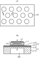
- FIG. 4A and 4B are sectional views of the diaphragm when the piezoelectric element according to the embodiment of the present invention is applied to the diaphragm.
- 4A is a top view of the diaphragm
- FIG. 4B is a cross-sectional view taken along the line BB in FIG. 4A.
- the diaphragm includes a plurality of diaphragm elements DE arranged in a staggered manner in a necessary region on the upper surface of the lower electrode layer L21.
- the diaphragm element DE has a cylindrical shape, and has a stress relaxation layer L22 formed in the lower layer, a piezoelectric layer L3 formed in the middle layer, and a size slightly larger than the size of the upper surface of the piezoelectric layer L3. And an upper electrode layer L4.
- the size of the cross section of the removal portion RD is, for example, the same size as the cross section of the diaphragm element DE.
- each diaphragm element DE is connected to an external control circuit by, for example, an unillustrated wiring.
- the designated diaphragm element DE can be driven by applying an electrical signal from the control circuit to the designated diaphragm element DE.
- the piezoelectric layer L3 expands and contracts in the left-right direction, and the substrate L11 above the removal portion RD, heat
- the oxide film L12, the lower electrode layer L21, and the diaphragm element DE are bent up and down.
- this diaphragm can be used as a pump by attaching a plate with holes formed on the lower surface of the removal portion RD and filling the removal portion RD with gas or liquid. Moreover, this diaphragm can be used as a printer head of an inkjet printer by filling the removal part RD with ink.
- the diaphragm when the diaphragm is vibrated by sound waves or ultrasonic waves, an electric field is generated between the upper electrode layer L4 and the lower electrode layer L21 due to an effect opposite to the above, and charges are accumulated in both electrode layers. Therefore, the amount of deformation of the diaphragm can be detected by detecting the amount of charge accumulated in both electrode layers.
- the diaphragm can be used as a sensor by detecting the frequency and amplitude of the diaphragm.
- FIG. 5 is a view showing a modification of the piezoelectric element according to the embodiment of the present invention.
- the lower electrode layer L21 is formed over the entire upper surface of the thermal oxide film L12.
- the lower electrode layer L21 is the same size or slightly larger than the lower surface of the stress relaxation layer L22. It is formed.
- Such a lower electrode layer L21 is formed by, for example, forming the lower electrode layer L21 over the entire upper surface of the thermal oxide film L12 by sputtering, then protecting the remaining region of the lower electrode layer L21 with a resist agent, and then etching the lower electrode layer L21. Therefore, the lower electrode layer L21 that is not necessary may be removed.
- the stress relaxation layer L22 made of MgO may be formed after removing the unnecessary region of the lower electrode layer L21. As a result, the area of the lower electrode layer L21 is reduced, the stress relaxation layer L22 made of MgO formed on the upper surface of the lower electrode layer L21 can also be better single-crystallized, and the piezoelectric layer L3 can be more easily single-crystallized. It can be crystallized.
- the intermediate layer L2 is composed of the lower electrode layer L21 and the stress relaxation layer L22.
- the stress relaxation layer L22 may be omitted.
- the lattice constant of the lower electrode layer L21 is closer to the lattice constant of the piezoelectric layer L3 than the lattice constant of the thermal oxide film L12. Therefore, compared to the case where the piezoelectric layer L3 is formed directly on the thermal oxide film L12, the piezoelectric layer L3 is better formed as a single crystal when the piezoelectric layer L3 is formed on the thermal oxide film L12 via the lower electrode layer L21. It can be made.
- the stress relaxation layer L22 Since the lattice constant of the stress relaxation layer L22 is closer to the lattice constant of the piezoelectric layer L3 than the lattice constant of the lower electrode layer L21, the stress relaxation layer is compared with the case where the piezoelectric layer L3 is formed on the lower electrode layer L21. When the piezoelectric layer L3 is formed via L22, the piezoelectric layer L3 can be single-crystallized better.
- PZT is adopted as the piezoelectric layer L3.
- relaxor materials such as PMN (lead magnesium niobate) and PZN (lead zinc niobate) may be adopted.
- the stress relaxation layer L22 in the region where the piezoelectric layer L3 is not formed is removed in advance, and the region where the piezoelectric layer L3 is formed is reduced.
- the stress on the piezoelectric layer L3 due to the difference in lattice constant from the piezoelectric layer L3 and thermal expansion is alleviated, and the piezoelectric layer L3 can be well single crystallized.
- a method of manufacturing a piezoelectric element includes a first step of forming an intermediate layer on a top surface of a substrate layer for relieving stress applied to the piezoelectric layer when the piezoelectric layer is formed, A second step of removing a part of the intermediate layer leaving a region where the piezoelectric layer is to be formed; and a third step of forming the piezoelectric layer on the upper surface of the intermediate layer.
- the piezoelectric layer is formed on the upper surface of the remaining intermediate layer after a part of the intermediate layer is removed leaving a region where the piezoelectric layer is formed.
- the intermediate layer in the region where the piezoelectric layer is not formed is removed in advance and the region where the piezoelectric layer is formed is reduced, the difference in lattice constant between the intermediate layer and the piezoelectric layer and the piezoelectric layer due to thermal expansion are reduced. The stress is relaxed, and the piezoelectric layer can be satisfactorily single-crystallized.
- the second step preferably removes the periphery of the intermediate layer while leaving a predetermined independent region.
- the intermediate layer is formed in an island shape on the upper surface of the substrate, and the piezoelectric layer can be formed at the center of the upper surface of the substrate. Therefore, the vibration of the piezoelectric layer can be evenly transmitted to the substrate, and a good piezoelectric element can be manufactured as an ink head or the like of an ink jet printer.
- the intermediate layer includes an electrode layer and a stress relaxation layer.
- the electrode layer is formed on the upper surface of the substrate layer, and the stress relaxation layer is formed on the upper surface of the formed electrode layer. It is preferable.
- the piezoelectric element in which the electrode layer and the stress relaxation layer are laminated on the upper surface of the substrate layer.
- the intermediate layer includes not only the electrode layer but also the stress relaxation layer, the stress generated when the piezoelectric layer is formed on the upper surface of the stress relaxation layer can be more reliably relaxed, and the piezoelectric layer can be made into a single crystal more reliably. can do.
- the piezoelectric layer is formed on the upper surface of the electrode layer and the upper surface of the stress relaxation layer. It is preferable to form a layer and remove the piezoelectric layer formed on the upper surface of the electrode layer.
- the substrate layer includes a substrate and a thermal oxide film, and in the first step, the intermediate layer is formed on an upper surface of the thermal oxide film.
- the intermediate layer and the substrate can be insulated and both can be protected.
- a piezoelectric element includes a substrate layer and a region where the piezoelectric layer is to be formed on the upper surface of the substrate layer in order to relieve stress applied to the piezoelectric layer when the piezoelectric layer is formed.
- An intermediate layer formed so as to remove a part of the region excluding, and a piezoelectric layer formed on the upper surface of the intermediate layer.
- the intermediate layer is formed only in the region where the piezoelectric layer is formed, the region where the piezoelectric layer is formed is reduced, and the stress generated in the piezoelectric layer is reduced when the piezoelectric layer is formed.
- the substrate layer has an oxide film layer formed on a surface thereof, and the intermediate layer has a lower electrode layer formed on an upper surface of the oxide film layer and a predetermined upper surface of the lower electrode layer.
- the piezoelectric layer is formed on an upper surface of the stress relaxation layer, and further includes an upper electrode layer formed on the upper surface of the stress relaxation layer.
- the lattice constant preferably has a value between the lattice constant of the lower electrode layer and the lattice constant of the piezoelectric layer.
- the intermediate layer includes the lower electrode layer and the stress relaxation layer
- the lattice constant of the stress relaxation layer has a value between the lattice constant of the lower electrode layer and the lattice constant of the piezoelectric layer.
Landscapes
- Engineering & Computer Science (AREA)
- Manufacturing & Machinery (AREA)
- Chemical & Material Sciences (AREA)
- Combustion & Propulsion (AREA)
- Mechanical Engineering (AREA)
- General Engineering & Computer Science (AREA)
- Particle Formation And Scattering Control In Inkjet Printers (AREA)
Abstract
基板層L1の上面に圧電層L3の応力緩和するためのMgOからなる応力緩和層L22を形成し、圧電層L3が形成される領域D1を残して応力緩和層L22を除去し、応力緩和層L22の上面に単結晶の圧電層L3を形成する。これにより、圧電層L3が形成されない領域D2の応力緩和層L22が予め除去され、圧電層L3が形成される領域D1が縮小化され、応力緩和層L22と圧電層L3との格子定数の差や熱膨張による圧電層L3への応力が緩和され、圧電層L3を良好に単結晶化させることができる。
Description
本発明は、単結晶の圧電層を含む圧電素子に関するものである。
従来から、駆動素子やセンサなどの機械電気変換素子として、チタン酸ジルコンサン鉛(PZT)等から構成される圧電体が用いられている。また、近年、装置の小型化、高密度化、及び低コスト化などの要求に応えるために、シリコン基板を用いたMEMS(Micro Electro Mechanical Systems)による機械電気変換素子が増加している。
機械電気変換素子をMEMSで構成するには、圧電体を薄膜化することが望ましい。これにより、成膜及びフォトリソグラフィー等の半導体プロセス技術を用いた高精度な加工が可能となり、機械電気変換素子を小型化及び高密度化することができる。また、機械電気変換素子をMEMSで構成すると、大面積のウェハを用いて複数の機械電気変換素子を一括加工できるため、コストを低減することができる。更に、機械電気変換素子の変換効率が向上し、駆動素子の特性やセンサの感度を向上させることができる。
PZT等の圧電体をシリコン(Si)等の基板上に成膜する手法として、CVD法等の化学的な手法、スパッタ法やイオンプレーティング法等の物理的な手法、及びゾルゲル法等の液相を用いて圧電体を成長させる手法が知られている。
PZT等の圧電体は、その結晶構造がペロブスカイト型構造をとるときに良好な圧電効果を実現することができる。図6は、ペロブスカイト構造をとるPZTの結晶構造を示した図である。図6に示すように、PZTは、チタン酸鉛とジルコン酸鉛との混晶からなり、立方体の中心にチタン(Ti)又はジルコン(Zr)が配置され、各頂点に鉛(Pb)が配置され、各面の中心に酸素が配置されたペロブスカイト構造を有していることが分かる。
また、ペロブスカイト構造をとる圧電体の薄膜においては、薄膜が均一な単結晶構造をとるときに大きな圧電特性を得ることができる。
この傾向はPZTのジルコン(Zr)、チタン(Ti)を他の元素で置き換えたPMN(マグネシウムニオブ酸鉛),PZN(亜鉛ニオブ酸鉛)等のいわゆるリラクサ材料と呼ばれる物質で顕著であることが知られている(非特許文献1のP29の図4)。
ところが、PZT等の圧電体とSiとは格子定数が異なるため、Si基板上に圧電体を成膜すると、図7に示すように、圧電体は方位の異なる複数の結晶が柱状に寄り集まった多結晶構造となる(非特許文献1のP133の図9)。図7は、基板の上面にPZTからなる圧電体を形成したときの圧電体の断面図である。図7に示す圧電体では、1つの領域は結晶方位が揃っているが、隣接する領域同士は結晶方位が異なっており、圧電体が多結晶構造を有している。多結晶構造では結晶粒界で変位の拘束が生じ、この影響により単結晶構造に比べて圧電特性が低下する。また、多結晶構造では結晶粒界による電流リークにより大きな電界を印加できないという課題もある。
このような課題を解決するために下記の技術が知られている。特許文献1では、圧電体とSi基板との格子定数の不整合を緩和するために、両者の間にMgO等からなる緩和層を設ける技術が開示されている。
また、特許文献2では、基板上にスパッタリングにより強誘電体薄膜を形成する手法において、基板の外形を短冊状にすることで、スパッタリング後の冷却に際し、基板の長辺と短辺との引っ張り応力又は圧縮応力に顕著な差を生じさせ、強誘電体薄膜を単結晶化する技術が開示されている。
また、特許文献3では、基板上に2枚の下部電極を形成し、その上に圧電体を成膜し、これら2枚の下部電極及び圧電体が基板上で柱状に複数個形成されるように、これら2枚の下部電極及び圧電体の不要な領域を除去した後、加熱処理することにより圧電体を単結晶化する技術が開示されている。
しかしながら、特許文献1においては、圧電体とSi基板との間に緩和層が設けられているが、圧電体とSi基板との格子定数の差が大きいため、圧電体を広範囲に形成すると、圧電体が単結晶化されないという問題がある。
また、特許文献2においては、基板と強誘電体薄膜との間に緩和層が設けられておらず、両者の格子定数の不整合が大きいため、強誘電体薄膜を単結晶化するには限界がある。
また、特許文献3においては、熱処理により圧電体が単結晶化されているが、下部電極と圧電体との間に両者の格子定数を緩和するための緩和層が設けられていないため、圧電体を単結晶化するにも一定の限界がある。つまり、成膜後の加熱処理では原子の移動範囲に限界があるため、圧電体の結晶方位のばらつきが大きい場合は、熱処理したとしても圧電体を単結晶化することは困難である。
文献名:圧電材料の高性能化と先端応用技術、発行元:サイエンス&テクノロジー株式会社
本発明の目的は、圧電層を良好に単結晶化することができる圧電素子の製造方法及びその製造方法により製造された圧電素子を提供することである。
本発明の一局面による圧電素子の製造方法は、基板層の上面に、圧電層の成膜時に前記圧電層に加わる応力を緩和するための中間層を形成する第1ステップと、前記圧電層が形成されるべき領域を残して前記中間層の一部を除去する第2ステップと、前記中間層の上面に前記圧電層を形成する第3ステップとを備えている。
また、本発明の別の一局面による圧電素子は、基板層と、圧電層の成膜時に前記圧電層に加わる応力を緩和するために前記基板層の上面において、前記圧電層が形成されるべき領域を除く一部の領域が除去されるように形成された中間層と、前記中間層の上面に形成された圧電層とを備えている。
図1(A)~(E)は、本発明の実施の形態による圧電素子が製造される様子を示した圧電素子の構造図であり、(A)~(E)へとアルファベットの順序が進につれて、製造工程が進行している。
図1(E)に示すように圧電素子は、基板層L1、基板層L1の上面に形成され、圧電層L3の成膜時に圧電層L3に加わる応力を緩和するための中間層L2、中間層L2の上面に形成された圧電層L3、及び圧電層L3の上面に形成された上部電極層L4を備えている。
基板層L1は、基板L11及び基板L11の上面に形成された熱酸化膜L12を含んでいる。基板L11は、例えばシリコンにより構成されている。基板L11の厚みt11としては、製造されるデバイスにより異なるが、例えば300μm~500μm程度を採用することができる。
熱酸化膜L12は、基板L11を保護及び絶縁することを目的として基板L11の上面に形成され、基板L11を例えば1500℃程度で加熱することで形成されたSiO2により構成されている。熱酸化膜L12の厚みt12としては、例えば0.1μm程度を採用することができる。
中間層L2は、熱酸化膜L12の上面に形成された下部電極層L21、及び下部電極層L21の上面に形成された応力緩和層L22を含んでいる。
下部電極層L21は、熱酸化膜L12の上面に形成されたチタン(Ti)と、チタンの上面に形成された白金(Pt)とを含んでいる。チタンは、熱酸化膜L12と白金との密着性を向上させるために設けられ、例えば0.02μm程度の膜厚を備えている。また、白金の膜厚としては、例えば0.1μm程度が採用されている。したがって、下部電極層L21の膜厚t21としては、例えば0.12μm程度を採用することができる。なお、下部電極層L21は、例えばスパッタ法を用いて、チタン、白金の順で形成される。
応力緩和層L22は、例えば酸化マグネシウム(MgO)により構成され、下部電極層L21の白金の上面に形成されている。ここで、応力緩和層L22の格子定数は、下部電極層L21の格子定数と圧電層L3の格子定数との間の値を持ち、かつ、下部電極層L21の格子定数よりも圧電層L3の格子定数に近い。そのため、応力緩和層L22が存在することで、圧電層L3の単結晶成長を促進させることができる。つまり、下部電極層L21の上層を構成する白金と圧電層L3との格子定数の差に起因して圧電層L3の成膜時に圧電層L3に発生する応力が緩和され、圧電層L3をより良好に単結晶化させることができる。
また、応力緩和層L22は、例えばスパッタ法により形成され、その膜厚t22は例えば0.01μm程度である。また、応力緩和層L22は、圧電層L3が形成されるべき領域D1のみ残され、圧電層L3が形成されない領域D2は除去される。
また、圧電層L3は円柱形状を有している。こうすることで、成膜時に圧電層L3への応力が対称的に加わり、圧電層L3をより良好に単結晶化することができる。また、圧電層L3の膜厚t3としては、用途によっても異なるが、メモリやセンサでは例えば1μm以下程度の値が採用され、アクチュエータでは5μm以下程度の値が採用される。
また、圧電層L3が形成される領域D1にのみ応力緩和層L22が存在し、圧電層L3が形成されない領域D2には応力緩和層L22が存在しない。そのため、圧電層L3が形成される領域が縮小化され、応力緩和層L22と圧電層L3との格子定数の差や熱膨張による圧電層L3への応力が緩和され、圧電層L3を良好に単結晶化させることができる。
応力緩和層L22と圧電層L3との格子定数の差は小さいため、図1(C)に示すように、領域D1においては、圧電層L3は単結晶で成長する。一方、下部電極層L21の白金と圧電層L3との格子定数の差は、応力緩和層L22と圧電層L3との格子定数の差に比べて大きいため、図1(C)に示すように、領域D2においては、圧電層L3は多結晶で成長する可能性が高い。
上部電極層L4は、下層に形成されたチタンと、上層に形成された白金とを含む。上部電極層L4を構成するチタン及び白金の膜厚としては、下部電極層L21を構成するチタン及び白金と同程度の値を採用すればよい。
図1(A)~(E)を用いて圧電素子の製造方法を簡単に説明すると下記のようになる。すなわち、図1(A)では、基板L11上に熱酸化膜L12と下部電極層L21とがそれぞれ、この順で、基板L11の上面の全域に形成される。
図1(B)では、圧電層L3が形成される下部電極層L21の一部の領域D1に応力緩和層L22が形成される。
図1(C)では、圧電層L3が下部電極層L21の上面及び応力緩和層L22の上面、すなわち、基板L11の上面の全域に形成される。そして、領域D1に形成された圧電層L31は単結晶となり、領域D2に形成された圧電層L32は多結晶となっている。
図1(D)では,下層にチタン、上層に白金からなる上部電極層L4が圧電層L3の上面に形成される。
図1(E)では、圧電層L32が除去され、圧電層L31のみが残され、圧電素子が完成する。
次に、本実施の形態による圧電素子の製造方法について具体的に説明する。図2は、本発明の実施の形態による圧電素子の製造方法に用いられるスパッタ装置の概要を示す断面図である。
このスパッタ装置は高周波マグネトロンスパッタ法により圧電体等の薄膜を成膜する装置であり、ターゲット1、ターゲット皿2、マグネット3、カバー4、高周波電極5、絶縁体6、真空チャンバー7、高周波電源8、基板9(L11)、基板加熱ヒーター10、バルブ12,13、及びスパッタガスを真空チャンバー7内に供給するノズル14等を備えている。
真空チャンバー7は、断面形状が四角形状の箱体により構成され、底壁の中央には、高周波電極5とマグネット3とが埋設されている。マグネット3は上面が真空チャンバー7の底壁の上面と連なっている。また、高周波電極5はマグネット3の下側に配設されている。真空チャンバー7の底壁であってマグネット3の上側にはターゲット皿2が載置される。
ターゲット皿2は、ターゲット1が充填され、マグネット3の上側に載置される。カバー4は、ターゲット1の表面の原子を基板9に飛翔させるべく、上側が開放されており、ターゲット皿2を取り囲むように、真空チャンバー7の底壁に立設されている。また、高周波電極5は、高周波電源8が接続され、高周波電力が印加されることで、真空チャンバー7内にマイクロ波を発生させる。高周波電源8は、一端が高周波電極5に接続され、他端が接地されている。
真空チャンバー7の一方の壁面には2分岐したノズル14が設けられている。ノズル14の一方の分岐路にはアルゴン(Ar)が供給され、他方の分岐路には酸素(O2)が供給され、アルゴン及び酸素からなるスパッタガスが真空チャンバー7内に供給される。真空チャンバー7内に供給されたスパッタガスは、真空チャンバー7内に発生したマイクロ波によってブラズマ化される。また、ノズル14のそれぞれの分岐路にはバルブ12,13が取り付けられ、Ar及びO2の流量が調整される。
真空チャンバー7の他方の側面には、排気口15が設けられている。この排気口15には真空チャンバー7内のガスを排気するための例えばバルブ及びポンプ(図略)が接続されている。
真空チャンバー7の上壁には、棒状の支持部材がターゲット1に向けて設けられている。基板加熱ヒーター10は、この支持部材によってターゲット1と対向するように真空チャンバー7の上壁から吊されている。ここで、基板加熱ヒーター10は、例えば、直方体形状を有する導電性の部材からなる筐体により覆われている。基板9は、基板加熱ヒーター10の筐体の下面に当接するように真空チャンバー7内に設置され、基板加熱ヒーター10によって加熱される。マグネット3と高周波電極5とは、絶縁体6によって真空チャンバー7から絶縁されている。
なお、基板加熱ヒーター10、高周波電源8、及びバルブ12,13は、制御装置(図略)と接続されている。また、真空チャンバー7には、真空チャンバー7内の温度を測定するための温度センサと、真空チャンバー7内の圧力を測定するための圧力センサとが設けられている。
そして、制御装置は、温度センサによる測定データに基づいて、基板加熱ヒーター10の発熱量を調整し、真空チャンバー7内の温度調節を行う。また、制御装置は、圧力センサによる測定データに基づいて、バルブ12,13の開度、並びに排気口15側に設けられた図略のバルブの開度及びポンプの稼働を制御し、真空チャンバー7内の圧力を調整する。
また、制御装置は、高周波電源8をオン、オフさせ、真空チャンバー7内にマイクロ波を発生させたり、マイクロ波の発生を停止させたりする。
図2に示すスパッタ装置では、所定の組成比に調合したPZT材料の粉末を混合、焼成、及び粉砕し、ターゲット皿2に充填してプレス機で加圧することによりターゲット1を作製する。このターゲット1が載せられたターゲット皿2をマグネット3上に設置し、ターゲット皿2を取り囲むようにカバー4を設置する。そして、基板9を,基板加熱ヒーター10の筐体の下面に設置する。そして、真空チャンバー7内の空気を排気し、基板加熱ヒーター10によって基板9を例えば600℃にまで加熱する。
そして、基板9の加熱後、バルブ12及び13を開け、スパッタガスであるArとO2を所定の割合でノズル14を介して真空チャンバー7内に導入し、真空度を所定値に保つ。そして、高周波電源8を駆動させ、高周波電極5からマイクロ波を発生させてスパッタガスをプラズマ化し、基板9上にPZTからなる圧電層L3を成膜する。
図3は、本発明の実施の形態による圧電素子の製造方法を示すフローチャートである。まず、基板L11が例えば1500℃程度で加熱され、基板L11の上面にSiO2からなる熱酸化膜L12が形成される(ステップS1)。
次に、チタンのターゲット1を作製し、熱酸化膜L12が形成された基板L11をスパッタ装置に設置し、スパッタ法により熱酸化膜L12の上面の全域にチタンが成膜される(ステップS2)。次に、ターゲット1として白金が採用され、チタンと同様にしてスパッタ法によりチタンの上面の全域に白金が成膜される(ステップS3)。ステップS2,S3の処理により、図1(A)に示すように熱酸化膜L12の上面の全域に下部電極層L21が形成される。
次に、ターゲット1としてMgOが採用され、スパッタ法により下部電極層L21の上面の全域にMgOからなる応力緩和層L22が成膜される(ステップS4)。
次に、応力緩和層L22の上面の全域にレジスト剤がスピンコート法により塗布される(ステップS5)。次に、レジスト剤が乾燥され、応力緩和層L22の上面の領域D1のみにレジスト剤を残存させるべく、マスクを介してレジスト剤が露光及び現像される(ステップS6)。これにより、領域D1の応力緩和層L22が保護される。
次に、レジスト剤が塗布された基板L11をエッチング溶液に浸漬し、領域D2の応力緩和層L22が除去される(ステップS7)。ここで、エッチング溶液としては、例えばフッ酸と硝酸との混合液を用いることができる。これにより、図1(B)に示すように、領域D1のみ応力緩和層L22が残存する基板L11が得られる。
次に、PZT材料の粉末を用いてターゲット1を作製し、領域D2の応力緩和層L22が除去された中間生成物をスパッタ装置に設置し、スパッタ法により下部電極層L21の上面及び応力緩和層L22の上面に圧電層L3を成膜する(ステップS8)。
次に、圧電層L3の上面の全域にレジスト剤がスピンコート法により塗布される(ステップS9)。次に、必要となる圧電層L31の上面の全域よりも多少小さな領域にのみレジスト剤を除去させるべく、マスクパターンを介してレジスト剤が露光及び現像される(ステップS10)。これにより、上部電極層L4が形成される領域以外の圧電層L3がレジスト剤により保護される。
ここで、上部電極層L4が形成される領域は、領域D1の上面の圧電層L31の領域よりも多少小さなサイズにされている。これにより上部電極層L4と下部電極層L21との導通を防止することができる。
次に、圧電層L3の上面の全域に蒸着法によりチタンが成膜される(ステップS11)。次に、成膜されたチタンの上面の全域に蒸着法を用いて白金が成膜される(ステップS12)。
次に、白金が成膜された基板L11がエッチング溶液に浸漬され、チタン及び白金がレジスト剤と共に剥離されるリフトオフが行われる(ステップS13)。これにより、図1(D)に示すように、必要となる圧電層L31の上面の全域よりも多少小さな領域に、下層にチタン、上層に白金からなる上部電極層L4が形成される。ここで、エッチング溶液としては、レジスト剤が指定するものを用いればよい。
次に、上部電極層L4が形成された圧電層L3の上面の全域にレジスト剤がスピンコート法により塗布される(ステップS14)。次に、領域D1の上面の圧電層L31のみにレジスト剤を残存するべく、マスクパターンを介してレジスト剤が露光及び現像される(ステップS15)。これにより、領域D1の上面の圧電層L31がレジスト剤によって保護される。
次に、ステップS15により得られた基板L11がエッチング溶液に浸漬され、領域D2の上側の不要な圧電層L32が除去される(ステップS16)。ここで、エッチング溶液としては応力緩和層L22を除去する場合に用いたエッチング溶液と同様、フッ酸と硝酸との混合液からなるエッチング溶液を用いればよい。これにより、図1(E)に示す圧電素子が得られる。
なお、図3において、ステップS1~S4が、基板層L1の上面に圧電層L3の成膜時に圧電層L3に加わる応力を緩和するための中間層を形成する第1ステップの一例に相当する。また、ステップS5~S7が、圧電層L3が形成されるべき領域D1を残して中間層L2の一部を除去する第2ステップの一例に相当する。また、ステップS8~S16が、中間層L2の上面に単結晶の圧電層L3を形成する第3ステップの一例に相当する。
次に、上記の製造方法を経て得られた圧電素子をダイヤフラムに応用した場合について説明する。図4(A)、(B)は本発明の実施の形態による圧電素子をダイヤフラムに応用した場合のダイヤフラムの断面図である。図4(A)は、ダイヤフラムの上面図を示し、図4(B)は、図4(A)のB-B断面図を示している。
図4(A)に示すように、ダイヤフラムは、下部電極層L21の上面の必要な領域において千鳥状に配設された複数のダイヤフラムエレメントDEを備えている。ダイヤフラムエレメントDEは円柱形状を有し、下層に形成された応力緩和層L22と、中層に形成された圧電層L3と、上層に形成され、圧電層L3の上面のサイズよりも多少小さなサイズを有する上部電極層L4とを備えている。
図4(B)に示すように、ダイヤフラムエレメントDEが形成されている領域では、基板L11の一部が円柱状に除去されて除去部RDが形成されている。ここで、除去部RDの断面のサイズはダイヤフラムエレメントDEの断面と例えば同一サイズである。
各ダイヤフラムエレメントDEを構成する上部電極層L4と下部電極層L21とは、例えば図略の配線により外部の制御回路と接続されている。そして、この制御回路から、指定のダイヤフラムエレメントDEに電気信号を印加することにより、指定のダイヤフラムエレメントDEを駆動させることができる。
指定したダイヤフラムエレメントDEに係る下部電極層L21と上部電極層L4とに所定の電界を加えると、圧電層L3が左右方向に伸縮し、バイメタルの原理により、除去部RDの上部の基板L11、熱酸化膜L12、下部電極層L21、及びダイヤフラムエレメントDEが上下に湾曲する。
したがって、除去部RDの下面に孔が形成された板を取り付け、除去部RD内に気体や液体を充填するとで、このダイヤフラムをポンプとして用いることができる。また、除去部RDにインクを充填することで、このダイヤフラムをインクジェットプリンタのプリンタヘッドとして用いることができる。
また、音波や超音波によりダイヤフラムが振動すると、上記と反対の効果により上部電極層L4及び下部電極層L21間に電界が発生し、両電極層に電荷が蓄積される。したがって、両電極層に蓄積された電荷量を検出することにより、ダイヤフラムの変形量を検出することができる。そして、ダイヤフラムの周波数や振幅等を検出することにより、このダイヤフラムをセンサとして用いることができる。
図5は、本発明の実施の形態による圧電素子の変形例を示した図である。図1(E)では、下部電極層L21は、熱酸化膜L12の上面の全域に形成されているが、図5では、下部電極層L21は、応力緩和層L22の下面と同一又は多少大きなサイズを有して形成されている。
このような下部電極層L21は、例えば、熱酸化膜L12の上面の全域にスパッタ法で下部電極層L21を成膜した後、残存させる下部電極層L21の領域をレジスト剤で保護した後、エッチングにより不要となる下部電極層L21を除去すればよい。
なお、MgOからなる応力緩和層L22の成膜は、下部電極層L21の不要となる領域の除去後に実施すればよい。これにより、下部電極層L21の面積が小さくなり、下部電極層L21の上面に形成されるMgOからなる応力緩和層L22もより良好に単結晶化することができ、圧電層L3をより良好に単結晶化させることができる。
また、図1(E)及び図5に示す圧電素子では、中間層L2を下部電極層L21及び応力緩和層L22から構成したが、応力緩和層L22を省いても良い。下部電極層L21の格子定数は熱酸化膜L12の格子定数よりも圧電層L3の格子定数に近い。そのため、熱酸化膜L12に直接、圧電層L3を形成する場合に比べて、熱酸化膜L12に下部電極層L21を介して圧電層L3を形成した方が、圧電層L3をより良好に単結晶化させることができる。
なお、応力緩和層L22の格子定数は、下部電極層L21の格子定数よりも圧電層L3の格子定数に近いため、下部電極層L21の上に圧電層L3を形成する場合に比べて応力緩和層L22を介して圧電層L3を形成する方が、圧電層L3をより良好に単結晶化することができる。
また、上記説明では、圧電層L3としてPZTを採用したが、これに限定されず、PMN(マグネシウムニオブ酸鉛)及びPZN(亜鉛ニオブ酸鉛)等のリラクサ材料を採用してもよい。
以上説明したように、上記の圧電素子は、圧電層L3が形成されない領域の応力緩和層L22を予め除去し、圧電層L3が形成される領域を縮小化させているため、応力緩和層L22と圧電層L3との格子定数の差や熱膨張による圧電層L3への応力が緩和され、圧電層L3を良好に単結晶化させることができる。
上記圧電素子の製造方法及び圧電素子の技術的特徴をまとめると下記のようになる。
(1)本発明の一局面による圧電素子の製造方法は、基板層の上面に、圧電層の成膜時に前記圧電層に加わる応力を緩和するための中間層を形成する第1ステップと、前記圧電層が形成されるべき領域を残して前記中間層の一部を除去する第2ステップと、前記中間層の上面に前記圧電層を形成する第3ステップとを備えている。
この構成によれば、圧電層が形成される領域を残して中間層の一部が除去された後、残存する中間層の上面に圧電層が形成されている。つまり、圧電層が形成されない領域の中間層を予め除去し、圧電層が形成される領域を縮小化させているため、中間層と圧電層との格子定数の差や熱膨張による圧電層への応力が緩和され、圧電層を良好に単結晶化させることができる。
(2)前記第2ステップは、前記中間層上の所定の独立した領域を残して、その周囲を除去することが好ましい。
この構成によれば、基板の上面に島状に中間層が形成され、圧電層を基板の上面の中央部に形成することができる。そのため、圧電層の振動を基板に対して均等に伝達することができ、インクジェットプリンタのインクヘッド等として良好な圧電素子を製造することができる。
(3)前記中間層は、電極層及び応力緩和層を含み、前記第1ステップは、前記基板層の上面に前記電極層を形成し、形成した電極層の上面に前記応力緩和層を形成することが好ましい。
この構成によれば、基板層の上面に電極層及び応力緩和層が積層された圧電素子を提供することができる。また、中間層が電極層のみならず応力緩和層も含んでいるため、応力緩和層の上面に圧電層を形成する際に生じる応力をより確実に緩和させ、圧電層をより確実に単結晶化することができる。
(4)前記第2ステップは、前記電極層の上面に形成された前記応力緩和層の一部を除去し、前記第3ステップは、前記電極層の上面及び前記応力緩和層の上面に前記圧電層を形成し、前記電極層の上面に形成された圧電層を除去することが好ましい。
この構成によれば、応力緩和層の上面に形成され、良好に単結晶化された圧電層のみが残され、電極層の上面に形成され、単結晶化されていない圧電層が除去されているため、良好に単結晶化された圧電層を有する圧電素子を製造することができる。
(5)前記基板層は、基板及び熱酸化膜を含み、前記第1ステップは、前記熱酸化膜の上面に前記中間層を形成することが好ましい。
この構成によれば、中間層と基板との間に熱酸化膜が形成されているため、中間層と基板とを絶縁し、両者を保護することができる。
(6)本発明の一局面による圧電素子は、基板層と、圧電層の成膜時に前記圧電層に加わる応力を緩和するために前記基板層の上面において、前記圧電層が形成されるべき領域を除く一部の領域が除去されるように形成された中間層と、前記中間層の上面に形成された圧電層とを備えている。
この構成によれば、圧電層が形成される領域にのみ中間層が形成されているため、圧電層が形成される領域が縮小化され、圧電層を形成する際に圧電層に生じる応力が緩和され、良好に単結晶化された圧電層を持つ圧電素子を提供することができる。
(7)上記圧電素子において、前記基板層は、表面に酸化膜層が形成され、前記中間層は、前記酸化膜層の上面に形成された下部電極層と、前記下部電極層の上面の所定の領域に形成された応力緩和層とを含み、前記圧電層は、前記応力緩和層の上面に形成され、前記応力緩和層の上面に形成された上部電極層を更に備え、前記応力緩和層の格子定数は、前記下部電極層の格子定数と前記圧電層の格子定数との間の値を持つことが好ましい。
この構成によれば、中間層に下部電極層と応力緩和層とが含まれ、応力緩和層の格子定数が下部電極層の格子定数と圧電層の格子定数との間の値を持っている。これにより、圧電層の格子定数は、下部電極層の格子定数よりも応力緩和層の格子定数に近くなり、圧電層を下部電極層の上面に直接形成する場合に比べて、圧電層の形成時に圧電層に生じる応力をより確実に緩和することができる。その結果、圧電層をより良好に単結晶化させることができる。
Claims (7)
- 基板層の上面に、圧電層の成膜時に前記圧電層に加わる応力を緩和するための中間層を形成する第1ステップと、
前記圧電層が形成されるべき領域を残して前記中間層の一部を除去する第2ステップと、
前記中間層の上面に前記圧電層を形成する第3ステップとを備える圧電素子の製造方法。 - 前記第2ステップは、前記中間層上の所定の独立した領域を残して、その周囲を除去する請求項1記載の圧電素子の製造方法。
- 前記中間層は、電極層及び応力緩和層を含み、
前記第1ステップは、前記基板層の上面に前記電極層を形成し、形成した電極層の上面に前記応力緩和層を形成する請求項1記載の圧電素子の製造方法。 - 前記第2ステップは、前記電極層の上面に形成された前記応力緩和層の一部を除去し、
前記第3ステップは、前記電極層の上面及び前記応力緩和層の上面に前記圧電層を形成し、前記電極層の上面に形成された圧電層を除去する請求項3記載の圧電素子の製造方法。 - 前記基板層は、基板及び熱酸化膜を含み、
前記第1ステップは、前記熱酸化膜の上面に前記中間層を形成する請求項1記載の圧電素子の製造方法。 - 基板層と、
圧電層の成膜時に前記圧電層に加わる応力を緩和するために前記基板層の上面において、前記圧電層が形成されるべき領域を除く一部の領域が除去されるように形成された中間層と、
前記中間層の上面に形成された圧電層とを備える圧電素子。 - 前記基板層は、表面に酸化膜層が形成され、
前記中間層は、前記酸化膜層の上面に形成された下部電極層と、前記下部電極層の上面の所定の領域に形成された応力緩和層とを含み、
前記圧電層は、前記応力緩和層の上面に形成され、
前記応力緩和層の上面に形成された上部電極層を更に備え、
前記応力緩和層の格子定数は、前記下部電極層の格子定数と前記圧電層の格子定数との間の値を持つ請求項6記載の圧電素子。
Priority Applications (3)
| Application Number | Priority Date | Filing Date | Title |
|---|---|---|---|
| EP10843004.2A EP2525423B1 (en) | 2010-01-12 | 2010-12-21 | Method for manufacturing piezoelectric element, and piezoelectric element manufactured by the method |
| JP2011549772A JP5549680B2 (ja) | 2010-01-12 | 2010-12-21 | 圧電素子の製造方法及びその製造方法により製造された圧電素子 |
| US13/521,955 US9157378B2 (en) | 2010-01-12 | 2010-12-21 | Method for manufacturing piezoelectric element and piezoelectric element manufactured using same |
Applications Claiming Priority (2)
| Application Number | Priority Date | Filing Date | Title |
|---|---|---|---|
| JP2010-004277 | 2010-01-12 | ||
| JP2010004277 | 2010-01-12 |
Publications (1)
| Publication Number | Publication Date |
|---|---|
| WO2011086645A1 true WO2011086645A1 (ja) | 2011-07-21 |
Family
ID=44303951
Family Applications (1)
| Application Number | Title | Priority Date | Filing Date |
|---|---|---|---|
| PCT/JP2010/007389 Ceased WO2011086645A1 (ja) | 2010-01-12 | 2010-12-21 | 圧電素子の製造方法及びその製造方法により製造された圧電素子 |
Country Status (4)
| Country | Link |
|---|---|
| US (1) | US9157378B2 (ja) |
| EP (1) | EP2525423B1 (ja) |
| JP (1) | JP5549680B2 (ja) |
| WO (1) | WO2011086645A1 (ja) |
Cited By (4)
| Publication number | Priority date | Publication date | Assignee | Title |
|---|---|---|---|---|
| JP2013110180A (ja) * | 2011-11-18 | 2013-06-06 | Konica Minolta Holdings Inc | 圧電素子およびその製造方法 |
| JP2017162906A (ja) * | 2016-03-08 | 2017-09-14 | 富士フイルム株式会社 | 圧電素子 |
| US20220199114A1 (en) * | 2013-03-18 | 2022-06-23 | Magnecomp Corporation | Multi-Layer PZT Microactuator with Active PZT Constraining Layers for a DSA Suspension |
| CN117460388A (zh) * | 2023-12-25 | 2024-01-26 | 天通瑞宏科技有限公司 | 一种复合衬底及其制备方法 |
Families Citing this family (2)
| Publication number | Priority date | Publication date | Assignee | Title |
|---|---|---|---|---|
| US20100233353A1 (en) * | 2009-03-16 | 2010-09-16 | Applied Materials, Inc. | Evaporator, coating installation, and method for use thereof |
| JP6314777B2 (ja) * | 2014-09-30 | 2018-04-25 | セイコーエプソン株式会社 | 超音波センサー並びにプローブおよび電子機器 |
Citations (8)
| Publication number | Priority date | Publication date | Assignee | Title |
|---|---|---|---|---|
| JPH05139892A (ja) | 1991-11-20 | 1993-06-08 | Nikon Corp | 酸化物強誘電薄膜の製造方法 |
| JPH05235428A (ja) | 1992-02-21 | 1993-09-10 | Murata Mfg Co Ltd | 強誘電体薄膜素子及びその製造方法 |
| JPH06215975A (ja) | 1993-01-20 | 1994-08-05 | Sharp Corp | 強誘電体薄膜の製造方法及びそれを有する強誘電体薄膜素子 |
| JPH10120494A (ja) * | 1996-10-22 | 1998-05-12 | Fuji Xerox Co Ltd | 強誘電体薄膜の製造方法 |
| JP2006086368A (ja) * | 2004-09-16 | 2006-03-30 | Seiko Epson Corp | 圧電素子、圧電アクチュエーター、圧電ポンプ、インクジェット式記録ヘッド、インクジェットプリンター、表面弾性波素子、周波数フィルタ、発振器、電子回路、薄膜圧電共振子、および電子機器 |
| JP2006100814A (ja) * | 2004-08-31 | 2006-04-13 | Canon Inc | 圧電/電歪体素子構造体及び圧電/電歪体素子構造体の製造方法、並びに液体噴射ヘッドの製造方法 |
| JP2008218880A (ja) * | 2007-03-07 | 2008-09-18 | Seiko Epson Corp | 圧電素子およびその製造方法、液体噴射ヘッド、並びに、プリンタ |
| JP2009170696A (ja) * | 2008-01-17 | 2009-07-30 | Seiko Epson Corp | 強誘電体メモリ装置とその製造方法 |
Family Cites Families (9)
| Publication number | Priority date | Publication date | Assignee | Title |
|---|---|---|---|---|
| JP3796394B2 (ja) * | 2000-06-21 | 2006-07-12 | キヤノン株式会社 | 圧電素子の製造方法および液体噴射記録ヘッドの製造方法 |
| JP3491688B2 (ja) * | 2000-10-16 | 2004-01-26 | セイコーエプソン株式会社 | インクジェット式記録ヘッド |
| JP2005340428A (ja) | 2004-05-26 | 2005-12-08 | Seiko Epson Corp | 圧電体素子及びその製造方法 |
| US7235917B2 (en) * | 2004-08-10 | 2007-06-26 | Canon Kabushiki Kaisha | Piezoelectric member element and liquid discharge head comprising element thereof |
| US8082640B2 (en) * | 2004-08-31 | 2011-12-27 | Canon Kabushiki Kaisha | Method for manufacturing a ferroelectric member element structure |
| US7771780B2 (en) * | 2005-08-24 | 2010-08-10 | Brother Kogyo Kabushiki Kaisha | Method of producing composite material, method of producing piezoelectric actuator, method of producing ink-jet head, and piezoelectric actuator |
| JP2007182335A (ja) | 2006-01-05 | 2007-07-19 | Toshiba Ceramics Co Ltd | 単結晶薄膜およびその形成方法 |
| JP4509152B2 (ja) * | 2007-08-28 | 2010-07-21 | シャープ株式会社 | 薄膜圧電トランスおよびその製造方法 |
| EP2709179B1 (en) * | 2011-08-08 | 2015-09-30 | Panasonic Corporation | Piezoelectric element |
-
2010
- 2010-12-21 US US13/521,955 patent/US9157378B2/en active Active
- 2010-12-21 WO PCT/JP2010/007389 patent/WO2011086645A1/ja not_active Ceased
- 2010-12-21 JP JP2011549772A patent/JP5549680B2/ja active Active
- 2010-12-21 EP EP10843004.2A patent/EP2525423B1/en active Active
Patent Citations (8)
| Publication number | Priority date | Publication date | Assignee | Title |
|---|---|---|---|---|
| JPH05139892A (ja) | 1991-11-20 | 1993-06-08 | Nikon Corp | 酸化物強誘電薄膜の製造方法 |
| JPH05235428A (ja) | 1992-02-21 | 1993-09-10 | Murata Mfg Co Ltd | 強誘電体薄膜素子及びその製造方法 |
| JPH06215975A (ja) | 1993-01-20 | 1994-08-05 | Sharp Corp | 強誘電体薄膜の製造方法及びそれを有する強誘電体薄膜素子 |
| JPH10120494A (ja) * | 1996-10-22 | 1998-05-12 | Fuji Xerox Co Ltd | 強誘電体薄膜の製造方法 |
| JP2006100814A (ja) * | 2004-08-31 | 2006-04-13 | Canon Inc | 圧電/電歪体素子構造体及び圧電/電歪体素子構造体の製造方法、並びに液体噴射ヘッドの製造方法 |
| JP2006086368A (ja) * | 2004-09-16 | 2006-03-30 | Seiko Epson Corp | 圧電素子、圧電アクチュエーター、圧電ポンプ、インクジェット式記録ヘッド、インクジェットプリンター、表面弾性波素子、周波数フィルタ、発振器、電子回路、薄膜圧電共振子、および電子機器 |
| JP2008218880A (ja) * | 2007-03-07 | 2008-09-18 | Seiko Epson Corp | 圧電素子およびその製造方法、液体噴射ヘッド、並びに、プリンタ |
| JP2009170696A (ja) * | 2008-01-17 | 2009-07-30 | Seiko Epson Corp | 強誘電体メモリ装置とその製造方法 |
Non-Patent Citations (2)
| Title |
|---|
| "High-performance piezoelectric materials and advanced application technologies", SCIENCE & TECHNOLOGY CO., LTD. |
| See also references of EP2525423A4 |
Cited By (5)
| Publication number | Priority date | Publication date | Assignee | Title |
|---|---|---|---|---|
| JP2013110180A (ja) * | 2011-11-18 | 2013-06-06 | Konica Minolta Holdings Inc | 圧電素子およびその製造方法 |
| US20220199114A1 (en) * | 2013-03-18 | 2022-06-23 | Magnecomp Corporation | Multi-Layer PZT Microactuator with Active PZT Constraining Layers for a DSA Suspension |
| US12230301B2 (en) * | 2013-03-18 | 2025-02-18 | Magnecomp Corporation | Method of manufacturing a multi-layer PZT microactuator with active PZT constraining layers for a DSA suspension |
| JP2017162906A (ja) * | 2016-03-08 | 2017-09-14 | 富士フイルム株式会社 | 圧電素子 |
| CN117460388A (zh) * | 2023-12-25 | 2024-01-26 | 天通瑞宏科技有限公司 | 一种复合衬底及其制备方法 |
Also Published As
| Publication number | Publication date |
|---|---|
| US9157378B2 (en) | 2015-10-13 |
| JPWO2011086645A1 (ja) | 2013-05-16 |
| EP2525423A4 (en) | 2014-01-22 |
| US20120293040A1 (en) | 2012-11-22 |
| EP2525423B1 (en) | 2016-03-02 |
| JP5549680B2 (ja) | 2014-07-16 |
| EP2525423A1 (en) | 2012-11-21 |
Similar Documents
| Publication | Publication Date | Title |
|---|---|---|
| JP5549680B2 (ja) | 圧電素子の製造方法及びその製造方法により製造された圧電素子 | |
| JP5790759B2 (ja) | 強誘電体薄膜およびその製造方法 | |
| JP5728890B2 (ja) | 圧電素子およびその製造方法 | |
| WO2014024696A1 (ja) | 圧電素子、圧電デバイス、インクジェットヘッドおよびインクジェットプリンタ | |
| JP2013102024A (ja) | 圧電素子およびその製造方法 | |
| JP5853846B2 (ja) | 圧電素子およびその製造方法 | |
| EP2639846B1 (en) | Ferroelectric thin film, method for producing ferroelectric thin film, method for producing piezoelectric element | |
| EP3712973B1 (en) | Method for producing oscillator substrate and oscillator substrate | |
| JP2008305821A (ja) | 圧電体薄膜素子、圧電体薄膜素子の製造方法、インクジェットヘッド、およびインクジェット式記録装置 | |
| JP2023109680A (ja) | 結晶膜、積層構造体、電子デバイス、電子機器及びこれらの製造方法 | |
| JP5861404B2 (ja) | 圧電素子およびその製造方法 | |
| WO2016114172A1 (ja) | 圧電デバイスの製造方法 | |
| US9853203B2 (en) | Piezoelectric element with underlying layer to control crystallinity of a piezoelectric layer, and piezoelectric device, inkjet head, and inkjet printer including such piezoelectric element | |
| JP2023134333A (ja) | 結晶、積層構造体、電子デバイス、電子機器及びこれらの製造方法 | |
| JP2009231615A (ja) | 圧電素子の製造方法、圧電素子、電子機器 | |
| WO2011077667A1 (ja) | 圧電素子及びその製造方法 | |
| JP7851661B2 (ja) | 積層構造体 | |
| JP7812812B2 (ja) | 圧電積層体、圧電素子および圧電積層体の製造方法 | |
| JP7851608B2 (ja) | 素子、電子デバイス、電子機器及びシステム、並びに、圧電体膜の製造方法 | |
| TWI917532B (zh) | 壓電積層體、壓電元件及壓電積層體的製造方法 | |
| WO2023145806A1 (ja) | 積層構造体、電子デバイス、電子機器及びこれらの製造方法 | |
| JP2023109679A (ja) | 積層構造体、電子デバイス、電子機器及びこれらの製造方法 | |
| JP2023109681A (ja) | 結晶膜、積層構造体、電子デバイス、電子機器及びこれらの製造方法 | |
| WO2023145807A1 (ja) | 電極、積層構造体、電子デバイス、電子機器及びこれらの製造方法 | |
| JPWO2011062050A1 (ja) | 圧電体薄膜の製造方法、圧電体薄膜及び圧電体素子 |
Legal Events
| Date | Code | Title | Description |
|---|---|---|---|
| 121 | Ep: the epo has been informed by wipo that ep was designated in this application |
Ref document number: 10843004 Country of ref document: EP Kind code of ref document: A1 |
|
| WWE | Wipo information: entry into national phase |
Ref document number: 2011549772 Country of ref document: JP |
|
| NENP | Non-entry into the national phase |
Ref country code: DE |
|
| WWE | Wipo information: entry into national phase |
Ref document number: 13521955 Country of ref document: US |
|
| WWE | Wipo information: entry into national phase |
Ref document number: 2010843004 Country of ref document: EP |