WO2011087016A1 - 受信機 - Google Patents
受信機 Download PDFInfo
- Publication number
- WO2011087016A1 WO2011087016A1 PCT/JP2011/050347 JP2011050347W WO2011087016A1 WO 2011087016 A1 WO2011087016 A1 WO 2011087016A1 JP 2011050347 W JP2011050347 W JP 2011050347W WO 2011087016 A1 WO2011087016 A1 WO 2011087016A1
- Authority
- WO
- WIPO (PCT)
- Prior art keywords
- frequency
- signal
- unit
- local
- band
- Prior art date
- Legal status (The legal status is an assumption and is not a legal conclusion. Google has not performed a legal analysis and makes no representation as to the accuracy of the status listed.)
- Ceased
Links
Images


Classifications
-
- H—ELECTRICITY
- H04—ELECTRIC COMMUNICATION TECHNIQUE
- H04B—TRANSMISSION
- H04B1/00—Details of transmission systems, not covered by a single one of groups H04B3/00 - H04B13/00; Details of transmission systems not characterised by the medium used for transmission
- H04B1/06—Receivers
- H04B1/16—Circuits
- H04B1/30—Circuits for homodyne or synchrodyne receivers
-
- H—ELECTRICITY
- H04—ELECTRIC COMMUNICATION TECHNIQUE
- H04B—TRANSMISSION
- H04B1/00—Details of transmission systems, not covered by a single one of groups H04B3/00 - H04B13/00; Details of transmission systems not characterised by the medium used for transmission
- H04B1/005—Details of transmission systems, not covered by a single one of groups H04B3/00 - H04B13/00; Details of transmission systems not characterised by the medium used for transmission adapting radio receivers, transmitters andtransceivers for operation on two or more bands, i.e. frequency ranges
- H04B1/0053—Details of transmission systems, not covered by a single one of groups H04B3/00 - H04B13/00; Details of transmission systems not characterised by the medium used for transmission adapting radio receivers, transmitters andtransceivers for operation on two or more bands, i.e. frequency ranges with common antenna for more than one band
- H04B1/0057—Details of transmission systems, not covered by a single one of groups H04B3/00 - H04B13/00; Details of transmission systems not characterised by the medium used for transmission adapting radio receivers, transmitters andtransceivers for operation on two or more bands, i.e. frequency ranges with common antenna for more than one band using diplexing or multiplexing filters for selecting the desired band
Definitions
- the present invention relates to a receiver that performs communication using a plurality of radio bands.
- a receiver that can receive signals in a plurality of frequency bands needs to have a wider reception band.
- Conventional multiband receivers are required for dividing a frequency band into a plurality of radio frequency bands and providing a receiving mixer for each frequency band, or limiting the number of radio frequency bands that can be received simultaneously.
- There are cases where a certain number of receiving circuits are provided see, for example, Non-Patent Documents 1 and 2).
- Non-Patent Document 1 in the form in which the receiving circuit is provided according to the corresponding radio frequency band, there is a problem that the circuit scale increases as the corresponding radio frequency band increases.
- the present invention has been made in view of such circumstances, and it is an object of the present invention to provide a receiver capable of suppressing an increase in circuit scale even when the corresponding radio frequency band is increased.
- the present invention has been made to solve the above-described problems.
- the present invention is a receiver that performs frequency conversion of signals included in a plurality of radio frequency bands, and a local signal generator that supplies a plurality of local signals, and the power or relative phase of the local signals And a frequency converter that simultaneously converts the frequencies of the plurality of radio frequency bands using the adjusted local signals and rearranges them in a desired frequency region.
- the frequency conversion unit may be at least one of a lower sideband (LSB) region and an upper sideband (USB) region of the local signal according to a relative phase difference of the local signal. It is preferable to convert the frequency of the signal included in the frequency region.
- LSB lower sideband
- USB upper sideband
- the frequency conversion unit performs frequency conversion based on the local oscillation signal, performs image suppression, or converts a lower sideband (LSB) and an upper sideband (USB). It is preferable to separate and output.
- LSB lower sideband
- USB upper sideband
- the adjustment unit generates and supplies a pair of local signals having a phase difference orthogonal to each other based on the local signals.
- the adjustment unit includes a relative phase difference setting unit that switches a relative phase difference of the local signal having the orthogonal phase difference.
- the frequency converter may be at least one of a lower sideband (LSB) region and an upper sideband (USB) region of the local signal according to the frequency of the local signal. It is preferable to convert the frequency of the signal included in the frequency region.
- LSB lower sideband
- USB upper sideband
- the local signal generation unit includes a direct digital synthesizer unit that supplies the local signal.
- a signal processing unit that detects power for each frequency band in which the frequency-converted signal is included, and a power difference for each frequency band of the signal according to the detected power In order to reduce the distance on the frequency axis of the signal and reduce the power of the local signal corresponding to the frequency band, or at least the frequency or relative phase difference of the local signal It is preferable to include a control unit that adjusts any one of them.
- the signal processing unit is arranged at a location different from the frequency conversion unit, and a signal frequency-converted by the frequency conversion unit is transmitted and supplied by a transmission unit.
- the present invention is a receiver for receiving signals in a plurality of radio frequency bands, each of which is connected to a plurality of local signal sources and adjusts signal power or phase, and each of the signals by the adjusting unit.
- a synthesis unit that synthesizes a plurality of local oscillation signals whose power or phase is adjusted, and a band-pass filter that is connected to an antenna that receives the signals of the plurality of radio frequency bands and passes the signals of the plurality of radio frequency bands
- a low-noise amplifier connected to the band-pass filter, a mixer connected to an output terminal of the low-noise amplifier and performing frequency conversion on the plurality of local signals synthesized by the synthesis unit, and a frequency by the mixer
- a filter to which the converted signal is supplied and a variable gain amplifying unit connected to the filter.
- the receiver simultaneously performs frequency conversion of signals included in a plurality of radio frequency bands.
- the local oscillation signal generator supplies a plurality of local oscillation signals.
- the adjustment unit adjusts the power or relative phase of the local oscillation signal.
- the frequency conversion unit simultaneously converts the frequencies in the radio frequency band using local signals and rearranges them in a desired frequency region. Thereby, the receiver can suppress an increase in circuit scale even when the corresponding radio frequency band is increased.
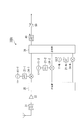
- FIG. 1 is a block diagram illustrating a receiver according to a first embodiment of the present invention. It is a block diagram which shows the detail of a structure of the receiver by the 1st Embodiment of this invention. It is a figure which shows operation
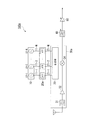
- FIG. 1 is a block diagram showing a configuration of a receiver according to the first embodiment of the present invention.
- a receiver 100 includes a local signal generation unit 10, a power phase adjustment unit 20, a frequency conversion unit 30, a frequency band limiting unit 40, a variable gain amplification unit 50, an analog / digital conversion unit 60, and a signal processing unit. 70 and a control unit 80.
- the local oscillation signal generator 10 generates and outputs local oscillation signals (local oscillation signals) having a plurality of set frequencies.
- the local signal generator 10 includes a plurality of local oscillators 11-1, 11-2,..., 11 that output a plurality of different frequencies LO-1, LO-2,. -N provided.
- the power phase adjustment unit 20 controls the power, frequency, and phase of the local oscillation signal supplied from the local oscillation signal generation unit 10 according to the setting, and outputs the result to the frequency conversion unit 30.
- the frequency conversion unit 30 performs frequency conversion on the radio signal received by the antenna.
- the frequency conversion unit 30 performs frequency conversion according to the local oscillation signal generated by the local oscillation signal generation unit 10 and supplied via the power phase adjustment unit 20, and performs a desired conversion in the baseband or intermediate frequency (IF) band. Arrange to frequency.
- the frequency conversion unit 30 can control the frequency arrangement in the baseband band or the IF band by this frequency conversion.
- the frequency conversion unit 30 can also adjust the gain of the frequency conversion according to the power, frequency, and phase of the input local oscillation signal.
- the frequency band limiting unit 40 limits the frequency band of the reception signal converted by the frequency conversion unit 30.
- the variable gain amplifier (VGA) 50 amplifies with a gain set according to the signal power of the received signal.
- the analog-to-digital converter 60 samples the supplied analog signal, converts it to a digital signal corresponding to the signal intensity, and generates a digital signal of time series data.
- the signal processing unit 70 processes various signals necessary for reception processing. That is, the signal processing unit 70 performs processing such as error control, decoding processing, and decompression processing on the received signal and monitoring of the received signal.
- the control unit 80 controls each unit of the receiver 100 in accordance with a setting signal from the host control unit or the like. Further, the control unit 80 may control each unit according to the signal power detected by the signal processing unit 70.
- FIG. 2 is a block diagram showing the configuration of the receiver in this embodiment.
- the receiver 100a includes a local oscillation signal generation unit 10, a power phase adjustment unit 20a, a frequency conversion unit 30a, a frequency band limiting unit 40, and a variable gain amplification unit (VGA) 50.
- the power phase adjustment unit 20a is a variable attenuation unit (ATT) 21-1, 21-2,... That attenuates the power of each local signal supplied from the local signal generation unit (LO) 10 according to the setting. 21-N (collectively “ATT21”).
- the ATT 21 is provided according to the local signal supplied from the local signal generator 10.
- the ATT 21 can set the attenuation rate independently of each other, and can perform the required power setting for each local signal.
- the frequency conversion unit 30 a includes a band pass filter 31, a low noise amplifier 32, a synthesis unit 33, and a mixer 34.
- the band pass filter (BPF) 31 is connected to the antenna, and extracts RF signals in the frequency band of the entire range to be received from the radio frequency (RF) signal received by the antenna.
- the low noise amplifier (LNA) 32 amplifies the RF signal filtered by the BPF 31.
- the synthesizer 33 synthesizes or combines the local signals supplied from the local signal generator 10 through the power phase adjuster 20a.
- the mixer 34 converts the RF signal into a baseband or IF band frequency by mixing the RF signal amplified by the LNA 32 with the local signal supplied from the LO 10.
- the frequency band limiting unit 40 is a filter having a low-pass characteristic or a transfer function having a band-pass characteristic. Even a filter having a transfer function having a low-pass characteristic exhibits a band-pass characteristic by a DC component removing capacitor or the like that cuts off a direct current (not shown), and therefore is shown as a filter having a transfer function having a band-pass characteristic in this figure.
- the cut-off frequency on the low frequency side in the transfer characteristic of the frequency band limiting unit 40 is determined by the band of the band-pass filter to be configured, or is determined by the cut-off frequency determined by the characteristic impedance of the circuit and the DC component removing capacitor.
- the cut-off frequency on the high frequency side in the transfer characteristic of the frequency band limiting unit 40 is determined according to the sampling frequency required for the digital signal performed in the subsequent stage.
- the frequency band limiting unit 40 extracts a signal in a required frequency band from the frequency-converted received signal.
- the local oscillation signal generation unit 10, the power phase adjustment unit 20a, the frequency band limiting unit 40, and the variable gain amplification unit (VGA) 50 function according to settings by the control unit 80 (FIG. 1).
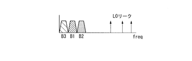
- FIG. 3A shows the channel arrangement of the RF signal and the frequency arrangement of the local oscillation signal supplied to the mixer 34 after being extracted by the BPF 31 and amplified by the LNA 32.
- the horizontal axis in FIG. 3A indicates the frequency range of the RF signal band, and the vertical axis indicates the signal power in each frequency band (band).
- This figure shows a state in which the RF signals of the bands B1 to B3 are received in order from the lowest frequency, and the RF signal of the band B3 shows a state where the signal power is larger than that of other channels.
- band B1 is arranged in the upper side band (USB) for the local oscillation signal of frequency LO-1
- band B2 is arranged in the lower side band (LSB) for the local oscillation signal of frequency LO-2
- band B3 is The LSB for the local signal of the frequency LO-3, which is arranged near the upper limit of the frequency band of the band B3.
- the frequency can be converted to a desired frequency in the baseband.
- the frequency arrangement so as not to interfere with each other, it is also possible to arrange the frequency bands in a low frequency region by narrowing the interval between the respective bands.
- the relationship between the frequency of the local oscillation signal and the frequency of each band before frequency conversion is set so that the bands after frequency conversion do not overlap each other.
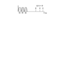
- FIG. 3B shows the result of frequency conversion of the signals in each band shown in FIG. 3A.
- the horizontal axis of FIG. 3B indicates the frequency range of the baseband signal band, and the vertical axis indicates the signal power at each frequency (channel).
- the signal shown in this figure is a signal that is frequency-converted by the frequency converting unit 30 and output via the frequency band limiting unit 40 and the VGA 50.
- the bands are arranged in the order of band B3, band B1, and band B2 from the vicinity of the direct current according to the frequency conversion result. Local signals leak and unwanted signals such as intermodulation distortion occur in the high frequency region, but their power is suppressed by the band limitation of the frequency band limiting unit 40.
- the power of the band B3 signal is attenuated to the same level as the signals of the other bands B1 and B2.
- the power of the frequency LO-3 is made relative to the frequencies LO-1 and LO-2 by increasing the attenuation amount of the ATT 21-3. There is a way to reduce it.
- the control unit 80 sets the power or frequency of the local oscillation signal of the LO 10 to suppress the signal of the channel with a large signal power, and each band has a limited frequency range. A signal can be placed.
- FIG. 4 is a block diagram showing a configuration of a receiver in the second embodiment of the present invention.
- the receiver 100b includes a plurality of local oscillators 11-1, 11-2,... 11-N corresponding to the local signal generator (LO) 10 in the first embodiment, and .., 21-N having a plurality of variable attenuation units (ATT) 21-1, 212-2,.
- LO local signal generator
- ATT variable attenuation units
- the receiver 100b further includes a plurality of mixers 34-1, 34-2,..., 34-N corresponding to the mixer 34 in the first embodiment.
- the frequency conversion unit 30b in the first embodiment includes a bandpass filter 31, a low noise amplifier 32, and mixers 34-1 to 34-N. Similar to the first embodiment, a frequency band limiting unit 40 and a variable gain amplifying unit 50 are connected to the frequency converting unit.
- the mixers 34-1 to 34-N correspond to the local oscillators 11-1 to 11-N of the local signal generator (LO) and the variable attenuators (ATT) 21-1 to 21-N of the power phase adjuster, respectively. Are provided separately.
- the mixers 34-1, 34-2,..., 34-N are connected to the output terminal of the LNA 32 and the input terminal of the frequency band limiting unit 40, respectively.
- the mixers 34-1, 34-2,..., 34-N perform frequency conversion on the signals supplied from the LNA 32 according to the supplied local signals, and frequency conversion to the baseband band.
- the signal is supplied to the frequency band limiting unit 40.
- FIG. 5 shows a circuit configuration of the mixers 34-1, 34-2,..., 34-N in the present embodiment.
- the same components as those in FIG. 4 are denoted by the same reference numerals.
- Each of the mixers 34-1, 34-2,..., 34-N shown in the figure includes a field effect transistor (FET) and a matching circuit. The source of each FET is grounded, the drain is commonly connected to the signal line, and the respective local signals LO-1, LO-2,..., LO-N are supplied to the gates.
- FET field effect transistor
- the conversion gain of the multiband RF signal supplied to the drain of the FET to the baseband can be changed. And a baseband signal can be output.
- Each of the mixers 11-1, 11-2,..., 21-N is controlled independently by the variable attenuators (ATT) 21-1, 21-2,.
- the conversion gain of 11-N can be controlled independently.
- FIG. 6 is a block diagram showing a configuration of a receiver according to the third embodiment of the present invention.
- the receiver 100c includes a plurality of local oscillators 11-1, 11-2,... 11-N corresponding to the local signal generator 10 in the first embodiment, and the first implementation. .., 21-N corresponding to the power phase adjusting unit 20a in the embodiment.
- the frequency conversion unit includes a band pass filter 31, a low noise amplifier 32, mixers 34-1 to 34-N, a demultiplexing unit 35, and a synthesis unit 36.
- a frequency band limiting unit 40 and a variable gain amplifying unit 50 are connected to the frequency converting unit.
- the demultiplexing unit 35 is provided between the LNA 32 and the mixers 34-1, 34-2,..., 34-N, and the multiband RF signal supplied from the LNA 32 for each corresponding frequency 3-4. Demultiplexed to 34-2,..., 34-N.
- the demultiplexing unit 35 may be configured by a distributor.
- the synthesizing unit 36 is provided between the mixers 34-1, 34-2,..., 34-N and the frequency band limiting unit 40, and the mixers 36-1, 34-2,.
- the supplied baseband signal is synthesized.
- the same operation as the configuration shown in FIG. 4 can be performed.
- the use of the demultiplexing unit 35 and the combining unit 36 can ensure the isolation between the mixers, increase the conversion gain, and reduce the generation power of unnecessary waves. There is.
- FIG. 7 is a block diagram showing the configuration of the receiver in this embodiment.
- the receiver 100d includes a local oscillation signal generation unit 10, a power phase adjustment unit 20a, a frequency conversion unit 30d, a frequency band limiting unit 40, and a variable gain amplification unit 50.
- the frequency converting unit 30d includes a bandpass filter 31, a low noise amplifier 32, mixers 34-1 and 34-2, a distributing unit 35, a combining unit 36d, and a distribution combining unit 37.
- the mixers 34-1 and 34-2 convert the RF signal into the frequency of the baseband signal by mixing the RF signal amplified by the LNA 32 with the local signal supplied from the LO 10.
- the mixers 34-1 and 34-2 are respectively supplied with local signals with a phase difference set to 90 degrees.
- the synthesizer 36d synthesizes the baseband signals supplied from the mixers 34-1 and 34-2.
- the combining unit 36d combines the signals input from one input terminal by rotating the phase by 90 degrees.
- the distribution / combination unit 37 performs two distributions and combination of a plurality of local oscillation signals supplied from the power phase adjustment unit 20b.
- the distribution / combination unit 37 sets a phase difference of 90 degrees with respect to each of the two local distribution signals.
- the frequency conversion unit 30d can perform frequency conversion with the configuration of the image suppression mixer. Since the frequency conversion unit 30d has a configuration of an image suppression mixer, it can reduce noise and unnecessary waves in the image band.
- the power phase adjustment units 21-1, 21-2,..., 21-N independently, the power of each LO signal in the mixers 34-1 and 34-2 can be controlled independently, and the corresponding LO The conversion gain of the mixer can be controlled independently for each frequency.
- FIG. 8A shows the channel arrangement of the RF signal and the frequency arrangement of the LO signal supplied to the mixer 34 after being extracted by the BPF 31 and amplified by the LNA 32.
- the horizontal axis in FIG. 8A indicates the frequency range of the RF signal band, and the vertical axis indicates the signal power in each frequency band (band).
- This figure shows a state in which the RF signals of the bands B1 to B3 are received in order from the lowest frequency, and the RF signal of the band B2 shows a state where the signal power is larger than that of other channels.
- the correspondence relationship between the frequencies LO-1, LO-2a (or LO-2b) and LO-3 of the local oscillation signal supplied from the LO 10 and the frequency band of the RF signal is also shown in this figure.
- the band B1 is arranged in the USB for the local oscillation signal of the frequency LO-1
- the band B2 is arranged in the USB for the local oscillation signal of the frequency LO-2a (or the LSB for the local oscillation signal of the frequency LO-2b).
- B3 is arranged in the USB for the local oscillation signal having the frequency LO-3.
- the frequency can be converted to a desired frequency in the baseband.
- the relationship between the frequency of the local oscillation signal and the frequency of each band before frequency conversion is set so that the bands after frequency conversion do not overlap each other.
- FIG. 8B shows the result of frequency conversion of the signals in each band shown in FIG. 8A.
- the horizontal axis of FIG. 8B indicates the frequency range of the baseband signal band, and the vertical axis indicates the signal power at each frequency (channel).
- the signal shown in this figure is a signal that is frequency-converted by the frequency converting unit 30 and output via the frequency band limiting unit 40 and the VGA 50.
- the bands are arranged in the order of band B3, band B1, and band B2 from the vicinity of the direct current according to the frequency conversion result.
- the power is attenuated to the same extent as the signals of the other bands B1 and B3.
- unnecessary signals such as local signal leakage and intermodulation distortion occur in the high frequency region, but the power of these unnecessary signals is suppressed by the frequency band limiting unit 40.
- a signal to be output to the output terminal is selected depending on whether the local signal is an LSB or a USB signal.
- Bands that are not selected have the same amplitude and opposite phase in the combining unit 36 and cancel each other.
- the attenuation characteristic due to the leak is positively utilized, and the signal power can be reduced by frequency-converting the signal in the band having a large signal power as a leak. It becomes possible to reduce the power difference from the signal power. As shown in FIG.
- the control unit 80 sets the frequency of the local oscillation signal of the LO 10 to suppress the signal power of the channel with a large signal power, and the signal of each band in a limited frequency range. Can be arranged.
- FIG. 9A shows the channel arrangement of the RF signal extracted by the BPF 31 and amplified by the LNA 32 and then supplied to the mixer 34.
- the horizontal axis of FIG. 9A indicates the frequency range of the RF signal band, and the vertical axis indicates the signal power in each frequency band (band).
- This figure shows a state in which the RF signals of the bands B1 to B3 are received in order from the lowest frequency, and the RF signal of the band B2 shows a state where the signal power is larger than that of other channels.
- the amplitude of the local oscillation signal having the frequency LO-2 is set smaller than that of other local oscillation signals by the power phase adjusting unit 20d.
- the band B1 is a USB for the local oscillation signal of the frequency LO-1, and is arranged near the lower limit of the frequency band of the band B1.
- Band B2 is arranged in the LSB for the local signal of frequency LO-2, and band B3 is arranged in the LSB for the local signal of frequency LO-3.
- each signal is converted into a frequency indicated by the difference between the frequency of each and the frequency of the local oscillation signal, and is arranged in the baseband.
- the frequencies LO-1 to LO-3 of the local oscillation signal are selected at appropriate intervals with respect to the frequencies of the bands B1 to B3, the frequency can be converted to a desired frequency in the baseband. It is also possible to arrange the band intervals side by side. At this time, the relationship between the frequency of the local oscillation signal and the frequency of each band before frequency conversion is set so that the bands after frequency conversion do not overlap each other.
- FIG. 9B shows the result of frequency conversion of the signals in each band shown in FIG. 9A.
- the horizontal axis of FIG. 9B indicates the frequency range of the baseband signal band, and the vertical axis indicates the signal power at each frequency (channel).
- the signal shown in this figure is a signal that is frequency-converted by the frequency converting unit 30 and output via the frequency band limiting unit 40 and the VGA 50.
- Each band is arranged in the order of band B1, band B3, and band B2 from the vicinity of the direct current according to the result of frequency conversion.
- the band B2 shows a state where power is attenuated as compared with the signals of the other bands B1 and B3.
- local signal leakage occurs in a high frequency region.
- the control unit 80 sets the frequency of the LO10 local oscillation signal and the attenuation factor of the power phase adjustment unit 20b, thereby suppressing the signal of the channel with a large signal power and being limited.
- the signals of the respective bands can be arranged in the specified frequency range.
- FIG. 10 is a block diagram showing the configuration of the receiver in this embodiment.
- the receiver 100e has a local signal generator (LO) composed of a plurality of local oscillators 11-1, 11-2,... 11-N. .., 11-N are preceded and followed by phase shifters 22-1, 22-2,..., 22-N (collectively referred to as phase shifter 22), And phase shifters 23-1, 23-2,..., 23-N (collectively referred to as phase shifter 23) are connected.
- LO local signal generator
- the phase shifters 22 and 23 constitute a power phase adjustment unit.
- the phase shifter 22 rotates the phase of the local oscillation signal supplied from the LO 10 by 90 degrees and outputs it.
- the phase shifter 23 transmits the phase of the local oscillation signal supplied from the LO 10 according to the setting or rotates it 180 degrees. That is, rotating the phase by 180 degrees is equivalent to inverting the supplied signal, and can be realized, for example, by providing one stage of a common-source amplifier having a gain of 0 dB (decibel).
- a frequency converter 30e is connected to the phase shifters 22 and 23.
- the frequency conversion unit 30e includes a bandpass filter 31, a low noise amplifier 32, synthesis units 33-1 and 33-2, mixers 34-1 and 34-2, a distribution unit 35, a synthesis unit 36d, and a variable gain amplifier (VGA) 38. Is provided.
- a band limiting unit 40 and a variable gain amplifying unit 50 are connected to the frequency converting unit 30e.
- the synthesizers 33-1 and 33-2 synthesize and output the local oscillation signals of different frequencies supplied.
- the variable gain amplifier (VGA) 38 amplifies the signal power required for frequency conversion.
- FIG. 11A shows the channel arrangement of the RF signal and the frequency arrangement of the local oscillation signal supplied to the mixer 34 after being extracted by the BPF 31 and amplified by the LNA 32.
- the horizontal axis in FIG. 11A indicates the frequency range of the RF signal band, and the vertical axis indicates the signal power in each frequency band (band).
- This figure shows a state in which the RF signals of the bands B1 to B3 are received in order from the lowest frequency, and the RF signal of the band B2 shows a state where the signal power is larger than that of other channels.
- each local oscillation signal is set to the same signal power.
- the band B1 is arranged in the LSB for the local oscillation signal of the frequency LO-1
- the band B2 is arranged in the USB for the local oscillation signal of the frequency LO-2
- the band B3 is the LSB for the local oscillation signal of the frequency LO-3. Placed in.
- each signal is converted to a frequency indicated by the difference between the frequency of each and the frequency of the local oscillation signal, and is arranged in the baseband.
- the frequency can be converted to a desired frequency in the baseband. It is also possible to arrange the band intervals side by side. At this time, the relationship between the frequency of the local oscillation signal and the frequency of each band before frequency conversion is set so that the bands after frequency conversion do not overlap each other.
- FIG. 11B shows the result of frequency conversion of the signals in each band shown in FIG. 11A.
- the horizontal axis in FIG. 11B indicates the frequency range of the baseband signal band, and the vertical axis indicates the signal power at each frequency (channel).
- the signal shown in this figure is a signal that is frequency-converted by the frequency converting unit 30 and output via the frequency band limiting unit 40 and the VGA 50.
- the bands are arranged in the order of band B3, band B1, and band B2 from the vicinity of the direct current according to the frequency conversion result.
- the band B2 shows a state where power is attenuated as compared with the signals of the other bands B1 and B3.
- unnecessary waves such as local signal leakage and intermodulation distortion occur in the high frequency region, but are suppressed by the frequency band limiting unit 40.
- phase shifter 23 when the phase setting of the phase shifter 23-2 corresponding to the local oscillation signal of the frequency LO-2 is switched from 0 degree to 180 degrees, the phase of the local oscillation signal input to the mixers 34-1 and 34-2 is changed. The angle is changed from (0, 90 degrees) to (180 degrees, 90 degrees).
- the distribution unit 35, the mixers 34-1 and 34-2, and the combining unit 36d constitute an image suppression mixer, the frequency band selected by the combining unit 36d can be switched from USB to LSB by the above-described phase switching. . That is, in the local oscillation signal of the frequency LO-2, the band B2 is USB, so in principle, they cancel each other out with the same amplitude and opposite phase and are canceled.
- band B2 having a large power is attenuated as a leak signal
- bands B1 and B3 are normally selected for local signals of other frequencies LO-1 and LO-3. It is possible to reduce the difference in signal power of all bands.
- the control unit 80 sets the frequency of the LO10 local oscillation signal and the phase of the phase shifter 23, thereby suppressing a signal of a channel with a large signal power and a limited frequency range.
- the signals of the respective bands can be arranged in.
- FIG. 12 is a block diagram showing the configuration of the receiver in this embodiment.
- the same components as those in the embodiment shown in FIGS. 1, 2, 7, and 10 are denoted by the same reference numerals.
- the receiver 100f shown in FIG. 12 includes a local oscillation signal generation unit (LO) 10f, a power phase adjustment unit 20f, a frequency conversion unit 30f, a frequency band limiting unit 40f, a variable gain amplification unit 50f, and an analog / digital conversion unit 60f.
- the local signal generator (LO) 10f includes a plurality of local oscillators 11-1 and 11-2 that output frequencies LO-1 and LO-2.
- the power phase adjustment unit 20f includes variable attenuation units (ATT) 21-1, 21-2, a selection unit 24, and a phase shifter 25.
- the selection unit (DPDT-SW) 24 is a double pole double throw type (DPDT type) selector switch. The selection unit 24 can select two input local oscillation signals and output them to one or both output terminals.
- the phase shifter 25 converts two input local oscillation signals into signals each having a phase difference of 90 degrees, and divides them into a local oscillation signal having a reference phase and a local oscillation signal having a phase of 90 degrees. To do.
- a local oscillation signal having a reference phase is supplied to the mixer 34-1 and a local oscillation signal having a phase of 90 degrees is supplied to the mixer 34-2.
- the frequency conversion unit 30f includes a bandpass filter 31, a low noise amplifier 32, mixers 34-1 and 34-2, a distribution unit 35, a variable gain amplifier (VGA) 38, and a distribution synthesizer 39.
- the distribution synthesizer 39 synthesizes two input signals with a phase difference of ⁇ 90 degrees, and divides them into two for output.
- the selection unit (DPDT-SW) 24 the LSB and USB output destination of each local signal can be switched to either signal A or signal B.
- the LSB having the frequency LO-1 can be changed to the signal A
- the USB can be changed to the signal B
- the USB having the frequency LO-2 can be changed to the terminal A
- the LSB can be changed to the signal B.
- the frequency band limiting unit 40f includes independent band pass filters (BPF) 41-1 and 41-2.
- the BPFs 41-1 and 41-2 have transfer characteristics in the same frequency band, but the passband gain, center frequency, and frequency bandwidth can be set according to the setting. In other words, when an excessive signal is input to the BPFs 41-1 and 41-2, the signal power output to the subsequent stage can be optimized by reducing the gain of the pass band.
- the variable gain amplifying unit 50f includes variable gain amplifiers 51-1 and 51-2, each of which can set an amplification factor independently. As described above, the signals A and B output from the frequency conversion unit 30f can be set independently by the frequency band limiting unit 40f and the variable gain amplification unit 50f. The signal power can be set.
- FIG. 13A shows the channel arrangement of the RF signal and the frequency arrangement of the local oscillation signal supplied to the mixer 34 after being extracted by the BPF 31 and amplified by the LNA 32.
- the horizontal axis indicates the frequency range of the RF signal band
- the vertical axis indicates the signal power in each frequency band (band).
- This figure shows a state in which the RF signals of the bands B1 to B3 are received in order from the lowest frequency, and the RF signal of the band B2 shows a state where the signal power is larger than that of other channels.
- each local oscillation signal is set to the same signal power.
- the band B1 is arranged in the LSB for the local oscillation signal having the frequency LO-1
- the band B2 is arranged in the USB for the local oscillation signal having the frequency LO-1.
- the local signal of frequency LO-1 selects a frequency between band B1 and band B2.
- Band B3 is arranged in the LSB for the local oscillation signal of frequency LO-2.
- the frequency of the local oscillation signal of the frequency LO-2 is selected so that the signal of the band B3 can be converted to a frequency lower than the frequency band that is half the frequency interval between the bands B1 and B2.
- each signal is converted into a frequency indicated by the difference between the frequency of each and the frequency of the local oscillation signal, and is arranged in the baseband.
- the frequencies LO-1 and LO-2 of the local oscillation signal are selected at appropriate intervals with respect to the frequencies of the bands B1 to B3, it can be converted into a desired frequency in the baseband. It is also possible to arrange the band intervals side by side. At this time, the relationship between the frequency of the local oscillation signal and the frequency of each band before frequency conversion is set so that the bands after frequency conversion do not overlap each other.
- 13B and 13C show the results of frequency conversion of the signals in each band shown in FIG. 13A, and show the signals A and B output from the frequency conversion unit 30f, respectively.
- the horizontal axis indicates the frequency range of the baseband signal band, and the vertical axis indicates the signal power at each frequency (channel).
- the signal shown in this figure is a signal that is frequency-converted by the frequency converting unit 30f and output through the frequency band limiting unit 40f and the VGA 50f.
- the band of the band B2 is arranged in the signal B in the order of the band B3 and the band B1 from the vicinity of the direct current in the signal A.
- the signal power is attenuated as compared with the signals of the other bands B1 and B3 by increasing the attenuation amounts of the frequency band limiting unit 41-2 and the variable gain amplifying unit 51-2. It is possible to reduce the power difference from the signal power of other bands.
- the above is an example in which only the band B2 is attenuated, but the attenuation of the variable attenuation units (ATT) 21-1, 21-2, the setting of the selection unit (DPDT-SW) 24, the frequency band limiting unit 41f, and the variable gain amplification
- the conversion gains of the three bands B1, B2, and B3 can be controlled independently.
- the frequency of the LO10f local oscillation signal, the attenuation rate and frequency switching of the power phase adjustment unit 20f, and the setting of the attenuation rates of the frequency band limiting unit 40f and the variable gain amplification unit 50f are controlled by the control unit.
- the control unit By setting 80 respectively, it is possible to suppress a signal of a channel having a large signal power and to arrange a signal of each band in a limited frequency range.
- FIG. 14 is a block diagram showing a configuration of a receiver according to the eighth embodiment of the present invention.
- the receiver 100g includes a local signal generator (LO) 10g, a power phase adjuster 20a, a frequency converter 30d, a frequency band limiter 40, and a variable gain amplifier 50.
- LO 10g is a local signal generator 11-1,..., 11-M (collectively referred to as a local signal generator 11), a direct digital synthesizer (DDS) 12-1, 12-2,. N (collectively referred to as DDS12).
- the local signal generator 11 supplies the original clock signal of the DDS 12.
- the DDS 12 uses the frequency of the supplied source clock signal as a reference signal and outputs a local oscillation signal having a desired frequency according to the setting. Thereby, it can be used as a frequency variable local oscillation signal generator with a high switching speed.
- the configuration described above can be applied in place of the LO 10 of each of the embodiments described above. As a result, the number of original clocks can be reduced, and the degree of freedom of the frequency setting range of the generated local signals can be increased. Therefore, the receiver can be configured without providing a plurality of local signal generators fixedly. be able to.
- FIG. 15 is a block diagram showing a configuration of a receiver according to the ninth embodiment of the present invention.
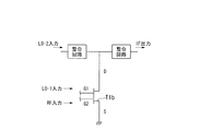
- the receiver 100 h includes a local oscillation signal generation unit (LO) 10 f, a power phase adjustment unit 20 h, a frequency conversion unit 30 h, a frequency band limiting unit 40, and a variable gain amplification unit 50.
- the power phase adjustment unit 20h includes variable attenuation units (ATT) 21-1 and 21-2.
- the frequency conversion unit 30h includes a band pass filter 31, a low noise amplifier 32, and a mixer 34DP.
- the mixer 34DP has an input terminal to which two local oscillation signals are input, and performs frequency conversion according to the local oscillation signals of two frequencies that are input without providing a synthesizer outside.
- a dual gate transistor T1a is used for the mixer 34DP.
- the source is grounded, the drain is connected to the signal line, and the local oscillation signals LO-1 and LO-2 are supplied to the two gates.
- the amplification factor of the multiband RF signal supplied to the drain can be changed according to the two local oscillation signals supplied to the gate of the dual gate transistor T1a.
- frequency conversion as a mixer can be performed according to the local signals LO-1 and LO-2, and baseband signals can be output.
- a dual gate transistor T1b is used for the mixer 34DP.
- the dual gate transistor T1b has a source grounded and a drain supplied with one local oscillation signal LO-1 and connected to a signal output terminal. Further, the other local oscillation signal LO-2 and the multiband RF signal are supplied to the two gates. The amplification factor of the multiband RF signal supplied to the other gate can be changed according to the two local oscillation signals supplied to the drain and one gate of the dual gate transistor T1b. Further, frequency conversion as a mixer can be performed according to the local signals LO-1 and LO-2, and baseband signals can be output.
- the RF signal is described as being converted into a baseband signal.
- the RF signal may be converted into an IF signal instead of the baseband signal.
- a signal in a band with a large signal power is arranged in the cutoff frequency region on the low cutoff frequency side such as BPF41. Can be done.
- a configuration in which the DC component is removed may be employed.
- the local signal generation unit 10 of the receiver that performs frequency conversion of signals included in a plurality of radio frequency bands supplies a plurality of local signals.
- the power phase adjustment unit 20 adjusts the absolute power or the relative phase of the local signal.
- the frequency conversion unit 30 converts the frequency of the radio frequency band using a local signal and rearranges the frequency within a desired frequency region. Thereby, the receiver 100 can suppress an increase in circuit scale even when the corresponding radio frequency band is increased.
- the frequency conversion unit 30 may select at least one of the lower sideband (LSB) region and the upper sideband (USB) region of the local oscillation signal according to the relative phase difference of the local oscillation signal.
- the frequency of the signal included in the frequency domain is converted.
- the frequency conversion unit 30 can extract a signal included in at least one frequency region of the lower sideband (LSB) region or the upper sideband (USB) region of the local oscillation signal.
- the frequency converter 30 separates signals included in the lower sideband (LSB) region or the upper sideband (USB) region of the local oscillation signal and sets the amplification factor, so that a plurality of reception bands are collected. Can be processed.
- the frequency conversion unit 30 performs frequency conversion based on the local oscillation signal, performs image suppression, or separates the lower sideband (LSB) and the upper sideband (USB). Output.
- the frequency conversion unit 30 can extract a signal included in the frequency region of the lower sideband (LSB) region or the upper sideband (USB) region of the local oscillation signal by performing image suppression.
- the frequency converter 30 separates signals included in the lower sideband (LSB) region or the upper sideband (USB) region of the local oscillation signal and sets the amplification factor, so that a plurality of reception bands are collected. Can be processed.
- the power phase adjustment unit 20 generates and supplies a pair of local oscillation signals having orthogonal phase differences based on the local oscillation signals. As a result, the power phase adjustment unit 20 can generate a pair of local oscillation signals having orthogonal phase differences based on the local oscillation signals.
- the electric power phase adjustment part 20 is provided with the phase shifter 23 which switches the relative phase difference of the local oscillation signal which has an orthogonal phase difference.
- the power phase adjustment unit 20 switches the relative phase difference between the local signals having orthogonal phase differences, thereby extracting the signal to be extracted from the lower sideband (LSB) region or the upper sideband (USB) of the local signal. ) It can be switched and extracted as a region signal.
- the frequency conversion unit 30 has at least one frequency region of the lower sideband (LSB) region or the upper sideband (USB) region of the local oscillation signal according to the frequency of the local oscillation signal.
- the frequency of the signal contained in is converted.
- the frequency converter 30 can extract a signal included in at least one frequency region of the lower sideband (LSB) region or the upper sideband (USB) region of the local oscillation signal.
- the frequency conversion unit 30 separates signals included in the lower sideband (LSB) region or the upper sideband (USB) region of the local oscillation signal and sets the amplification factor, so that a plurality of reception bands are collected. Can be processed.
- the signal processing unit 70 detects power for each frequency band in which a radio signal whose frequency is converted is included.
- the control unit 80 reduces the power difference for each frequency band of the radio signal according to the detected power, and the local signal corresponding to the frequency band is arranged so that the interval on the frequency axis of the radio signal is narrowed.
- the attenuation amount for attenuating the power of at least one of the frequency and the relative phase difference of the local signal is adjusted.
- the power for each frequency band is detected by the signal processing unit 70, and the control unit 80 suppresses an excessive signal or adjusts the balance of the signal power based on the magnitude of the signal power for each frequency band. It becomes possible to do.
- frequency conversion can be performed to increase the efficiency of frequency arrangement, and signals arranged in a plurality of frequency bands can be converted into signals with a limited amount of information.
- the signal processing unit 70 is arranged at a location different from the frequency conversion unit 30, and the signal frequency-converted by the frequency conversion unit 30 is transmitted by the transmission unit and supplied.
- the receiver 100 can separate the place where the radio signal is received from the place where the signal processing unit 70 is arranged, and transmits the received signal and control signal by providing the necessary transmission means.
- the transmission means only needs to be able to transmit the frequency band of the signal converted from the conversion of the radio signal to the frequency into the baseband signal, and can be easily configured as compared with the configuration of receiving the broadband radio signal as it is. .
- the transmission means may select either an analog signal transmission method or a digital signal transmission method.
- the configuration shown in the above embodiment can be changed in quantity, combination, and the like within a range that does not change the characteristics of the present invention.
- the signal processing unit 70 and the control unit 80 can be configured to include a processing device such as a CPU that operates based on a stored program, and control each unit of the receiver 100 based on the program. Can do. Further, the signal processing unit 70 and the control unit 80 may be processed by the same CPU.
- the present invention can be applied to a receiver that performs communication using a plurality of radio bands, and can suppress an increase in circuit scale even when the corresponding radio frequency band is increased.
Landscapes
- Engineering & Computer Science (AREA)
- Computer Networks & Wireless Communication (AREA)
- Signal Processing (AREA)
- Superheterodyne Receivers (AREA)
Abstract
受信機は、局発信号生成部と電力位相調整部と周波数変換部とを有し、複数の無線周波数帯に含まれる信号の周波数変換を行う。局発信号生成部は、複数の局発信号を供給する。電力位相調整部は、局発信号の電力又は局発信号の相対的な位相を調整する。周波数変換部は、電力位相調整部によって調整された局発信号を用いて無線周波数帯の周波数を変換して所望の周波数領域内に並び替える。
Description
本発明は、複数の無線帯域を用いて通信を行う受信機に関する。
本願は、2010年1月12日に、日本に出願された特願2010-4325号に基づき優先権を主張し、その内容をここに援用する。
本願は、2010年1月12日に、日本に出願された特願2010-4325号に基づき優先権を主張し、その内容をここに援用する。
無線通信の用途が多様化するのにしたがって、複数の周波数帯域の信号を受信できる受信機(マルチバンド受信機)では、受信帯域の広帯域化が必要とされる。
従来のマルチバンド受信機は、複数の無線周波数帯域ごとに周波数帯域を分割して、それぞれの周波数帯域ごとに受信ミキサを設ける場合や、同時に受信できる無線周波数帯域の数を限定し、必要とされる数の受信回路を設ける場合がある(例えば、非特許文献1から2参照)。
従来のマルチバンド受信機は、複数の無線周波数帯域ごとに周波数帯域を分割して、それぞれの周波数帯域ごとに受信ミキサを設ける場合や、同時に受信できる無線周波数帯域の数を限定し、必要とされる数の受信回路を設ける場合がある(例えば、非特許文献1から2参照)。
伊藤他、「携帯電話とそのシステムの徹底研究」、CQ出版社、RFワールド No.2、p57、2008年4月.
栗原淳、鈴木博、「RFフィルタ・バンクを用いたソフトウェア無線受信機」電子情報通信学会 信学技報RCS2004-133、2004年8月.
しかしながら、非特許文献1の技術において、対応する無線周波数帯域に応じて受信回路を設ける形態では、対応する無線周波数帯域が増えると、回路規模が増大してしまうという問題が生じる。
本発明はこのような事情に鑑みてなされたもので、対応する無線周波数帯域を増やした場合においても回路規模の増大を抑圧できる受信機を提供することにある。
本発明は、上述した課題を解決するためになされたものである。本発明は、複数の無線周波数帯に含まれる信号の周波数変換を行う受信機であって、複数の局発信号を供給する局発信号生成部と、前記局発信号の電力又は相対的な位相を調整する調整部と、前記調整された局発信号を用いて前記複数の無線周波数帯の周波数を同時に変換して所望の周波数領域内に並び替える周波数変換部とを備える。
本発明の受信機において、前記周波数変換部は、前記局発信号の相対位相差に応じて、前記局発信号の下側波帯(LSB)領域又は上側波帯(USB)領域の少なくともいずれかの周波数領域に含まれる前記信号の周波数を変換することが好ましい。
また、本発明の受信機において、前記周波数変換部は、前記局発信号に基づいて周波数変換を行うとともに、イメージ抑圧を行う、又は、下側波帯(LSB)と上側波帯(USB)を分離して出力することが好ましい。
また、本発明の受信機において、前記調整部は、前記局発信号に基づいて直交する位相差を有して対となる局発信号を生成してそれぞれ供給することが好ましい。
また、本発明の受信機において、前記調整部は、前記直交する位相差を有する局発信号の相対位相差を切り替える相対位相差設定部を備えることが好ましい。
また、本発明の受信機において、前記周波数変換部は、前記局発信号の周波数に応じて、前記局発信号の下側波帯(LSB)領域又は上側波帯(USB)領域の少なくともいずれかの周波数領域に含まれる前記信号の周波数を変換することが好ましい。
また、本発明の受信機において、前記局発信号生成部は、前記局発信号を供給するダイレクトデジタルシンセサイザ部を備えることが好ましい。
また、本発明の受信機において、前記周波数が変換された信号が含まれる周波数帯域ごとの電力を検出する信号処理部と、前記検出された電力に応じて、前記信号の周波数帯域ごとの電力差を低減し前記信号の周波数軸上の間隔を狭めて配置するように、周波数帯域に対応する前記局発信号の電力を減衰させる減衰量、或いは、該局発信号の周波数又は相対位相差の少なくともいずれか1つを調整する制御部とを備えることが好ましい。
また、本発明の受信機において、前記信号処理部は、前記周波数変換部と異なる場所に配置され、前記周波数変換部によって周波数変換された信号が伝送手段によって伝送され供給されることが好ましい。
さらにまた、本発明は、複数の無線周波数帯の信号を受信する受信機であって、複数の局発信号源にそれぞれ接続され信号電力又は位相を調整する調整部と、前記調整部により各々信号電力又は位相が調整された複数の局発信号を合成する合成部と、前記複数の無線周波数帯の信号を受信するアンテナに接続され所望の前記複数の無線周波数帯の信号を通過させるバンドパスフィルタと、前記バンドパスフィルタに接続される低雑音増幅器と、前記低雑音増幅器の出力端子に接続され前記合成部により合成された前記複数の局発信号に周波数変換を行うミキサと、前記ミキサにより周波数変換された信号が供給されるフィルタと、前記フィルタに接続される可変利得増幅部とを備える。
この発明によれば、受信機は、複数の無線周波数帯に含まれる信号の周波数変換を同時に行う。局発信号生成部は、複数の局発信号を供給する。調整部は、局発信号の電力又は相対的な位相を調整する。周波数変換部は、局発信号を用いて前記無線周波数帯の周波数を同時に変換して所望の周波数領域内に並び替える。
これにより、受信機は、対応する無線周波数帯域を増やした場合においても回路規模の増大を抑圧することが可能となる。
これにより、受信機は、対応する無線周波数帯域を増やした場合においても回路規模の増大を抑圧することが可能となる。
以下、本発明の一実施形態を、図面を参照して説明する。
(第1実施形態)
図1は、本発明の第1の実施形態による受信機の構成を示すブロック図である。
図1を参照すると、受信機100は、局発信号生成部10、電力位相調整部20、周波数変換部30、周波数帯域制限部40、可変利得増幅部50、アナログデジタル変換部60、信号処理部70、および制御部80を備える。
局発信号生成部10は、設定された複数の周波数の局部発振信号(局発信号)を生成し、出力する。局発信号生成部10は、各々異なる複数の周波数LO-1、LO-2、・・・、およびLO-Nを出力する複数の局部発振器11-1、11-2、・・・、および11-Nを備える。
電力位相調整部20は、局発信号生成部10から供給される局発信号の電力、周波数、および位相を設定に応じて制御して、周波数変換部30に出力する。
周波数変換部30は、アンテナによって受信した無線信号に対して周波数変換を行う。周波数変換部30は、局発信号生成部10によって生成され、電力位相調整部20を介して供給される局発信号に応じた周波数変換を行い、ベースバンド又は中間周波数(IF)帯域における所望の周波数に配置する。周波数変換部30は、この周波数変換により、ベースバンド帯域又はIF帯における周波数配置を制御することができる。また、周波数変換部30は、周波数変換のほかに、入力される局発信号の電力、周波数、および位相に応じて周波数変換の利得を調整することもできる。
周波数帯域制限部40は、周波数変換部30によって変換された受信信号の周波数帯域を制限する。
可変利得増幅部(VGA)50は、受信信号の信号電力に応じて設定される増幅率で増幅する。
アナログデジタル変換部60は、供給されるアナログ信号のサンプリングを行い、信号強度に応じたデジタル信号に変換し、時系列データのデジタル信号を生成する。
信号処理部70は、受信処理に必要とされる各種信号の処理を行う。すなわち、信号処理部70は、受信信号に対する誤り制御、復号化処理、伸張処理などの処理や受信信号の監視などの処理を行う。
制御部80は、上位制御部などからの設定信号に応じて、受信機100の各部の制御を行う。また、制御部80は、信号処理部70によって検出された信号電力に応じて、各部の制御を行っても良い。
本実施形態における受信機のより具体的な構成例を示す。
図2は、本実施形態における受信機の構成を示すブロック図である。図1と同じ構成には、同じ符号を付す。
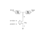
図2を参照すると、受信機100aは、局発信号生成部10、電力位相調整部20a、周波数変換部30a、周波数帯域制限部40及び可変利得増幅部(VGA)50を備える。
電力位相調整部20aは、局発信号生成部(LO)10から供給される各局発信号の電力を設定に応じて減衰させる可変減衰部(ATT)21-1、21-2、・・・、21-N(まとめて「ATT21」という)を備える。ATT21は、局発信号生成部10から供給される局発信号に応じて設けられる。ATT21は、それぞれ独立に減衰率を設定でき、それぞれの局発信号に対して必要とされる電力設定を行うことができる。
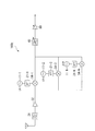
周波数変換部30aは、バンドパスフィルタ31、ローノイズアンプ32、合成部33、およびミキサ34を備える。
バンドパスフィルタ(BPF)31は、アンテナに接続され、アンテナによって受信された高周波(RF)信号から、受信対象とする全ての範囲の周波数帯域のRF信号を抽出する。
ローノイズアンプ(LNA)32は、BPF31によってフィルタリングされたRF信号を増幅する。
合成部33は、局発信号生成部10から電力位相調整部20aを介して供給される局発信号を合成又は合波する。
ミキサ34は、LNA32によって増幅されたRF信号を、LO10から供給される局発信号と混合することによって、RF信号をベースバンド又はIF帯の周波数に変換する。
図2は、本実施形態における受信機の構成を示すブロック図である。図1と同じ構成には、同じ符号を付す。
図2を参照すると、受信機100aは、局発信号生成部10、電力位相調整部20a、周波数変換部30a、周波数帯域制限部40及び可変利得増幅部(VGA)50を備える。
電力位相調整部20aは、局発信号生成部(LO)10から供給される各局発信号の電力を設定に応じて減衰させる可変減衰部(ATT)21-1、21-2、・・・、21-N(まとめて「ATT21」という)を備える。ATT21は、局発信号生成部10から供給される局発信号に応じて設けられる。ATT21は、それぞれ独立に減衰率を設定でき、それぞれの局発信号に対して必要とされる電力設定を行うことができる。
周波数変換部30aは、バンドパスフィルタ31、ローノイズアンプ32、合成部33、およびミキサ34を備える。
バンドパスフィルタ(BPF)31は、アンテナに接続され、アンテナによって受信された高周波(RF)信号から、受信対象とする全ての範囲の周波数帯域のRF信号を抽出する。
ローノイズアンプ(LNA)32は、BPF31によってフィルタリングされたRF信号を増幅する。
合成部33は、局発信号生成部10から電力位相調整部20aを介して供給される局発信号を合成又は合波する。
ミキサ34は、LNA32によって増幅されたRF信号を、LO10から供給される局発信号と混合することによって、RF信号をベースバンド又はIF帯の周波数に変換する。
周波数帯域制限部40は、ローパス特性又はバンドパス特性の伝達関数を有するフィルタである。ローパス特性の伝達関数を有するフィルタであっても、図示されない直流を遮断する直流成分除去コンデンサなどによってバンドパス特性を呈するため、この図ではバンドパス特性の伝達関数を有するフィルタとして示す。周波数帯域制限部40の伝達特性における低域側のカットオフ周波数は、構成するバンドパスフィルタの帯域で定められるか、回路の特性インピーダンスと直流成分除去コンデンサなどによって定められるカットオフ周波数によって定められる。また、周波数帯域制限部40の伝達特性における高域側のカットオフ周波数は、後段で行われるデジタル信号化に必要とされるサンプリング周波数に応じて定められる。周波数帯域制限部40は、周波数変換された受信信号から必要とされる周波数帯域の信号を抽出する。
局発信号生成部10、電力位相調整部20a、周波数帯域制限部40及び可変利得増幅部(VGA)50は、制御部80(図1)による設定によって機能する。
局発信号生成部10、電力位相調整部20a、周波数帯域制限部40及び可変利得増幅部(VGA)50は、制御部80(図1)による設定によって機能する。
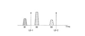
次に図3Aおよび図3Bを参照して、本実施形態の受信機における周波数変換について説明する。
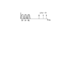
図3Aは、BPF31によって抽出され、LNA32によって増幅された後に、ミキサ34に供給されるRF信号のチャネル配置及び局発信号の周波数配置を示す。図3Aの横軸は、RF信号帯域の周波数範囲を示し、縦軸は各周波数帯(バンド)における信号電力を示す。
この図においては、周波数の低い方から順に、バンドB1からB3のRF信号を受信している状態を示し、バンドB3のRF信号が、他のチャネルより信号電力が大きい状態を示す。
図3Aは、BPF31によって抽出され、LNA32によって増幅された後に、ミキサ34に供給されるRF信号のチャネル配置及び局発信号の周波数配置を示す。図3Aの横軸は、RF信号帯域の周波数範囲を示し、縦軸は各周波数帯(バンド)における信号電力を示す。
この図においては、周波数の低い方から順に、バンドB1からB3のRF信号を受信している状態を示し、バンドB3のRF信号が、他のチャネルより信号電力が大きい状態を示す。
また、LO10から供給される局発信号の各周波数LO-1、LO-2、LO-3と、RF信号の周波数帯との対応関係をこの図に併せて示す。
バンドB1は、周波数LO-1の局発信号に対する上側波帯(USB)に配置され、バンドB2は、周波数LO-2の局発信号に対する下側波帯(LSB)に配置され、バンドB3は、周波数LO-3の局発信号に対するLSBであって、バンドB3の周波数帯域の上限付近に配置される。周波数変換部30によって周波数変換される場合に、各信号は、それぞれの周波数と局発信号の周波数との差によって示される周波数に変換され、ベースバンド帯域に配置される。バンドB1からB3の周波数に対して局発信号の周波数LO-1からLO-3を適当な間隔で選択することにより、ベースバンド帯域の所望の周波数に変換できる。これにより、相互に干渉しないように周波数配置を定めることにより、周波数の低い領域にそれぞれの帯域の間隔を狭めて並べて配置することも可能である。その際、周波数変換後の帯域が互いに重ならないように、局発信号の周波数と周波数変換前の各帯域の周波数の関係を設定する。
バンドB1は、周波数LO-1の局発信号に対する上側波帯(USB)に配置され、バンドB2は、周波数LO-2の局発信号に対する下側波帯(LSB)に配置され、バンドB3は、周波数LO-3の局発信号に対するLSBであって、バンドB3の周波数帯域の上限付近に配置される。周波数変換部30によって周波数変換される場合に、各信号は、それぞれの周波数と局発信号の周波数との差によって示される周波数に変換され、ベースバンド帯域に配置される。バンドB1からB3の周波数に対して局発信号の周波数LO-1からLO-3を適当な間隔で選択することにより、ベースバンド帯域の所望の周波数に変換できる。これにより、相互に干渉しないように周波数配置を定めることにより、周波数の低い領域にそれぞれの帯域の間隔を狭めて並べて配置することも可能である。その際、周波数変換後の帯域が互いに重ならないように、局発信号の周波数と周波数変換前の各帯域の周波数の関係を設定する。
図3Bは、図3Aに示された各帯域の信号を周波数変換した結果を示す。
この図3Bの横軸は、ベースバンド信号帯域の周波数範囲を示し、縦軸は各周波数(チャネル)における信号電力を示す。この図に示された信号は、周波数変換部30によって周波数変換され、周波数帯域制限部40及びVGA50を介して出力される信号である。
周波数変換の結果により直流付近から、バンドB3、バンドB1、バンドB2の順にそれぞれの帯域が配置される。周波数の高い領域に局発信号のリークや、混変調ひずみ等の不要信号が生じるが、周波数帯域制限部40の帯域制限によりそれらの電力は抑圧される。
バンドB3の信号については、他のバンドB1およびB2の信号と同レベルにまで電力が減衰している。このように、バンドB3の変換利得をバンドB1およびB2より下げる方法としては、ATT21-3の減衰量を大きくすることで、周波数LO-3の電力を周波数LO-1およびLO-2に対し相対的に低下させる方法がある。
また、周波数帯域制限部40及び直流成分除去コンデンサによって定められる低域側のカットオフ周波数より、最も低周波数側に配置されたバンドB3の帯域の少なくとも一部を低周波数側に配置することでも、バンドB3の信号の電力を減衰させることができ、他のバンドの電力と整合させることが可能となる。
以上に示したように、LO10の局発信号の電力又は周波数を、制御部80がそれぞれ設定することにより、信号電力が大きいチャネルの信号を抑圧するとともに、限られた周波数範囲にそれぞれの帯域の信号を配置することができる。
以上に示したように、LO10の局発信号の電力又は周波数を、制御部80がそれぞれ設定することにより、信号電力が大きいチャネルの信号を抑圧するとともに、限られた周波数範囲にそれぞれの帯域の信号を配置することができる。
(第2実施形態)
次に、図4を参照して、本発明の第2の実施形態による受信機について説明する。
図4は、本発明の第2の実施形態における受信機の構成を示すブロック図である。図1および図2に示された第1の実施形態と同じ構成要素には、同じ符号を付す。
図4を参照すると、受信機100bは、第1の実施形態における局発信号生成部(LO)10に相当する複数の局部発振器11-1、11-2、・・・11-N、および第1の実施形態における電力位相調整部20aに相当する複数の可変減衰部(ATT)21-1,21-2・・・21-Nを有する。受信機100bは、さらに、第1の実施形態におけるミキサ34に相当する複数のミキサ34-1、34-2、・・・、34-Nを有する。 第1の実施形態における周波数変換部30bは、本実施例においてはバンドパスフィルタ31、ローノイズアンプ32、およびミキサ34-1~34-Nによって構成される。第1の実施形態と同様に、この周波数変換部には、周波数帯域制限部40及び可変利得増幅部50が接続される。
ミキサ34-1~34-Nは、局発信号生成部(LO)の局部発振器11-1~11-N及び電力位相調整部の可変減衰部(ATT)21-1~21-Nに各々対応して個別に設けられる。
ミキサ34-1、34-2、・・・、34-Nは、それぞれLNA32の出力端子と周波数帯域制限部40の入力端子にそれぞれ接続される。ミキサ34-1、34-2、・・・、34-Nは、LNA32からそれぞれ供給される信号に対して、それぞれ供給される局発信号に応じて周波数変換を行い、ベースバンド帯域に周波数変換された信号を周波数帯域制限部40に供給する。
図5を参照して、本実施形態におけるミキサのより具体的な構成について説明する。
図5は、本実施形態におけるミキサ34-1、34-2、・・・、34-Nの回路構成を示す。図4と同じ構成には、同じ符号を付す。 この図に示されるミキサ34-1、34-2、・・・、34-Nのそれぞれは、電界効果型トランジスタ(FET)と整合回路とを含んで構成される。各FETのソースが接地され、ドレインが信号線に共通に接続され、ゲートには、それぞれの局発信号LO-1、LO-2、・・・、LO-Nが供給される。FETのゲートに供給される局発信号に応じて、FETのドレインに供給されるマルチバンドRF信号のベースバンド帯への変換利得をそれぞれ変化させることができ、ミキサとしての周波数変換を各局発信号に応じて行い、ベースバンド信号を出力することができる。
電力位相調整部20の可変減衰部(ATT)21-1、21-2、・・・、21-Nを各々独立に制御することで、各ミキサ11-1、11-2、・・・、11-Nの変換利得を独立に制御できる。
(第3実施形態)
図6を参照して、本発明の第3の実施形態による受信機について説明する。
図6は、本発明の第3の実施形態による受信機の構成を示すブロック図である。図1、図2および図4に示された実施形態と同じ構成要素には、同じ符号を付す。
図6を参照すると、受信機100cは、第1の実施形態における局発信号生成部10に相当する複数の局部発振器11-1、11-2、・・・11-N、および第1の実施形態における電力位相調整部20aに相当する複数の可変減衰部(ATT)21-1,21-2・・・21-Nを有する。
周波数変換部は、バンドパスフィルタ31、ローノイズアンプ32、ミキサ34-1~34-N、分波部35、および合成部36から構成される。この周波数変換部には、周波数帯域制限部40及び可変利得増幅部50が接続される。
分波部35は、LNA32とミキサ34-1、34-2、・・・、34-N間に設けられ、LNA32から供給されるマルチバンドRF信号を対応する周波数ごとに各ミキサ34-1、34-2、・・・、34-Nに分波する。なお、分波部35は、分配器によって構成しても良い。
合成部36は、ミキサ34-1、34-2、・・・、34-Nと周波数帯域制限部40間に設けられ、各ミキサ34-1、34-2、・・・、34-Nから供給されるベースバンド信号を合成する。
この図に示した構成では、図4に示した構成と同様の動作を行わせることができる。図4の構成に比べて、分波部35と合成部36を用いることにより、各ミキサ間のアイソレーションを確保することができ、変換利得を増加させたり、不要波の発生電力を低減できる利点がある。
(第4実施形態)
図7を参照して、本発明の第4の実施形態による受信機について説明する。
図7は、本実施形態における受信機の構成を示すブロック図である。図1、図2、および図6に示された実施形態と同じ構成要素には、同じ符号を付す。
図7を参照すると、受信機100dは、局発信号生成部10、電力位相調整部20a、周波数変換部30d、周波数帯域制限部40、および可変利得増幅部50を備える。
周波数変換部30dは、バンドパスフィルタ31、ローノイズアンプ32、ミキサ34-1、34-2、分配部35、合成部36d、および分配合成部37を備える。
ミキサ34-1、34-2は、LNA32によって増幅されたRF信号を、LO10から供給される局発信号と混合することによって、RF信号をベースバンド信号の周波数に変換する。ミキサ34-1、34-2には、位相差が90度に設定された局発信号がそれぞれ供給される。
合成部36dは、ミキサ34-1、34-2から供給されるベースバンド信号を合成する。合成部36dは、一方の入力端子から入力される信号の位相を90度回転し合成する。
分配合成部37は、電力位相調整部20bから供給される複数の局発信号の2分配と合成を行う。分配合成部37は、2分配された一方の各局発信号に対して90度の位相差を設定する。
以上の構成により周波数変換部30dは、イメージ抑圧ミキサの構成により周波数変換を行うことができる。周波数変換部30dは、イメージ抑圧ミキサの構成としたことにより、イメージ帯域のノイズと不要波を低減することができる。
電力位相調整部21-1、21-2、・・・、21-Nを独立に制御することで、ミキサ34-1、34-2における各LO信号の電力を独立に制御でき、対応するLO周波数ごとにミキサの変換利得を各々独立に制御できる。
図8Aおよび8Bを参照して、本実施形態に示す受信機における周波数変換について説明する。
図8Aは、BPF31によって抽出され、LNA32によって増幅された後に、ミキサ34に供給されるRF信号のチャネル配置及びLO信号の周波数配置を示す。図8Aの横軸は、RF信号帯域の周波数範囲を示し、縦軸は各周波数帯(バンド)における信号電力を示す。
この図においては、周波数の低いほうから順に、バンドB1からB3のRF信号を受信している状態を示し、バンドB2のRF信号が、他のチャネルより信号電力が大きい状態を示す。
図8Aは、BPF31によって抽出され、LNA32によって増幅された後に、ミキサ34に供給されるRF信号のチャネル配置及びLO信号の周波数配置を示す。図8Aの横軸は、RF信号帯域の周波数範囲を示し、縦軸は各周波数帯(バンド)における信号電力を示す。
この図においては、周波数の低いほうから順に、バンドB1からB3のRF信号を受信している状態を示し、バンドB2のRF信号が、他のチャネルより信号電力が大きい状態を示す。
また、LO10から供給される局発信号の各周波数LO-1、LO-2a(又はLO-2b)、LO-3と、RF信号の周波数帯との対応関係をこの図に併せて示す。
バンドB1は、周波数LO-1の局発信号に対するUSBに配置され、バンドB2は、周波数LO-2aの局発信号に対するUSB(或いは周波数LO-2bの局発信号に対するLSB)に配置され、バンドB3は、周波数LO-3の局発信号に対するUSBに配置される。
周波数変換部30dによって周波数変換される場合に、各信号は、それぞれの周波数と局発信号の周波数との差によって示される周波数に変換され、ベースバンド帯域に配置される。バンドB1からB3の周波数に対して局発信号の周波数LO-1からLO-3を適当な間隔で選択することにより、ベースバンド帯域の所望の周波数に変換できる。これにより、周波数の低い領域にそれぞれの帯域の間隔を狭めて並べて配置することも可能である。その際、周波数変換後の帯域が互いに重ならないように、局発信号の周波数と周波数変換前の各帯域の周波数の関係を設定する。
図8Bは、図8Aに示された各帯域の信号を周波数変換した結果を示す。
この図8Bの横軸は、ベースバンド信号帯域の周波数範囲を示し、縦軸は各周波数(チャネル)における信号電力を示す。この図に示された信号は、周波数変換部30によって周波数変換され、周波数帯域制限部40及びVGA50を介して出力される信号である。
周波数変換の結果により直流付近から、バンドB3、バンドB1、バンドB2の順にそれぞれの帯域が配置される。ここで、バンドB2の帯域については、他のバンドB1、B3の信号と同程度にまで電力が減衰した状態を示している。また、周波数の高い領域に局発信号のリークや混変調ひずみ等の不要な信号が生じるが、周波数帯域制限部40によりこれらの不要な信号の電力は抑圧される。
この図8Bの横軸は、ベースバンド信号帯域の周波数範囲を示し、縦軸は各周波数(チャネル)における信号電力を示す。この図に示された信号は、周波数変換部30によって周波数変換され、周波数帯域制限部40及びVGA50を介して出力される信号である。
周波数変換の結果により直流付近から、バンドB3、バンドB1、バンドB2の順にそれぞれの帯域が配置される。ここで、バンドB2の帯域については、他のバンドB1、B3の信号と同程度にまで電力が減衰した状態を示している。また、周波数の高い領域に局発信号のリークや混変調ひずみ等の不要な信号が生じるが、周波数帯域制限部40によりこれらの不要な信号の電力は抑圧される。
イメージ抑圧ミキサでは、合成部36によって合成される際に、それぞれの局発信号のLSBかUSBのいずれに配置された信号であるかに応じて、出力端子に出力される信号が選択される。選択されない帯域は、合成部36において同振幅かつ逆位相となり、打ち消しあう。しかしながら、振幅誤差および位相誤差があるため完全にキャンセルすることができず、漏れ信号(リーク)として遮断した信号も減衰して出力される。本実施形態では、このリークによる減衰特性を積極的に利用して、大きな信号電力を有する帯域の信号に対してはリークとして周波数変換することにより信号電力を低減することができ、他のバンドの信号電力との電力差を縮めることが可能となる。図8Aに示すように、LO-2をバンドB2に対し低い周波数側に配置するか(LO-2aの位置)、高い周波数側に配置するか(LO-2bの位置)で、USBとなるかLSBとなるかを切り替えることができる。
以上に示したように、LO10の局発信号の周波数を、制御部80がそれぞれ設定することにより、信号電力が大きいチャネルの信号電力を抑圧するとともに、限られた周波数範囲にそれぞれの帯域の信号を配置することができる。
以上に示したように、LO10の局発信号の周波数を、制御部80がそれぞれ設定することにより、信号電力が大きいチャネルの信号電力を抑圧するとともに、限られた周波数範囲にそれぞれの帯域の信号を配置することができる。
(第5実施形態)
次に、図9Aおよび図9Bを参照して、図7に示した受信機100dによる他の周波数変換について説明する。 図9Aは、BPF31で抽出され、LNA32によって増幅された後に、ミキサ34に供給されるRF信号のチャネル配置を示す。この図9Aの横軸は、RF信号帯域の周波数範囲を示し、縦軸は各周波数帯(バンド)における信号電力を示す。
この図においては、周波数の低い方から順に、バンドB1からB3のRF信号を受信している状態を示し、バンドB2のRF信号が、他のチャネルより信号電力が大きい状態を示す。
次に、図9Aおよび図9Bを参照して、図7に示した受信機100dによる他の周波数変換について説明する。 図9Aは、BPF31で抽出され、LNA32によって増幅された後に、ミキサ34に供給されるRF信号のチャネル配置を示す。この図9Aの横軸は、RF信号帯域の周波数範囲を示し、縦軸は各周波数帯(バンド)における信号電力を示す。
この図においては、周波数の低い方から順に、バンドB1からB3のRF信号を受信している状態を示し、バンドB2のRF信号が、他のチャネルより信号電力が大きい状態を示す。
また、LO10から供給される局発信号の各周波数LO-1、LO-2、LO-3と、RF信号の周波数帯との対応関係をこの図に併せて示す。周波数LO-2の局発信号は、電力位相調整部20dによって他の局発信号に比べ振幅、すなわち信号電力が小さく設定される。
バンドB1は、周波数LO-1の局発信号に対するUSBであって、バンドB1の周波数帯域の下限付近に配置される。バンドB2は、周波数LO-2の局発信号に対するLSBに配置され、バンドB3は、周波数LO-3の局発信号に対するLSBに配置される。
周波数変換部30dによって周波数変換される場合に、各信号は、それぞれの周波数と局発信号の周波数との差によって示される周波数に変換され、ベースバンド帯域に配置される。バンドB1からB3の周波数に対して局発信号の周波数LO-1からLO-3を適当な間隔で選択することにより、ベースバンド帯域の所望の周波数に変換できることから、周波数の低い領域にそれぞれの帯域の間隔をつめて並べて配置することも可能である。その際、周波数変換後の帯域が互いに重ならないように、局発信号の周波数と周波数変換前の各帯域の周波数の関係を設定する。
図9Bは、図9Aに示された各帯域の信号を周波数変換した結果を示す。
この図9Bの横軸は、ベースバンド信号帯域の周波数範囲を示し、縦軸は各周波数(チャネル)における信号電力を示す。この図に示された信号は、周波数変換部30によって周波数変換され、周波数帯域制限部40及びVGA50を介して出力される信号である。
周波数変換の結果により直流付近から、バンドB1、バンドB3、バンドB2の順にそれぞれの帯域が配置される。ここで、バンドB2の帯域については、他のバンドB1、B3の信号に比べて電力が減衰した状態を示している。また、周波数の高い領域に局発信号のリークが生じる。
この図9Bの横軸は、ベースバンド信号帯域の周波数範囲を示し、縦軸は各周波数(チャネル)における信号電力を示す。この図に示された信号は、周波数変換部30によって周波数変換され、周波数帯域制限部40及びVGA50を介して出力される信号である。
周波数変換の結果により直流付近から、バンドB1、バンドB3、バンドB2の順にそれぞれの帯域が配置される。ここで、バンドB2の帯域については、他のバンドB1、B3の信号に比べて電力が減衰した状態を示している。また、周波数の高い領域に局発信号のリークが生じる。
さらに、周波数がLO-2の局発信号は、他の局発信号に比べ信号電力が小さく設定されることから、周波数変換が行われる際に、その局発信号によって周波数変換が行われたバンドB2の信号の電力を低減することができ、他のバンドの信号電力の差を縮めることが可能となる。
以上に示したように、LO10の局発信号の周波数と、電力位相調整部20bの減衰率を、制御部80がそれぞれ設定することにより、信号電力が大きいチャネルの信号を抑圧するとともに、限られた周波数範囲にそれぞれの帯域の信号を配置することができる。
以上に示したように、LO10の局発信号の周波数と、電力位相調整部20bの減衰率を、制御部80がそれぞれ設定することにより、信号電力が大きいチャネルの信号を抑圧するとともに、限られた周波数範囲にそれぞれの帯域の信号を配置することができる。
(第6実施形態)
次に、図10を参照して、本発明の第6の実施形態による受信機について説明する。
図10は、本実施形態における受信機の構成を示すブロック図である。図1、図2で示された第1の実施形態と同じ構成要素には、同じ符号を付す。
図10を参照すると、受信機100eは、複数の局部発振器11-1、11-2、・・・11-Nから構成される局発信号生成部(LO)を有する。局部発振器11-1、11-2、・・・11-Nの前段および後段には、位相器22-1、22-2、・・・、22-N(まとめて位相器22という。)、及び、位相器23-1、23-2、・・・、23-N(まとめて位相器23という。)が接続される。位相器22および23は、電力位相調整部を構成する。
位相器22は、LO10から供給される局発信号の位相を90度回転して出力する。
位相器23は、LO10から供給される局発信号の位相を、設定に応じて透過するか180度回転して出力する。すなわち、位相を180度回転する場合は、供給される信号を反転することと等価であり、例えば利得0dB(デシベル)のソース接地増幅器を1段設けることにより実現できる。
位相器22および23には周波数変換部30eが接続される。周波数変換部30eは、バンドパスフィルタ31、ローノイズアンプ32、合成部33-1、33-2、ミキサ34-1、34-2、分配部35、合成部36d、および可変利得増幅器(VGA)38を備える。周波数変換部30eには、帯域制限部40及び可変利得増幅部50が接続される。
合成部33-1、33-2は、供給される異なる周波数の局発信号をそれぞれ合成して出力する。
可変利得増幅器(VGA)38は、周波数変換に必要とされる信号電力に増幅する。
図11Aおよび図11Bを参照して、図10に示した受信機100eによる周波数変換について説明する。 図11Aは、BPF31によって抽出され、LNA32によって増幅された後に、ミキサ34に供給されるRF信号のチャネル配置及び局発信号の周波数配置を示す。この図11Aの横軸は、RF信号帯域の周波数範囲を示し、縦軸は各周波数帯(バンド)における信号電力を示す。
この図においては、周波数の低いほうから順に、バンドB1からB3のRF信号を受信している状態を示し、バンドB2のRF信号が、他のチャネルより信号電力が大きい状態を示す。
この図においては、周波数の低いほうから順に、バンドB1からB3のRF信号を受信している状態を示し、バンドB2のRF信号が、他のチャネルより信号電力が大きい状態を示す。
また、LO10から供給される局発信号の各周波数LO-1、LO-2、LO-3と、RF信号の周波数帯との対応関係をこの図に併せて示す。それぞれの局発信号は、同じ信号電力に設定される。
バンドB1は、周波数LO-1の局発信号に対するLSBに配置され、バンドB2は、周波数LO-2の局発信号に対するUSBに配置され、バンドB3は、周波数LO-3の局発信号に対するLSBに配置される。
周波数変換部30eによって周波数変換される場合に、各信号は、それぞれの周波数と局発信号の周波数との差によって示される周波数に変換され、ベースバンド帯域に配置される。バンドB1からB3の周波数に対して局発信号の周波数LO-1からLO-3を適当な間隔で選択することにより、ベースバンド帯域の所望の周波数に変換できることから、周波数の低い領域にそれぞれの帯域の間隔をつめて並べて配置することも可能である。その際、周波数変換後の帯域が互いに重ならないように、局発信号の周波数と周波数変換前の各帯域の周波数の関係を設定する。
図11Bは、図11Aに示された各帯域の信号を周波数変換した結果を示す。
この図11Bの横軸は、ベースバンド信号帯域の周波数範囲を示し、縦軸は各周波数(チャネル)における信号電力を示す。この図に示された信号は、周波数変換部30によって周波数変換され、周波数帯域制限部40及びVGA50を介して出力される信号である。
周波数変換の結果により直流付近から、バンドB3、バンドB1、バンドB2の順にそれぞれの帯域が配置される。ここで、バンドB2の帯域については、他のバンドB1、B3の信号に比べて電力が減衰した状態を示している。また、周波数の高い領域に局発信号のリークや混変調ひずみ等の不要波が生じるが、周波数帯域制限部40により抑圧される。
この図11Bの横軸は、ベースバンド信号帯域の周波数範囲を示し、縦軸は各周波数(チャネル)における信号電力を示す。この図に示された信号は、周波数変換部30によって周波数変換され、周波数帯域制限部40及びVGA50を介して出力される信号である。
周波数変換の結果により直流付近から、バンドB3、バンドB1、バンドB2の順にそれぞれの帯域が配置される。ここで、バンドB2の帯域については、他のバンドB1、B3の信号に比べて電力が減衰した状態を示している。また、周波数の高い領域に局発信号のリークや混変調ひずみ等の不要波が生じるが、周波数帯域制限部40により抑圧される。
位相器23において、周波数LO-2の局発信号に対応する位相器23-2の位相設定を0度から180に切り替えると、ミキサ34-1と34-2に入力する局発信号の位相が(0、90度)から、(180度、90度)に変更される。分配部35、ミキサ34-1、34-2、および合成部36dによりイメージ抑圧ミキサを構成した場合、上述した位相切替により、合成部36dで選択される周波数帯域をUSBからLSBに切り替えることができる。すなわち、周波数LO-2の局発信号では、バンドB2はUSBであるため原理的には同振幅逆位相で打ち消しあい、キャンセルされる。しかし、振幅および位相の誤差があるため、完全に打ち消しあうことはなく、減衰したリーク信号となる。本構成ではこの減衰特性を積極的に利用し、電力の大きなバンドB2はリーク信号として減衰し、他の周波数LO-1、LO-3の局発信号では、バンドB1、B3は通常の選択される信号として扱うことにより、全バンドの信号電力の差を縮めることが可能となる。
以上に示したように、LO10の局発信号の周波数と、位相器23の位相を、制御部80がそれぞれ設定することにより、信号電力が大きいチャネルの信号を抑圧するとともに、限られた周波数範囲にそれぞれの帯域の信号を配置することができる。
以上に示したように、LO10の局発信号の周波数と、位相器23の位相を、制御部80がそれぞれ設定することにより、信号電力が大きいチャネルの信号を抑圧するとともに、限られた周波数範囲にそれぞれの帯域の信号を配置することができる。
(第7実施形態)
次に図12を参照して、本発明の第7の実施形態による受信機について説明する。
図12は、本実施形態における受信機の構成を示すブロック図である。図1、図2、図7、および図10に示された実施形態と同じ構成要素には、同じ符号を付す。
この図12に示される受信機100fは、局発信号生成部(LO)10f、電力位相調整部20f、周波数変換部30f、周波数帯域制限部40f及び可変利得増幅部50f、アナログデジタル変換部60fを備える。
局発信号生成部(LO)10fは、周波数LO-1、LO-2を出力する複数の局部発振器11-1、11-2を備える。
電力位相調整部20fは、可変減衰部(ATT)21-1、21-2、選択部24、および位相器25を備える。
選択部(DPDT-SW)24は、双極双投型(DPDT型)の切替スイッチである。この選択部24は、入力される2つの局発信号を選択して、一方又は双方の出力端子に出力することができる。
位相器25は、入力される2つの局発信号をそれぞれ90度の位相差を設けた信号に変換し、基準となる位相の局発信号と、90度の位相の局発信号に分けて出力する。ここで、基準となる位相の局発信号がミキサ34-1に供給され、90度の位相の局発信号がミキサ34-2に供給される。
周波数変換部30fは、バンドパスフィルタ31、ローノイズアンプ32、ミキサ34-1、34-2、分配部35、可変利得増幅器(VGA)38、および分配合成器39を備える。
分配合成器39は、入力される2つの信号を、±90度の位相差で合成し2つに分けて出力する。選択部(DPDT-SW)24の切替で、各局発信号のLSB、USBの出力先を信号Aと信号Bのどちらかに切替えることができる。例えば周波数LO-1のLSBを信号Aに、USBを信号Bにし、周波数LO-2のUSBを端子Aに、LSBを信号Bにするなどの変更ができる。
周波数帯域制限部40fは、それぞれ独立したバンドパスフィルタ(BPF)41-1、41-2を備える。
BPF41-1、41-2は、同じ周波数帯域の伝達特性を有するが、設定に応じて通過帯域のゲインや中心周波数、および周波数帯域幅を設定することができる。すなわち、BPF41-1、41-2は、過大な信号が入力される場合には、通過帯域のゲインを低減することにより、後段に出力する信号電力の適正化が図ることができる。
可変利得増幅部50fは、それぞれ独立して増幅率が設定できる可変利得増幅器51-1、51-2を備える。
このように周波数変換部30fから出力される信号AおよびBは、周波数帯域制限部40fと可変利得増幅部50fによって独立に増幅率の設定を行えることから、アナログデジタル変換部60fの入力を適正な信号電力に設定することが可能となる。
図13A~図13Cを参照して、図12に示した受信機100fによる周波数変換について説明する。 図13Aは、BPF31によって抽出され、LNA32によって増幅された後に、ミキサ34に供給されるRF信号のチャネル配置及び局発信号の周波数配置を示す。この図の横軸は、RF信号帯域の周波数範囲を示し、縦軸は各周波数帯(バンド)における信号電力を示す。
この図においては、周波数の低いほうから順に、バンドB1からB3のRF信号を受信している状態を示し、バンドB2のRF信号が、他のチャネルより信号電力が大きい状態を示す。
この図においては、周波数の低いほうから順に、バンドB1からB3のRF信号を受信している状態を示し、バンドB2のRF信号が、他のチャネルより信号電力が大きい状態を示す。
また、LO10から供給される局発信号の各周波数LO-1、LO-2と、RF信号の周波数帯との対応関係をこの図に併せて示す。それぞれの局発信号は、同じ信号電力に設定される。
バンドB1は、周波数LO-1の局発信号に対するLSBに配置され、バンドB2は、周波数LO-1の局発信号に対するUSBに配置される。周波数LO-1の局発信号は、バンドB1とバンドB2の間の周波数を選択する。バンドB3は、周波数LO-2の局発信号に対するLSBに配置される。周波数LO-2の局発信号は、バンドB1とバンドB2の周波数間隔の半分の周波数帯域より低い周波数にバンドB3の信号を変換できるように周波数を選択する。
周波数変換部30fによって周波数変換される場合に、各信号は、それぞれの周波数と局発信号の周波数との差によって示される周波数に変換され、ベースバンド帯域に配置される。バンドB1からB3の周波数に対して局発信号の周波数LO-1、LO-2を適当な間隔で選択することにより、ベースバンド帯域の所望の周波数に変換できることから、周波数の低い領域にそれぞれの帯域の間隔をつめて並べて配置することも可能である。その際、周波数変換後の帯域が互いに重ならないように、局発信号の周波数と周波数変換前の各帯域の周波数の関係を設定する。
図13Bおよび図13Cは、図13Aに示された各帯域の信号を周波数変換した結果を示し、それぞれ周波数変換部30fから出力される信号Aおよび信号Bを示す。
この図の横軸は、ベースバンド信号帯域の周波数範囲を示し、縦軸は各周波数(チャネル)における信号電力を示す。この図に示された信号は、周波数変換部30fによって周波数変換され、周波数帯域制限部40f及びVGA50fを介して出力される信号である。
周波数変換の結果により、信号Aには、直流付近から、バンドB3、バンドB1の順に、信号Bには、バンドB2の帯域が配置される。ここで、バンドB2の帯域については、周波数帯域制限部41-2および可変利得増幅部51-2の減衰量を大きくすることにより、他のバンドB1、B3の信号に比べて信号電力を減衰することができ、他のバンドの信号電力との電力差を縮めることが可能となる。
上記はバンドB2のみを減衰させる例だが、可変減衰部(ATT)21-1、21-2の減衰量と、選択部(DPDT-SW)24の設定、周波数帯域制限部41f、及び可変利得増幅部50fの減衰量の組合せ次第で、3つのバンドB1、B2、B3の帯域の変換利得を独立に制御できる。
以上に示したように、LO10fの局発信号の周波数と、電力位相調整部20fの減衰率および周波数切替と、周波数帯域制限部40fと可変利得増幅部50fの減衰率の設定とを、制御部80がそれぞれ設定することにより、信号電力が大きいチャネルの信号を抑圧するとともに、限られた周波数範囲にそれぞれの帯域の信号を配置することができる。
(第8実施形態)
図14は、本発明の第8の実施形態による受信機の構成を示すブロック図である。図1、図2および図7に示された実施形態と同じ構成要素には、同じ符号を付す。
図14を参照すると、受信機100gは、局発信号生成部(LO)10g、電力位相調整部20a、周波数変換部30d、周波数帯域制限部40及び可変利得増幅部50を備える。
LO10gは、局部信号生成器11-1、・・・、11-M(まとめて局部信号生成器11という。)、ダイレクトデジタルシンセサイザ(DDS)12-1、12-2、・・・、12-N(まとめてDDS12という。)を備える。
局部信号生成器11は、DDS12の原振クロック信号を供給する。
DDS12は、供給される原振クロック信号の周波数を基準信号として用いて、設定に応じて所望の周波数の局発信号を出力する。これにより、切替速度が高速な周波数可変の局発信号発生器として使用できる。
以上に示した構成は、前述の各実施形態のLO10に代えて適用することができる。
これにより、原振クロックの数量を削減するとともに、発生する局発信号の周波数設定範囲の自由度を高めることができることから、固定的に複数の局部信号発生器を設けることなく受信機を構成することができる。
(第9実施形態)
図15は、本発明の第9の実施形態による受信機の構成を示すブロック図である。図1および図2に示された実施形態と同じ構成要素には、同じ符号を付す。
図15を参照すると、受信機100hは、局発信号生成部(LO)10f、電力位相調整部20h、周波数変換部30h、周波数帯域制限部40及び可変利得増幅部50を備える。
電力位相調整部20hは、可変減衰部(ATT)21-1、21-2を備える。
周波数変換部30hは、バンドパスフィルタ31、ローノイズアンプ32、ミキサ34DPを備える。
ミキサ34DPは、2つの局発信号が入力される入力端子を備え、外部に合成器を設けることなく、入力される2つの周波数の局発信号に応じて周波数変換を行う。
図16Aおよび図16Bを参照して、ミキサ34DPのより具体的な構成について説明する。
図16Aに示される構成では、ミキサ34DPにデュアルゲートトランジスタT1aを用いる。
デュアルゲートトランジスタT1aは、ソースが接地され、ドレインが信号線に接続され、2つのゲートには、それぞれの局発信号LO-1、LO-2が供給される。デュアルゲートトランジスタT1aのゲートに供給される2つの局発信号に応じて、ドレインに供給されるマルチバンドRF信号の増幅率をそれぞれ変化させることができる。また、ミキサとしての周波数変換を各局発信号LO-1、LO-2に応じて行い、ベースバンド信号を出力することができる。
図16Bに示される構成では、ミキサ34DPにデュアルゲートトランジスタT1bを用いる。
デュアルゲートトランジスタT1bは、ソースが接地され、ドレインが一方の局発信号LO-1が供給されると共に、信号出力端子に接続される。また、2つのゲートには、他方の局発信号LO-2と、マルチバンドRF信号が供給される。デュアルゲートトランジスタT1bのドレイン及び一方のゲートに供給される2つの局発信号に応じて、他方のゲートに供給されるマルチバンドRF信号の増幅率をそれぞれ変化させることができる。また、ミキサとしての周波数変換を各局発信号LO-1、LO-2に応じて行い、ベースバンド信号を出力することができる。
なお、以上の実施形態では、RF信号は、ベースバンド信号に変換するものとして説明したが、ベースバンド信号に代えIF信号への変換としてもよい。その場合には、第1、2、5および6の実施形態では、DC成分付近には変換できないことからBPF41などの低域側遮断周波数側の遮断周波数領域に信号電力の大きいバンドの信号が配置されるようにすることができる。
また、直流成分除去コンデンサの静電容量成分を用いるほかに、DC成分を除去する構成としてもよい。
また、直流成分除去コンデンサの静電容量成分を用いるほかに、DC成分を除去する構成としてもよい。
上述した実施形態において、複数の無線周波数帯に含まれる信号の周波数変換を行う受信機の局発信号生成部10は、複数の局発信号を供給する。電力位相調整部20は、局発信号の絶対電力又は相対的な位相を調整する。周波数変換部30は、局発信号を用いて前記無線周波数帯の周波数を変換して所望の周波数領域内に並び替える。
これにより、受信機100は、対応する無線周波数帯域を増やした場合においても回路規模の増大を抑圧することが可能となる。
これにより、受信機100は、対応する無線周波数帯域を増やした場合においても回路規模の増大を抑圧することが可能となる。
また、上述した実施形態において、周波数変換部30は、局発信号の相対位相差に応じて、局発信号の下側波帯(LSB)領域又は上側波帯(USB)領域の少なくともいずれかの周波数領域に含まれる信号の周波数を変換する。
これにより、周波数変換部30は、局発信号の下側波帯(LSB)領域又は上側波帯(USB)領域の少なくともいずれかの周波数領域に含まれる信号を抽出することができる。或いは、周波数変換部30は、局発信号の下側波帯(LSB)領域又は上側波帯(USB)領域に含まれる信号を分離して増幅率を設定することから、複数の受信帯域をまとめて処理することができる。
これにより、周波数変換部30は、局発信号の下側波帯(LSB)領域又は上側波帯(USB)領域の少なくともいずれかの周波数領域に含まれる信号を抽出することができる。或いは、周波数変換部30は、局発信号の下側波帯(LSB)領域又は上側波帯(USB)領域に含まれる信号を分離して増幅率を設定することから、複数の受信帯域をまとめて処理することができる。
また、上述した実施形態において、周波数変換部30は、局発信号に基づいて周波数変換を行うとともに、イメージ抑圧を行う、又は、下側波帯(LSB)と上側波帯(USB)を分離して出力する。
これにより、周波数変換部30は、局発信号の下側波帯(LSB)領域又は上側波帯(USB)領域の周波数領域に含まれる信号をイメージ抑圧を行って抽出することができる。或いは、周波数変換部30は、局発信号の下側波帯(LSB)領域又は上側波帯(USB)領域に含まれる信号を分離して増幅率を設定することから、複数の受信帯域をまとめて処理することができる。
これにより、周波数変換部30は、局発信号の下側波帯(LSB)領域又は上側波帯(USB)領域の周波数領域に含まれる信号をイメージ抑圧を行って抽出することができる。或いは、周波数変換部30は、局発信号の下側波帯(LSB)領域又は上側波帯(USB)領域に含まれる信号を分離して増幅率を設定することから、複数の受信帯域をまとめて処理することができる。
また、上述した実施形態において、電力位相調整部20は、局発信号に基づいて直交する位相差を有して対となる局発信号を生成してそれぞれ供給する。
これにより、電力位相調整部20は、局発信号に基づいて直交する位相差を有して対となる局発信号を生成することができる。
これにより、電力位相調整部20は、局発信号に基づいて直交する位相差を有して対となる局発信号を生成することができる。
また、上述した実施形態において、電力位相調整部20は、直交する位相差を有する局発信号の相対位相差を切り替える位相器23を備える。
これにより、電力位相調整部20は、直交する位相差を有する局発信号の相対位相差を切り替えることにより、抽出する信号を局発信号の下側波帯(LSB)領域或いは上側波帯(USB)領域の信号として切り替えて抽出することができる。
これにより、電力位相調整部20は、直交する位相差を有する局発信号の相対位相差を切り替えることにより、抽出する信号を局発信号の下側波帯(LSB)領域或いは上側波帯(USB)領域の信号として切り替えて抽出することができる。
また、上述した実施形態において、周波数変換部30は、局発信号の周波数に応じて、局発信号の下側波帯(LSB)領域又は上側波帯(USB)領域の少なくともいずれかの周波数領域に含まれる信号の周波数を変換する。
これにより、周波数変換部30は、局発信号の下側波帯(LSB)領域又は上側波帯(USB)領域の少なくともいずれかの周波数領域に含まれる信号を抽出することができる。或いは、周波数変換部30は、局発信号の下側波帯(LSB)領域又は上側波帯(USB)領域に含まれる信号を分離して増幅率を設定することから、複数の受信帯域をまとめて処理することができる。
これにより、周波数変換部30は、局発信号の下側波帯(LSB)領域又は上側波帯(USB)領域の少なくともいずれかの周波数領域に含まれる信号を抽出することができる。或いは、周波数変換部30は、局発信号の下側波帯(LSB)領域又は上側波帯(USB)領域に含まれる信号を分離して増幅率を設定することから、複数の受信帯域をまとめて処理することができる。
また、上述した実施形態において、信号処理部70は、周波数が変換された無線信号が含まれる周波数帯域ごとの電力を検出する。制御部80は、検出された電力に応じて、無線信号の周波数帯域ごとの電力差を低減し、無線信号の周波数軸上の間隔を狭めて配置するように、周波数帯域に対応する局発信号の電力を減衰させる減衰量、或いは、該局発信号の周波数又は相対位相差の少なくともいずれか1つを調整する。
これにより、信号処理部70によって周波数帯域ごとの電力が検出され、制御部80は、周波数帯域ごとの信号電力の大きさに基づいて、過大な信号を抑圧したり、信号電力のバランスを調製したりすることが可能となる。また、周波数変換を行って、周波数配置の効率を高めることができ、複数の周波数帯域に配置される信号を、限られた情報量の信号に変換することができる。
これにより、信号処理部70によって周波数帯域ごとの電力が検出され、制御部80は、周波数帯域ごとの信号電力の大きさに基づいて、過大な信号を抑圧したり、信号電力のバランスを調製したりすることが可能となる。また、周波数変換を行って、周波数配置の効率を高めることができ、複数の周波数帯域に配置される信号を、限られた情報量の信号に変換することができる。
また、上述した実施形態において、信号処理部70は、周波数変換部30と異なる場所に配置され、周波数変換部30によって周波数変換された信号が伝送手段によって伝送されて供給される。
これにより、受信機100は、無線信号を受信する場所と、信号処理部70が配置される場所を分離することができ、必要な伝送手段を設けることにより受信した信号及び制御信号の伝送を行って、一体となった受信機として構成することができる。伝送手段は、無線信号の周波数への変換からベースバンド信号に変換された信号の周波数帯域を伝送可能であれば良く、広帯域の無線信号をそのまま受信する構成に比べ、容易に構成することができる。なお、伝送手段は、アナログ信号伝送方式とデジタル信号伝送方式にいずれの方式を選択しても良い。
これにより、受信機100は、無線信号を受信する場所と、信号処理部70が配置される場所を分離することができ、必要な伝送手段を設けることにより受信した信号及び制御信号の伝送を行って、一体となった受信機として構成することができる。伝送手段は、無線信号の周波数への変換からベースバンド信号に変換された信号の周波数帯域を伝送可能であれば良く、広帯域の無線信号をそのまま受信する構成に比べ、容易に構成することができる。なお、伝送手段は、アナログ信号伝送方式とデジタル信号伝送方式にいずれの方式を選択しても良い。
上記の実施形態に示した構成は、本願発明の特徴を変えない範囲で、数量、組合せなどを変更することができる。
また、信号処理部70及び制御部80は、記憶されたプログラムに基づいて動作するCPUなどの処理装置を含んで構成することができ、受信機100の各部の制御をそのプログラムに基づいて行うことができる。また、信号処理部70及び制御部80は、同一のCPUによって処理することとしても良い。
また、信号処理部70及び制御部80は、記憶されたプログラムに基づいて動作するCPUなどの処理装置を含んで構成することができ、受信機100の各部の制御をそのプログラムに基づいて行うことができる。また、信号処理部70及び制御部80は、同一のCPUによって処理することとしても良い。
本発明は、複数の無線帯域を用いて通信を行う受信機に適用することができ、対応する無線周波数帯域を増やした場合においても回路規模の増大を抑圧することができる。
100 受信機
10 局発信号生成部
20 電力位相調整部
30 周波数変換部
50 可変利得増幅部
60 アナログデジタル変換部
70 信号処理部
80 制御部
10 局発信号生成部
20 電力位相調整部
30 周波数変換部
50 可変利得増幅部
60 アナログデジタル変換部
70 信号処理部
80 制御部
Claims (10)
- 複数の無線周波数帯に含まれる信号の周波数変換を行う受信機であって、
複数の局発信号を供給する局発信号生成部と、
前記局発信号の電力又は相対的な位相を調整する調整部と、
前記調整された局発信号を用いて前記複数の無線周波数帯の周波数を同時に変換して所望の周波数領域内に並び替える周波数変換部と
を備える受信機。 - 前記周波数変換部は、前記局発信号の相対位相差に応じて、前記局発信号の下側波帯(LSB)領域又は上側波帯(USB)領域の少なくともいずれかの周波数領域に含まれる前記信号の周波数を変換する請求項1に記載の受信機。
- 前記周波数変換部は、
前記局発信号に基づいて周波数変換を行うとともに、イメージ抑圧を行う、又は、
下側波帯(LSB)と上側波帯(USB)を分離して出力する
請求項1又は請求項2に記載の受信機。 - 前記調整部は、前記局発信号に基づいて直交する位相差を有して対となる局発信号を生成してそれぞれ供給する請求項1から請求項3のいずれか1項に記載の受信機。
- 前記調整部は、前記直交する位相差を有する局発信号の相対位相差を切り替える相対位相差設定部を備える請求項1から請求項4のいずれか1項に記載の受信機。
- 前記周波数変換部は、前記局発信号の周波数に応じて、前記局発信号の下側波帯(LSB)領域又は上側波帯(USB)領域の少なくともいずれかの周波数領域に含まれる前記信号の周波数を変換する請求項1から請求項5のいずれか1項に記載の受信機。
- 前記局発信号生成部は、前記局発信号を供給するダイレクトデジタルシンセサイザ部を備える請求項1から請求項6のいずれか1項に記載の受信機。
- 前記周波数が変換された信号が含まれる周波数帯域ごとの電力を検出する信号処理部と、
前記検出された電力に応じて、前記信号の周波数帯域ごとの電力差を低減し、前記信号の周波数軸上の間隔を狭めて配置するように、該周波数帯域に対応する前記局発信号の電力を減衰させる減衰量、或いは、該局発信号の周波数又は相対位相差の少なくともいずれか1つを調整する制御部と
を備える請求項1から請求項5のいずれか1項に記載の受信機。 - 前記信号処理部は、前記周波数変換部と異なる場所に配置され、前記周波数変換部によって周波数変換された信号が伝送手段によって伝送されて供給される請求項8に記載の受信機。
- 複数の無線周波数帯の信号を受信する受信機であって、
複数の局発信号源にそれぞれ接続され、信号電力又は位相を調整する調整部と、
前記調整部により各々信号電力又は位相が調整された複数の局発信号を合成する合成部と、
前記複数の無線周波数帯の信号を受信するアンテナに接続され、所望の前記複数の無線周波数帯の信号を通過させるバンドパスフィルタと、
前記バンドパスフィルタに接続される低雑音増幅器と、
前記低雑音増幅器の出力端子に接続され、前記合成部により合成された前記複数の局発信号に周波数変換を行うミキサと、
前記ミキサにより周波数変換された信号が供給されるフィルタと、
前記フィルタに接続される可変利得増幅部と
を備える受信機。
Priority Applications (4)
| Application Number | Priority Date | Filing Date | Title |
|---|---|---|---|
| JP2011549986A JP5425227B2 (ja) | 2010-01-12 | 2011-01-12 | 受信機 |
| US13/520,268 US9136893B2 (en) | 2010-01-12 | 2011-01-12 | Receiver |
| CN201180005345.0A CN102668389B (zh) | 2010-01-12 | 2011-01-12 | 接收机 |
| EP20110732886 EP2525500B1 (en) | 2010-01-12 | 2011-01-12 | Multiband receiver |
Applications Claiming Priority (2)
| Application Number | Priority Date | Filing Date | Title |
|---|---|---|---|
| JP2010004325 | 2010-01-12 | ||
| JP2010-004325 | 2010-01-12 |
Publications (1)
| Publication Number | Publication Date |
|---|---|
| WO2011087016A1 true WO2011087016A1 (ja) | 2011-07-21 |
Family
ID=44304289
Family Applications (1)
| Application Number | Title | Priority Date | Filing Date |
|---|---|---|---|
| PCT/JP2011/050347 Ceased WO2011087016A1 (ja) | 2010-01-12 | 2011-01-12 | 受信機 |
Country Status (5)
| Country | Link |
|---|---|
| US (1) | US9136893B2 (ja) |
| EP (1) | EP2525500B1 (ja) |
| JP (1) | JP5425227B2 (ja) |
| CN (1) | CN102668389B (ja) |
| WO (1) | WO2011087016A1 (ja) |
Cited By (3)
| Publication number | Priority date | Publication date | Assignee | Title |
|---|---|---|---|---|
| JP2013126074A (ja) * | 2011-12-14 | 2013-06-24 | Nec Saitama Ltd | 受信装置、情報処理装置、周波数決定方法 |
| JP2014007569A (ja) * | 2012-06-25 | 2014-01-16 | Nippon Telegr & Teleph Corp <Ntt> | 受信機及び受信方法 |
| WO2014027232A1 (en) * | 2012-08-15 | 2014-02-20 | Renesas Mobile Corporation | Direct conversion receiver circuit for concurrent reception of multiple carriers |
Families Citing this family (2)
| Publication number | Priority date | Publication date | Assignee | Title |
|---|---|---|---|---|
| JP6004968B2 (ja) * | 2013-02-27 | 2016-10-12 | パナソニック株式会社 | 受信機 |
| KR102483577B1 (ko) * | 2019-11-13 | 2023-01-03 | 영남대학교 산학협력단 | 초고주파 검출기 및 이를 가지는 센서장치 |
Citations (6)
| Publication number | Priority date | Publication date | Assignee | Title |
|---|---|---|---|---|
| JP2000022576A (ja) * | 1998-06-29 | 2000-01-21 | Nec Eng Ltd | 周波数ずれ監視回路 |
| JP2000269832A (ja) * | 1999-03-15 | 2000-09-29 | Fujitsu Ltd | 無線送信装置、無線受信装置及び無線通信システム |
| JP2006148521A (ja) * | 2004-11-19 | 2006-06-08 | Sony Corp | Cofdm変調方式受信機及び隣接チャネル妨害排除方法 |
| JP2007142819A (ja) * | 2005-11-18 | 2007-06-07 | Seiko Epson Corp | 受信装置 |
| JP2009147943A (ja) * | 2007-12-17 | 2009-07-02 | Infineon Technologies Ag | 受信機、チューナー、およびテレビ信号の処理方法 |
| JP2010004325A (ja) | 2008-06-20 | 2010-01-07 | Canon Inc | 監視カメラシステム |
Family Cites Families (5)
| Publication number | Priority date | Publication date | Assignee | Title |
|---|---|---|---|---|
| KR20000069922A (ko) * | 1997-11-07 | 2000-11-25 | 요트.게.아. 롤페즈 | 무선 통신 장치 |
| JP4095709B2 (ja) * | 1998-04-15 | 2008-06-04 | マスプロ電工株式会社 | 選局装置 |
| US7120406B2 (en) | 2001-09-19 | 2006-10-10 | Siemens Aktiengesellschaft | Multiband receiver and method associated therewith |
| EP1473845A1 (en) * | 2003-04-29 | 2004-11-03 | Sony Ericsson Mobile Communications AB | Front end of a multi-standard two-channel direct-conversion quadrature receiver |
| JP2008258741A (ja) * | 2007-04-02 | 2008-10-23 | Nec Electronics Corp | 受信装置および信号処理方法 |
-
2011
- 2011-01-12 EP EP20110732886 patent/EP2525500B1/en not_active Not-in-force
- 2011-01-12 CN CN201180005345.0A patent/CN102668389B/zh not_active Expired - Fee Related
- 2011-01-12 US US13/520,268 patent/US9136893B2/en active Active
- 2011-01-12 JP JP2011549986A patent/JP5425227B2/ja active Active
- 2011-01-12 WO PCT/JP2011/050347 patent/WO2011087016A1/ja not_active Ceased
Patent Citations (6)
| Publication number | Priority date | Publication date | Assignee | Title |
|---|---|---|---|---|
| JP2000022576A (ja) * | 1998-06-29 | 2000-01-21 | Nec Eng Ltd | 周波数ずれ監視回路 |
| JP2000269832A (ja) * | 1999-03-15 | 2000-09-29 | Fujitsu Ltd | 無線送信装置、無線受信装置及び無線通信システム |
| JP2006148521A (ja) * | 2004-11-19 | 2006-06-08 | Sony Corp | Cofdm変調方式受信機及び隣接チャネル妨害排除方法 |
| JP2007142819A (ja) * | 2005-11-18 | 2007-06-07 | Seiko Epson Corp | 受信装置 |
| JP2009147943A (ja) * | 2007-12-17 | 2009-07-02 | Infineon Technologies Ag | 受信機、チューナー、およびテレビ信号の処理方法 |
| JP2010004325A (ja) | 2008-06-20 | 2010-01-07 | Canon Inc | 監視カメラシステム |
Non-Patent Citations (3)
| Title |
|---|
| ITO ET AL.: "Rigorous Study on Cellular Phone and its System", April 2008, CQ PUBLISHER, pages: 57 |
| KURIHARA JUN; SUZUKI HIROSHI: "Software Radio Receiver Using RF Filter Bank", August 2004, INSTITUTE OF ELECTRONICS, INFORMATION AND COMMUNICATION ENGINEERS |
| See also references of EP2525500A4 * |
Cited By (5)
| Publication number | Priority date | Publication date | Assignee | Title |
|---|---|---|---|---|
| JP2013126074A (ja) * | 2011-12-14 | 2013-06-24 | Nec Saitama Ltd | 受信装置、情報処理装置、周波数決定方法 |
| JP2014007569A (ja) * | 2012-06-25 | 2014-01-16 | Nippon Telegr & Teleph Corp <Ntt> | 受信機及び受信方法 |
| WO2014027232A1 (en) * | 2012-08-15 | 2014-02-20 | Renesas Mobile Corporation | Direct conversion receiver circuit for concurrent reception of multiple carriers |
| CN104782050A (zh) * | 2012-08-15 | 2015-07-15 | 美国博通公司 | 用于同时接收多个载波的直接转换接收器电路 |
| CN104782050B (zh) * | 2012-08-15 | 2016-09-07 | 美国博通公司 | 用于同时接收多个载波的直接转换接收器电路 |
Also Published As
| Publication number | Publication date |
|---|---|
| JPWO2011087016A1 (ja) | 2013-05-20 |
| CN102668389A (zh) | 2012-09-12 |
| EP2525500B1 (en) | 2014-12-17 |
| JP5425227B2 (ja) | 2014-02-26 |
| US20120281718A1 (en) | 2012-11-08 |
| EP2525500A1 (en) | 2012-11-21 |
| CN102668389B (zh) | 2015-04-22 |
| US9136893B2 (en) | 2015-09-15 |
| EP2525500A4 (en) | 2013-11-06 |
Similar Documents
| Publication | Publication Date | Title |
|---|---|---|
| CN102594378B (zh) | 具有干扰抑制的固定频率陷波滤波器的宽带多通道接收机 | |
| US8552816B2 (en) | Multiband simultaneous transmission and reception front end architecture | |
| US10637514B1 (en) | Receiver with multi-spectrum parallel amplification | |
| US20150215143A1 (en) | Systems and methods for combining signals from multiple active wireless receivers | |
| JP2008271541A (ja) | Memsフィルタを備えるソフトウェアで設定可能な無線送受信機 | |
| CN105763220A (zh) | 具有非双工器隔离子系统的宽带分布式天线系统 | |
| KR20130103732A (ko) | 무선 네트워크에서 운용되는 다중대역 라디오 장치 및 방법 | |
| JP5425227B2 (ja) | 受信機 | |
| US20140376428A1 (en) | Multi-frequency range processing for rf front end | |
| US9356639B1 (en) | Receiver with multi-spectrum parallel amplification | |
| KR100813463B1 (ko) | 다중밴드 지원 수신기 | |
| KR101960332B1 (ko) | 다중-채널 디지털 무선 통신 | |
| US10979091B1 (en) | Reconfigurable wideband image suppressing receiver | |
| JP2011146812A (ja) | フィルタ装置及びフィルタ方法 | |
| US9246664B1 (en) | Receiver with multi-spectrum parallel amplification | |
| US7649416B2 (en) | Load inductor sharing | |
| JP7558951B2 (ja) | チューナ用ic | |
| JP5309368B2 (ja) | 受信機及び送受信機 | |
| JP4755666B2 (ja) | 無線通信モジュール | |
| HK1223204A1 (zh) | 具有阻抗匹配部件的分集接收机前端系统 | |
| HK1243244A1 (en) | Diversity receiver front end system with amplifier phase compensation | |
| JP2015023322A (ja) | 帯域通過フィルタ及びそれを用いた無線受信機 |
Legal Events
| Date | Code | Title | Description |
|---|---|---|---|
| WWE | Wipo information: entry into national phase |
Ref document number: 2011549986 Country of ref document: JP |
|
| WWE | Wipo information: entry into national phase |
Ref document number: 13520268 Country of ref document: US Ref document number: 2011732886 Country of ref document: EP |
|
| NENP | Non-entry into the national phase |
Ref country code: DE |